Embed Size (px)
Citation preview
DATA SHEET
Preliminary specificationFile under Integrated Circuits, IC01
1998 Apr 07
INTEGRATED CIRCUITS
TDA1562Q70 W high efficiency poweramplifier with diagnostic facility
1998 Apr 07 2
Philips Semiconductors Preliminary specification
70 W high efficiency power amplifierwith diagnostic facility
TDA1562Q
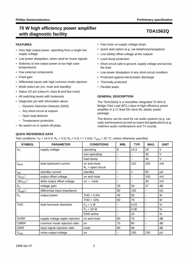
FEATURES
• Very high output power, operating from a single lowsupply voltage
• Low power dissipation, when used for music signals
• Switches to low output power at too high casetemperatures
• Few external components
• Fixed gain
• Differential inputs with high common mode rejection
• Mode select pin (on, mute and standby)
• Status I/O pin (class-H, class-B and fast mute)
• All switching levels with hysteresis
• Diagnostic pin with information about:
– Dynamic Distortion Detector (DDD)
– Any short-circuit at outputs
– Open load detector
– Temperature protection.
• No switch-on or switch-off plops
• Fast mute on supply voltage drops
• Quick start option (e.g. car-telephony/navigation)
• Low (delta) offset voltage at the outputs
• Load dump protection
• Short-circuit safe to ground, supply voltage and acrossthe load
• Low power dissipation in any short-circuit condition
• Protected against electrostatic discharge
• Thermally protected
• Flexible leads.
GENERAL DESCRIPTION
The TDA1562Q is a monolithic integrated 70 W/4 ΩBridge-Tied Load (BTL) class-H high efficiency poweramplifier in a 17-lead DIL-bent-SIL plastic powerpackage.
The device can be used for car audio systems (e.g. car,radio and boosters) as well as mains fed applications (e.g.midi/mini audio combinations and TV sound).
QUICK REFERENCE DATATest conditions: VP = 14.4 V; RL = 4 Ω; Rs = 0 Ω; f = 1 kHz; Tamb = 25 °C; unless otherwise specified.
SYMBOL PARAMETER CONDITIONS MIN. TYP. MAX. UNIT
VP supply voltage operating 8 14.4 18 V
non-operating − − 30 V
load dump − − 45 V
Iq(tot) total quiescent current on and mute;RL = open circuit
− 110 150 mA
Istb standby current standby − 1 50 µA
VOO output offset voltage on and mute − − 100 mV
∆VOO delta output offset voltage on ↔ mute − − 30 mV
Gv voltage gain 25 26 27 dB
Zi(dif) differential input impedance 90 150 − kΩPo output power THD = 0.5% 45 55 − W
THD = 10% 60 70 − W
THD total harmonic distortion Po = 1 W − 0.03 − %
Po = 20 W − 0.06 − %
DDD active − 10 − %
SVRR supply voltage ripple rejection on and mute 60 70 − dB
CMRR common mode rejection ratio on 70 80 − dB
ISRR input signal rejection ratio mute 80 90 − dB
Vn(o) noise output voltage on − 100 150 µV
1998 Apr 07 3
Philips Semiconductors Preliminary specification
70 W high efficiency power amplifierwith diagnostic facility
TDA1562Q
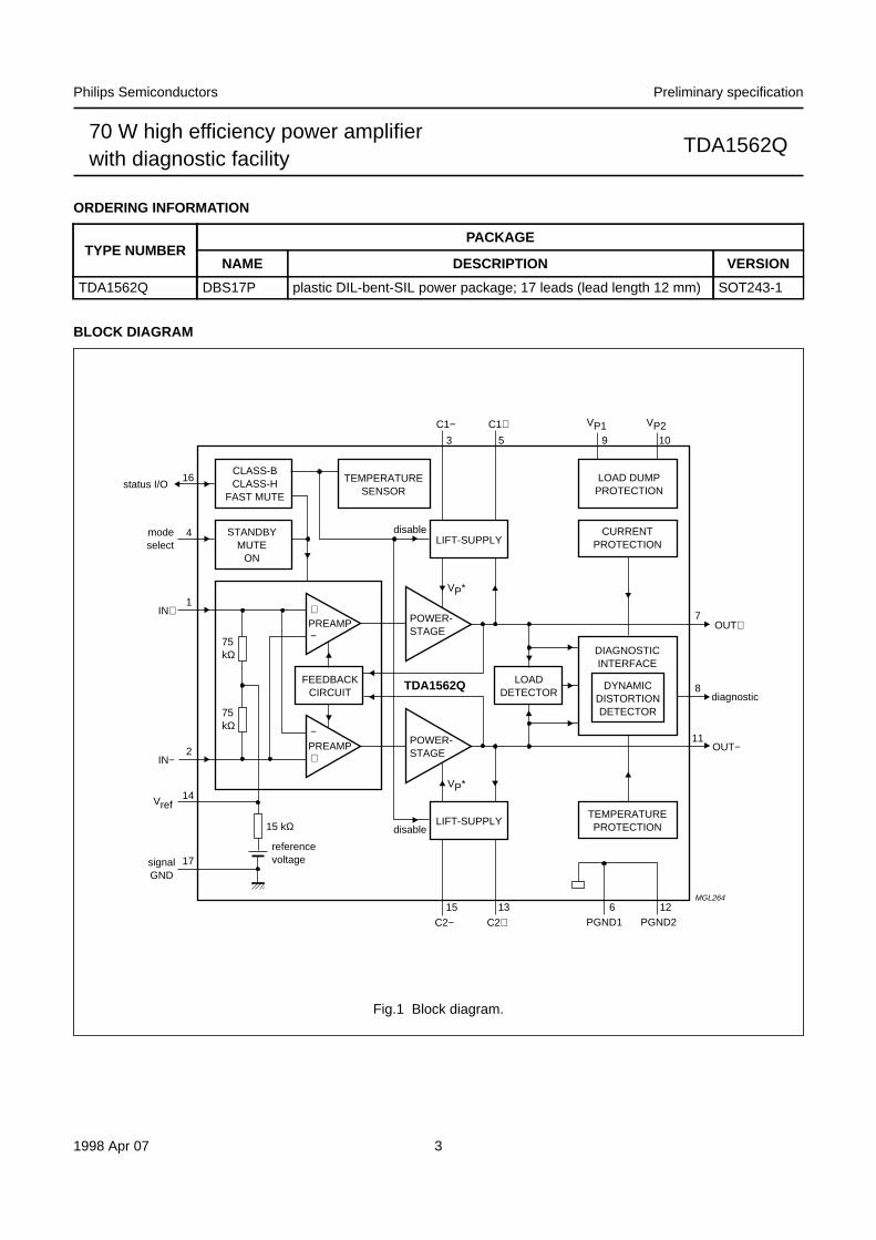
ORDERING INFORMATION
BLOCK DIAGRAM
TYPE NUMBERPACKAGE
NAME DESCRIPTION VERSION
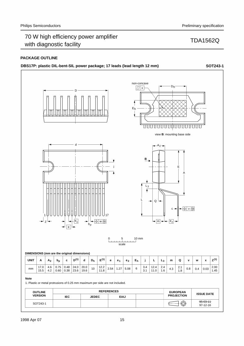
TDA1562Q DBS17P plastic DIL-bent-SIL power package; 17 leads (lead length 12 mm) SOT243-1
Fig.1 Block diagram.
handbook, full pagewidth
POWER-STAGE
PREAMP
status I/O
VP*
VP*
75kΩ
−
+
C1+C1−
FEEDBACKCIRCUIT
TDA1562Q
POWER-STAGE
CLASS-BCLASS-H
FAST MUTE
TEMPERATURESENSOR
LOAD DUMPPROTECTION
STANDBYMUTE
ON
LOADDETECTOR
DYNAMICDISTORTIONDETECTOR
DIAGNOSTICINTERFACE
TEMPERATUREPROTECTION
CURRENTPROTECTIONLIFT-SUPPLY
LIFT-SUPPLYdisable
disable
16
modeselect
4
1IN+
3 5
75kΩ
15 kΩ
referencevoltage
PREAMP−
+2
IN−
14Vref
17signalGND
C2+C2−
OUT−
15 13 6PGND1 PGND2
MGL26412
11
diagnostic
OUT+7
8
9 10
VP2VP1
1998 Apr 07 4
Philips Semiconductors Preliminary specification
70 W high efficiency power amplifierwith diagnostic facility
TDA1562Q
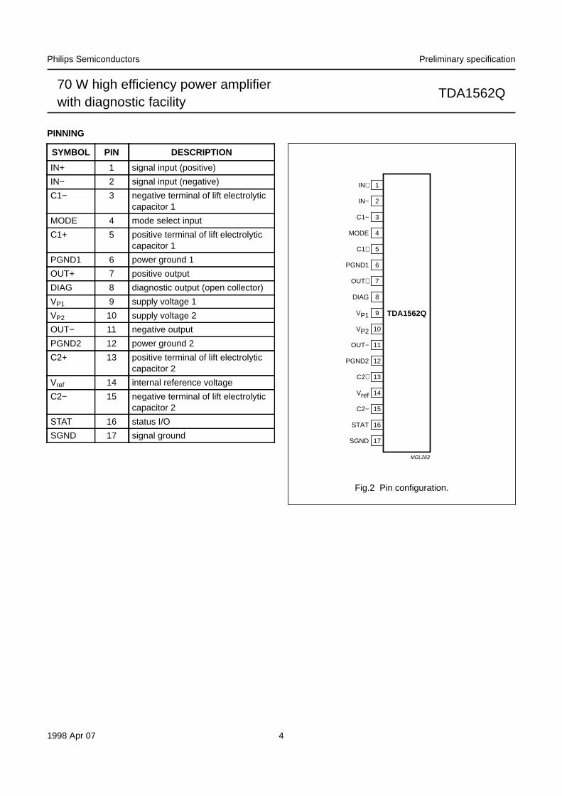
PINNING
SYMBOL PIN DESCRIPTION
IN+ 1 signal input (positive)
IN− 2 signal input (negative)
C1− 3 negative terminal of lift electrolyticcapacitor 1
MODE 4 mode select input
C1+ 5 positive terminal of lift electrolyticcapacitor 1
PGND1 6 power ground 1
OUT+ 7 positive output
DIAG 8 diagnostic output (open collector)
VP1 9 supply voltage 1
VP2 10 supply voltage 2
OUT− 11 negative output
PGND2 12 power ground 2
C2+ 13 positive terminal of lift electrolyticcapacitor 2
Vref 14 internal reference voltage
C2− 15 negative terminal of lift electrolyticcapacitor 2
STAT 16 status I/O
SGND 17 signal ground
Fig.2 Pin configuration.
handbook, halfpage
TDA1562Q
MGL263
1
2
3
4
5
6
7
8
9
10
11
12
13
14
15
16
17
IN+
IN−
C1−
MODE
C1+
PGND1
OUT+
DIAG
VP1
VP2
OUT−
PGND2
C2+
Vref
C2−
STAT
SGND
1998 Apr 07 5
Philips Semiconductors Preliminary specification
70 W high efficiency power amplifierwith diagnostic facility
TDA1562Q
FUNCTIONAL DESCRIPTION
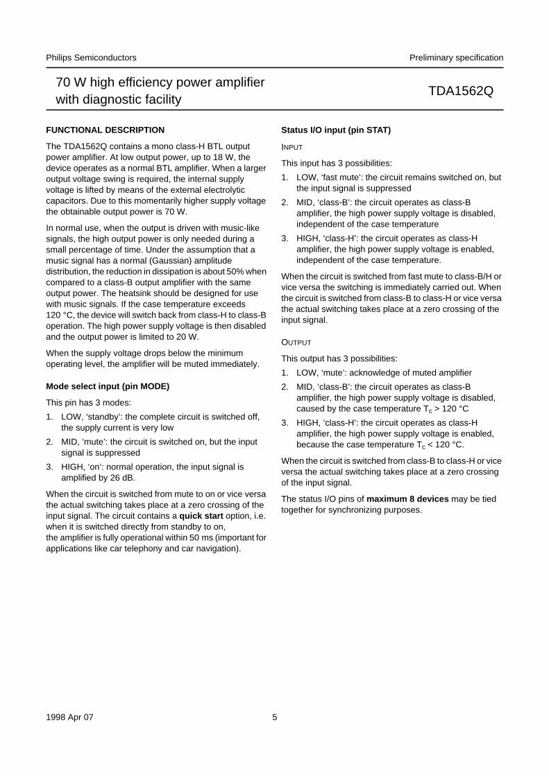
The TDA1562Q contains a mono class-H BTL outputpower amplifier. At low output power, up to 18 W, thedevice operates as a normal BTL amplifier. When a largeroutput voltage swing is required, the internal supplyvoltage is lifted by means of the external electrolyticcapacitors. Due to this momentarily higher supply voltagethe obtainable output power is 70 W.
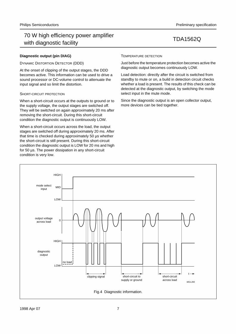
In normal use, when the output is driven with music-likesignals, the high output power is only needed during asmall percentage of time. Under the assumption that amusic signal has a normal (Gaussian) amplitudedistribution, the reduction in dissipation is about 50% whencompared to a class-B output amplifier with the sameoutput power. The heatsink should be designed for usewith music signals. If the case temperature exceeds120 °C, the device will switch back from class-H to class-Boperation. The high power supply voltage is then disabledand the output power is limited to 20 W.
When the supply voltage drops below the minimumoperating level, the amplifier will be muted immediately.
Mode select input (pin MODE)
This pin has 3 modes:
1. LOW, ‘standby’: the complete circuit is switched off,the supply current is very low
2. MID, ‘mute’: the circuit is switched on, but the inputsignal is suppressed
3. HIGH, ‘on’: normal operation, the input signal isamplified by 26 dB.
When the circuit is switched from mute to on or vice versathe actual switching takes place at a zero crossing of theinput signal. The circuit contains a quick start option, i.e.when it is switched directly from standby to on,the amplifier is fully operational within 50 ms (important forapplications like car telephony and car navigation).
Status I/O input (pin STAT)
INPUT
This input has 3 possibilities:
1. LOW, ‘fast mute’: the circuit remains switched on, butthe input signal is suppressed
2. MID, ‘class-B’: the circuit operates as class-Bamplifier, the high power supply voltage is disabled,independent of the case temperature
3. HIGH, ‘class-H’: the circuit operates as class-Hamplifier, the high power supply voltage is enabled,independent of the case temperature.
When the circuit is switched from fast mute to class-B/H orvice versa the switching is immediately carried out. Whenthe circuit is switched from class-B to class-H or vice versathe actual switching takes place at a zero crossing of theinput signal.
OUTPUT
This output has 3 possibilities:
1. LOW, ‘mute’: acknowledge of muted amplifier
2. MID, ‘class-B’: the circuit operates as class-Bamplifier, the high power supply voltage is disabled,caused by the case temperature Tc > 120 °C
3. HIGH, ‘class-H’: the circuit operates as class-Hamplifier, the high power supply voltage is enabled,because the case temperature Tc < 120 °C.
When the circuit is switched from class-B to class-H or viceversa the actual switching takes place at a zero crossingof the input signal.
The status I/O pins of maximum 8 devices may be tiedtogether for synchronizing purposes.
1998 Apr 07 6
Philips Semiconductors Preliminary specification
70 W high efficiency power amplifierwith diagnostic facility
TDA1562Q
Fig.3 Switching characteristics.
handbook, full pagewidthon
mute
0
supplyvoltage
referencevoltage
mode selectinput
status I/Oinput
HIGH
MID
LOW
HIGH
MID
class-H (Tc < 120 °C)
class-B (Tc > 120 °C)
LOW
status I/Ooutput
HIGH
MID
LOW
Vref
VRT
0
output voltageacross load 0
zerocross changeclass B/H-operation
zerocross mutefunction
fast mutefunction
quick startmute
supply mutefunction
MGL272
1998 Apr 07 7
Philips Semiconductors Preliminary specification
70 W high efficiency power amplifierwith diagnostic facility
TDA1562Q
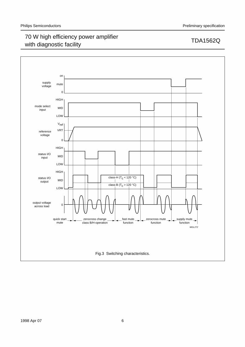
Diagnostic output (pin DIAG)
DYNAMIC DISTORTION DETECTOR (DDD)
At the onset of clipping of the output stages, the DDDbecomes active. This information can be used to drive asound processor or DC-volume control to attenuate theinput signal and so limit the distortion.
SHORT-CIRCUIT PROTECTION
When a short-circuit occurs at the outputs to ground or tothe supply voltage, the output stages are switched off.They will be switched on again approximately 20 ms afterremoving the short-circuit. During this short-circuitcondition the diagnostic output is continuously LOW.
When a short-circuit occurs across the load, the outputstages are switched off during approximately 20 ms. Afterthat time is checked during approximately 50 µs whetherthe short-circuit is still present. During this short-circuitcondition the diagnostic output is LOW for 20 ms and highfor 50 µs. The power dissipation in any short-circuitcondition is very low.
TEMPERATURE DETECTION
Just before the temperature protection becomes active thediagnostic output becomes continuously LOW.
Load detection: directly after the circuit is switched fromstandby to mute or on, a build in detection circuit checkswhether a load is present. The results of this check can bedetected at the diagnostic output, by switching the modeselect input in the mute mode.
Since the diagnostic output is an open collector output,more devices can be tied together.
Fig.4 Diagnostic information.
handbook, full pagewidth
HIGH
MID
LOW
mode selectinput
diagnosticoutput
output voltageacross load 0
HIGH
LOWno load
clipping signal short-circuit tosupply or ground
short-circuitacross load
t
MGL265
1998 Apr 07 8
Philips Semiconductors Preliminary specification
70 W high efficiency power amplifierwith diagnostic facility
TDA1562Q
LIMITING VALUESIn accordance with the Absolute Maximum Rating System (IEC 134).
Note
1. Tj is a theoretical temperature which is based on a simplified representation of the thermal behaviour of the device.Tj = Tc + P × Rth(j-c), where Rth(j-c) is a fixed value to be used for the calculation of Tj. The rating for Tj limits theallowable combinations of power dissipation P and case temperature Tc (in accordance with IEC 747-1).
SYMBOL PARAMETER CONDITIONS MIN. MAX. UNIT
VP supply voltage operating − 18 V
non-operating − 30 V
load dump; tr > 2.5 ms;T = 50 ms
− 45 V
IOSM non-repetitive peak output current − 10 A
repetitive peak output current − 8 A
Vsc short-circuit safe voltage − 18 V
Tstg storage temperature −55 +150 °CTamb ambient temperature −40 − °CTj junction temperature note 1 − 150 °CPtot total power dissipation − 60 W
Fig.5 Behaviour as a function of temperature.
handbook, full pagewidthclass-H
maximum outputvoltage swing
diagnosticoutput
status I/O: high
status I/O: open
MGL266
class-B
0
HIGH
LOW
status I/Ooutput
HIGH
MID
LOW120 145
Tj (°C)150 160100
1998 Apr 07 9
Philips Semiconductors Preliminary specification
70 W high efficiency power amplifierwith diagnostic facility
TDA1562Q
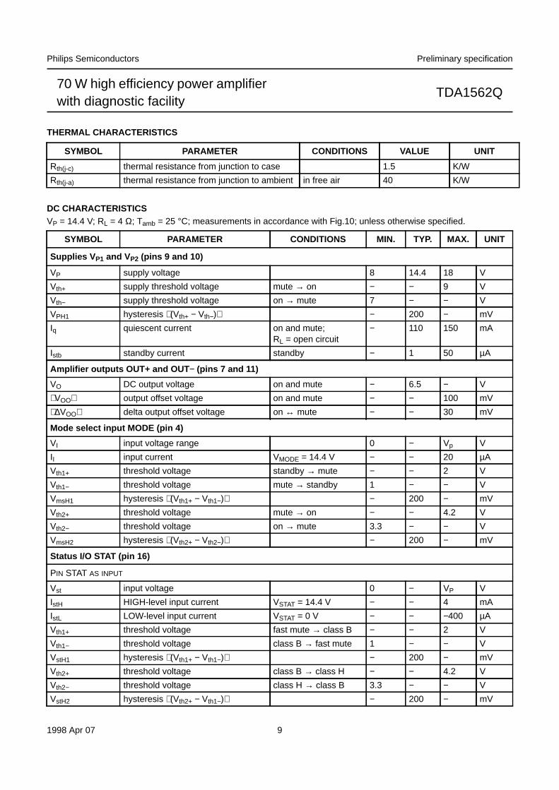
THERMAL CHARACTERISTICS
DC CHARACTERISTICSVP = 14.4 V; RL = 4 Ω; Tamb = 25 °C; measurements in accordance with Fig.10; unless otherwise specified.
SYMBOL PARAMETER CONDITIONS VALUE UNIT
Rth(j-c) thermal resistance from junction to case 1.5 K/W
Rth(j-a) thermal resistance from junction to ambient in free air 40 K/W
SYMBOL PARAMETER CONDITIONS MIN. TYP. MAX. UNIT
Supplies V P1 and VP2 (pins 9 and 10)
VP supply voltage 8 14.4 18 V
Vth+ supply threshold voltage mute → on − − 9 V
Vth− supply threshold voltage on → mute 7 − − V
VPH1 hysteresis (Vth+ − Vth−) − 200 − mV
Iq quiescent current on and mute;RL = open circuit
− 110 150 mA
Istb standby current standby − 1 50 µA
Amplifier outputs OUT+ and OUT − (pins 7 and 11)
VO DC output voltage on and mute − 6.5 − V
VOO output offset voltage on and mute − − 100 mV
∆VOO delta output offset voltage on ↔ mute − − 30 mV
Mode select input MODE (pin 4)
VI input voltage range 0 − Vp V
II input current VMODE = 14.4 V − − 20 µA
Vth1+ threshold voltage standby → mute − − 2 V
Vth1− threshold voltage mute → standby 1 − − V
VmsH1 hysteresis (Vth1+ − Vth1−) − 200 − mV
Vth2+ threshold voltage mute → on − − 4.2 V
Vth2− threshold voltage on → mute 3.3 − − V
VmsH2 hysteresis (Vth2+ − Vth2−) − 200 − mV
Status I/O STAT (pin 16)
PIN STAT AS INPUT
Vst input voltage 0 − VP V
IstH HIGH-level input current VSTAT = 14.4 V − − 4 mA
IstL LOW-level input current VSTAT = 0 V − − −400 µA
Vth1+ threshold voltage fast mute → class B − − 2 V
Vth1− threshold voltage class B → fast mute 1 − − V
VstH1 hysteresis (Vth1+ − Vth1−) − 200 − mV
Vth2+ threshold voltage class B → class H − − 4.2 V
Vth2− threshold voltage class H → class B 3.3 − − V
VstH2 hysteresis (Vth2+ − Vth1−) − 200 − mV
1998 Apr 07 10
Philips Semiconductors Preliminary specification
70 W high efficiency power amplifierwith diagnostic facility
TDA1562Q
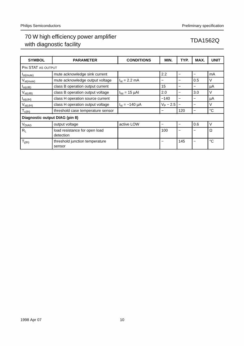
PIN STAT AS OUTPUT
Ist(mute) mute acknowledge sink current 2.2 − − mA
Vst(mute) mute acknowledge output voltage Ist = 2.2 mA − − 0.5 V
Ist(clB) class B operation output current 15 − − µA
Vst(clB) class B operation output voltage IIst = 15 µAI 2.0 − 3.0 V
Ist(clH) class H operation source current −140 − − µA
Vst(clH) class H operation output voltage Ist = −140 µA VP − 2.5 − − V
Tc(th) threshold case temperature sensor − 120 − °C
Diagnostic output DIAG (pin 8)
VDIAG output voltage active LOW − − 0.6 V
RL load resistance for open loaddetection
100 − − Ω
Tj(th) threshold junction temperaturesensor
− 145 − °C
SYMBOL PARAMETER CONDITIONS MIN. TYP. MAX. UNIT

1998 Apr 07 11
Philips Semiconductors Preliminary specification
70 W high efficiency power amplifierwith diagnostic facility
TDA1562Q
Fig.6 Supply voltage transfer characteristic.
handbook, full pagewidth
VPH1
Vth− Vth+ MGL267
fast mute
on-mode
VP
Fig.7 Mode select transfer characteristic.
handbook, full pagewidth
VmsH1 VmsH2 Vms
Vth1− Vth1+ Vth2− Vth2+MGL268
standby
mute
on-mode
Fig.8 Status I/O transfer characteristic.
handbook, full pagewidth
VstH1 VstH2
Vth1− Vth1+ Vth2− Vth2+MGL269
fast mute
class-B
class-H
Vst
1998 Apr 07 12
Philips Semiconductors Preliminary specification
70 W high efficiency power amplifierwith diagnostic facility
TDA1562Q
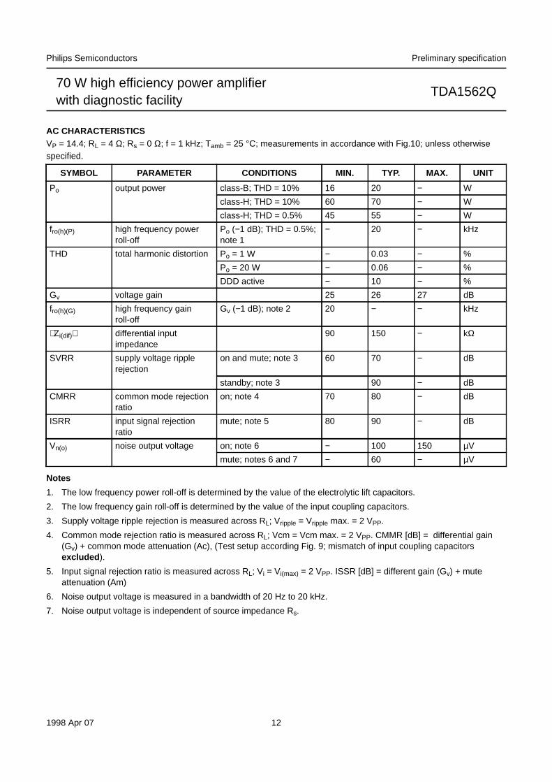
AC CHARACTERISTICSVP = 14.4; RL = 4 Ω; Rs = 0 Ω; f = 1 kHz; Tamb = 25 °C; measurements in accordance with Fig.10; unless otherwisespecified.
Notes
1. The low frequency power roll-off is determined by the value of the electrolytic lift capacitors.
2. The low frequency gain roll-off is determined by the value of the input coupling capacitors.
3. Supply voltage ripple rejection is measured across RL; Vripple = Vripple max. = 2 VPP.
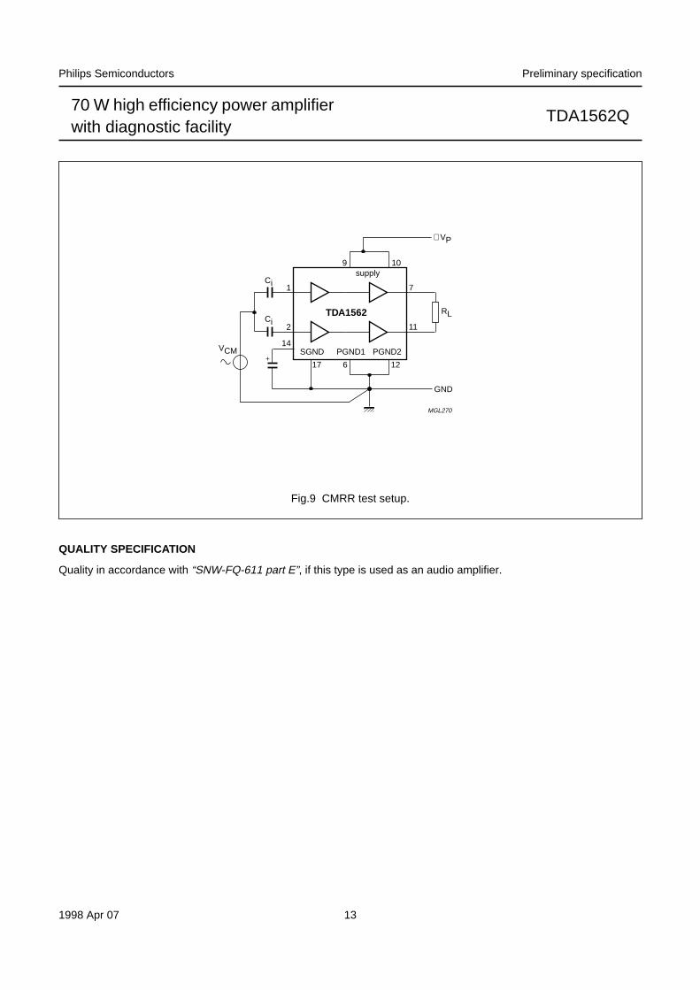
4. Common mode rejection ratio is measured across RL; Vcm = Vcm max. = 2 VPP. CMMR [dB] = differential gain(Gv) + common mode attenuation (Ac), (Test setup according Fig. 9; mismatch of input coupling capacitorsexcluded ).
5. Input signal rejection ratio is measured across RL; Vi = Vi(max) = 2 VPP. ISSR [dB] = different gain (Gv) + muteattenuation (Am)
6. Noise output voltage is measured in a bandwidth of 20 Hz to 20 kHz.
7. Noise output voltage is independent of source impedance Rs.
SYMBOL PARAMETER CONDITIONS MIN. TYP. MAX. UNIT
Po output power class-B; THD = 10% 16 20 − W
class-H; THD = 10% 60 70 − W
class-H; THD = 0.5% 45 55 − W
fro(h)(P) high frequency powerroll-off
Po (−1 dB); THD = 0.5%;note 1
− 20 − kHz
THD total harmonic distortion Po = 1 W − 0.03 − %
Po = 20 W − 0.06 − %
DDD active − 10 − %
Gv voltage gain 25 26 27 dB
fro(h)(G) high frequency gainroll-off
Gv (−1 dB); note 2 20 − − kHz
Zi(dif) differential inputimpedance
90 150 − kΩ
SVRR supply voltage ripplerejection
on and mute; note 3 60 70 − dB
standby; note 3 90 − dB
CMRR common mode rejectionratio
on; note 4 70 80 − dB
ISRR input signal rejectionratio
mute; note 5 80 90 − dB
Vn(o) noise output voltage on; note 6 − 100 150 µV
mute; notes 6 and 7 − 60 − µV
1998 Apr 07 13
Philips Semiconductors Preliminary specification
70 W high efficiency power amplifierwith diagnostic facility
TDA1562Q
QUALITY SPECIFICATION
Quality in accordance with “SNW-FQ-611 part E”, if this type is used as an audio amplifier.
Fig.9 CMRR test setup.
handbook, full pagewidth
TDA1562
supply10
MGL270
7
11
1217
14
2
1
6
+ VP
RL
VCM
Ci
Ci
GND
9
SGND PGND1 PGND2
1998A
pr07
14
Philips S
emiconductors
Prelim
inary specification
70 W high efficiency pow
er amplifier
with diagnostic facility
TD
A1562Q
This text is here in white to force landscape pages to be rotated correctly when browsing through the pdf in the Acrobat reader.This text is here in_white to force landscape pages to be rotated correctly when browsing through the pdf in the Acrobat reader.This text is here inThis text is here inwhite to force landscape pages to be rotated correctly when browsing through the pdf in the Acrobat reader. white to force landscape pages to be ...
TE
ST
AN
D A
PP
LICAT
ION
INF
OR
MAT
ION
hand
book
, ful
l pag
ewid
th
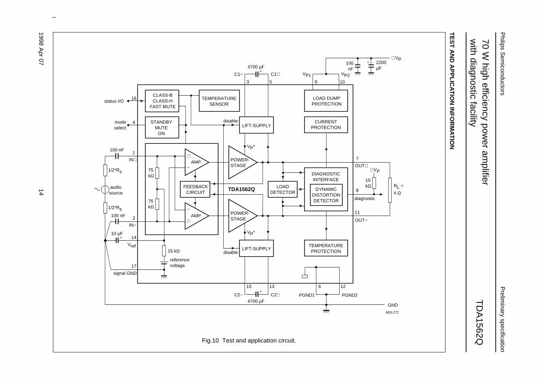
POWER-STAGE
AMP.
status I/O
VP*
VP*
75kΩ
10kΩ RL =
4 Ω
−
+
C1+C1−
FEEDBACKCIRCUIT
TDA1562Q
POWER-STAGE
CLASS-BCLASS-H
FAST MUTE
TEMPERATURESENSOR
LOAD DUMPPROTECTION
STANDBYMUTE
ON
LOADDETECTOR
DYNAMICDISTORTIONDETECTOR
DIAGNOSTICINTERFACE
TEMPERATUREPROTECTION
CURRENTPROTECTIONLIFT-SUPPLY
LIFT-SUPPLYdisable
disable
16
modeselect
4
1
IN+
100 nF
3 5
4700 µF2200µF
100nF
75kΩ
15 kΩ
referencevoltage
AMP.−
+2
audiosource
1/2*Rs
1/2*Rs
IN−
14
Vref
17
signal GND
100 nF
10 µF
C2+C2−
OUT−
15 13 6
GND
MGL271
12
11
diagnostic
OUT++ VP
7
8
4700 µF
9 10
+ VP
VP2VP1
PGND1 PGND2
Fig.10 Test and application circuit.
1998 Apr 07 15
Philips Semiconductors Preliminary specification
70 W high efficiency power amplifierwith diagnostic facility
TDA1562Q
PACKAGE OUTLINE
REFERENCESOUTLINEVERSION
EUROPEANPROJECTION ISSUE DATE
IEC JEDEC EIAJ
DIMENSIONS (mm are the original dimensions)
Note
1. Plastic or metal protrusions of 0.25 mm maximum per side are not included.
SOT243-1
0 5 10 mm
scale
D
L
E
A
c
A2
L3
Q
w Mbp
1
d
D
Z e
e
x h
1 17
j
Eh
non-concave
95-03-1197-12-16
DBS17P: plastic DIL-bent-SIL power package; 17 leads (lead length 12 mm) SOT243-1
view B: mounting base side
m 2e
v M
B
UNIT A e 1A2 bp c D(1) E(1) Z(1)d eDh L L3 m
mm 17.015.5
4.64.2
0.750.60
0.480.38
24.023.6
20.019.6
10 2.54
v
0.812.211.8
1.27
e 2
5.08 2.41.6
Eh
6 2.001.45
2.11.8
3.43.1 4.3
12.411.0
Qj
0.4
w
0.03
x
1998 Apr 07 16
Philips Semiconductors Preliminary specification
70 W high efficiency power amplifierwith diagnostic facility
TDA1562Q
SOLDERING
Introduction
There is no soldering method that is ideal for all ICpackages. Wave soldering is often preferred whenthrough-hole and surface mounted components are mixedon one printed-circuit board. However, wave soldering isnot always suitable for surface mounted ICs, or forprinted-circuits with high population densities. In thesesituations reflow soldering is often used.
This text gives a very brief insight to a complex technology.A more in-depth account of soldering ICs can be found inour “IC Package Databook” (order code 9398 652 90011).
Soldering by dipping or by wave
The maximum permissible temperature of the solder is260 °C; solder at this temperature must not be in contactwith the joint for more than 5 seconds. The total contacttime of successive solder waves must not exceed5 seconds.
The device may be mounted up to the seating plane, butthe temperature of the plastic body must not exceed thespecified maximum storage temperature (Tstg max). If theprinted-circuit board has been pre-heated, forced coolingmay be necessary immediately after soldering to keep thetemperature within the permissible limit.
Repairing soldered joints
Apply a low voltage soldering iron (less than 24 V) to thelead(s) of the package, below the seating plane or notmore than 2 mm above it. If the temperature of thesoldering iron bit is less than 300 °C it may remain incontact for up to 10 seconds. If the bit temperature isbetween 300 and 400 °C, contact may be up to 5 seconds.
DEFINITIONS
LIFE SUPPORT APPLICATIONS
These products are not designed for use in life support appliances, devices, or systems where malfunction of theseproducts can reasonably be expected to result in personal injury. Philips customers using or selling these products foruse in such applications do so at their own risk and agree to fully indemnify Philips for any damages resulting from suchimproper use or sale.
Data sheet status
Objective specification This data sheet contains target or goal specifications for product development.
Preliminary specification This data sheet contains preliminary data; supplementary data may be published later.
Product specification This data sheet contains final product specifications.
Limiting values
Limiting values given are in accordance with the Absolute Maximum Rating System (IEC 134). Stress above one ormore of the limiting values may cause permanent damage to the device. These are stress ratings only and operationof the device at these or at any other conditions above those given in the Characteristics sections of the specificationis not implied. Exposure to limiting values for extended periods may affect device reliability.
Application information
Where application information is given, it is advisory and does not form part of the specification.

1998 Apr 07 17
Philips Semiconductors Preliminary specification
70 W high efficiency power amplifierwith diagnostic facility
TDA1562Q
NOTES

1998 Apr 07 18
Philips Semiconductors Preliminary specification
70 W high efficiency power amplifierwith diagnostic facility
TDA1562Q
NOTES

1998 Apr 07 19
Philips Semiconductors Preliminary specification
70 W high efficiency power amplifierwith diagnostic facility
TDA1562Q
NOTES

Internet: http://www.semiconductors.philips.com
Philips Semiconductors – a worldwide company
© Philips Electronics N.V. 1998 SCA59
All rights are reserved. Reproduction in whole or in part is prohibited without the prior written consent of the copyright owner.
The information presented in this document does not form part of any quotation or contract, is believed to be accurate and reliable and may be changedwithout notice. No liability will be accepted by the publisher for any consequence of its use. Publication thereof does not convey nor imply any licenseunder patent- or other industrial or intellectual property rights.
Middle East: see Italy
Netherlands: Postbus 90050, 5600 PB EINDHOVEN, Bldg. VB,Tel. +31 40 27 82785, Fax. +31 40 27 88399
New Zealand: 2 Wagener Place, C.P.O. Box 1041, AUCKLAND,Tel. +64 9 849 4160, Fax. +64 9 849 7811
Norway: Box 1, Manglerud 0612, OSLO,Tel. +47 22 74 8000, Fax. +47 22 74 8341
Pakistan: see Singapore
Philippines: Philips Semiconductors Philippines Inc.,106 Valero St. Salcedo Village, P.O. Box 2108 MCC, MAKATI,Metro MANILA, Tel. +63 2 816 6380, Fax. +63 2 817 3474
Poland: Ul. Lukiska 10, PL 04-123 WARSZAWA,Tel. +48 22 612 2831, Fax. +48 22 612 2327
Portugal: see Spain
Romania: see Italy
Russia: Philips Russia, Ul. Usatcheva 35A, 119048 MOSCOW,Tel. +7 095 755 6918, Fax. +7 095 755 6919
Singapore: Lorong 1, Toa Payoh, SINGAPORE 319762,Tel. +65 350 2538, Fax. +65 251 6500
Slovakia: see Austria
Slovenia: see Italy
South Africa: S.A. PHILIPS Pty Ltd., 195-215 Main Road Martindale,2092 JOHANNESBURG, P.O. Box 7430 Johannesburg 2000,Tel. +27 11 470 5911, Fax. +27 11 470 5494
South America: Al. Vicente Pinzon, 173, 6th floor,04547-130 SÃO PAULO, SP, Brazil,Tel. +55 11 821 2333, Fax. +55 11 821 2382
Spain: Balmes 22, 08007 BARCELONA,Tel. +34 3 301 6312, Fax. +34 3 301 4107
Sweden: Kottbygatan 7, Akalla, S-16485 STOCKHOLM,Tel. +46 8 5985 2000, Fax. +46 8 5985 2745
Switzerland: Allmendstrasse 140, CH-8027 ZÜRICH,Tel. +41 1 488 2741 Fax. +41 1 488 3263
Taiwan: Philips Semiconductors, 6F, No. 96, Chien Kuo N. Rd., Sec. 1,TAIPEI, Taiwan Tel. +886 2 2134 2865, Fax. +886 2 2134 2874
Thailand: PHILIPS ELECTRONICS (THAILAND) Ltd.,209/2 Sanpavuth-Bangna Road Prakanong, BANGKOK 10260,Tel. +66 2 745 4090, Fax. +66 2 398 0793
Turkey: Talatpasa Cad. No. 5, 80640 GÜLTEPE/ISTANBUL,Tel. +90 212 279 2770, Fax. +90 212 282 6707
Ukraine : PHILIPS UKRAINE, 4 Patrice Lumumba str., Building B, Floor 7,252042 KIEV, Tel. +380 44 264 2776, Fax. +380 44 268 0461
United Kingdom: Philips Semiconductors Ltd., 276 Bath Road, Hayes,MIDDLESEX UB3 5BX, Tel. +44 181 730 5000, Fax. +44 181 754 8421
United States: 811 East Arques Avenue, SUNNYVALE, CA 94088-3409,Tel. +1 800 234 7381
Uruguay: see South America
Vietnam: see Singapore
Yugoslavia: PHILIPS, Trg N. Pasica 5/v, 11000 BEOGRAD,Tel. +381 11 625 344, Fax.+381 11 635 777
For all other countries apply to: Philips Semiconductors,International Marketing & Sales Communications, Building BE-p, P.O. Box 218,5600 MD EINDHOVEN, The Netherlands, Fax. +31 40 27 24825
Argentina: see South America
Australia: 34 Waterloo Road, NORTH RYDE, NSW 2113,Tel. +61 2 9805 4455, Fax. +61 2 9805 4466
Austria: Computerstr. 6, A-1101 WIEN, P.O. Box 213, Tel. +43 160 1010,Fax. +43 160 101 1210
Belarus: Hotel Minsk Business Center, Bld. 3, r. 1211, Volodarski Str. 6,220050 MINSK, Tel. +375 172 200 733, Fax. +375 172 200 773
Belgium: see The Netherlands
Brazil: see South America
Bulgaria: Philips Bulgaria Ltd., Energoproject, 15th floor,51 James Bourchier Blvd., 1407 SOFIA,Tel. +359 2 689 211, Fax. +359 2 689 102
Canada: PHILIPS SEMICONDUCTORS/COMPONENTS,Tel. +1 800 234 7381
China/Hong Kong: 501 Hong Kong Industrial Technology Centre,72 Tat Chee Avenue, Kowloon Tong, HONG KONG,Tel. +852 2319 7888, Fax. +852 2319 7700
Colombia: see South America
Czech Republic: see Austria
Denmark: Prags Boulevard 80, PB 1919, DK-2300 COPENHAGEN S,Tel. +45 32 88 2636, Fax. +45 31 57 0044
Finland: Sinikalliontie 3, FIN-02630 ESPOO,Tel. +358 9 615800, Fax. +358 9 61580920
France: 51 Rue Carnot, BP317, 92156 SURESNES Cedex,Tel. +33 1 40 99 6161, Fax. +33 1 40 99 6427
Germany: Hammerbrookstraße 69, D-20097 HAMBURG,Tel. +49 40 23 53 60, Fax. +49 40 23 536 300
Greece: No. 15, 25th March Street, GR 17778 TAVROS/ATHENS,Tel. +30 1 4894 339/239, Fax. +30 1 4814 240
Hungary: see Austria
India: Philips INDIA Ltd, Band Box Building, 2nd floor,254-D, Dr. Annie Besant Road, Worli, MUMBAI 400 025,Tel. +91 22 493 8541, Fax. +91 22 493 0966
Indonesia: PT Philips Development Corporation, Semiconductors Division,Gedung Philips, Jl. Buncit Raya Kav.99-100, JAKARTA 12510,Tel. +62 21 794 0040 ext. 2501, Fax. +62 21 794 0080
Ireland: Newstead, Clonskeagh, DUBLIN 14,Tel. +353 1 7640 000, Fax. +353 1 7640 200
Israel: RAPAC Electronics, 7 Kehilat Saloniki St, PO Box 18053,TEL AVIV 61180, Tel. +972 3 645 0444, Fax. +972 3 649 1007
Italy: PHILIPS SEMICONDUCTORS, Piazza IV Novembre 3,20124 MILANO, Tel. +39 2 6752 2531, Fax. +39 2 6752 2557
Japan: Philips Bldg 13-37, Kohnan 2-chome, Minato-ku, TOKYO 108,Tel. +81 3 3740 5130, Fax. +81 3 3740 5077
Korea: Philips House, 260-199 Itaewon-dong, Yongsan-ku, SEOUL,Tel. +82 2 709 1412, Fax. +82 2 709 1415
Malaysia: No. 76 Jalan Universiti, 46200 PETALING JAYA, SELANGOR,Tel. +60 3 750 5214, Fax. +60 3 757 4880
Mexico: 5900 Gateway East, Suite 200, EL PASO, TEXAS 79905,Tel. +9-5 800 234 7381
Printed in The Netherlands 545102/1200/01/pp20 Date of release: 1998 Apr 07 Document order number: 9397 750 03043

WWW.ALLDATASHEET.COM
Copyright © Each Manufacturing Company.
All Datasheets cannot be modified without permission.
This datasheet has been download from :
www.AllDataSheet.com
100% Free DataSheet Search Site.
Free Download.
No Register.
Fast Search System.
www.AllDataSheet.com


