Embed Size (px)
DESCRIPTION
The operational Amplifier (Part 2) Floyd 7 ed
Citation preview

Engr.Tehseen Ahsan
Lecturer, Electrical Engineering Department
EE-307 Electronic Systems Design
HITEC University Taxila Cantt, Pakistan
The Operational Amplifier (Part 2)

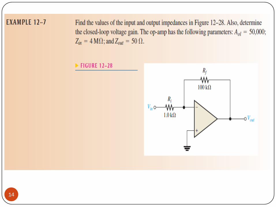
12-5 Effect of Negative FeedBack On OP-AMP Impedances
Impedances of a Non-inverting Amplifier
Input Impedance
The input impedance of a non-inverting amplifier can be developed with
the aid of figure 12-23.
For this Analysis, assume a small differential voltage, Vd, exists between
the two input terminals as indicated. This means that you cannot assume
the op-amp’s input impedance to be infinite or the input current to be 0.
2

12-5 Effect of Negative FeedBack On OP-AMP Impedances Continue…
Impedances of a Non-inverting Amplifier
Input Impedance continue…
The input voltage can be expressed as
3

12-5 Effect of Negative FeedBack On OP-AMP Impedances Continue…
Impedances of a Non-inverting Amplifier
Input Impedance continue…
4

12-5 Effect of Negative FeedBack On OP-AMP Impedances Continue…
Impedances of a Non-inverting Amplifier
Output Impedance
An expression for output impedance of a non-inverting amplifier can be
developed with the aid of figure 12-24.
5

12-5 Effect of Negative FeedBack On OP-AMP Impedances Continue…
Impedances of a Non-inverting Amplifier
Output Impedance continue…
By applying KVL to the output circuit of fig 12-24
6

12-5 Effect of Negative FeedBack On OP-AMP Impedances Continue…
Impedances of a Non-inverting Amplifier
Output Impedance continue…
7

8
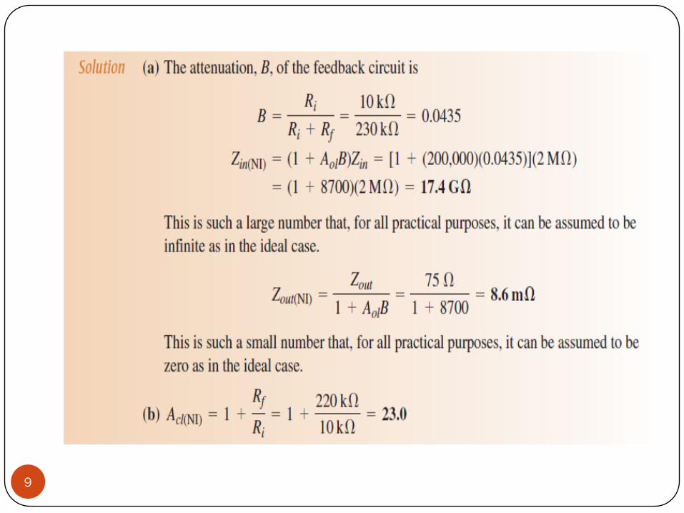
9

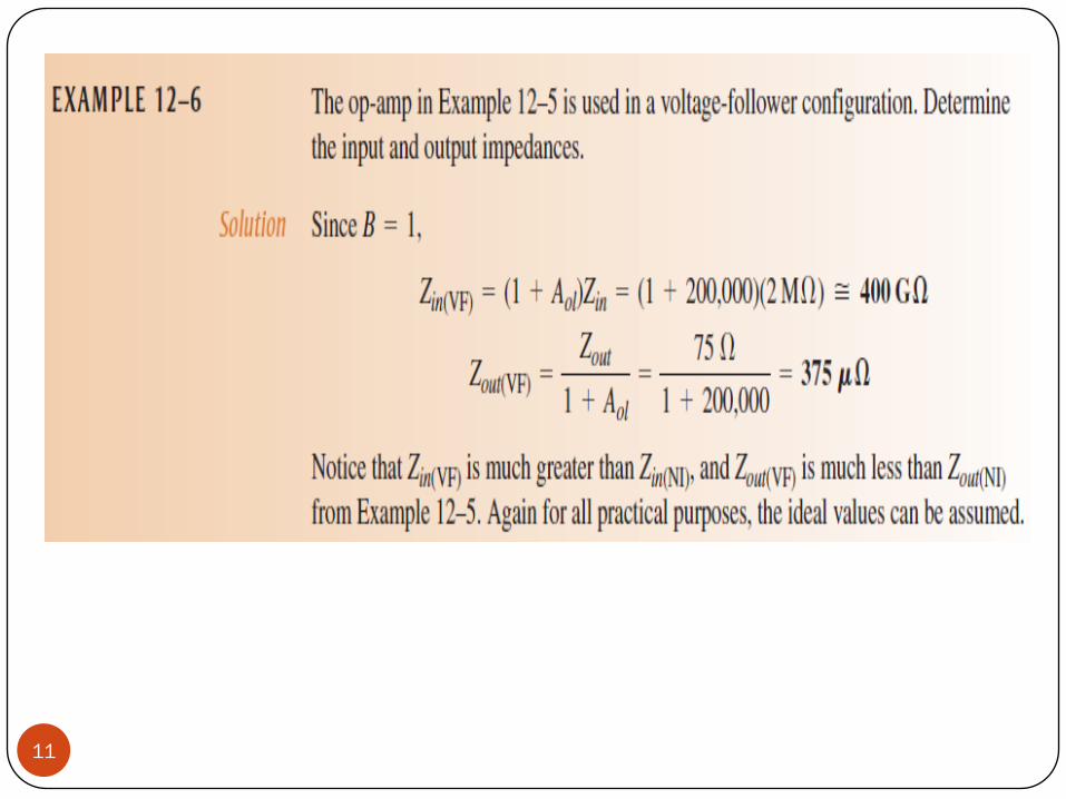
12-5 Effect of Negative FeedBack On OP-AMP Impedances Continue…
Voltage-Follower Impedances
Since a voltage follower is a special case of the non-inverting
amplifier configuration, the same impedance formulas are used
but with B= 1.
Notice that the voltage-follower input impedance is greater for
a given Aol and Zin than for the non-inverting amplifier
configuration with voltage-divider feedback circuit. Also the
output impedance is much smaller.
10
11

12-5 Effect of Negative FeedBack On OP-AMP Impedances Continue…
Impedances of an Inverting Amplifier
Input Impedance
The input impedance of an inverting amplifier can be developed with the
aid of figure 12-26.
The input signal is applied through a series resistor ,Ri , to inverting (-)
terminal.
The input impedance of an inverting amplifier is Zin (I) ≈ Ri
12

12-5 Effect of Negative FeedBack On OP-AMP Impedances Continue…
Impedances of an Inverting Amplifier
Output Impedance
As with a non-inverting amplifier, the output impedance of an inverting
amplifier is also decreased by the negative feedback, the expression is the
same as for the non-inverting case.
The output impedance of both the non-inverting and the inverting
amplifier configurations is very low; in fact it is almost zero in practical
cases.
13
14

15

12-6 Bias Current and Offset Voltage
The practical op-amp has small input bias currents typically
in nA range. Also small internal imbalances in the transistors
effectively produce a small offset voltage between the inputs.
Effect of an Input Bias Current
Figure 12-29 (a) next slide is an inverting amplifier with zero
input voltage.
Ideally the current through Ri is zero because the input voltage
is zero and the voltage at the inverting (-) terminal is zero.
The small input bias current, I1 is through Rf from the output
terminal.
I1 creates a voltage drop across Rf as indicated.
The positive side of Rf is the output terminal, thus the output
error voltage is + I1Rf when it should be zero16
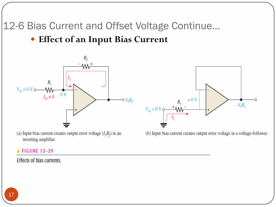
12-6 Bias Current and Offset Voltage Continue…
Effect of an Input Bias Current
17

12-6 Bias Current and Offset Voltage Continue…
Effect of an Input Bias Current
Figure 12-29 (b) previous slide is a voltage follower with zero
input voltage and a source resistance Rs .
Input bias current I1, produces a drop across Rs and creates an
output voltage error as shown.
The voltage at the inverting terminal decreases to -I1Rs because
the negative feedback tends to maintain a differential voltage of
zero as indicated.
Since the inverting terminal is connected directly to the output
terminal, the output error voltage is -I1Rs.
18

12-6 Bias Current and Offset Voltage Continue…
Effect of an Input Bias Current
Figure 12-30 is a non-inverting amplifier with zero input
voltage.
Ideally the voltage at the inverting terminal is also zero.
The input bias current I1, produces a voltage drop across Rf and
thus creates an output error voltage of I1Rf
19

12-6 Bias Current and Offset Voltage Continue…
Bias Current Compensation in aVoltage-Follower
The output error voltage due to bias current in a voltage-
follower can be significantly reduced by adding a resistor Rfequal to the source resistor Rs in the feedback path as shown in
figure 12-31 next slide.
The voltage drop created by I1 across the added resistor
subtracts from the -I2Rs output error voltage.
If I1= I2 , then the output volage is zero
Usually I1 does not equal I2 but even in this cases, the output
error voltage is reduced as follows because IOS is less than I2
20

12-6 Bias Current and Offset Voltage Continue…
Bias Current Compensation in aVoltage-Follower
21

12-6 Bias Current and Offset Voltage Continue…
Bias Current Compensation in Other Op-Amp
Configurations
Practical op-amp has very small finite input bias currents on both of
its inputs.
These two bias currents (I1 and I2) can produce a small dc output
voltage (VOUT(error) ) even when the input voltage is zero.
The easiest way to minimize this problem is by including a
compensating resistor Rc in series with the non-inverting input of a
non-inverting amplifier as shown in figure 12-32 (a) next slide.
The compensating resistor Rc value equals the parallel combination
of Ri and Rf.
Rc Provides high input impedance which will significantly reduce the
magnitudes of bias currents.
The inverting amplifier is similarly compensated shown in 12-32 (b)22

12-6 Bias Current and Offset Voltage Continue…
Bias Current Compensation in Other Op-Amp
Configurations
23

12-6 Bias Current and Offset Voltage Continue…
Effect of Input OffsetVoltage
Input OffsetVoltage Compensation
HOME READINGASSIGNMENT
24

12-7 Open-Loop Response
In this section, we will learn about the open-loop frequency
response and the open-loop phase response of an op-amp.
Open-loop responses relate to an op-amp with no external
feedback.
The frequency response indicates how the voltage gain changes
with frequency.
The phase response indicates how the phase shift between the
input and output signal changes with frequency.
The open-loop gain, like the β of a transistor, varies greatly from
one device to the next of the same type and cannot be dependent
upon to have a constant value.
25

12-7 Open-Loop Response Continue…
Voltage Gain is Frequency Dependent
Previously, all of the voltage gain expressions were based on the
midrange gain and were considered independent of the frequency.
The midrange open-loop gain of an op-amp extends from zero
frequency up to a critical frequency at which the gain is 3 dB less
than the midrange value.
Op-Amp are dc amplifiers ( no coupling capacitors between stages),
and therefore no lower critical frequency.
An open-loop response curve (Bode Plot) for a certain amplifier is
shown in figure 12-36 next slide.
Notice that the curve rolls off (decrease) at -20 dB per decade (-6
dB per octave).
The midrange gain is 200,000, which is 106 dB and the critical
(cutoff) frequency is approximately 10 Hz.26

12-7 Open-Loop Response Continue…
27

12-7 Open-Loop Response Continue…
3 dB Open-Loop Bandwidth
Generally the B.W equals the upper critical frequency minus the
lower critical frequency.
BW= fcu - fcl
Since fcl for an op-amp is zero, the B.W is simply equal to the upper
critical frequency.
BW= fcu
From now on, we will refer to fcu as simply fc ; and we will use open-
loop(ol ) or closed-loop (cl) subscript designators, for example, fc(ol).
28

12-7 Open-Loop Response Continue…
Unity-Gain Bandwidth
Notice in figure 12-36 that the gain steadily decreases to a point
where it is equal to unity ( 1 or 0 dB). The value of the frequency at
which this unity gain occurs is the unity-gain bandwidth designated fT fT = Aol BW = Aol fcu = Aol fc(ol)
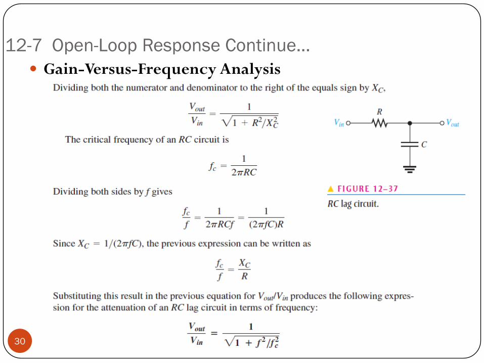
Gain-Versus-Frequency Analysis
The RC lag (low-pass) circuits within an op-amp are responsible for
the roll-off in gain as the frequency increases. From basic ac circuit
theory, the attenuation of an RC lag circuit such as in figure 12-37
next slide is expressed as
29
12-7 Open-Loop Response Continue…
Gain-Versus-Frequency Analysis
30

12-7 Open-Loop Response Continue…
Gain-Versus-Frequency Analysis
31

32

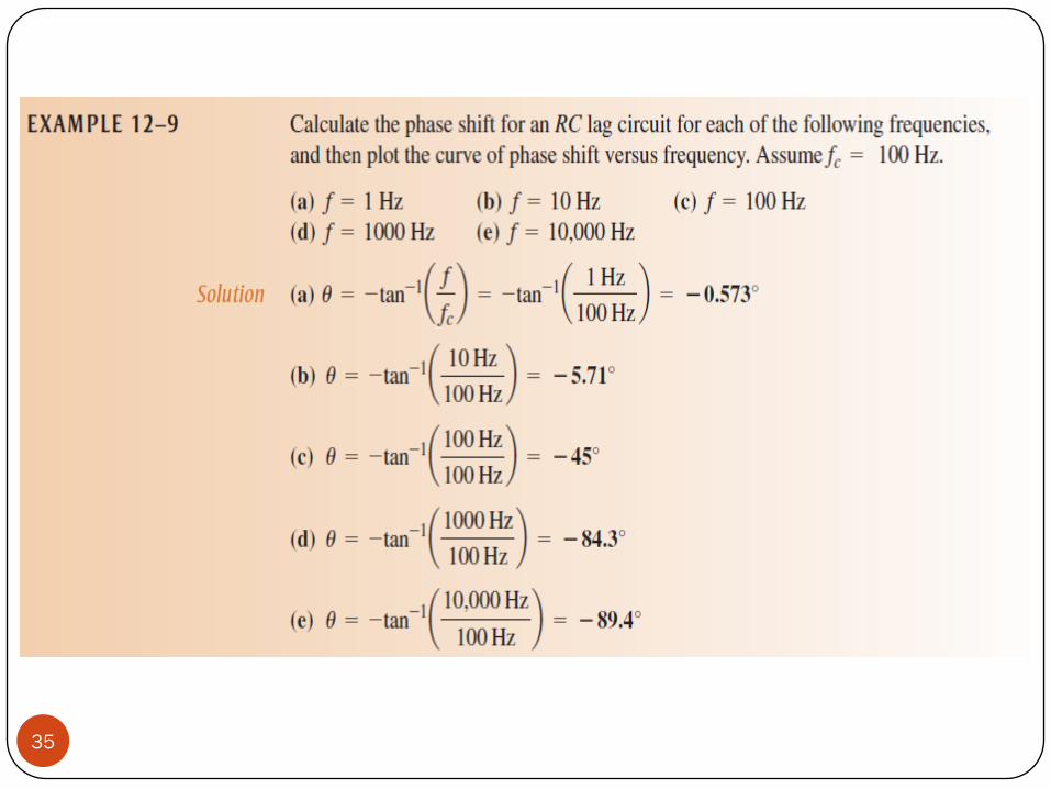
12-7 Open-Loop Response Continue…
Phase Shift
An RC circuit causes a propagation delay from input to output thus
creating a phase shift between the input signal and output signal.
An RC lag circuit such as found in an op-amp stage causes the output
signal voltage to lag the input as shown in figure 12-39. From basic
ac circuit theory, the phase shift θ is
33

12-7 Open-Loop Response Continue…
Phase Shift
34
35

36

12-7 Open-Loop Response Continue…
Complete Frequency Response
Previously an op-amp was assumed to have a constant roll-off of -20
dB/decade above its critical frequency. For most op-amps it is the
case.
However , the situation is more complex when IC op-amp may
consist of two or more cascaded amplifier stages.
The gain of each stage is frequency dependent and rolls off at -20
dB/decade above its critical frequency.
Therefore the total response of an op-amp is a composite of the
individual responses of the internal stages.
As an example, a three-stage op-amp is represented in figure 12-41
(a) next slide, the frequency response of each stage is shown in
figure 12-41(b), since gains are added so that the total op-amp
frequency response is shown in figure 12-41(c)37

38

12-7 Open-Loop Response Continue…
Complete Phase Response
In multistage amplifier, each stage contributes to the total phase lag.
Since each RC circuit can produce up to a -90˚ phase shift.
Therefore an op-amp with three internal stages can have a
maximum phase lag of -270˚.
The phase lag of each stage is less than-45˚ when the frequency is
below the critical frequency, equal to -45˚ at the critical frequency
and greater than -45˚ when the frequency is above critical
frequency.
The phase lags of the stages( three stages) of an-amp are added to
produce a total phase lag as follows
39

40

12-8 Closed-Loop Response
Op-Amps are normally used in a closed-loop configuration with
negative feedback in order to achieve precise control of the gain
and bandwidth.
Recall that the midrange gain (midrange open-loop gain) is
reduced by negative feedback. For a non-inverting amplifier
41

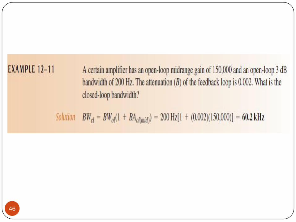
12-8 Closed-Loop Response Continue…
Effect of Negative Feedback on Bandwidth
The closed-loop critical frequency of an op-amp is
fc(cl)= fc(ol) (1+ BAol(mid))
This expression shows that the closed-loop critical frequency fc(cl) is
higher than the open-loop critical frequency fc(ol) by the factor
1+ BAol(mid).
BWc(cl) = BWc(ol)(1+ BAol(mid))
42
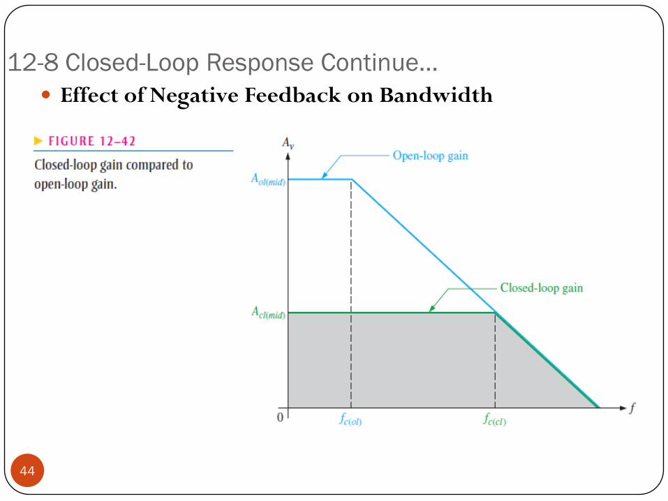
12-8 Closed-Loop Response Continue…
Effect of Negative Feedback on Bandwidth
Figure 12-42 next slide graphically illustrates the concept of closed-
loop response.
When the open-loop gain of an op-amp is reduced by negative
feedback, the bandwidth is increased.
The closed-loop gain is independent of the open-loop gain up to the
point of intersection of two gain curves.
This point of the intersection is the critical frequency fc(cl) for the
closed-loop response.
Notice that the closed-loop gain has the same roll-off rate as the open-
loop gain, beyond the closed-loop critical frequency.
43
12-8 Closed-Loop Response Continue…
Effect of Negative Feedback on Bandwidth
44

12-8 Closed-Loop Response Continue…
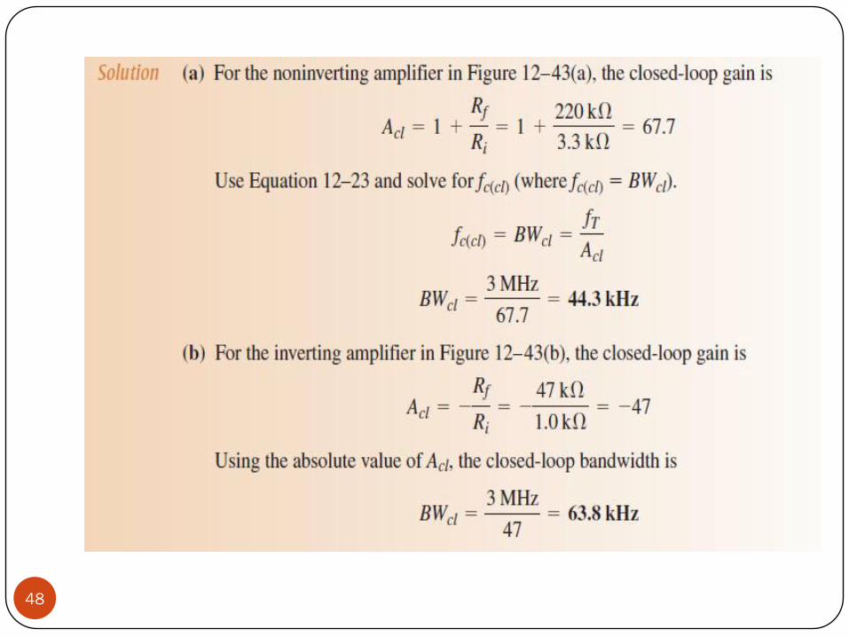
Gain-Bandwidth Product
An increase in closed-loop gain causes a decrease in the bandwidth and
vice versa.
This is true as long as the roll-off rate is fixed.
Unity-Gain Bandwidth
fT = Acl BWcl = Acl fcl = Acl fc(cl)
45
46

47
48