Embed Size (px)
Citation preview

VENUS INTERNATIONAL COLLEGE OF TECHNOLOGYBHOYAN RATHOD, GANDHINAGAR
A presentation on : Analog-to-Digital Converters.Name : Amitabh Shukla, Akshay Dudhagara
Enrolment no. : 12081011XXXX / 12081011XXXX
Branch : EC (5th Sem.)
Subject : Microcontroller and Interfacing
Guided by : Mihir Patel
What is ADC (Analog-to-Digital Converters)?Most of the quantities such as temperature, sound, etc. are in analog form.
These quantities are represented accurately in analog form but are difficult to process, store or transmit the analog signal because error gets introduced easily, due to noise.
Hence to reduce there errors it is always better to express these quantities in digital form.
For this purpose a ADC (Analog-to-Digital Converter) is necessary.
We have many ADC ICs like IC7109, ICL 7109, ADC 0808/0809.
Here we will only discuss about ADC 0808.
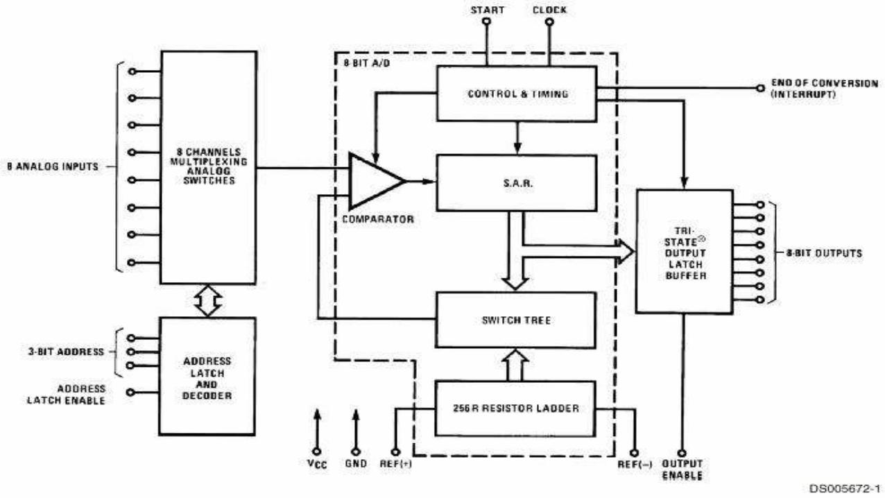
Principle of A to D Conversion in ADC 0808A/D converter uses successive approximation as the conversion technique.
The ADC0808 is a monolithic CMOS (Complementary Metal Oxide Conductor) device with an 8-bit analog-to-digital converter input, 8-channel multiplexer and microcontroller compatible control logic.
It includes 256 register voltage divider, a group of analog switches and successive approximation register (SAR).
As there are 8-analog channel, we can connect up to 8 analog inputs to this IC.
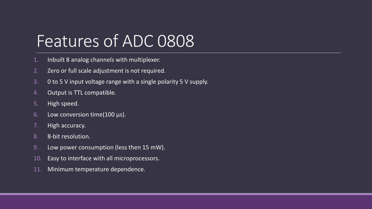
Features of ADC 08081. Inbuilt 8 analog channels with multiplexer.
2. Zero or full scale adjustment is not required.
3. 0 to 5 V input voltage range with a single polarity 5 V supply.
4. Output is TTL compatible.
5. High speed.
6. Low conversion time(100 µs).
7. High accuracy.
8. 8-bit resolution.
9. Low power consumption (less then 15 mW).
10. Easy to interface with all microprocessors.
11. Minimum temperature dependence.
Block Diagram of ADC 0808
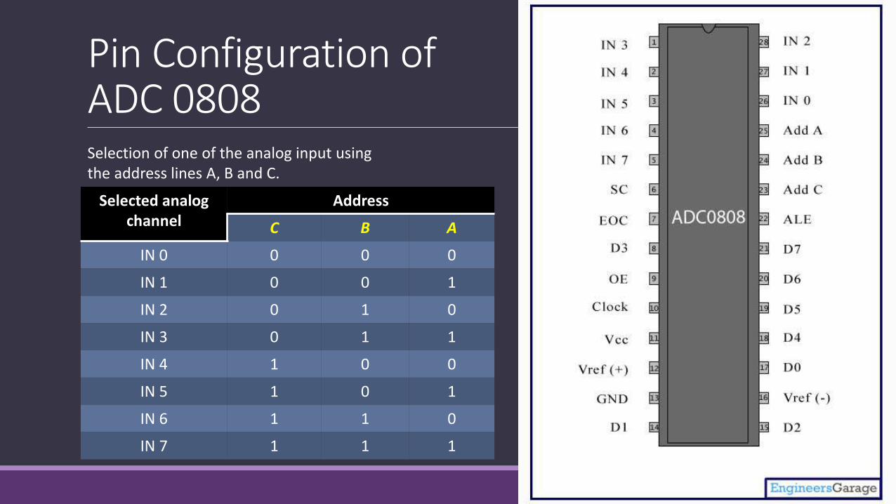
Pin Configuration ofADC 0808
Selected analogchannel
Address
C B A
IN 0 0 0 0
IN 1 0 0 1
IN 2 0 1 0
IN 3 0 1 1
IN 4 1 0 0
IN 5 1 0 1
IN 6 1 1 0
IN 7 1 1 1
Selection of one of the analog input usingthe address lines A, B and C.
Pin Configuration of ADC 0808i. Analog Input (IN 0 to IN 7)
ii. Address Pins A,B,C (Pin 25, 24, 23)
iii. Reference Voltage [VREF (+) and VREF (-)]
iv. ALE and Output Enable
v. Start (SOC) and EOC
vi. Data bits -- D0-D7
vii. CLK – Clock Input
Interfacing of ADC 0808 to 8051
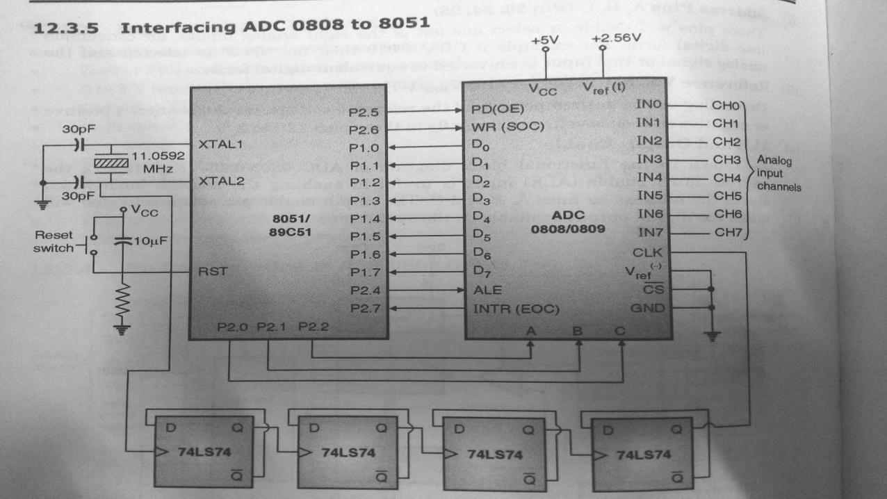
Interfacing of ADC 0808 to 8051ADC 0808 has eight input channels. Hence in order to select an input channel, it is essential to send 3 bit address on C, B and A inputs.
The address of the desired channel is sent to the address inputs through port pins P2.0, P2.1 and P2.2.
After 50 nS the address must be latched. It can be obtained by sending ALE signal. After 2.5 µS, SOC must be made high and then low to start the conversion.
To indicate end of conversion, EOC signal must be activated.
The 8051 pins P2.6 and P2.7 are connected to SOC and EOC pins of ADC 0808.
After the conversion is over, 8 bit digital data is present on D0 - D7 lines.
Algorithm Select an analog channel by provide bits to A, B, C.
Enable clock
Activate ALE with a low-to-high pulse.
Activate SC with a high-to-low pulse (start conversion). The conversion will begun on the falling edge of the start conversion pulse.
Monitor EOC Pin .After conversion this pin goes high.
Activate OE with a high-to-low pulse to read data output of the ADC chip.
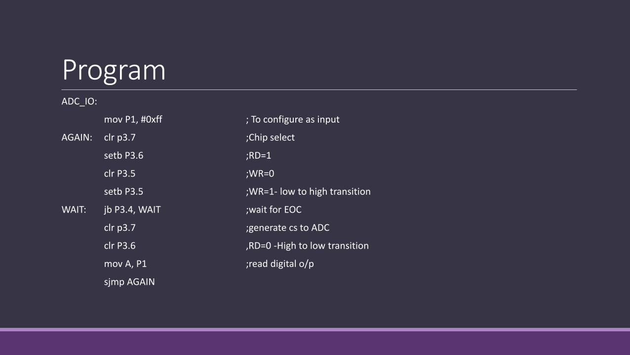
ProgramADC_IO:
mov P1, #0xff ; To configure as input
AGAIN: clr p3.7 ;Chip select
setb P3.6 ;RD=1
clr P3.5 ;WR=0
setb P3.5 ;WR=1- low to high transition
WAIT: jb P3.4, WAIT ;wait for EOC
clr p3.7 ;generate cs to ADC
clr P3.6 ,RD=0 -High to low transition
mov A, P1 ;read digital o/p
sjmp AGAIN

THANK YOU