Embed Size (px)
Citation preview

F.N.E.
S.C. JUN
Dept. of Mechanical Engineering

F.N.E.
S.C. JUN
Dept. of Mechanical Engineering
Range of conductivites exhibited by various materials

F.N.E.
S.C. JUN
Dept. of Mechanical Engineering
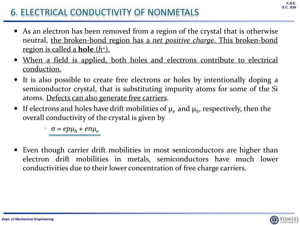
6. ELECTRICAL CONDUCTIVITY OF NONMETALS
All metals are good conductors because they have a very large number of conduction electrons free inside the metal.
Conductors are intimately identified with metals. It is more appropriate to view insulators as High resistivity (or low conductivity) materials.
6.1 SEMICONDUCTORS We know from classical physics (the kinetic molecular theory and Boltzmann
distribution) that all the atoms in the crystal are executing vibrations with a distribution of energies.
As the temperature increases, the distribution spreads to higher energies. Statistically some of the atomic vibrations will be sufficiently energetic to rupture a bond as indicated in Figure 12 a.
This releases and electron from the bond which is free to wander inside the crystal. The free electron can drift in the presence of an applied field; it is called a conduction electron.

F.N.E.
S.C. JUN
Dept. of Mechanical Engineering
6. ELECTRICAL CONDUCTIVITY OF NONMETALS
Figure 12
(a) Thermal vibrations of the atoms rupture a bond and release a free electron into the
crystal. A hole is left in the broken bond which has an effective positive charge.
(b) An electron in a neighboring bond can jump and repair this bond and thereby create a
hole in its original site; the hole has been displaced.
(c) When a field is applied both holes and electrons contribute to electrical conduction.
F.N.E.
S.C. JUN
Dept. of Mechanical Engineering
6. ELECTRICAL CONDUCTIVITY OF NONMETALS
As an electron has been removed from a region of the crystal that is otherwise neutral, the broken-bond region has a net positive charge. This broken-bond region is called a hole (h+).
When a field is applied, both holes and electrons contribute to electrical conduction.
It is also possible to create free electrons or holes by intentionally doping a semiconductor crystal, that is substituting impurity atoms for some of the Si atoms. Defects can also generate free carriers.
If electrons and holes have drift mobilities of µe and µh, respectively, then the overall conductivity of the crystal is given by
σ = epμh + enμe
Even though carrier drift mobilities in most semiconductors are higher than electron drift mobilities in metals, semiconductors have much lower conductivities due to their lower concentration of free charge carriers.

F.N.E.
S.C. JUN
Dept. of Mechanical Engineering
6. ELECTRICAL CONDUCTIVITY OF NONMETALS
6.2 IONIC CRYSTALS AND GLASSES Crystal defects in an ionic crystal lead to mobile charges that can contribute to
the conduction process.
Figure 13 Possible contribution to the conductivity of ceramic and glass insulators.
(a) Possible mobile charges in a ceramic.
(b) An Na+ ion in the glass structure diffuses and therefore drifts in the direction of the field.

F.N.E.
S.C. JUN
Dept. of Mechanical Engineering
6. ELECTRICAL CONDUCTIVITY OF NONMETALS
Many solids have interstitial impurities which are often ionized or charged. These interstitial ions can jump, i.e., diffuse, from one interstitial site to another and hence drift by diffusion in the presence of a field.
Aided by the field, the Na+ can jump from one interstice to a neighboring interstice along the field and thereby drift in the glass and contribute to current conduction. The conduction process is then essentially field-directed diffusion.
Conductivity σ of the material depends on all the conduction mechanisms with each species of charge carrier making a contribution, so it is given by
σ = 𝑞𝑖𝑛𝑖μ𝑖 [4]
ni is the concentration, qi is the charge carried by the charge carrier species of type i (for electrons and holes qi = e), and µi is the drift mobility of these carriers.
σ = σ0 expEσ
kT
Where Eσ is the activation energy for conductivity.

F.N.E.
S.C. JUN
Dept. of Mechanical Engineering
Figure 14 shows examples of the temperature dependence of conductivity for various high-resistivity solids: oxide ceramics, glasses, and polymers. When Equation [4] is plotted as log (σ) versus 1/T, the result is a straight line with a negative slope that indicates the activation energy Eσ.
6. ELECTRICAL CONDUCTIVITY OF NONMETALS
Figure 14 Conductivity versus reciprocal temperature for various low-conductivity
solids SOURCE: Data selectively combined from numerous sources.

F.N.E.
S.C. JUN
Dept. of Mechanical Engineering
The currents I1 in the solid and I2 in hollow cylinders sum to I.
I1 flowing in the inner conductor is threaded (or linked) by both B1 and B2.
7. SKIN EFFECT: HF RESISTANCE OF A CONDUCTOR
Figure 15 Illustration of the skin effect. A hypothetical cut
produces a hallow outer cylinder and a solid inner cylinder.
Cut is placed where it would give equal current in each
section. The two sections are in parallel so that the currents
in (b) and (c) sum to that in (a).
I1
I2
Figure 16 At high frequencies,
the core region exhibits more
inductive impedance than the
surface region, and the current
flows in the surface region of
conductor defined
approximately
by the skin depth, δ.

F.N.E.
S.C. JUN
Dept. of Mechanical Engineering
Recall that inductance is defined as the total magnetic flux threaded per unit current. Consequently, and ac current will prefer paths near the surface where the inductive impedance is smaller. As the frequency increases, the current is confined more and more to the surface region.
Most of the current flows in a surface region of depth δ, called the skin depth.
In the central region, the current will be negligibly small. The skin depth will obviously depend on the frequency ω.
δ = 1
1
2ωσμ
Where ω is the angular frequency of the current, σ is the conductivity (σ is constant from dc up to ~1014 Hz in metals).
µ is the magnetic permeability of the medium, which is the product of the absolute (free space) permeability µ0 and the relative permeability µr.
7. SKIN EFFECT: HF RESISTANCE OF A CONDUCTOR

F.N.E.
S.C. JUN
Dept. of Mechanical Engineering
With the skin depth known, the effective cross-sectional area is given approximately by
A = πa2 – π(a – δ)2 ≈ 2πaδ
Where δ2 is neglected (δ ≪ a). The ac resistance rac of the conductor per unit length is.
rac = ρA
≈ ρ
2πaδ
Where ρ is the ac resistivity at the frequency of interest, which for all practical purposes is equal to the dc resistivity of the metal.
As ω increases, δ decreases, by virtue of δ ∝ ω-1/2 and, as a result, rac increases.
The skin effect arises because the magnetic field of the ac current in the conductor restricts the current flow to the surface region within a depth of δ < a.
7. SKIN EFFECT: HF RESISTANCE OF A CONDUCTOR

F.N.E.
S.C. JUN
Dept. of Mechanical Engineering
Any dimension of the specimen is much larger than the mean free path for electron scattering. In such cases resistivity is determined by scattering from lattice vibrations and, if significant, scattering from various impurities and defects in the crystal.
8. THIN METAL FILMS
8.1 CONDUCTION IN THIN METAL FILMS
In a highly polycrystalline sample the conduction electrons are more likely to be scattered by grain boundaries than by other processes as depicted in Figure 17.
The conduction electron is free within a grain, but becomes scattered at the grain boundary. Its mean free path lgrains is therefore roughly equal to the average grain size d.
8.2 RESISTIVITY OF THIN FILMS
Figure 17
(a) Grain boundaries cause scattering of the
electron and therefore add to the
Resistivity by the Matthiessen’s rule.
(b) For a very grainy solid, the electron is
scattered from grain boundary to grain
boundary and the mean free path is
approximately equal to the mean grain
diameter.

F.N.E.
S.C. JUN
Dept. of Mechanical Engineering
8. THIN METAL FILMS
If λ = lcrystal is the mean free path of the conduction electrons in the single crystal (no grain boundaries).
1
l = 1
lcrystal +
1
lgrains =
1
λ +
1
𝑑
The resistivity is inversely proportional to the mean free path which means that the resistivity of the bulk single crystal ρcrystal ∝ 1/λ and the resistivity of the polycrystalline sample ρ ∝ 1/l. Thus,
ρ
ρcrystal = 1 +
λ
𝑑 With a smaller grain diameter d
Figure 18 Conduction in thin films
may be controlled by scattering from
the surfaces

F.N.E.
S.C. JUN
Dept. of Mechanical Engineering
8. THIN METAL FILMS
There is a possibility that the electron may be totally reflected back at a grain boundary (bounce back). Suppose that the probability of reflection at a grain boundary is R.
𝛽 = λ
𝑑
R1 − R
For copper, typical R values are 0.24 to 0.40, and R is somewhat smaller for Al.
Assume that the scattering from the surface is inelastic; that is, the electron loses the grained velocity from the field.
The direction of the electron after the scattering process is independent of the direction before the scattering process. This type of scattering is called nonspecular.
The mean free path lsurf of the electron will depend on its direction right after the scattering.
Figure 19 The mean free path of the
electron depends on the angle after
scattering.

F.N.E.
S.C. JUN
Dept. of Mechanical Engineering
8. THIN METAL FILMS
It therefore takes two collisions to randomize the velocity, which means that the effective mean free path must be twice as long, that is 2D/cos θ.
Overall mean free path l for calculating the resistivity we must use Matthiessen’s rule. If λ is the mean free path of the conduction electrons in the bulk crystal (no surface scattering), then
1
l = 1
λ +
1
lsuf =
1
λ +
cos θ2D
Average for all possible θ values per scattering, θ from –π /2 to +π /2.
λl = 1 +
λπD
The resistivity of the bulk crystal is ρbulk ∝ 1/λ, and the resistivity of the film is ρ ∝ 1/l. Thus
ρ
ρbulk = 1 +
1π
λD
ρ
ρbulk ≈ 1 +
3λ8D(1 – P)
Dλ
> 0.3 [5]

F.N.E.
S.C. JUN
Dept. of Mechanical Engineering
8. THIN METAL FILMS
For elastic or specular scattering P = 1 and there is no change in the resistivity.
For p = 0, Equation [5] predicts ρ/ρbulk ≈ 1.20 for roughly D ≈ 1.9λ or a thickness D ≈ 75 nm for Cu for which λ ≈ 40 nm. The value of p depends on the film preparation method.
It is generally very difficult to separate the effects of surface and grain boundary scattering in thin poly crystalline films; the contribution from grain boundary scattering is likely to exceed that from the surfaces. In any event, both contributions, by Matthiessem’s general rule, increase the overall resistivity.
In this case, annealing (heat treating) the films to reduce the polycrystallinity does not significantly affect the resistivity because ρfilm is controlled primarily by surface scattering and is given by Equation [5].

F.N.E.
S.C. JUN
Dept. of Mechanical Engineering
(a) film of the Cu polycrystalline films vs. reciprocal mean grain size (diameter), 1/d. Film
thickness D = 250 nm - 900 nm does not affect the resistivity. The straight line is film = 17.8
n m + (595 n m nm)(1/d),
(b) film of the Cu thin polycrystalline films vs. film thickness D. In this case, annealing (heat
treating) the films to reduce the polycrystallinity does not significantly affect the resistivity
because film is controlled mainly by surface scattering.
|SOURCE: Data extracted from (a) S. Riedel et al, Microelec. Engin. 33, 165, 1997 and (b). W. Lim et al,
Appl. Surf. Sci., 217, 95, 2003)
Figure 20

F.N.E.
S.C. JUN
Dept. of Mechanical Engineering
Three levels of interconnects in a flash memory chip.
Different levels are connected through vias.
|SOURCE: Courtesy of Dr. Don Scansen,
Semiconductor Insights, Kanata, Ontario, Canada

F.N.E.
S.C. JUN
Dept. of Mechanical Engineering
9. INTERCONNECTS IN MICROELECTRONICS
Aluminum and Al alloys, or Al silicides, have been the workhouse of the interconnects, but today’s fast chips rely on copper interconnects.
First, copper has a resistivity that is about 40 percent lower than that of Al.
High-transistor-density chips in which various voltages are switched on and off limits the speed of operation is the RC time constant.
The time constant that is involved in charging and discharging the capacitance between the interconnects.
Input capacitance of the transistor; usually the former dominates. (advantages)
The RC is substantially reduced with Cu replacing Al so that the chip speed is faster.
The second advantage is that a lower overall interconnect resistance leads to a lower power consumption, lower I2R.
The third advantage is that copper has superior resistance to electro-migration, a process in which metal atoms are forced to migrate by a large current density. Such electro-migration can eventually lead to a failure of the interconnect.