www.magntek.com.cn| Magnetic Tech Makes Magic Change Rev 1.0 2019.07
Zero Latency Magnetic Angle Position Sensor IC
MT6825
Features and Benefits■ Based on advanced AMR Technology with
0~360° Full Range Angle Sensing
■ 18 bit Core Resolution
■ Maximum Rotation Speed 25,000 RPM
■ Output Propagation Delay <2 us
■ -40~125℃ Industry Operating Temperature
Range
■ Independent Output Interface: ABZ, UVW,
PWM and SPI
■ Incremental ABZ Resolution 1~4096 Pulses
per Revolution User Programmable
■ UVW Output Resolution 1~16 Pole-Pairs
per Revolution User Programmable
■ TSSOP-16 Package
1
General Description
The MagnTek rotary position sensor
MT6825 is an IC based on advanced AMR
technology. A rotating magnetic field in the
x-y sensor plane delivers two sinusoidal
output signals which indicating the angle
(α) between the sensor and the magnetic
field direction.
The sensor is only sensitive to the magnetic
field direction in x-y plane as the sensing
element output is specially designed to be
independent from the magnet field strength.
This allows the device to be less sensitive to
magnet variations, stray magnetic fields, air
gap changes and off-axis misalignment.
The incremental ABZ output mode is
available in this sensor series, making the
chip suitable to replace various optical
encoders. The maximum resolution is 16384
steps or 4096 pulses per revolution
A standard SPI (3-Wire or 4-Wire) interface
allows a host microcontroller to read out
the 18-bit absolute angle position data
from MT6825. The absolute angle position
is also provided as a 12bit PWM output.
Applications
■ Absolute Angle Position Sensor
■ BLDC Motor Control
■ Servo Motor Control
■ Stepping Motor Control
■ Optical Encoder Replacement
6 8 2 5
9 0 8
www.magntek.com.cn| Magnetic Tech Makes Magic Change Rev 1.0 2019.07
MT6825
2
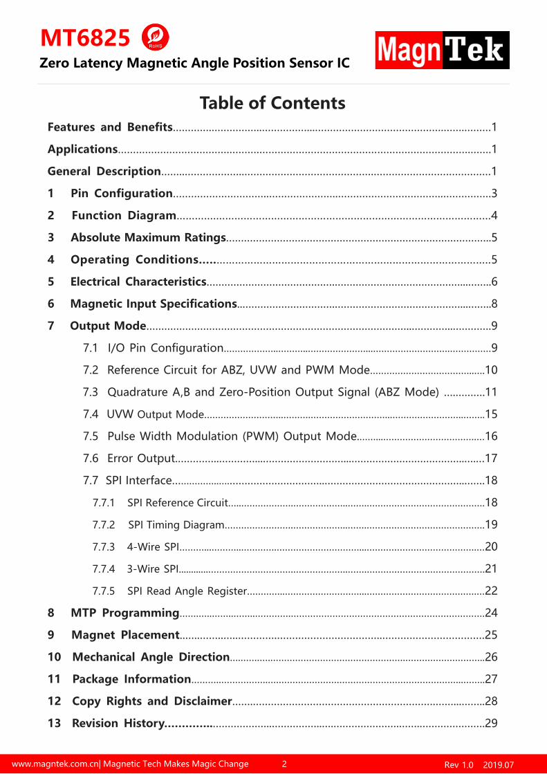
Table of ContentsFeatures and Benefits………….……………..……………...…………………………………….…….………1
Applications……………………………….……….…………………………………………………………….…….1
General Description……..………………..…………………………………….…………………………………1
1 Pin Configuration…………………………..…………………..……………………………..…………….3
2 Function Diagram………….………………………………………………………………………………4
3 Absolute Maximum Ratings……………………………………………………………………………..5
4 Operating Conditions…..……………………………………………………………………………..5
5 Electrical Characteristics…………………………………….……………………………………...……..6
6 Magnetic Input Specifications..………………………….……………………………………...……..8
7 Output Mode……………………………………………………………………………..…………..………….9
7.1 I/O Pin Configuration………………..………..…………………...……………………….……………9
7.2 Reference Circuit for ABZ, UVW and PWM Mode………………………………..….10
7.3 Quadrature A,B and Zero-Position Output Signal (ABZ Mode) ….……….11
7.4 UVW Output Mode………………………..……….………………………...……………………..……..15
7.5 Pulse Width Modulation (PWM) Output Mode.……...…………………………….…16
7.6 Error Output.…………..…………...………………………...………………………………..….…17
7.7 SPI Interface……………..….…………………………..………………………………………..…….18
7.7.1 SPI Reference Circuit…..……………….………………..…….…………………………………….18
7.7.2 SPI Timing Diagram…………………….………………..…….…………………………………….19
7.7.3 4-Wire SPI………...………..………….…………………………...………………………………….…20
7.7.4 3-Wire SPI............………………………….………………..…….…………………………………….21
7.7.5 SPI Read Angle Register…………..………………………...………………………………….…22
8 MTP Programming…….…..……..……..………….…………………………………………………………….24
9 Magnet Placement..…..……..…..………….……………………………..…………………………….25
10 Mechanical Angle Direction….…….….………………………………………….………………………..26
11 Package Information………..……………..….………………….……………………………………...……..27
12 Copy Rights and Disclaimer…….…………………………………………………….……...……..28
13 Revision History…………..………………..……………..….………………….…….………………….29
Zero Latency Magnetic Angle Position Sensor IC

www.magntek.com.cn| Magnetic Tech Makes Magic Change Rev 1.0 2019.07
MT6825
1. Pin Configuration
3
Figure 1: Pin Configuration of MT6825(TSSOP-16) Package
Name # Type Description
U 1 Digital Output Incremental Signal U or –A
V 2 Digital Output Incremental Signal V or –B
W 3 Digital Output Incremental Signal W or -Z
HVPP 4 Power Supply MTP Programming Supply. If Do Not Use, Connect to VSS.
MISO 5 Digital Output SPI Data, Slave Output Master Input
MOSI 6 Digital Input/OutputSPI Data, Master Output Slave Input. At 3-Wire Mode It is a
Bi-Direction Input-Output Pin
SCK 7 Digital Input SPI Clock
CSN 8 Digital Input SPI Select
VDD 9 Power Supply 3.3~5.0V Power Supply
OUT 10 Digital Output PWM Output
TEST 11 Digital Input Test Pin
VSS 12 Power Supply Ground
ERROR 13 Digital Output Error Output
Z 14 Digital Output Incremental Signal Z
B 15 Digital Output Incremental Signal B
A 16 Digital Output Incremental Signal A
Part Number Description
MT6825GT TSSOP-16 Package, Tube Pack (60 Pcs/Tube) or Tape & Reel Pack (3000 Pcs/Reel)
Family Members
Pin List
*TSSOP-16 Reflow Sensitivity Classification: MSL-3
1 8
16 915 14 13 12 11 10
2 3 4 5 6 7
Sensing Center atGeometry Center
Zero Latency Magnetic Angle Position Sensor IC
www.magntek.com.cn| Magnetic Tech Makes Magic Change Rev 1.0 2019.07
MT6825
4
2. Functional Diagram
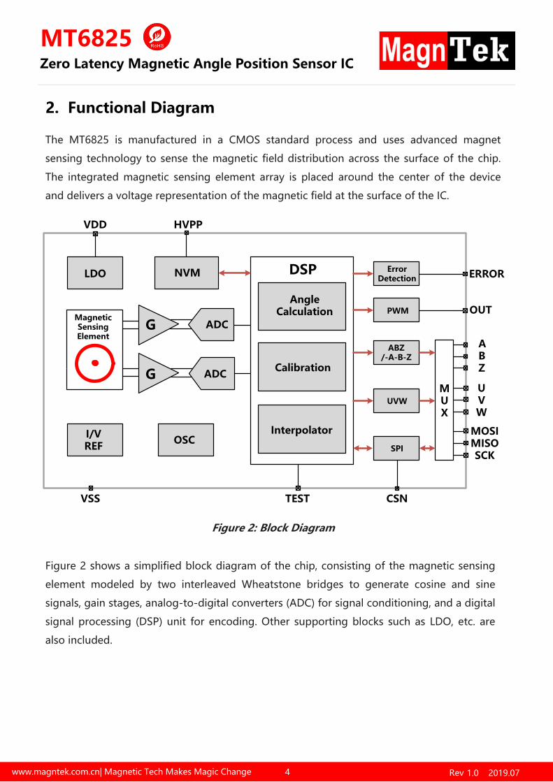
Figure 2: Block Diagram
The MT6825 is manufactured in a CMOS standard process and uses advanced magnet
sensing technology to sense the magnetic field distribution across the surface of the chip.
The integrated magnetic sensing element array is placed around the center of the device
and delivers a voltage representation of the magnetic field at the surface of the IC.
Figure 2 shows a simplified block diagram of the chip, consisting of the magnetic sensing
element modeled by two interleaved Wheatstone bridges to generate cosine and sine
signals, gain stages, analog-to-digital converters (ADC) for signal conditioning, and a digital
signal processing (DSP) unit for encoding. Other supporting blocks such as LDO, etc. are
also included.
Zero Latency Magnetic Angle Position Sensor IC
G
G
ADC
ADC
DSPLDO
Calibration
NVM
ABZ/-A-B-Z
PWM
VDD HVPP
ABZ
UVW
OUT
CSN
MUX
OSCSPI
UVW
VSS
Angle Calculation
Interpolator
Magnetic Sensing Element
MOSIMISO SCK
Error Detection ERROR
I/V REF
TEST

www.magntek.com.cn| Magnetic Tech Makes Magic Change Rev 1.0 2019.07
Zero Latency Magnetic Angle Position Sensor IC
MT6825
5
3. Absolute Maximum Ratings (Non-Operating)
Parameter Min. Max. Unit Notes
DC Voltage at Pin VDD -0.5 6.5 V
DC Voltage at Pin HVPP -0.5 8 V
Terminal Voltage at Input
and Output Pins-0.5 VDD V
ABZ, UVW, MISO, MOSI,
SCK, TEST, ERROR
Output Current at Output Pins -20 20 mAABZ, UVW, ERROR,
MISO, MOSI
Storage Temperature -55 150 ℃
Electrostatic Discharge (CDM) - ±1.0 KV
Electrostatic Discharge (HBM) - ±3.0 KV
Stresses beyond those listed under “Absolute Maximum Ratings” may cause permanent
damage to the device. These are stress ratings only. Functional operation of the device at
these or any other conditions beyond those indicated under “Operating Conditions” is
not implied. Exposure to absolute maximum rating conditions for extended periods may
affect device reliability.
4. Operating Conditions
Parameter Min. Max. Unit
DC Voltage at Pin VDD 3.0 5.5 V
DC Voltage at Pin HVPP (If Used) 6.75 7.25 V
Magnetic Flux Density Range 30 1,000 mT
Rotation Speed - 25,000 RPM
Operating Temperature -40 125 ℃

www.magntek.com.cn| Magnetic Tech Makes Magic Change Rev 1.0 2019.07
Zero Latency Magnetic Angle Position Sensor IC
MT6825
6
5. Electrical Characteristics
Operation conditions: Ta=-40 to 125℃, VDD=3.0~5.5V unless otherwise noted.
Symbol Parameter Conditions/Notes Min. Typ. Max. Unit
VDD Supply Voltage - 3.0 3.3~5.0 5.5 V
HVPP Supply Voltage - 6.75 7.0 7.25 V
Idd Supply Current - 5 10 15 mA
LSB Resolution (ABZ Mode) N Steps per Cycle - 360°/N - °
INL Integral Non-Linearity Note (1) - ±0.5 ±1.0 °
DNLDifferential Non-Linearity (ABZ Mode), Figure 3
@2500 PPR - ±0.01 - °
TN Transition Noise (ABZ Mode) 25℃ - 0.005 - °rms
Hyst Hysteresis (ABZ Mode) - 0.022 - °
TPwrUp Power-Up Time VDD Ramp<10us - 16 - ms
TDelay Propagation Delay - 1 3 us
PWM Output Characteristics Conditions/Notes Min. Typ. Max. Unit
FPWM PWM Frequency Programmable - 971.1/485.6 - Hz
TRise Rising Time CL=1nF - - 1 us
TFall Falling Time CL=1nF - - 1 us
Note (1): The typical error value can be achieved at room temperature and with no off-axis
misalignment error. The maximum error value can be achieved over operation temperature range,
at maximum air gap and with worst-case off-axis misalignment error.

www.magntek.com.cn| Magnetic Tech Makes Magic Change Rev 1.0 2019.07
Zero Latency Magnetic Angle Position Sensor IC
MT6825
7
Digital I/O Characteristics (Push-Pull Type in Normal Mode)
Symbol Parameter Conditions/Notes Min. Typ. Max. Unit
VIH High Level Input Voltage - 0.7*VDD - - V
VIL Low Level Input Voltage - - - 0.3*VDD V
VOH GPIO Output High Level Push-Pull (Iout=2mA) VDD-0.25 - - V
VOL GPIO Output Low Level Push-Pull (Iout=2mA) - - 0.25 V
ILK Input Leakage Current CSN (Build-in Pull-up) -100 - 1 uA
Figure 3: Drawing Illustration INL, DNL and TN (for 10 bit case)

www.magntek.com.cn| Magnetic Tech Makes Magic Change Rev 1.0 2019.07
Zero Latency Magnetic Angle Position Sensor IC
MT6825
8
6. Magnetic Input Specifications
Operation conditions: Ta=-40 to 125℃, VDD=3.0~5.5V unless otherwise noted, two-pole
cylindrical diametrically magnetized source.
Symbol Parameter Conditions/Notes Min. Typ. Max. Unit
Dmag Diameter of Magnet
Recommended Magnet:
Ø10mm x 2.5mm for
Cylindrical Magnets
- 10 - mm
Tmag Thickness of Magnet - - 2.5 - mm
BpkMagnetic Input Field
AmplitudeMeasure at the IC Surface 30 - 1,000 mT
AG Air GapMagnetic to IC Surface
Distance- - 3.0 mm
RS Rotation Speed - - 25,000 RPM
DISP Off Axis Misalignment
Misalignment Error
Between Sensor Sensing
Center and Magnet Axis
(See Figure 4)
- - 0.3 mm
TCmag1 Recommended Magnet
Material and Temperature
Drift Coefficient
NdFeB (Neodymium Iron
Boron)- -0.12 -
%/℃TCmag2 SmCo (Samarium Cobalt) - -0.035 -
Figure 4: Magnet Arrangement
Air Gap
Off-axis Misalignment
N S

www.magntek.com.cn| Magnetic Tech Makes Magic Change Rev 1.0 2019.07
Zero Latency Magnetic Angle Position Sensor IC
MT6825
9
7. Output Mode
The MT6825 provides ABZ, UVW and PWM signals at output pins, and also 18-bit absolute
angle position data could be transferred by SPI interface (Both 3-Wire and 4-Wire modes).
7.1 I/O Pin Configuration
Pin# 3-Wire SPI 4-Wire SPI ABZ+UVW+PWM ABZ Differential
1 - - U -A
2 - - V -B
3 - - W -Z
5 - MISO - -
6 SDAT MOSI - -
7 SCK SCK - -
10 OUT(PWM) OUT(PWM) OUT(PWM) OUT(PWM)
14 - - Z Z
15 - - B B
16 - - A A
I/O Pin Configuration
For TSSOP-16 package, ABZ (Single-end or differential), UVW, PWM and SPI Interface are
configured as below table.

www.magntek.com.cn| Magnetic Tech Makes Magic Change Rev 1.0 2019.07
Zero Latency Magnetic Angle Position Sensor IC
MT6825
10
Figure 5: ABZ, UVW and PWM Output Reference Circuit w/o MTP Programming
7.2 Reference Circuit for ABZ, UVW and PWM Mode
Figure 6: ABZ, UVW and PWM Output Reference Circuit w/i MTP Programming
VDD
1 8
16 915 14 13 12 11 10
2 3 4 5 6 7
TVS(6V)
PWM
-A -B -Z
0.1uf
NC NC NC NC
A B Z Erro
r
VDD
1 8
16 915 14 13 12 11 10
2 3 4 5 6 7
TVS(6V)
PWM
U V W NC NC NC NC
A B Z Erro
r 0.1uf
VDD
1 8
16 915 14 13 12 11 10
2 3 4 5 6 7
TVS(6V)
PWM
-A -B -Z
A B Z Erro
r
VDD
1 8
16 915 14 13 12 11 10
2 3 4 5 6 7
TVS(6V)
PWM
U V W
0.1uf
MIS
O
MO
SI
SCK
CSN
A B Z Erro
r
HVPP
1ufHVPP
1uf
MIS
O
MO
SI
SCK
CSN
0.1uf
www.magntek.com.cn| Magnetic Tech Makes Magic Change Rev 1.0 2019.07
Zero Latency Magnetic Angle Position Sensor IC
MT6825
11
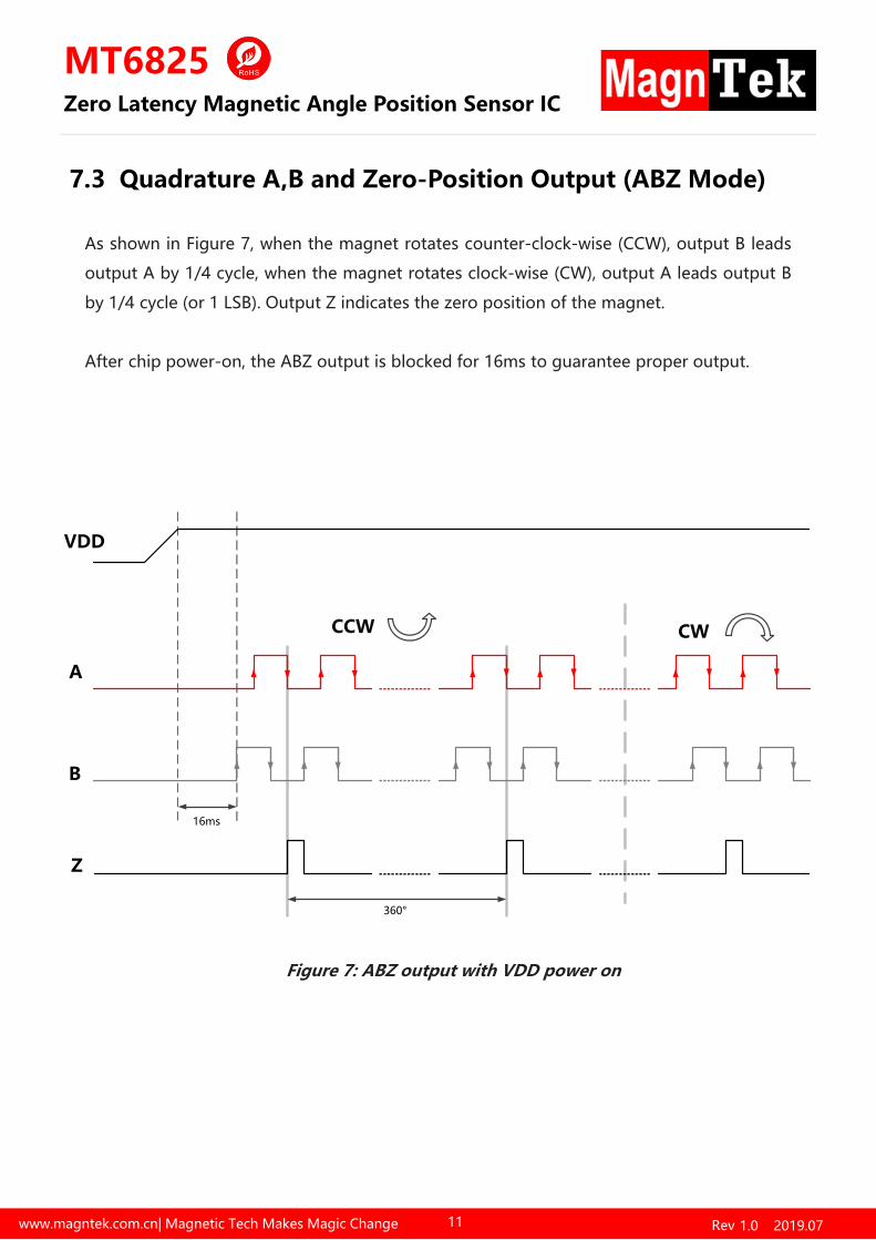
7.3 Quadrature A,B and Zero-Position Output (ABZ Mode)
As shown in Figure 7, when the magnet rotates counter-clock-wise (CCW), output B leads
output A by 1/4 cycle, when the magnet rotates clock-wise (CW), output A leads output B
by 1/4 cycle (or 1 LSB). Output Z indicates the zero position of the magnet.
After chip power-on, the ABZ output is blocked for 16ms to guarantee proper output.
Figure 7: ABZ output with VDD power on
A
Z
CCW
B
360°
VDD
CW
16ms
www.magntek.com.cn| Magnetic Tech Makes Magic Change Rev 1.0 2019.07
Zero Latency Magnetic Angle Position Sensor IC
MT6825
12
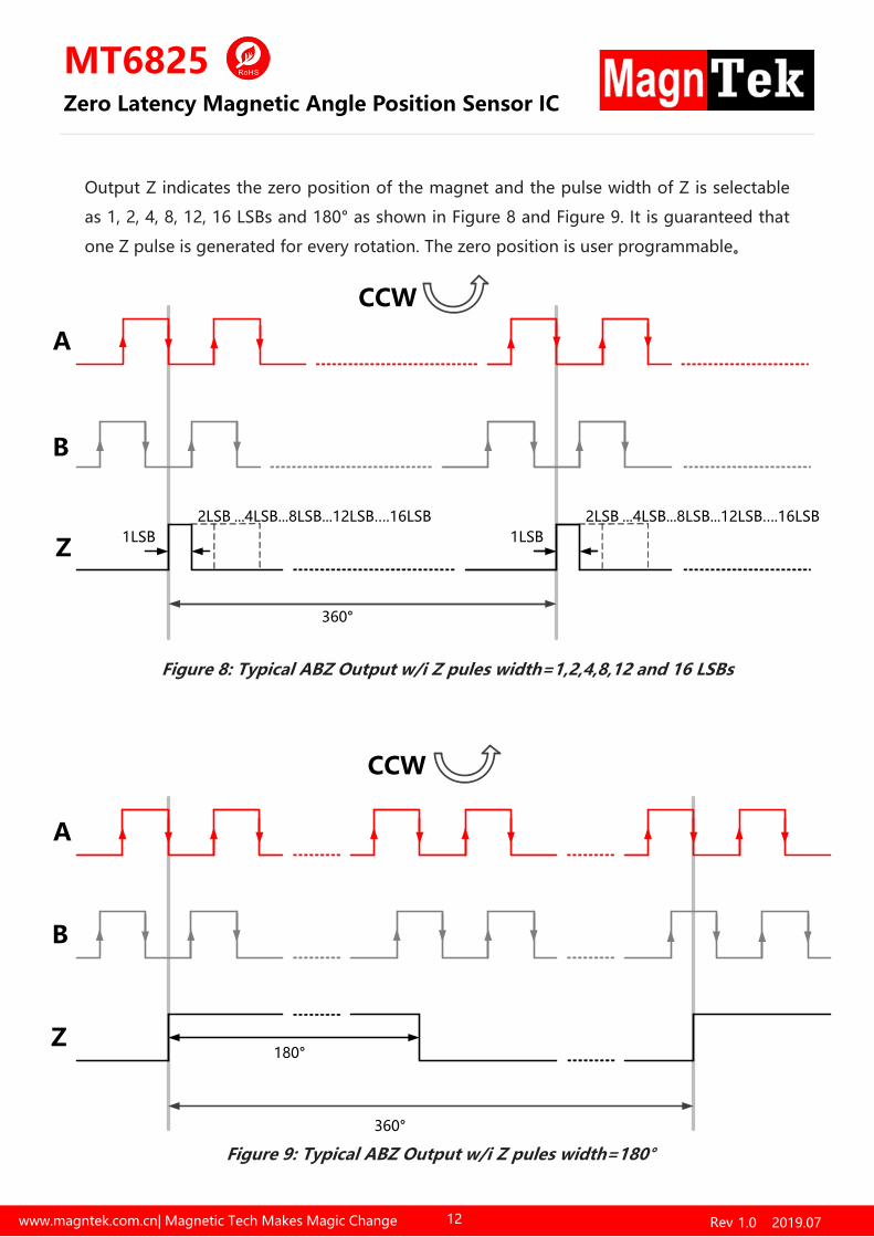
Output Z indicates the zero position of the magnet and the pulse width of Z is selectable
as 1, 2, 4, 8, 12, 16 LSBs and 180° as shown in Figure 8 and Figure 9. It is guaranteed that
one Z pulse is generated for every rotation. The zero position is user programmable。
Figure 8: Typical ABZ Output w/i Z pules width=1,2,4,8,12 and 16 LSBs
Figure 9: Typical ABZ Output w/i Z pules width=180°
A
Z 1LSB
CCW
B
2LSB ...4LSB...8LSB...12LSB….16LSB
360°
A
Z
CCW
B
360°
180°
1LSB2LSB ...4LSB...8LSB...12LSB….16LSB

www.magntek.com.cn| Magnetic Tech Makes Magic Change Rev 1.0 2019.07
Zero Latency Magnetic Angle Position Sensor IC
MT6825
13
ABZ resolution is user programmable from 1~4096 PPR. The relationship between binary
bits, LSBs and PPR resolution of ABZ output are shown in Figure 10 and Figure 11.
Figure 11: ABZ Output Resolution=2500 PPR
Figure 10: ABZ Output Resolution=10 bit
10 bit=210 LSBs=1024 Steps=256 PPR
2500 PPR=10,000 Steps
2,500 Pulses Per Revolution
2,500 Pulses Per Revolution
10,000 Steps/LSBs Per Revolution
1 2 3 4 5 1024
Per Revolution 360°
256 Pulses Per Revolution
256 Pulses Per Revolution
1024 Steps/LSBs Per Revolution
10231022102110201019
A
Z
BLSB
Z
B
A
1 2 3 4 5
Per Revolution 360°
1000099999998999799969995
1 255 256
1 255 256
LSB
1 2499 2500
1 2499 2500

www.magntek.com.cn| Magnetic Tech Makes Magic Change Rev 1.0 2019.07
Zero Latency Magnetic Angle Position Sensor IC
MT6825
14
The Z/Index pulse width could be programmed
Reg. Z_Pulse_Width<2:0> Width (LSBs) Reg. Z_Pulse_Width<2:0> Width (LSBs)
000 1 100 12
001 2 101 16
010 4 110 180°
011 8 111 1
Z/Index Pulse Width Register (MTP)
Register bit7 bit6 bit5 bit4 bit3 bit2 bit1 bit0
Zero_MSB NA NA NA NA Zero<11:8>
Zero_LSB Zero<7:0>
Zero Position Register (MTP)
ABZ Resolution Register (OTP)
The mechanical zero position could be programmed, it is a 12 bits data for 0~360°.
Register bit7 bit6 bit5 bit4 bit3 bit2 bit1 bit0
ABZ_RES NA NA NA NA ABZ_RES<11:8>
ABZ_RES ABZ_RES<7:0>
The resolution of ABZ could be programmed by a 12 bit register ‘ABZ_RES’

www.magntek.com.cn| Magnetic Tech Makes Magic Change Rev 1.0 2019.07
Zero Latency Magnetic Angle Position Sensor IC
MT6825
15
The MT6825 provides U, V and W pulses which are 120° (electrical) out of phase as shown in
Figure 12. The cycles of UVW per rotation can be programmed.
UVW Pole Pairs Register (OTP)
7.4 UVW Output Mode
Figure 12: Typical Output Waveform for UVW Mode
Reg. UVW_RES<3:0> UVW Pole Pairs
0000 1
0001 2
0010 3
0011 4
0100 5
0101 6
0110 7
0111 8
1000 9
1001 10
1010 11
1011 12
1100 13
1101 14
1110 15
1111 16
0° 180° 120° 60° 240° 300° 360°
U
V
W
Clockwise
0° 180° 120° 60° 240° 300° 360°
Counter Clockwise
U
V
W
www.magntek.com.cn| Magnetic Tech Makes Magic Change Rev 1.0 2019.07
Zero Latency Magnetic Angle Position Sensor IC
MT6825
16
7.5 Pulse Width Modulation (PWM) Output Mode
The MT6825 provides a digital Pulse Width Modulation (PWM) output, whose duty cycle is
proportional to the measured angle as shown in Figure 13. PWM is a default output of
Pin.10.
The PWM output consists of a frame of 4119 PWM clock periods. The angle data is
represented with 12 bit resolution in the frame. One PWM clock period represents 0.088°
and has a typical duration of 250ns which also could be programmed to be 125ns.
Figure 13: PWM Output Frame
Reg. PWM_Freq PWM Frame Frequency
0 971.1Hz
1 485.6 Hz
PWM Frequency (MTP)
Reg. PWM_Sel PWM Frame Frequency
00 12 bit Angle Data
01 12 bit Velocity Data
10 12 bit Cordic Radius
11 NA
PWM Data Selection(MTP)
6543211Start Pattern
16 Clock Periods High
4095
4094
4093
4092
4091
4090
8 Clock Periods Low
End Pattern
Time
PWM Frame 971.1Hz or 485.6Hz

www.magntek.com.cn| Magnetic Tech Makes Magic Change Rev 1.0 2019.07
Zero Latency Magnetic Angle Position Sensor IC
MT6825
17
The MT6825 also provides an error warning output at Pin.13. The error warning pin
outputs a logic low voltage when the chip is working properly. If MT6825 could not
detect enough magnetic flux density or the rotation speed is exceeding the maximum
limit the error warning pin outputs a logic high voltage.
7.6 Error Output

www.magntek.com.cn| Magnetic Tech Makes Magic Change Rev 1.0 2019.07
Zero Latency Magnetic Angle Position Sensor IC
MT6825
18
The MT6825 also provides a 4-Wire or 3-Wire SPI (Register ‘SPI_Mode’ should be
programmed to ‘High’ to enable 3-Wire SPI Mode) interface for a host MCU to read
back digital absolute angle information from its internal registers.
Figure 14: 4-Wire SPI Reference Circuit Figure 15: 3-Wire SPI Reference Circuit
7.7 SPI Interface
Reg. SPI_Mode SPI Interface
0 4-Wire Mode
1 3-Wire Mode
SPI Mode Register (OTP)
7.7.1 SPI Reference Circuit
The reference circuit for SPI interface is shown in Figure 14 and Figure 15.
VDD
1 8
16 915 14 13 12 11 10
2 3 4 5 6 7
TVS(6V)
NC NC NC Erro
r
VDD
1 8
16 915 14 13 12 11 10
2 3 4 5 6 7
TVS(6V)
0.1uf
MIS
OM
OSI
SCK
CSN
Erro
r
NC NC NCNC NC
NC NC NC NC NC NC NC
HOST MCUMaster
Slave Slave
Master
SDA
T
SCK
CSN
0.1uf
HOST MCU

www.magntek.com.cn| Magnetic Tech Makes Magic Change Rev 1.0 2019.07
Zero Latency Magnetic Angle Position Sensor IC
MT6825
19
The MT6825 SPI uses mode=3 (CPOL=1, CPHA=1) to exchange data. As shown in Figure 16,
a data transfer starts with the falling edge of CSN. The MT6825 samples data on the rising
edge of SCK, and the data transfer finally stops with the rising edge of CSN.
Figure 16: SPI Timing Diagram
7.7. 2 SPI Timing Diagram
Symbol Notes Min. Max. Unit
TL Time between CSN falling edge and SCK falling edge 100 - ns
TSCK Clock period 64 - ns
TSCKL Low period of clock 32 - ns
TSCKH High period of clock 32 - ns
TSET Setup Time for MISO/MOSI data 5 - ns
THOLD Hold Time for MISO/MOSI data 5 - ns
TH Time between SCK last rising edge and CSN rising edge 0.5•TSCK - ns
SPI Timing Parameter
CSN
SCK
MISO
MOSI Data N Data N+1
TL TSCK TSCKL TSCKH
TSET
THOLD
TH
Data N Data N+1
www.magntek.com.cn| Magnetic Tech Makes Magic Change Rev 1.0 2019.07
Zero Latency Magnetic Angle Position Sensor IC
MT6825
20
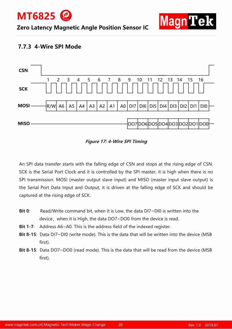
An SPI data transfer starts with the falling edge of CSN and stops at the rising edge of CSN.
SCK is the Serial Port Clock and it is controlled by the SPI master, it is high when there is no
SPI transmission. MOSI (master output slave input) and MISO (master input slave output) is
the Serial Port Data Input and Output, it is driven at the falling edge of SCK and should be
captured at the rising edge of SCK.
Bit 0: Read/Write command bit, when it is Low, the data DI7~DI0 is written into the
device,when it is High, the data DO7~DO0 from the device is read.
Bit 1-7: Address A6~A0. This is the address field of the indexed register.
Bit 8-15: Data DI7~DI0 (write mode). This is the data that will be written into the device (MSB
first).
Bit 8-15: Data DO7~DO0 (read mode). This is the data that will be read from the device (MSB
first).
Figure 17: 4-Wire SPI Timing
7.7.3 4-Wire SPI Mode
R/W A6 A5 A4 A3 A2 A1 A0 DI7 DI6 DI5 DI4 DI3 DI2 DI1 DI0
CSN
SCK
MOSI
MISO DO7 DO6 DO5 DO4 DO3 DO2 DO1 DO0
1 2 3 4 5 6 7 8 9 10 11 12 13 14 15 16

www.magntek.com.cn| Magnetic Tech Makes Magic Change Rev 1.0 2019.07
Zero Latency Magnetic Angle Position Sensor IC
MT6825
21
7.7.4 3-Wire SPI Mode
Figure 18: 3-Wire SPI Timing
An SPI data transfer starts with the falling edge of CSN and stops at the rising edge of CSN.
SCK is the Serial Port Clock and it is controlled by the SPI master, it is high when there is no SPI
transmission. SDAT is the Serial Port Data Input and Output, and it is driven at the falling edge
of SCK and should be captured at the rising edge of SCK.
Bit 0: Read/Write command bit. When it is Low, the data D7~D0 is written into the device.
When it is High, the data D7~D0 from the device is read.
Bit 1-7: address A6~A0. This is the address field of the indexed register.
Bit 8-15: data D7~D0 (write mode). This is the data that will be written into the device (MSB
first).
Bit 8-15: data D7~D0 (read mode). This is the data that will be read from the device (MSB
first).
R/W A6 A5 A4 A3 A2 A1 A0 D7 D6 D5 D4 D3 D2 D1 D0
CSN
SCK
SDAT
0 2 3 4 5 6 7 8 9 10 11 12 13 14 151

www.magntek.com.cn| Magnetic Tech Makes Magic Change Rev 1.0 2019.07
Zero Latency Magnetic Angle Position Sensor IC
MT6825
22
Figure 19: 4-Wire SPI Single Byte Read Angle Register
7.7.5 SPI Read Angle Register (e.g. 4-Wire SPI)
Reg. Address Bit7 Bit6 Bit5 Bit4 Bit3 Bit2 Bit1 Bit0
0x03 Angle<17:10>
0x04 Angle<9:4> No_Mag_Warning PC1
0x05 Angle<3:0> Over_Speed PC2 NA NA
Angle Data Register
0~360° absolute angle θ could be calculated by the below formula:17
0
2= 360
262144
i
i
Angle i
Bit 0x04[1] is a diagnosed bit for not enough magnet flux density. When the MT6825 could notdetect enough magnetic field for proper operation, this bit is set to high.
Bit 0x05[3] ] is a diagnosed bit, when MT6825 detects the rotation speed exceeding the upperlimitation, this bit is set to high.
Bit 0x04[0] is a parity check bit and it follows even check rule. If 0x03[7:0] and 0x04[7:1] totallyhave even number of logic high, 0x04[0]=0. If 0x03[7:0] and 0x04[7:1] totally have odd number oflogic high, 0x04[0]=1.
Bit 0x05[2] is a parity check bit and it follows even check rule. If 0x05[7:3] totally have evennumber of logic high, 0x05[2]=0. If 0x05[7:3] totally have odd number of logic high, 0x05[2]=1.
Read Reg. 0x03
Data of Reg. 0x03MISO
MOSI
CSN
SCK
Read Reg. 0x04
Data of Reg. 0x04
Read Reg. 0x05
Data of Reg. 0x05

www.magntek.com.cn| Magnetic Tech Makes Magic Change Rev 1.0 2019.07
Zero Latency Magnetic Angle Position Sensor IC
MT6825
23
Figure 20: 4-Wire SPI Burst Read Angle Registers
Figure 21: 3-Wire SPI Single Byte Read Angle Registers
The MT6825 provides an SPI burst read mode for faster data rate than single byte read mode
as shown in Figure 20.
Figure 22: 3-Wire SPI Burst Read Angle Registers
Read Reg. 0x03 Data Reg. 0x03SDAT
CSN
SCK
Read Reg. 0x04 Data Reg. 0x04
MCU Output MCU Output
Read Reg. 0x05 Data Reg. 0x05
MCU Output MT6825 Output
MT6825 Output
MT6825 Output
Read Reg. 0x03 Data Reg. 0x03SDAT
CSN
SCK
Data Reg. 0x04 Data Reg. 0x05 Data Reg. 0x03
Data N Data N+1
…
Read Reg. 0x03
Data of Reg. 0x03MISO
MOSI
CSN
SCK
Data of Reg. 0x04
Data of Reg. 0x05
Data of Reg. 0x03
Data of Reg. 0x04
Data of Reg. 0x05
Data N Data N+1
... ...
... ...

www.magntek.com.cn| Magnetic Tech Makes Magic Change Rev 1.0 2019.07
Zero Latency Magnetic Angle Position Sensor IC
MT6825
24
8. MTP Programming
24
MT6825 have a build in MTP memory for customer to program resolution, zero position, z-
pulse width and etc. parameters. MTP programming needs SPI communication and a 7V DC
supply for HVPP pin. If customer wants to know the detail programming method, please
contact MagnTek’s sales office for technical supporting.
Figure 23: MTP Programming
VDD
1 8
16 915 14 13 12 11 10
2 3 4 5 6 7
TVS(6V)
PWM
U V W
A B Z Erro
r
HVPP
1uf
MIS
O
MO
SI
SCK
CSN
0.1uf
VDD
HVPP MTP Programming
3.3~5.0V
0V
7V
0V
NormalOperation
NormalOperation

www.magntek.com.cn| Magnetic Tech Makes Magic Change Rev 1.0 2019.07
Zero Latency Magnetic Angle Position Sensor IC
MT6825
25
It is required that the magnet’s center axis be aligned with the sensing element center of
MT6825 with the air-gap as small as possible. Any misalignment introduces additional
angle error and big air-gap also weakens the magnet field which could be sensed by the
device. Magnets with larger diameter are more tolerant to DISP (off-axis misalignment)
and big AG (air-gap between Magnet and device).
9. Magnet Placement
0
0.1
0.2
0.3
0.4
0.5
0.6
0.7
0.8
0 0.1 0.2 0.3 0.4 0.5 0.6
INL(deg)
DISP (mm)
INL vs. DISP for Φ10 magnet
AG=1mm
AG=3mm
AG=5mm

www.magntek.com.cn| Magnetic Tech Makes Magic Change Rev 1.0 2019.07
1 8
16 915 14 13 12 11 10
2 3 4 5 6 7 1 8
16 915 14 13 12 11 10
2 3 4 5 6 7
1 8
16 915 14 13 12 11 10
2 3 4 5 6 7 1 8
16 915 14 13 12 11 10
2 3 4 5 6 7
0 degree 90 degree
180 degree 270 degree
S
N S N
SN
S
N
Zero Latency Magnetic Angle Position Sensor IC
MT6825
26
10. Mechanical Angle Direction

www.magntek.com.cn| Magnetic Tech Makes Magic Change Rev 1.0 2019.07
Y
X
Z
Zero Latency Magnetic Angle Position Sensor IC
MT6825
27
11. Package Information
27
SymbolDimensions in Millimeters Dimensions in Inches
Min. Max. Min. Max.D 4.900 5.100 0.193 0.201E 6.250 6.550 0.246 0.258b 0.190 0.300 0.007 0.012c 0.090 0.200 0.004 0.008
E1 4.300 4.500 0.169 0.177A 1.200 0.047
A2 0.800 1.000 0.031 0.039A1 0.050 0.150 0.002 0.006e 0.65 (BSC) 0.026 (BSC)L 0.500 0.700 0.020 0.028H 0.25 (TYP) 0.01 (TYP)θ 1° 7° 1° 7°X 2.450 2.550 0.097 0.101Y 2.150 2.250 0.085 0.089Z 0.210 0.370 0.016 0.024

www.magntek.com.cn| Magnetic Tech Makes Magic Change Rev 1.0 2019.07
Zero Latency Magnetic Angle Position Sensor IC
MT6825
28
12. Copy Rights and Disclaimer
28
1. This document may not be reproduced or duplicated, in any form, in whole or in part
without prior written consent of MagnTek . Copyrights © 2019, MagnTek Incorporated.
2. MagnTek reserves the right to make changes to the information published in this
document at anytime without notice.
3. MagnTek’s products are limited for use in normal commercial applications.
MagnTek’s products are not to be used in any device or system, including but not
limited to medical life support equipment and system.
For the latest version of this document, please visit our website: www.magntek.com.cn

www.magntek.com.cn| Magnetic Tech Makes Magic Change Rev 1.0 2019.07
Zero Latency Magnetic Angle Position Sensor IC
MT6825
29
13. Revision History
29
Revision Number Date Comments
1.0 2019.07.08 Initial Release
Recommended