Embed Size (px)
Citation preview
This is information on a product in full production.
March 2015 DocID13844 Rev 6 1/30
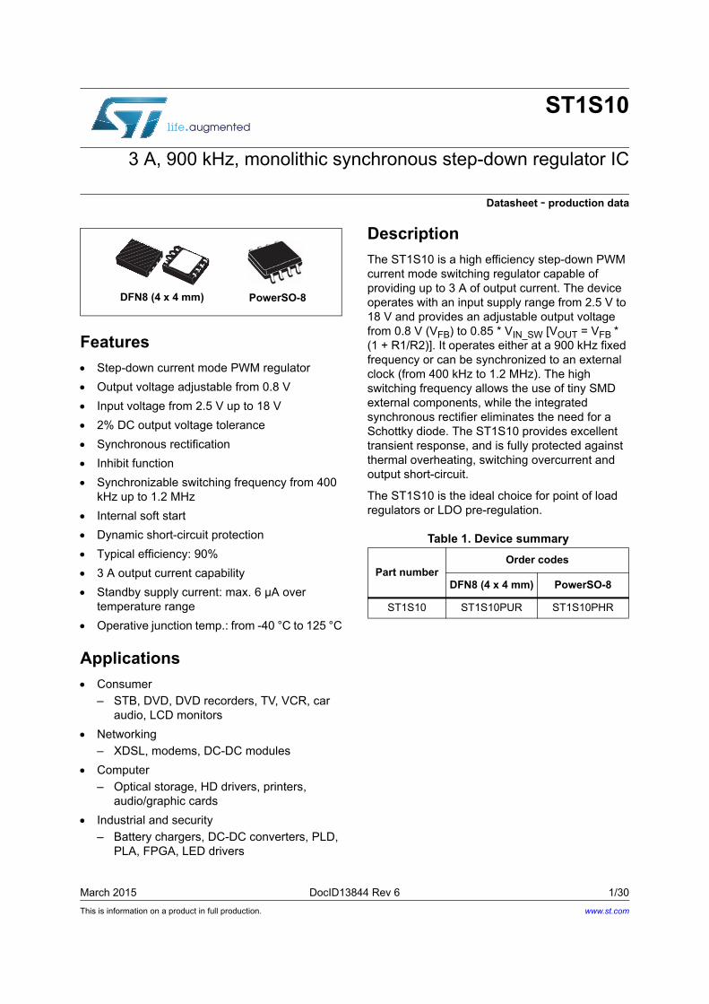
ST1S10
3 A, 900 kHz, monolithic synchronous step-down regulator IC
Datasheet - production data
Features
Step-down current mode PWM regulator
Output voltage adjustable from 0.8 V
Input voltage from 2.5 V up to 18 V
2% DC output voltage tolerance
Synchronous rectification
Inhibit function
Synchronizable switching frequency from 400 kHz up to 1.2 MHz
Internal soft start
Dynamic short-circuit protection
Typical efficiency: 90%
3 A output current capability
Standby supply current: max. 6 µA over temperature range
Operative junction temp.: from -40 °C to 125 °C
Applications
Consumer
– STB, DVD, DVD recorders, TV, VCR, car audio, LCD monitors
Networking
– XDSL, modems, DC-DC modules
Computer
– Optical storage, HD drivers, printers, audio/graphic cards
Industrial and security
– Battery chargers, DC-DC converters, PLD, PLA, FPGA, LED drivers
Description
The ST1S10 is a high efficiency step-down PWM current mode switching regulator capable of providing up to 3 A of output current. The device operates with an input supply range from 2.5 V to 18 V and provides an adjustable output voltage from 0.8 V (VFB) to 0.85 * VIN_SW [VOUT = VFB * (1 + R1/R2)]. It operates either at a 900 kHz fixed frequency or can be synchronized to an external clock (from 400 kHz to 1.2 MHz). The high switching frequency allows the use of tiny SMD external components, while the integrated synchronous rectifier eliminates the need for a Schottky diode. The ST1S10 provides excellent transient response, and is fully protected against thermal overheating, switching overcurrent and output short-circuit.
The ST1S10 is the ideal choice for point of load regulators or LDO pre-regulation.
PowerSO-8DFN8 (4 x 4 mm)
Table 1. Device summary
Part numberOrder codes
DFN8 (4 x 4 mm) PowerSO-8
ST1S10 ST1S10PUR ST1S10PHR
www.st.com
Contents ST1S10
2/30 DocID13844 Rev 6
Contents
1 Application circuit . . . . . . . . . . . . . . . . . . . . . . . . . . . . . . . . . . . . . . . . . . . 5
2 Pin configuration . . . . . . . . . . . . . . . . . . . . . . . . . . . . . . . . . . . . . . . . . . . . 6
3 Maximum ratings . . . . . . . . . . . . . . . . . . . . . . . . . . . . . . . . . . . . . . . . . . . . 7
4 Electrical characteristics . . . . . . . . . . . . . . . . . . . . . . . . . . . . . . . . . . . . . 8
5 Application information . . . . . . . . . . . . . . . . . . . . . . . . . . . . . . . . . . . . . 10
5.1 Description . . . . . . . . . . . . . . . . . . . . . . . . . . . . . . . . . . . . . . . . . . . . . . . . 10
5.2 External components selection . . . . . . . . . . . . . . . . . . . . . . . . . . . . . . . . 10
Input capacitor . . . . . . . . . . . . . . . . . . . . . . . . . . . . . . . . . . . . . . . . . . . . . . . . . . . . 10
5.3 Output capacitor (VOUT > 2.5 V) . . . . . . . . . . . . . . . . . . . . . . . . . . . . . . . . .11
5.4 Output capacitor (0.8 V < VOUT < 2.5 V) . . . . . . . . . . . . . . . . . . . . . . . . . 12
5.5 Output voltage selection . . . . . . . . . . . . . . . . . . . . . . . . . . . . . . . . . . . . . . 12
5.6 Inductor (VOUT > 2.5 V) . . . . . . . . . . . . . . . . . . . . . . . . . . . . . . . . . . . . . . 13
5.7 Inductor (0.8 V < VOUT < 2.5 V) . . . . . . . . . . . . . . . . . . . . . . . . . . . . . . . . 13
5.8 Function operation . . . . . . . . . . . . . . . . . . . . . . . . . . . . . . . . . . . . . . . . . . 13
5.8.1 Sync operation . . . . . . . . . . . . . . . . . . . . . . . . . . . . . . . . . . . . . . . . . . . . 13
5.8.2 Inhibit function . . . . . . . . . . . . . . . . . . . . . . . . . . . . . . . . . . . . . . . . . . . . 14
5.8.3 OCP (overcurrent protection) . . . . . . . . . . . . . . . . . . . . . . . . . . . . . . . . . 14
5.8.4 SCP (short-circuit protection) . . . . . . . . . . . . . . . . . . . . . . . . . . . . . . . . . 14
5.8.5 SCP and OCP operation with high capacitive load . . . . . . . . . . . . . . . . 14
6 Layout considerations . . . . . . . . . . . . . . . . . . . . . . . . . . . . . . . . . . . . . . 16
Thermal considerations. . . . . . . . . . . . . . . . . . . . . . . . . . . . . . . . . . . . . . . . . . . . . 17
7 Diagram . . . . . . . . . . . . . . . . . . . . . . . . . . . . . . . . . . . . . . . . . . . . . . . . . . 18
8 Typical performance characteristics . . . . . . . . . . . . . . . . . . . . . . . . . . . 19
DocID13844 Rev 6 3/30
ST1S10 Contents
30
9 Package information . . . . . . . . . . . . . . . . . . . . . . . . . . . . . . . . . . . . . . . . 22
9.1 Power SO-8 package information . . . . . . . . . . . . . . . . . . . . . . . . . . . . . . 22
9.2 DFN8 (4 x 4) package information . . . . . . . . . . . . . . . . . . . . . . . . . . . . . . 26
10 Revision history . . . . . . . . . . . . . . . . . . . . . . . . . . . . . . . . . . . . . . . . . . . 28
List of tables ST1S10
4/30 DocID13844 Rev 6
List of tables
Table 1. Device summary . . . . . . . . . . . . . . . . . . . . . . . . . . . . . . . . . . . . . . . . . . . . . . . . . . . . . . . . . . 1Table 2. Pin description . . . . . . . . . . . . . . . . . . . . . . . . . . . . . . . . . . . . . . . . . . . . . . . . . . . . . . . . . . . 7Table 3. Absolute maximum ratings . . . . . . . . . . . . . . . . . . . . . . . . . . . . . . . . . . . . . . . . . . . . . . . . . . 8Table 4. Thermal data. . . . . . . . . . . . . . . . . . . . . . . . . . . . . . . . . . . . . . . . . . . . . . . . . . . . . . . . . . . . . 8Table 5. ESD protection . . . . . . . . . . . . . . . . . . . . . . . . . . . . . . . . . . . . . . . . . . . . . . . . . . . . . . . . . . . 8Table 6. Electrical characteristics . . . . . . . . . . . . . . . . . . . . . . . . . . . . . . . . . . . . . . . . . . . . . . . . . . . . 9Table 7. Power SO-8 (exposed pad) package mechanical data . . . . . . . . . . . . . . . . . . . . . . . . . . . 24Table 8. Power SO-8 (exposed pad) tape and reel mechanical data . . . . . . . . . . . . . . . . . . . . . . . . 26Table 9. DFN8 (4 x 4) package mechanical data . . . . . . . . . . . . . . . . . . . . . . . . . . . . . . . . . . . . . . . 27Table 10. DFN8 (4 x 4) tape and reel mechanical data . . . . . . . . . . . . . . . . . . . . . . . . . . . . . . . . . . . 28Table 11. Document revision history . . . . . . . . . . . . . . . . . . . . . . . . . . . . . . . . . . . . . . . . . . . . . . . . . 29
DocID13844 Rev 6 5/30
ST1S10 List of figures
30
List of figures
Figure 1. Typical application circuit . . . . . . . . . . . . . . . . . . . . . . . . . . . . . . . . . . . . . . . . . . . . . . . . . . . 6Figure 2. Pin connections (top view for PowerSO-8, bottom view for DFN8) . . . . . . . . . . . . . . . . . . . 7Figure 3. Application schematic for heavy capacitive load . . . . . . . . . . . . . . . . . . . . . . . . . . . . . . . . 16Figure 4. Application schematic for low output voltage (VOUT < 2.5 V) and 2.5 V < VIN < 8 V . . . . . 16Figure 5. Application schematic for low output voltage (VOUT < 2.5 V) and 8 V < VIN < 16 V . . . . . . 16Figure 6. PCB layout suggestion - top . . . . . . . . . . . . . . . . . . . . . . . . . . . . . . . . . . . . . . . . . . . . . . . . 17Figure 7. PCB layout suggestion - bottom . . . . . . . . . . . . . . . . . . . . . . . . . . . . . . . . . . . . . . . . . . . . . 18Figure 8. Block diagram . . . . . . . . . . . . . . . . . . . . . . . . . . . . . . . . . . . . . . . . . . . . . . . . . . . . . . . . . . . 19Figure 9. Voltage feedback vs. temperature . . . . . . . . . . . . . . . . . . . . . . . . . . . . . . . . . . . . . . . . . . . 20Figure 10. Oscillator frequency vs. temperature . . . . . . . . . . . . . . . . . . . . . . . . . . . . . . . . . . . . . . . . . 20Figure 11. Max. duty cycle vs. temperature . . . . . . . . . . . . . . . . . . . . . . . . . . . . . . . . . . . . . . . . . . . . . 20Figure 12. Inhibit threshold vs. temperature . . . . . . . . . . . . . . . . . . . . . . . . . . . . . . . . . . . . . . . . . . . . 20Figure 13. Reference line regulation vs. temperature . . . . . . . . . . . . . . . . . . . . . . . . . . . . . . . . . . . . . 21Figure 14. Reference load regulation vs. temperature. . . . . . . . . . . . . . . . . . . . . . . . . . . . . . . . . . . . . 21Figure 15. ON mode quiescent current vs. temperature . . . . . . . . . . . . . . . . . . . . . . . . . . . . . . . . . . . 21Figure 16. Shutdown mode quiescent current vs. temperature . . . . . . . . . . . . . . . . . . . . . . . . . . . . . . 21Figure 17. PMOS ON resistance vs. temperature . . . . . . . . . . . . . . . . . . . . . . . . . . . . . . . . . . . . . . . . 21Figure 18. NMOS ON resistance vs. temperature . . . . . . . . . . . . . . . . . . . . . . . . . . . . . . . . . . . . . . . . 21Figure 19. Efficiency vs. temperature . . . . . . . . . . . . . . . . . . . . . . . . . . . . . . . . . . . . . . . . . . . . . . . . . 22Figure 20. Efficiency vs. output current at Vout = 5 V . . . . . . . . . . . . . . . . . . . . . . . . . . . . . . . . . . . . . . 22Figure 21. Efficiency vs. output current at Vout = 3.3 V . . . . . . . . . . . . . . . . . . . . . . . . . . . . . . . . . . . . 22Figure 22. Efficiency vs. output current at Vout = 12 V . . . . . . . . . . . . . . . . . . . . . . . . . . . . . . . . . . . . . 22Figure 23. Power SO-8 (exposed pad) package outline . . . . . . . . . . . . . . . . . . . . . . . . . . . . . . . . . . . 23Figure 24. Power SO-8 (exposed pad) recommended footprint . . . . . . . . . . . . . . . . . . . . . . . . . . . . . 25Figure 25. Power SO-8 (exposed pad) tape and reel dimensions . . . . . . . . . . . . . . . . . . . . . . . . . . . . 26Figure 26. DFN8 (4 x 4) package outline . . . . . . . . . . . . . . . . . . . . . . . . . . . . . . . . . . . . . . . . . . . . . . . 27Figure 27. DFN8 (4 x 4) tape and reel dimensions . . . . . . . . . . . . . . . . . . . . . . . . . . . . . . . . . . . . . . . 28
Application circuit ST1S10
6/30 DocID13844 Rev 6
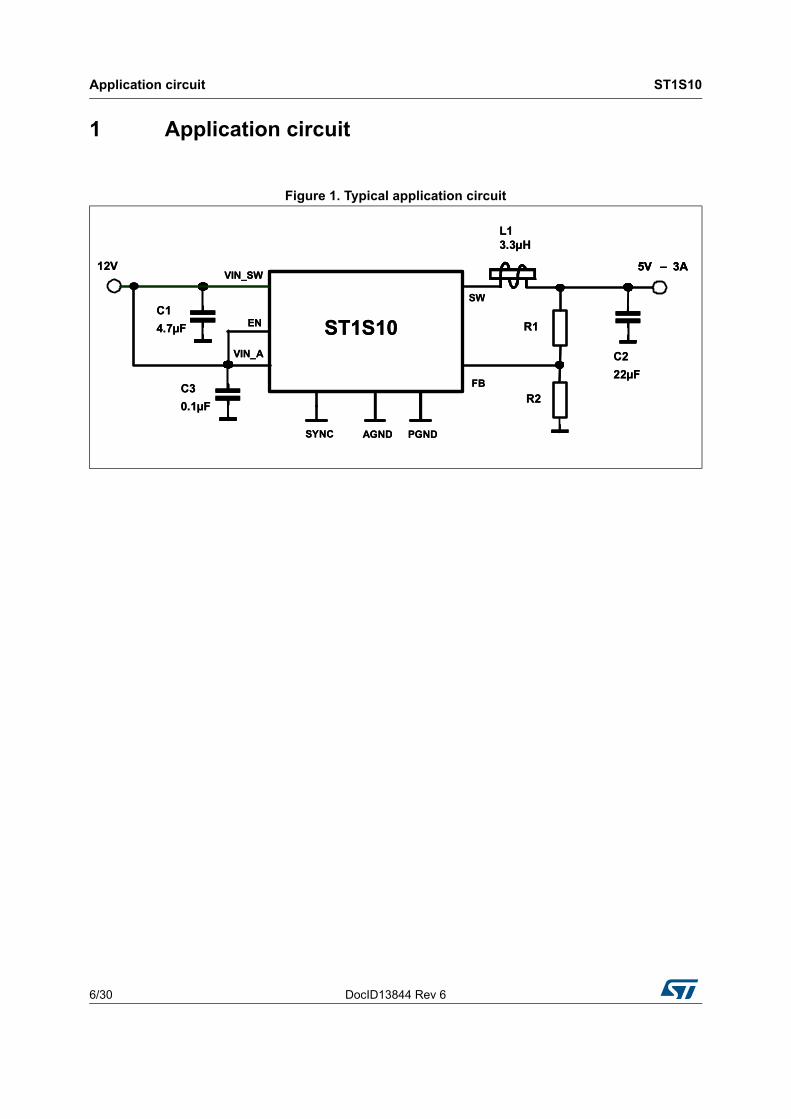
1 Application circuit
Figure 1. Typical application circuit
ST1S10
12V
L13.3µH
C1
4.7µF
SW
FB
C2
22µF
VIN_SW
SYNC
EN
5V – 3A
R1
R2
VIN_A
AGND PGND
C3
0.1µF
ST1S10
12V
L13.3µH
C1
4.7µF
SW
FB
C2
22µF
VIN_SW
SYNC
EN
5V – 3A5V – 3A
R1
R2
VIN_A
AGND PGND
C3
0.1µF
DocID13844 Rev 6 7/30
ST1S10 Pin configuration
30
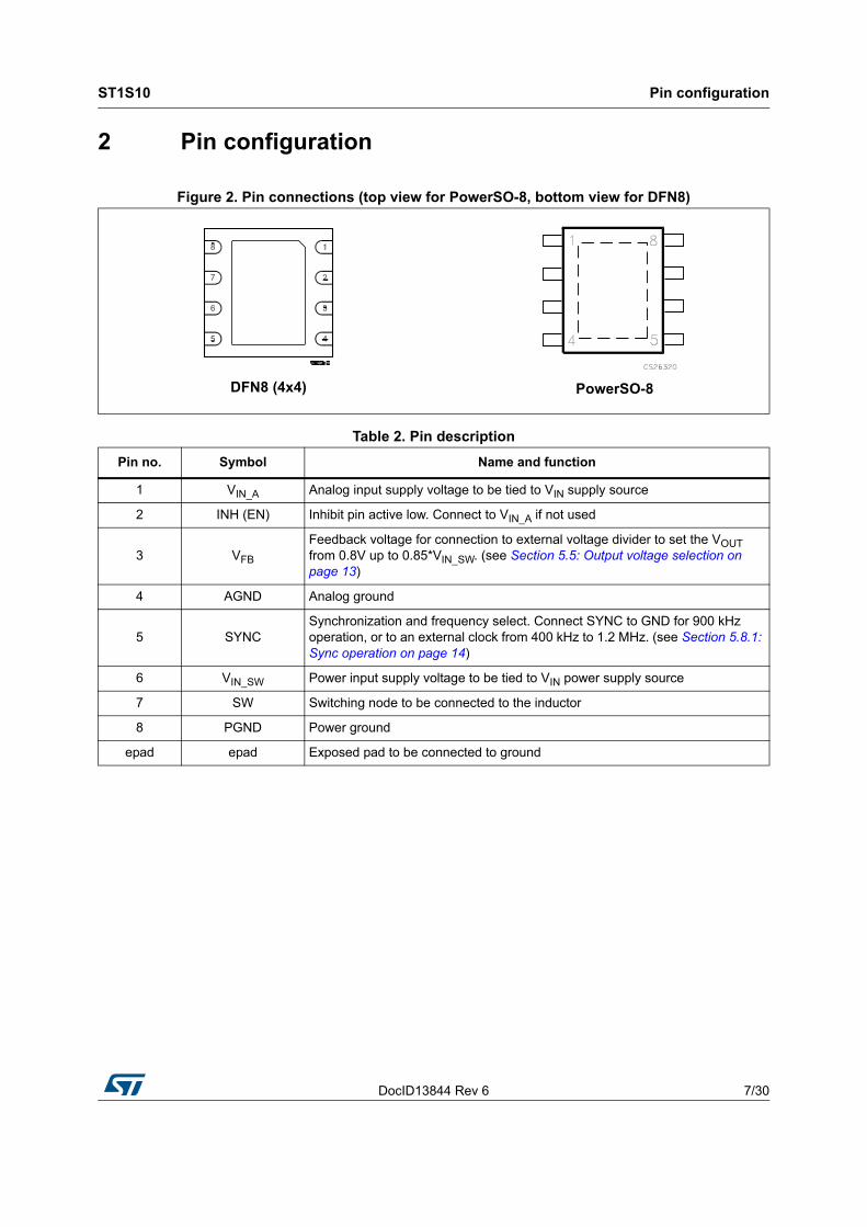
2 Pin configuration
Figure 2. Pin connections (top view for PowerSO-8, bottom view for DFN8)
PowerSO-8DFN8 (4x4)
Table 2. Pin description
Pin no. Symbol Name and function
1 VIN_A Analog input supply voltage to be tied to VIN supply source
2 INH (EN) Inhibit pin active low. Connect to VIN_A if not used
3 VFB
Feedback voltage for connection to external voltage divider to set the VOUT from 0.8V up to 0.85*VIN_SW. (see Section 5.5: Output voltage selection on page 13)
4 AGND Analog ground
5 SYNCSynchronization and frequency select. Connect SYNC to GND for 900 kHz operation, or to an external clock from 400 kHz to 1.2 MHz. (see Section 5.8.1: Sync operation on page 14)
6 VIN_SW Power input supply voltage to be tied to VIN power supply source
7 SW Switching node to be connected to the inductor
8 PGND Power ground
epad epad Exposed pad to be connected to ground
Maximum ratings ST1S10
8/30 DocID13844 Rev 6
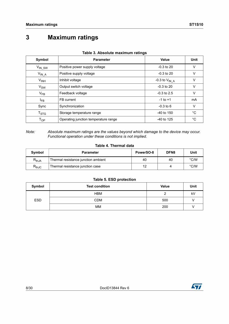
3 Maximum ratings
Note: Absolute maximum ratings are the values beyond which damage to the device may occur. Functional operation under these conditions is not implied.
Table 3. Absolute maximum ratings
Symbol Parameter Value Unit
VIN_SW Positive power supply voltage -0.3 to 20 V
VIN_A Positive supply voltage -0.3 to 20 V
VINH Inhibit voltage -0.3 to VIN_A V
VSW Output switch voltage -0.3 to 20 V
VFB Feedback voltage -0.3 to 2.5 V
IFB FB current -1 to +1 mA
Sync Synchronization -0.3 to 6 V
TSTG Storage temperature range -40 to 150 °C
TOP Operating junction temperature range -40 to 125 °C
Table 4. Thermal data
Symbol Parameter PowerSO-8 DFN8 Unit
RthJA Thermal resistance junction ambient 40 40 °C/W
RthJC Thermal resistance junction case 12 4 °C/W
Table 5. ESD protection
Symbol Test condition Value Unit
ESD
HBM 2 kV
CDM 500 V
MM 200 V
DocID13844 Rev 6 9/30
ST1S10 Electrical characteristics
30
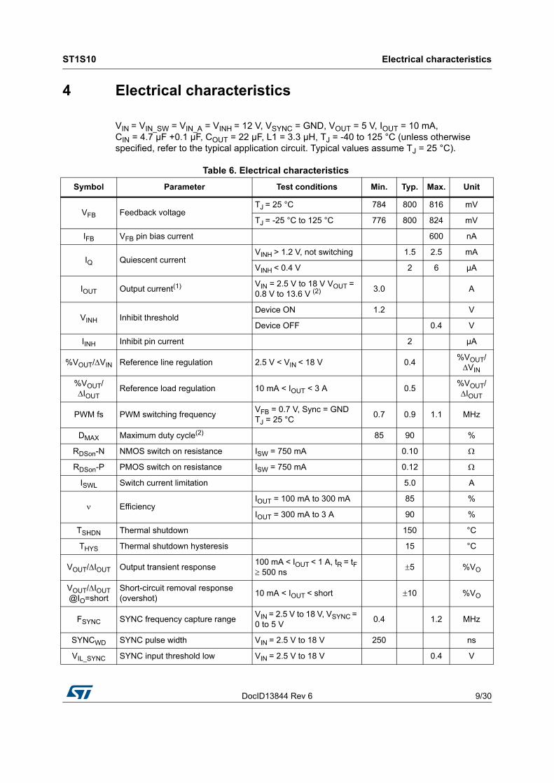
4 Electrical characteristics
VIN = VIN_SW = VIN_A = VINH = 12 V, VSYNC = GND, VOUT = 5 V, IOUT = 10 mA, CIN = 4.7 µF +0.1 µF, COUT = 22 µF, L1 = 3.3 µH, TJ = -40 to 125 °C (unless otherwise specified, refer to the typical application circuit. Typical values assume TJ = 25 °C).
Table 6. Electrical characteristics
Symbol Parameter Test conditions Min. Typ. Max. Unit
VFB Feedback voltageTJ = 25 °C 784 800 816 mV
TJ = -25 °C to 125 °C 776 800 824 mV
IFB VFB pin bias current 600 nA
IQ Quiescent currentVINH > 1.2 V, not switching 1.5 2.5 mA
VINH < 0.4 V 2 6 µA
IOUT Output current(1) VIN = 2.5 V to 18 V VOUT = 0.8 V to 13.6 V (2) 3.0 A
VINH Inhibit thresholdDevice ON 1.2 V
Device OFF 0.4 V
IINH Inhibit pin current 2 µA
%VOUT/VIN Reference line regulation 2.5 V < VIN < 18 V 0.4%VOUT/VIN
%VOUT/IOUT
Reference load regulation 10 mA < IOUT < 3 A 0.5%VOUT/IOUT
PWM fs PWM switching frequencyVFB = 0.7 V, Sync = GND TJ = 25 °C
0.7 0.9 1.1 MHz
DMAX Maximum duty cycle(2) 85 90 %
RDSon-N NMOS switch on resistance ISW = 750 mA 0.10
RDSon-P PMOS switch on resistance ISW = 750 mA 0.12
ISWL Switch current limitation 5.0 A
EfficiencyIOUT = 100 mA to 300 mA 85 %
IOUT = 300 mA to 3 A 90 %
TSHDN Thermal shutdown 150 °C
THYS Thermal shutdown hysteresis 15 °C
VOUT/IOUT Output transient response100 mA < IOUT < 1 A, tR = tF 500 ns
5 %VO
VOUT/IOUT @IO=short
Short-circuit removal response (overshot)
10 mA < IOUT < short 10 %VO
FSYNC SYNC frequency capture rangeVIN = 2.5 V to 18 V, VSYNC = 0 to 5 V
0.4 1.2 MHz
SYNCWD SYNC pulse width VIN = 2.5 V to 18 V 250 ns
VIL_SYNC SYNC input threshold low VIN = 2.5 V to 18 V 0.4 V
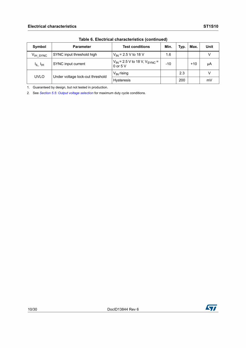
Electrical characteristics ST1S10
10/30 DocID13844 Rev 6
VIH_SYNC SYNC input threshold high VIN = 2.5 V to 18 V 1.6 V
IIL, IIH SYNC input currentVIN = 2.5 V to 18 V, VSYNC = 0 or 5 V
-10 +10 µA
UVLO Under voltage lock-out thresholdVIN rising 2.3 V
Hysteresis 200 mV
1. Guaranteed by design, but not tested in production.
2. See Section 5.5: Output voltage selection for maximum duty cycle conditions.
Table 6. Electrical characteristics (continued)
Symbol Parameter Test conditions Min. Typ. Max. Unit
DocID13844 Rev 6 11/30
ST1S10 Application information
30
5 Application information
5.1 Description
The ST1S10 is a high efficiency synchronous step-down DC-DC converter with inhibit function. It provides up to 3 A over an input voltage range of 2.5 V to 18 V, and the output voltage can be adjusted from 0.8 V up to 85% of the input voltage level. The synchronous rectification removes the need for an external Schottky diode and allows higher efficiency even at very low output voltages.
A high internal switching frequency (0.9 MHz) allows the use of tiny surface-mount components, as well as a resistor divider to set the output voltage value. In typical application conditions, only an inductor and 3 capacitors are required for proper operation.
The device can operate in PWM mode with a fixed frequency or synchronized to an external frequency through the SYNC pin. The current mode PWM architecture and stable operation with low ESR SMD ceramic capacitors results in low, predictable output ripple. No external compensation is needed.
To maximize power conversion efficiency, the ST1S10 works in pulse skipping mode at light load conditions and automatically switches to PWM mode when the output current increases.
The ST1S10 is equipped with thermal shutdown protection activated at 150 °C (typ.).
Cycle-by-cycle short-circuit protection provides protection against shorted outputs for the application and the regulator. An internal soft start for start-up current limiting and power ON delay of 275 µs (typ.) helps to reduce inrush current during start-up.
5.2 External components selection
Input capacitor
The ST1S10 features two VIN pins: VIN_SW for the power supply input voltage where the switching peak current is drawn, and VIN_A to supply the ST1S10 internal circuitry and drivers.
The VIN_SW input capacitor reduces the current peaks drawn from the input power supply and reduces switching noise in the IC. A high power supply source impedance requires larger input capacitance.
For the VIN_SW input capacitor the RMS current rating is a critical parameter that must be higher than the RMS input current. The maximum RMS input current can be calculated using the following equation:
Equation 1
where is the expected system efficiency, D is the duty cycle and IO is the output DC current. The duty cycle can be derived using Equation 2.
ηD
ηD2
-DII22
ORMS=
ηD
ηD2
-DII22
ORMS=
Application information ST1S10
12/30 DocID13844 Rev 6
Equation 2
D = (VOUT + VF) / (VIN-VSW)
where VF is the voltage drop across the internal NMOS, and VSW represents the voltage drop across the internal PDMOS. The minimum duty cycle (at VIN_max) and the maximum duty cycle (at VIN_min) should be considered in order to determine the max IRMS flowing through the input capacitor.
A minimum value of 4.7 µF for the VIN_SW and a 0.1 µF ceramic capacitor for the VIN_A are suitable in most application conditions. A 10 µF or higher ceramic capacitor for the VIN_SW and a 1 µF or higher for the VIN_A are recommended in cases of higher power supply source impedance or where long wires are needed between the power supply source and the VIN pins. The above higher input capacitor values are also recommended in cases where an output capacitive load is present (47 µF < CLOAD < 100 µF), which could impact the switching peak current drawn from the input capacitor during the start-up transient.
In cases of very high output capacitive loads (CLOAD > 100 µF), all input/output capacitor values shall be modified as described in Section 5.8.5: SCP and OCP operation with high capacitive load.
The input ceramic capacitors should have a voltage rating in the range of 1.5 times the maximum input voltage and be located as close as possible to VIN pins.
5.3 Output capacitor (VOUT > 2.5 V)
The most important parameters for the output capacitor are the capacitance, the ESR and the voltage rating. The capacitance and the ESR affect the control loop stability, the output ripple voltage and transient response of the regulator.
The ripple due to the capacitance can be calculated with the following equation:
Equation 3
VRIPPLE(C) = (0.125 x ISW) / (FS x COUT)
where FS is the PWM switching frequency and ISW is the inductor peak-to-peak switching current, which can be calculated as:
Equation 4
ISW = [(VIN - VOUT) / (FS x L)] x D
where D is the duty cycle.
The ripple due to the ESR is given by:
Equation 5
VRIPPLE(ESR) = ISW x ESR
The equations above can be used to define the capacitor selection range, but final values should be verified by testing an evaluation circuit.
Lower ESR ceramic capacitors are usually recommended to reduce the output ripple voltage. Capacitors with higher voltage ratings have lower ESR values, resulting in lower output ripple voltage.
DocID13844 Rev 6 13/30
ST1S10 Application information
30
Also, the capacitor ESL value impacts the output ripple voltage, but ceramic capacitors usually have very low ESL, making ripple voltages due to the ESL negligible. In order to reduce ripple voltages due to the parasitic inductive effect, the output capacitor connection paths should be kept as short as possible.
The ST1S10 has been designed to perform best with ceramic capacitors. Under typical application conditions a minimum ceramic capacitor value of 22 µF is recommended on the output, but higher values are suitable considering that the control loop has been designed to work properly with a natural output LC frequency provided by a 3.3 µH inductor and 22 µF output capacitor. If the high capacitive load application circuit shown in Figure 3 is used, a 47 µF (or 2 x 22 µF capacitors in parallel) could be needed as described in Section 5.8.5: SCP and OCP operation with high capacitive load.
The use of ceramic capacitors with voltage ratings in the range of 1.5 times the maximum output voltage is recommended.
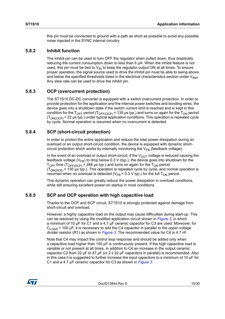
5.4 Output capacitor (0.8 V < VOUT < 2.5 V)
For applications with lower output voltage levels (Vout < 2.5 V) the output capacitance and inductor values should be selected in a way that improves the DC-DC control loop behavior. In this output condition two cases must be considered: VIN > 8 V and VIN < 8 V.
For VIN < 8 V the use of 2 x 22 µF capacitors in parallel to the output is recommended, as shown in Figure 4.
For VIN > 8 V, a 100 µF electrolytic capacitor with ESR < 0.1 should be added in parallel to the 2 x 22 µF output capacitors as shown in Figure 5.
5.5 Output voltage selection
The output voltage can be adjusted from 0.8 V up to 85% of the input voltage level by connecting a resistor divider (see R1 and R2 in the typical application circuit) between the output and the VFB pin. A resistor divider with R2 in the range of 20 k is a suitable compromise in terms of current consumption. Once the R2 value is selected, R1 can be calculated using the following equation:
Equation 6
R1 = R2 x (VOUT - VFB) / VFB
where VFB = 0.8 V (typ.).
Lower values are suitable as well, but will increase current consumption. Be aware that duty cycle must be kept below 85% at all application conditions, so that:
Equation 7
D = (VOUT + VF) / (VIN-VSW) < 0.85
where VF is the voltage drop across the internal NMOS, and VSW represents the voltage drop across the internal PDMOS.
Note that once the output current is fixed, higher VOUT levels increase the power dissipation of the device leading to an increase in the operating junction temperature. It is recommended to select a VOUT level which maintains the junction temperature below the
Application information ST1S10
14/30 DocID13844 Rev 6
thermal shut-down protection threshold (150°C typ.) at the rated output current. The following equation can be used to calculate the junction temperature (TJ):
Equation 8
TJ = {[VOUT x IOUT x RthJA x (1-)] / +TAMB
where RthJA is the junction to ambient thermal resistance, is the efficiency at the rated IOUT current and TAMB is the ambient temperature.
To ensure safe operating conditions the application should be designed to keep TJ < 140°C.
5.6 Inductor (VOUT > 2.5 V)
The inductor value fixes the ripple current flowing through output capacitor and switching peak current. The ripple current should be kept in the range of 20-40% of IOUT_MAX (for example it is 0.6 - 1.2 A at IOUT = 3 A). The approximate inductor value can be obtained with the following equation:
Equation 9
L = [(VIN - VOUT) / ISW] x TON
where TON is the ON time of the internal switch, given by:
TON = D/FS
The inductor should be selected with saturation current (ISAT) equal to or higher than the inductor peak current, which can be calculated with the following equation:
Equation 10
IPK = IO + (ISW/2), ISAT IPK
The inductor peak current must be designed so that it does not exceed the switching current limit.
5.7 Inductor (0.8 V < VOUT < 2.5 V)
For applications with lower output voltage levels (Vout < 2.5 V) the description in the previous section is still valid but it is recommended to keep the inductor values in a range from 1µH to 2.2 µH in order to improve the DC-DC control loop behavior, and increase the output capacitance depending on the VIN level as shown in Figure 4 and Figure 5. In most application conditions a 2.2 µH inductor is the best compromise between DC-DC control loop behavior and output voltage ripple.
5.8 Function operation
5.8.1 Sync operation
The ST1S10 operates at a fixed frequency or can be synchronized to an external frequency with the SYNC pin. The ST1S10 switches at a frequency of 900 kHz when the SYNC pin is connected to ground, and can synchronize the switching frequency between 400 kHz to 1.2 MHz from an external clock applied to the SYNC pin. When the SYNC feature is not used,
DocID13844 Rev 6 15/30
ST1S10 Application information
30
this pin must be connected to ground with a path as short as possible to avoid any possible noise injected in the SYNC internal circuitry.
5.8.2 Inhibit function
The inhibit pin can be used to turn OFF the regulator when pulled down, thus drastically reducing the current consumption down to less than 6 µA. When the inhibit feature is not used, this pin must be tied to VIN to keep the regulator output ON at all times. To ensure proper operation, the signal source used to drive the inhibit pin must be able to swing above and below the specified thresholds listed in the electrical characteristics section under VINH. Any slew rate can be used to drive the inhibit pin.
5.8.3 OCP (overcurrent protection)
The ST1S10 DC-DC converter is equipped with a switch overcurrent protection. In order to provide protection for the application and the internal power switches and bonding wires, the device goes into a shutdown state if the switch current limit is reached and is kept in this condition for the TOFF period (TOFF(OCP) = 135 µs typ.) and turns on again for the TON period (TON(OCP) = 22 µs typ.) under typical application conditions. This operation is repeated cycle by cycle. Normal operation is resumed when no overcurrent is detected.
5.8.4 SCP (short-circuit protection)
In order to protect the entire application and reduce the total power dissipation during an overload or an output short-circuit condition, the device is equipped with dynamic short-circuit protection which works by internally monitoring the VFB (feedback voltage).
In the event of an overload or output short-circuit, if the VOUT voltage is reduced causing the feedback voltage (VFB) to drop below 0.3 V (typ.), the device goes into shutdown for the TOFF time (TOFF(SCP) = 288 µs typ.) and turns on again for the TON period (TON(SCP) = 130 µs typ.). This operation is repeated cycle by cycle, and normal operation is resumed when no overload is detected (VFB > 0.3 V typ.) for the full TON period.
This dynamic operation can greatly reduce the power dissipation in overload conditions, while still ensuring excellent power-on startup in most conditions.
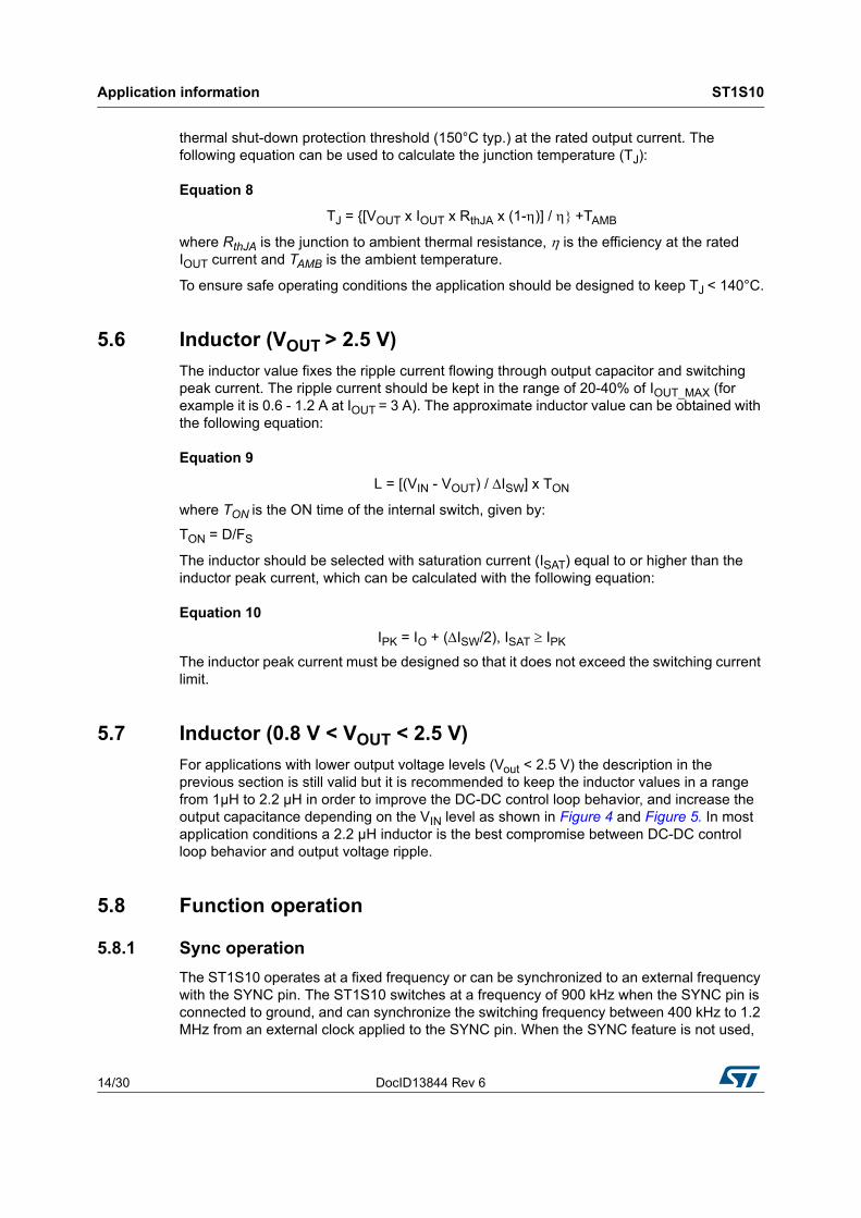
5.8.5 SCP and OCP operation with high capacitive load
Thanks to the OCP and SCP circuit, ST1S10 is strongly protected against damage from short-circuit and overload.
However, a highly capacitive load on the output may cause difficulties during start-up. This can be resolved by using the modified application circuit shown in Figure 3, in which a minimum of 10 µF for C1 and a 4.7 µF ceramic capacitor for C3 are used. Moreover, for CLOAD > 100 µF, it is necessary to add the C4 capacitor in parallel to the upper voltage divider resistor (R1) as shown in Figure 3. The recommended value for C4 is 4.7 nF.
Note that C4 may impact the control loop response and should be added only when a capacitive load higher than 100 µF is continuously present. If the high capacitive load is variable or not present at all times, in addition to C4 an increase in the output ceramic capacitor C2 from 22 µF to 47 µF (or 2 x 22 µF capacitors in parallel) is recommended. Also in this case it is suggested to further increase the input capacitors to a minimum of 10 µF for C1 and a 4.7 µF ceramic capacitor for C3 as shown in Figure 3.
Application information ST1S10
16/30 DocID13844 Rev 6
(*) see OCP and SCP descriptions for C2 and C4 selection.
Figure 3. Application schematic for heavy capacitive load
ST1S10
12V
L13.3µH
C1
10µF
SW
FB
VIN_SW
SYNC
EN R1
R2
VIN_A
AGND PGND
C3
4.7µF
C2(*)
22µF
5V – 3AC4 (*)
4.7nF
CLOAD
LOAD
Output Load
ST1S10
12V
L13.3µH
C1
10µF
SW
FB
VIN_SW
SYNC
EN R1
R2
VIN_A
AGND PGND
C3
4.7µF
C2(*)
22µF
5V – 3A5V – 3AC4 (*)
4.7nF
CLOADCLOAD
LOAD
Output Load
Figure 4. Application schematic for low output voltage (VOUT < 2.5 V) and 2.5 V < VIN < 8 V
ST1S10
VIN<8V
L12.2µH
C1
10µF
SW
FB
VIN_SW
SYNC
EN R1
R2
VIN_A
AGND PGND
C3
0.1µF
C2
2x22µF
0.8V<VOUT<2.5V
ST1S10
VIN<8V
L12.2µH
C1
10µF
SW
FB
VIN_SW
SYNC
EN R1
R2
VIN_A
AGND PGND
C3
0.1µF
C2
2x22µF
0.8V<VOUT<2.5V
Figure 5. Application schematic for low output voltage (VOUT < 2.5 V) and 8 V < VIN < 16 V
ST1S10
8V<VIN<16V
L12.2µH
C1
10µF
SW
FB
VIN_SW
SYNC
EN R1
R2
VIN_A
AGND PGND
C3
4.7µF
C2
2x22µF
0.8V<VOUT<2.5V
+
C5100µF ElectrolyticESR<0.1Ohm
ST1S10
8V<VIN<16V
L12.2µH
C1
10µF
SW
FB
VIN_SW
SYNC
EN R1
R2
VIN_A
AGND PGND
C3
4.7µF
C2
2x22µF
0.8V<VOUT<2.5V
+
C5100µF ElectrolyticESR<0.1Ohm
DocID13844 Rev 6 17/30
ST1S10 Layout considerations
30
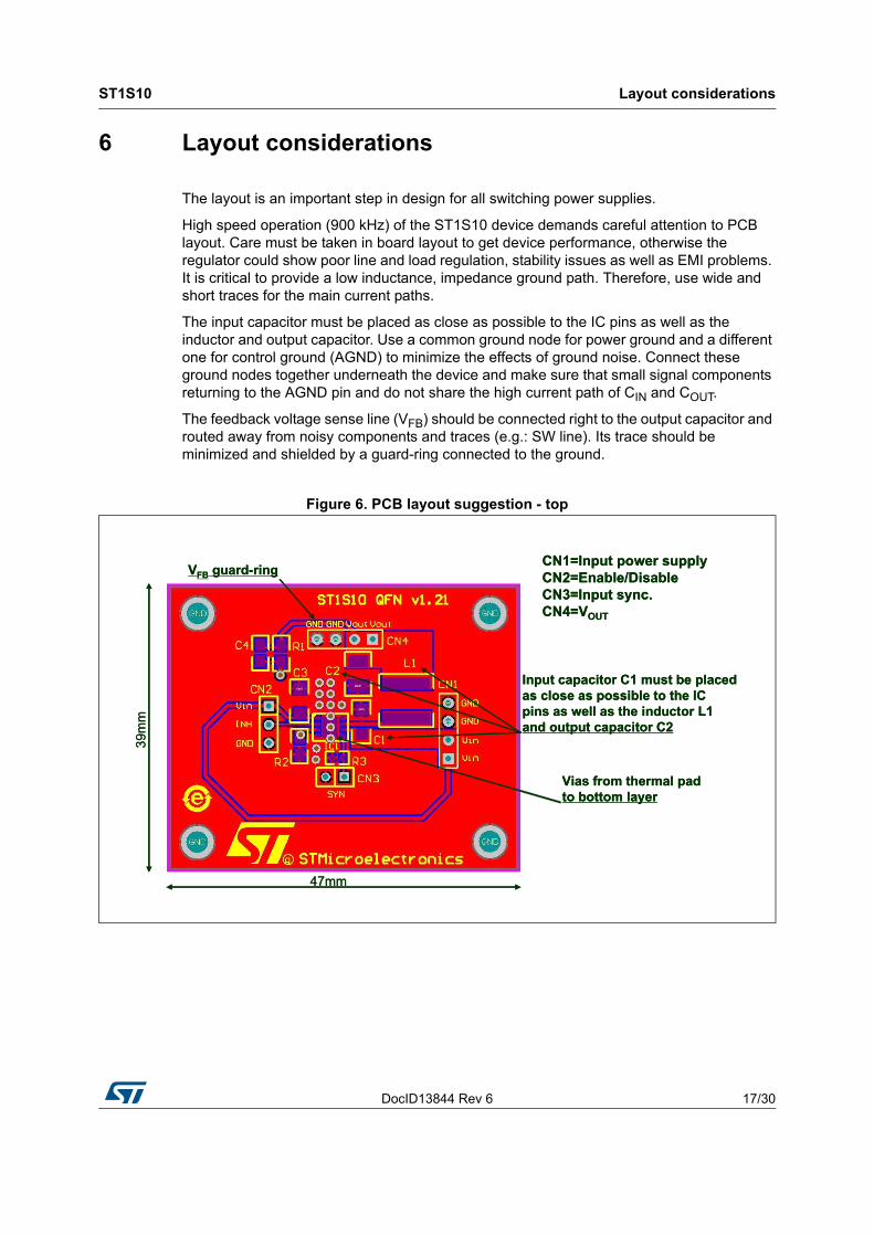
6 Layout considerations
The layout is an important step in design for all switching power supplies.
High speed operation (900 kHz) of the ST1S10 device demands careful attention to PCB layout. Care must be taken in board layout to get device performance, otherwise the regulator could show poor line and load regulation, stability issues as well as EMI problems. It is critical to provide a low inductance, impedance ground path. Therefore, use wide and short traces for the main current paths.
The input capacitor must be placed as close as possible to the IC pins as well as the inductor and output capacitor. Use a common ground node for power ground and a different one for control ground (AGND) to minimize the effects of ground noise. Connect these ground nodes together underneath the device and make sure that small signal components returning to the AGND pin and do not share the high current path of CIN and COUT.
The feedback voltage sense line (VFB) should be connected right to the output capacitor and routed away from noisy components and traces (e.g.: SW line). Its trace should be minimized and shielded by a guard-ring connected to the ground.
Figure 6. PCB layout suggestion - top
VFB guard-ring
Input capacitor C1 must be placedas close as possible to the ICpins as well as the inductor L1and output capacitor C2
Vias from thermal padto bottom layer
39m
m
47mm
CN1=Input power supplyCN2=Enable/DisableCN3=Input sync.CN4=VOUT
VFB guard-ring
Input capacitor C1 must be placedas close as possible to the ICpins as well as the inductor L1and output capacitor C2
Vias from thermal padto bottom layer
39m
m
47mm
CN1=Input power supplyCN2=Enable/DisableCN3=Input sync.CN4=VOUT
Layout considerations ST1S10
18/30 DocID13844 Rev 6
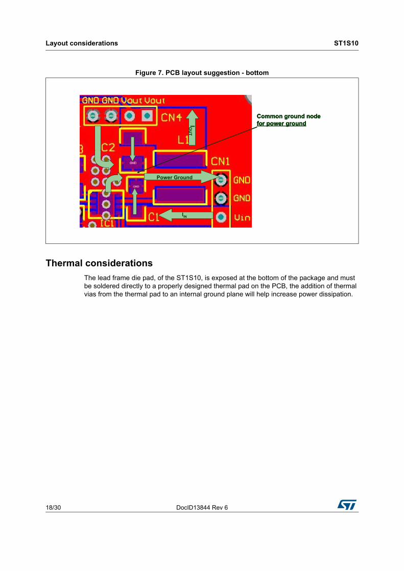
Thermal considerations
The lead frame die pad, of the ST1S10, is exposed at the bottom of the package and must be soldered directly to a properly designed thermal pad on the PCB, the addition of thermal vias from the thermal pad to an internal ground plane will help increase power dissipation.
Figure 7. PCB layout suggestion - bottom
Common ground nodefor power ground
IINIO
UT
Power Ground
Common ground nodefor power groundCommon ground nodefor power ground
IINIO
UT
Power Ground
DocID13844 Rev 6 19/30
ST1S10 Diagram
30
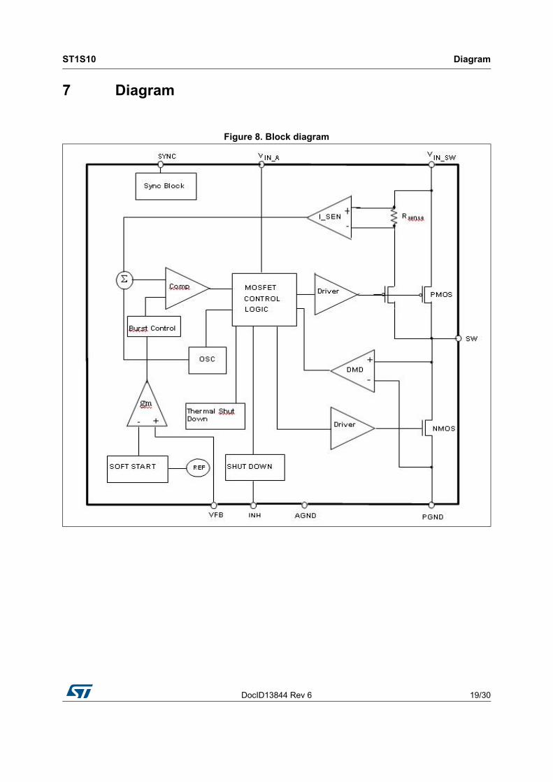
7 Diagram
Figure 8. Block diagram
Typical performance characteristics ST1S10
20/30 DocID13844 Rev 6
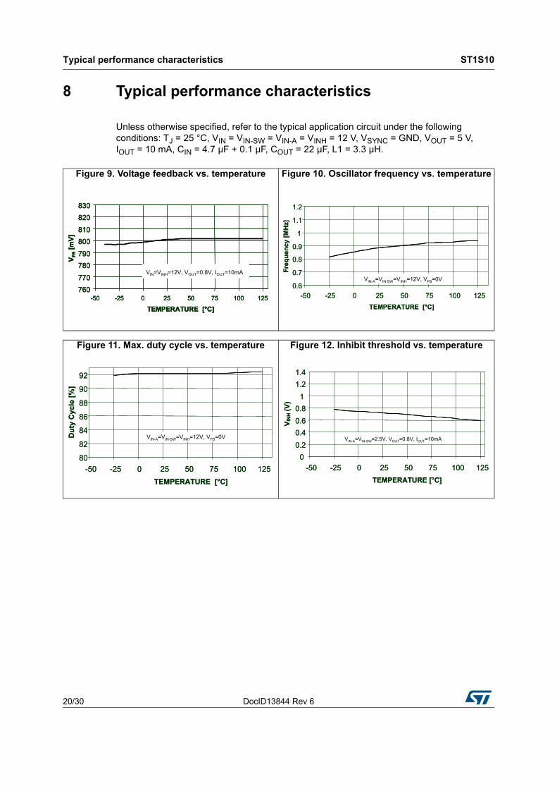
8 Typical performance characteristics
Unless otherwise specified, refer to the typical application circuit under the following conditions: TJ = 25 °C, VIN = VIN-SW = VIN-A = VINH = 12 V, VSYNC = GND, VOUT = 5 V,IOUT = 10 mA, CIN = 4.7 µF + 0.1 µF, COUT = 22 µF, L1 = 3.3 µH.
Figure 9. Voltage feedback vs. temperature Figure 10. Oscillator frequency vs. temperature
Figure 11. Max. duty cycle vs. temperature Figure 12. Inhibit threshold vs. temperature
760
770
780
790
800
810
820
830
-50 -25 0 25 50 75 100 125
TEMPERATURE [°C]
VF
B[m
V]
VIN=VINH=12V, VOUT=0.8V, IOUT=10mA
760
770
780
790
800
810
820
830
-50 -25 0 25 50 75 100 125
TEMPERATURE [°C]
VF
B[m
V]
760
770
780
790
800
810
820
830
-50 -25 0 25 50 75 100 125
TEMPERATURE [°C]
VF
B[m
V]
VIN=VINH=12V, VOUT=0.8V, IOUT=10mA
0.6
0.7
0.8
0.9
1
1.1
1.2
-50 -25 0 25 50 75 100 125
TEMPERATURE [°C]
Fre
qu
en
cy
[MH
z]VIN-A=VIN-SW=VINH=12V, VFB=0V
0.6
0.7
0.8
0.9
1
1.1
1.2
-50 -25 0 25 50 75 100 125
TEMPERATURE [°C]
Fre
qu
en
cy
[MH
z]VIN-A=VIN-SW=VINH=12V, VFB=0V
80
82
84
86
88
90
92
-50 -25 0 25 50 75 100 125
TEMPERATURE [°C]
Du
ty C
ycle
[%
]
VIN-A=VIN-SW=VINH=12V, VFB=0V
80
82
84
86
88
90
92
-50 -25 0 25 50 75 100 125
TEMPERATURE [°C]
Du
ty C
ycle
[%
]
VIN-A=VIN-SW=VINH=12V, VFB=0V
0
0.2
0.4
0.6
0.8
1
1.2
1.4
-50 -25 0 25 50 75 100 125
TEMPERATURE [°C]
VIN
H(V
)
VIN-A=VIN-SW=2.5V, VOUT=0.8V, IOUT=10mA
0
0.2
0.4
0.6
0.8
1
1.2
1.4
-50 -25 0 25 50 75 100 125
TEMPERATURE [°C]
VIN
H(V
)
VIN-A=VIN-SW=2.5V, VOUT=0.8V, IOUT=10mA
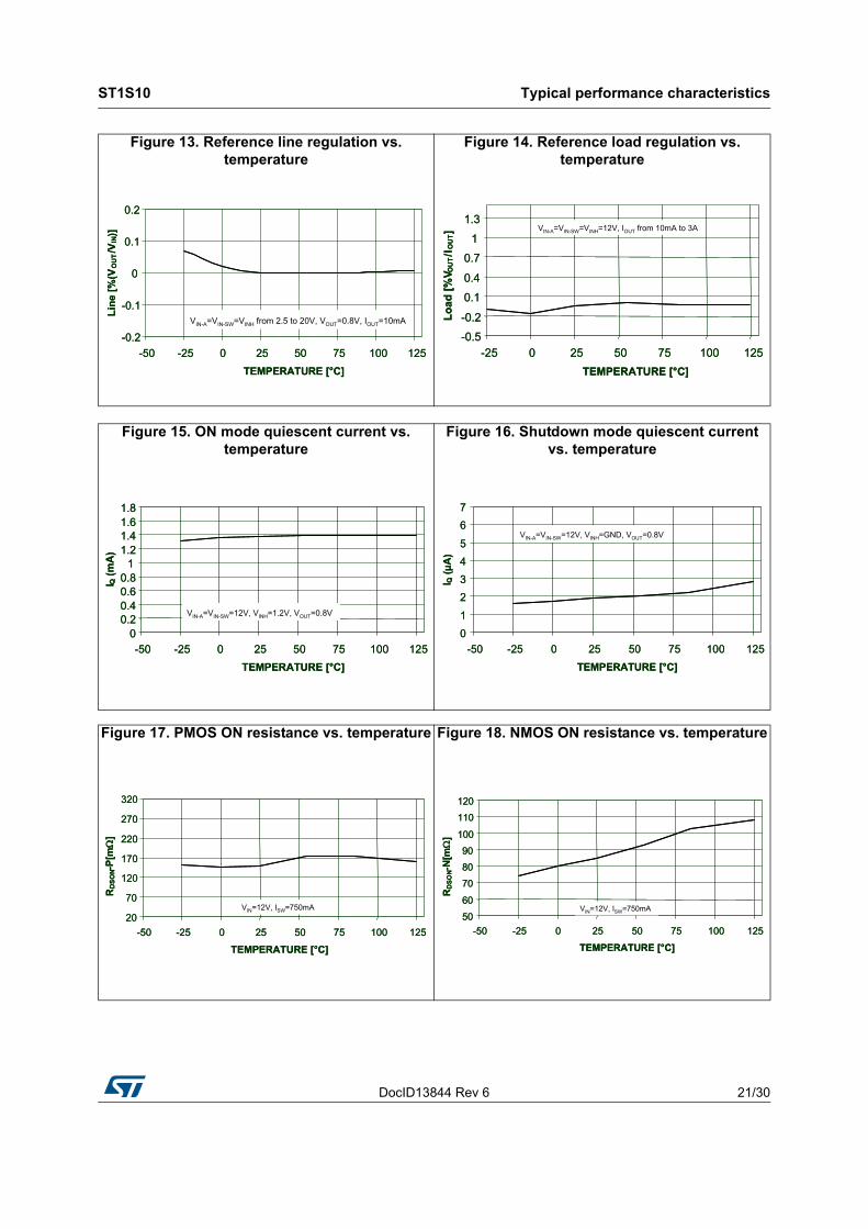
DocID13844 Rev 6 21/30
ST1S10 Typical performance characteristics
30
Figure 13. Reference line regulation vs. temperature
Figure 14. Reference load regulation vs. temperature
-0.2
-0.1
0
0.1
0.2
-50 -25 0 25 50 75 100 125
TEMPERATURE [°C]
Lin
e [%
(VO
UT/V
IN)]
VIN-A=VIN-SW=VINH from 2.5 to 20V, VOUT=0.8V, IOUT=10mA
-0.2
-0.1
0
0.1
0.2
-50 -25 0 25 50 75 100 125
TEMPERATURE [°C]
Lin
e [%
(VO
UT/V
IN)]
VIN-A=VIN-SW=VINH from 2.5 to 20V, VOUT=0.8V, IOUT=10mA
-0.5
-0.2
0.1
0.4
0.7
1
1.3
-25 0 25 50 75 100 125
TEMPERATURE [°C]
Lo
ad
[%
V OU
T/I
OU
T] VIN-A=VIN-SW=VINH=12V, IOUT from 10mA to 3A
-0.5
-0.2
0.1
0.4
0.7
1
1.3
-25 0 25 50 75 100 125
TEMPERATURE [°C]
Lo
ad
[%
V OU
T/I
OU
T] VIN-A=VIN-SW=VINH=12V, IOUT from 10mA to 3A
Figure 15. ON mode quiescent current vs. temperature
Figure 16. Shutdown mode quiescent current vs. temperature
Figure 17. PMOS ON resistance vs. temperature Figure 18. NMOS ON resistance vs. temperature
00.20.40.60.8
11.21.41.61.8
-50 -25 0 25 50 75 100 125
TEMPERATURE [°C]
I Q(m
A)
VIN-A=VIN-SW=12V, VINH=1.2V, VOUT=0.8V
00.20.40.60.8
11.21.41.61.8
-50 -25 0 25 50 75 100 125
TEMPERATURE [°C]
I Q(m
A)
VIN-A=VIN-SW=12V, VINH=1.2V, VOUT=0.8V
0
1
2
3
4
5
6
7
-50 -25 0 25 50 75 100 125
TEMPERATURE [°C]
I Q(µ
A)
VIN-A=VIN-SW=12V, VINH=GND, VOUT=0.8V
0
1
2
3
4
5
6
7
-50 -25 0 25 50 75 100 125
TEMPERATURE [°C]
I Q(µ
A)
VIN-A=VIN-SW=12V, VINH=GND, VOUT=0.8V
20
70
120
170
220
270
320
-50 -25 0 25 50 75 100 125
TEMPERATURE [°C]
RD
SO
N-P
[m
]
VIN=12V, ISW=750mA
20
70
120
170
220
270
320
-50 -25 0 25 50 75 100 125
TEMPERATURE [°C]
RD
SO
N-P
[m
]
VIN=12V, ISW=750mA50
60
70
80
90
100
110
120
-50 -25 0 25 50 75 100 125
TEMPERATURE [°C]
RD
SO
N-N
[m
]
VIN=12V, ISW=750mA50
60
70
80
90
100
110
120
-50 -25 0 25 50 75 100 125
TEMPERATURE [°C]
RD
SO
N-N
[m
]
VIN=12V, ISW=750mA
Typical performance characteristics ST1S10
22/30 DocID13844 Rev 6
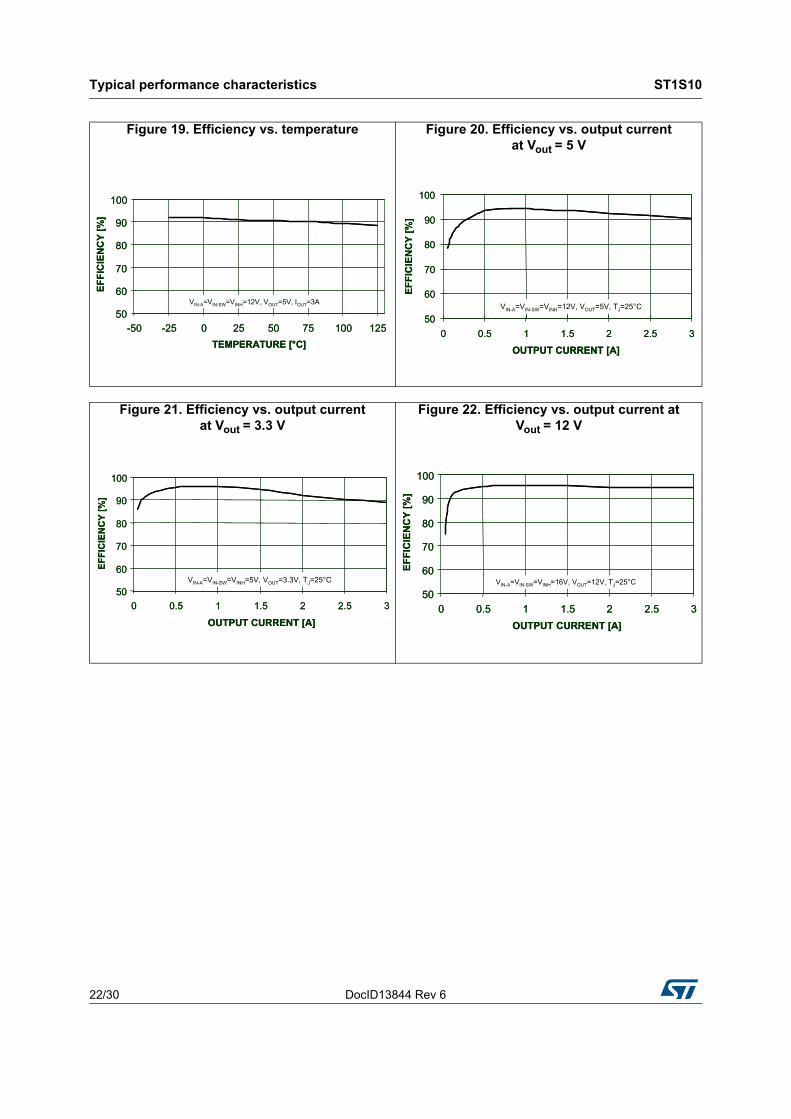
Figure 19. Efficiency vs. temperature Figure 20. Efficiency vs. output current at Vout = 5 V
50
60
70
80
90
100
-50 -25 0 25 50 75 100 125
TEMPERATURE [°C]
EF
FIC
IEN
CY
[%
]
VIN-A=VIN-SW=VINH=12V, VOUT=5V, IOUT=3A
50
60
70
80
90
100
-50 -25 0 25 50 75 100 125
TEMPERATURE [°C]
EF
FIC
IEN
CY
[%
]
VIN-A=VIN-SW=VINH=12V, VOUT=5V, IOUT=3A
50
60
70
80
90
100
0 0.5 1 1.5 2 2.5 3
OUTPUT CURRENT [A]
EF
FIC
IEN
CY
[%
]
VIN-A=VIN-SW=VINH=12V, VOUT=5V, TJ=25°C
50
60
70
80
90
100
0 0.5 1 1.5 2 2.5 3
OUTPUT CURRENT [A]
EF
FIC
IEN
CY
[%
]
VIN-A=VIN-SW=VINH=12V, VOUT=5V, TJ=25°C
Figure 21. Efficiency vs. output current at Vout = 3.3 V
Figure 22. Efficiency vs. output current at Vout = 12 V
50
60
70
80
90
100
0 0.5 1 1.5 2 2.5 3
OUTPUT CURRENT [A]
EF
FIC
IEN
CY
[%
]
VIN-A=VIN-SW=VINH=5V, VOUT=3.3V, TJ=25°C
50
60
70
80
90
100
0 0.5 1 1.5 2 2.5 3
OUTPUT CURRENT [A]
EF
FIC
IEN
CY
[%
]
VIN-A=VIN-SW=VINH=5V, VOUT=3.3V, TJ=25°C
50
60
70
80
90
100
0 0.5 1 1.5 2 2.5 3
OUTPUT CURRENT [A]
EF
FIC
IEN
CY
[%
]
VIN-A=VIN-SW=VINH=16V, VOUT=12V, TJ=25°C
50
60
70
80
90
100
0 0.5 1 1.5 2 2.5 3
OUTPUT CURRENT [A]
EF
FIC
IEN
CY
[%
]
VIN-A=VIN-SW=VINH=16V, VOUT=12V, TJ=25°C
DocID13844 Rev 6 23/30
ST1S10 Package information
30
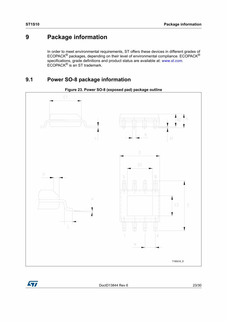
9 Package information
In order to meet environmental requirements, ST offers these devices in different grades of ECOPACK® packages, depending on their level of environmental compliance. ECOPACK® specifications, grade definitions and product status are available at: www.st.com. ECOPACK® is an ST trademark.
9.1 Power SO-8 package information
Figure 23. Power SO-8 (exposed pad) package outline
7195016_D
Package information ST1S10
24/30 DocID13844 Rev 6
Note: Dimension “D” does not include mold flash, protrusions or gate burrs. Mold flash, protrusions or gate burrs shall not exceed 0.15mm in total (both side).
Dimension “E1” does not include interlead flash or protrusions.
Interlead flash or protrusions shall not exceed 0.25mm per side.
The size of exposed pad is variable depending of leadframe design pad size.
End user should verify “D1” and “E2” dimensions for each device application.
Table 7. Power SO-8 (exposed pad) package mechanical data
SymbolDimensions (mm)
Min. Typ. Max.
A 1.70
A1 0.00 0.15
A2 1.25
b 0.31 0.51
c 0.17 0.25
D 4.80 4.90 5.00
D1 ACCORDING TO PAD SIZE
E 5.80 6.00 6.20
E1 3.80 3.90 4.00
E2 ACCORDING TO PAD SIZE
e 1.27
h 0.25 0.50
L 0.40 1.27
K 0 8
ccc 0.10
DocID13844 Rev 6 25/30
ST1S10 Package information
30
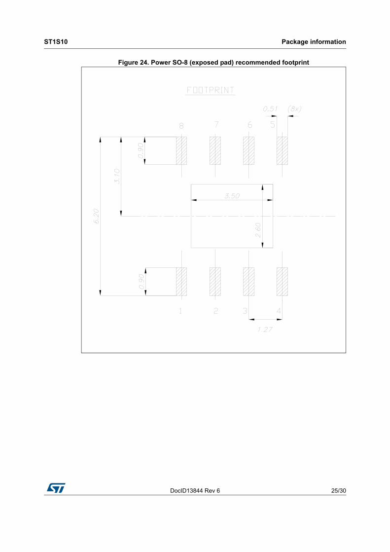
Figure 24. Power SO-8 (exposed pad) recommended footprint
Package information ST1S10
26/30 DocID13844 Rev 6
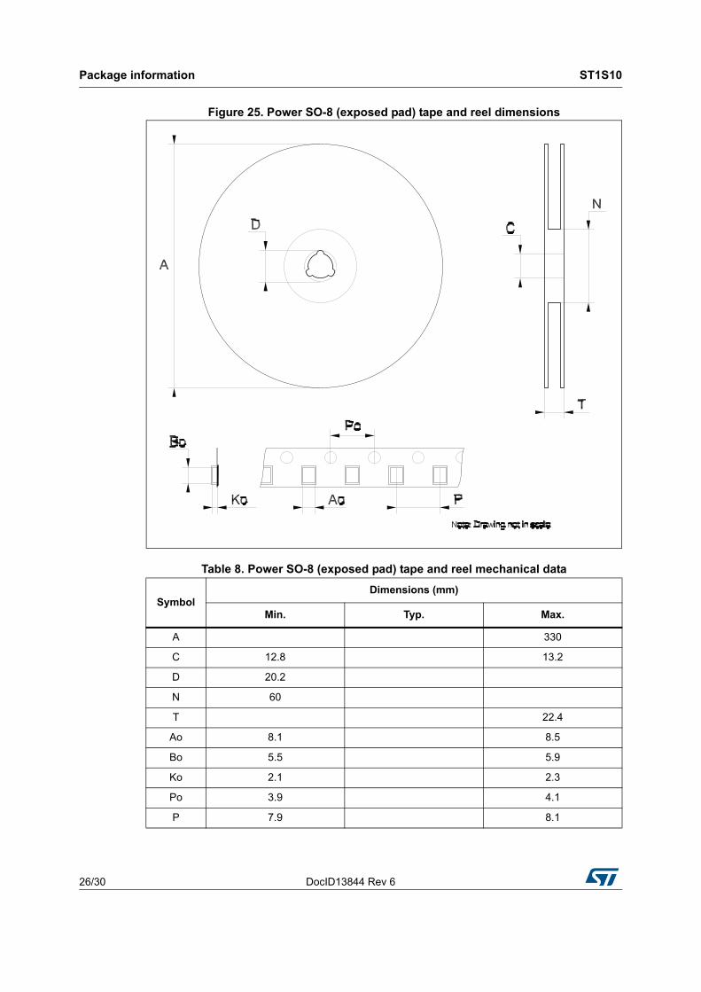
Figure 25. Power SO-8 (exposed pad) tape and reel dimensions
Table 8. Power SO-8 (exposed pad) tape and reel mechanical data
SymbolDimensions (mm)
Min. Typ. Max.
A 330
C 12.8 13.2
D 20.2
N 60
T 22.4
Ao 8.1 8.5
Bo 5.5 5.9
Ko 2.1 2.3
Po 3.9 4.1
P 7.9 8.1

DocID13844 Rev 6 27/30
ST1S10 Package information
30
9.2 DFN8 (4 x 4) package information
Figure 26. DFN8 (4 x 4) package outline
Table 9. DFN8 (4 x 4) package mechanical data
SymbolDimensions (mm)
Min. Typ. Max.
A 0.80 0.90 1.00
A1 0 0.02 0.05
A3 0.20
b 0.23 0.30 0.38
D 3.90 4.00 4.10
D2 2.82 3.00 3.23
E 3.90 4.00 4.10
E2 2.05 2.20 2.30
e 0.80
L 0.40 0.50 0.60
7869653B
Package information ST1S10
28/30 DocID13844 Rev 6
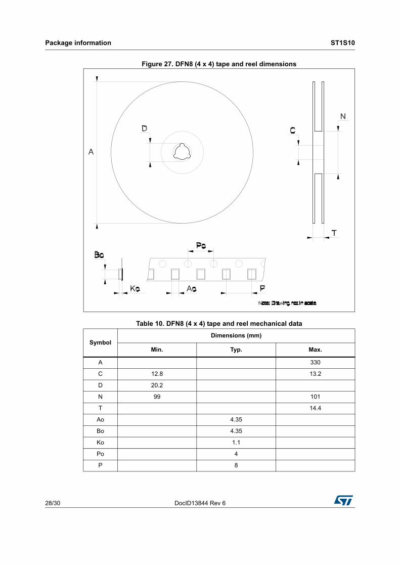
Figure 27. DFN8 (4 x 4) tape and reel dimensions
Table 10. DFN8 (4 x 4) tape and reel mechanical data
SymbolDimensions (mm)
Min. Typ. Max.
A 330
C 12.8 13.2
D 20.2
N 99 101
T 14.4
Ao 4.35
Bo 4.35
Ko 1.1
Po 4
P 8
DocID13844 Rev 6 29/30
ST1S10 Revision history
30
10 Revision history
Table 11. Document revision history
Date Revision Changes
28-Aug-2007 1 Initial release.
24-Sep-2007 2 Add RthJC on Table 4.
25-Oct-2007 3 Added new paragraph 6: Layout considerations.
16-Mar-2010 4 Updated PowerSO-8 package mechanical data.
31-May-2012 5Updated SO-8 (epad) and DFN8 (4x4) mechanical data.
Changed temperature min from 25 °C to 40 °C in Table 4, and in Section 4.
27-Mar-2015 6
Added Table 5: ESD protection on page 8.
Added and updated cross-references throughout document.
Updated titles of Figure 6 on page 17 and Figure 7 on page 18.
Updated Section 9: Package information on page 23 (updated/added titles, headers, reformatted section).
Minor modifications throughout document.
ST1S10
30/30 DocID13844 Rev 6
IMPORTANT NOTICE – PLEASE READ CAREFULLY
STMicroelectronics NV and its subsidiaries (“ST”) reserve the right to make changes, corrections, enhancements, modifications, and improvements to ST products and/or to this document at any time without notice. Purchasers should obtain the latest relevant information on ST products before placing orders. ST products are sold pursuant to ST’s terms and conditions of sale in place at the time of order acknowledgement.
Purchasers are solely responsible for the choice, selection, and use of ST products and ST assumes no liability for application assistance or the design of Purchasers’ products.
No license, express or implied, to any intellectual property right is granted by ST herein.
Resale of ST products with provisions different from the information set forth herein shall void any warranty granted by ST for such product.
ST and the ST logo are trademarks of ST. All other product or service names are the property of their respective owners.
Information in this document supersedes and replaces information previously supplied in any prior versions of this document.
© 2015 STMicroelectronics – All rights reserved