I/O Module v3.1
LogiCORE IP Product Guide
Vivado Design Suite
PG111 December 20, 2017
I/O Module v3.1 2PG111 December 20, 2017 www.xilinx.com
Table of ContentsIP Facts
Chapter 1: OverviewFeature Summary. . . . . . . . . . . . . . . . . . . . . . . . . . . . . . . . . . . . . . . . . . . . . . . . . . . . . . . . . . . . . . . . . . 6Licensing and Ordering . . . . . . . . . . . . . . . . . . . . . . . . . . . . . . . . . . . . . . . . . . . . . . . . . . . . . . . . . . . . . 8
Chapter 2: Product SpecificationStandards . . . . . . . . . . . . . . . . . . . . . . . . . . . . . . . . . . . . . . . . . . . . . . . . . . . . . . . . . . . . . . . . . . . . . . . . 9Performance. . . . . . . . . . . . . . . . . . . . . . . . . . . . . . . . . . . . . . . . . . . . . . . . . . . . . . . . . . . . . . . . . . . . . . 9Resource Utilization. . . . . . . . . . . . . . . . . . . . . . . . . . . . . . . . . . . . . . . . . . . . . . . . . . . . . . . . . . . . . . . 10Port Descriptions . . . . . . . . . . . . . . . . . . . . . . . . . . . . . . . . . . . . . . . . . . . . . . . . . . . . . . . . . . . . . . . . . 10Register Space . . . . . . . . . . . . . . . . . . . . . . . . . . . . . . . . . . . . . . . . . . . . . . . . . . . . . . . . . . . . . . . . . . . 12
Chapter 3: Designing with the CoreGeneral Design Guidelines . . . . . . . . . . . . . . . . . . . . . . . . . . . . . . . . . . . . . . . . . . . . . . . . . . . . . . . . . 23LMB Timing. . . . . . . . . . . . . . . . . . . . . . . . . . . . . . . . . . . . . . . . . . . . . . . . . . . . . . . . . . . . . . . . . . . . . . 28Clocking. . . . . . . . . . . . . . . . . . . . . . . . . . . . . . . . . . . . . . . . . . . . . . . . . . . . . . . . . . . . . . . . . . . . . . . . . 28Resets . . . . . . . . . . . . . . . . . . . . . . . . . . . . . . . . . . . . . . . . . . . . . . . . . . . . . . . . . . . . . . . . . . . . . . . . . . 29Protocol Description . . . . . . . . . . . . . . . . . . . . . . . . . . . . . . . . . . . . . . . . . . . . . . . . . . . . . . . . . . . . . . 29
Chapter 4: Design Flow StepsCustomizing and Generating the Core . . . . . . . . . . . . . . . . . . . . . . . . . . . . . . . . . . . . . . . . . . . . . . . . 30Constraining the Core . . . . . . . . . . . . . . . . . . . . . . . . . . . . . . . . . . . . . . . . . . . . . . . . . . . . . . . . . . . . . 43Simulation . . . . . . . . . . . . . . . . . . . . . . . . . . . . . . . . . . . . . . . . . . . . . . . . . . . . . . . . . . . . . . . . . . . . . . 44Synthesis and Implementation . . . . . . . . . . . . . . . . . . . . . . . . . . . . . . . . . . . . . . . . . . . . . . . . . . . . . . 44
Appendix A: UpgradingUpgrade . . . . . . . . . . . . . . . . . . . . . . . . . . . . . . . . . . . . . . . . . . . . . . . . . . . . . . . . . . . . . . . . . . . . . . . . 45
Appendix B: DebuggingFinding Help on Xilinx.com . . . . . . . . . . . . . . . . . . . . . . . . . . . . . . . . . . . . . . . . . . . . . . . . . . . . . . . . . 46Debug Tools . . . . . . . . . . . . . . . . . . . . . . . . . . . . . . . . . . . . . . . . . . . . . . . . . . . . . . . . . . . . . . . . . . . . . 47Simulation Debug. . . . . . . . . . . . . . . . . . . . . . . . . . . . . . . . . . . . . . . . . . . . . . . . . . . . . . . . . . . . . . . . . 48
Send Feedback
I/O Module v3.1 3PG111 December 20, 2017 www.xilinx.com
Hardware Debug . . . . . . . . . . . . . . . . . . . . . . . . . . . . . . . . . . . . . . . . . . . . . . . . . . . . . . . . . . . . . . . . . 48
Appendix C: Application Software DevelopmentDevice Drivers . . . . . . . . . . . . . . . . . . . . . . . . . . . . . . . . . . . . . . . . . . . . . . . . . . . . . . . . . . . . . . . . . . . 50
Appendix D: Additional Resources and Legal NoticesXilinx Resources . . . . . . . . . . . . . . . . . . . . . . . . . . . . . . . . . . . . . . . . . . . . . . . . . . . . . . . . . . . . . . . . . . 51References . . . . . . . . . . . . . . . . . . . . . . . . . . . . . . . . . . . . . . . . . . . . . . . . . . . . . . . . . . . . . . . . . . . . . . 51Revision History . . . . . . . . . . . . . . . . . . . . . . . . . . . . . . . . . . . . . . . . . . . . . . . . . . . . . . . . . . . . . . . . . . 52Please Read: Important Legal Notices . . . . . . . . . . . . . . . . . . . . . . . . . . . . . . . . . . . . . . . . . . . . . . . . 52
Send Feedback
I/O Module v3.1 4PG111 December 20, 2017 www.xilinx.com Product Specification
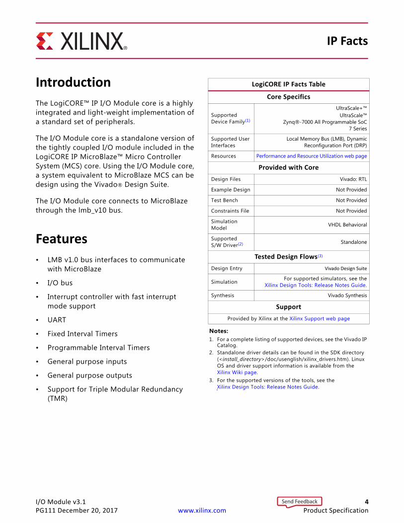
IntroductionThe LogiCORE™ IP I/O Module core is a highly integrated and light-weight implementation of a standard set of peripherals.
The I/O Module core is a standalone version of the tightly coupled I/O module included in the LogiCORE IP MicroBlaze™ Micro Controller System (MCS) core. Using the I/O Module core, a system equivalent to MicroBlaze MCS can be design using the Vivado® Design Suite.
The I/O Module core connects to MicroBlaze through the lmb_v10 bus.
Features• LMB v1.0 bus interfaces to communicate
with MicroBlaze
• I/O bus
• Interrupt controller with fast interrupt mode support
• UART
• Fixed Interval Timers
• Programmable Interval Timers
• General purpose inputs
• General purpose outputs
• Support for Triple Modular Redundancy (TMR)
IP Facts
LogiCORE IP Facts Table
Core Specifics
Supported Device Family(1)
UltraScale+™UltraScale™
Zynq®-7000 All Programmable SoC7 Series
Supported User Interfaces
Local Memory Bus (LMB), DynamicReconfiguration Port (DRP)
Resources Performance and Resource Utilization web page
Provided with CoreDesign Files Vivado: RTL
Example Design Not Provided
Test Bench Not Provided
Constraints File Not Provided
Simulation Model VHDL Behavioral
Supported S/W Driver(2) Standalone
Tested Design Flows(3)
Design Entry Vivado Design Suite
Simulation For supported simulators, see theXilinx Design Tools: Release Notes Guide.
Synthesis Vivado Synthesis
SupportProvided by Xilinx at the Xilinx Support web page
Notes: 1. For a complete listing of supported devices, see the Vivado IP
Catalog.2. Standalone driver details can be found in the SDK directory
(<install_directory>/doc/usenglish/xilinx_drivers.htm). Linux OS and driver support information is available from theXilinx Wiki page.
3. For the supported versions of the tools, see theXilinx Design Tools: Release Notes Guide.
Send Feedback
I/O Module v3.1 5PG111 December 20, 2017 www.xilinx.com
Chapter 1
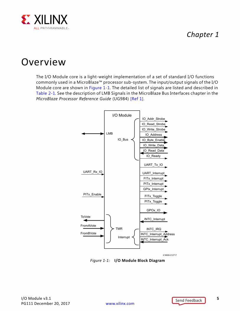
OverviewThe I/O Module core is a light-weight implementation of a set of standard I/O functions commonly used in a MicroBlaze™ processor sub-system. The input/output signals of the I/O Module core are shown in Figure 1-1. The detailed list of signals are listed and described in Table 2-1. See the description of LMB Signals in the MicroBlaze Bus Interfaces chapter in the MicroBlaze Processor Reference Guide (UG984) [Ref 1].
.X-Ref Target - Figure 1-1
Figure 1-1: I/O Module Block Diagram
I/O Module
LMB
UART_Rx_IO
PITx_Enable
FromAVote
IO_Addr_Strobe
IO_Read_Strobe
IO_Write_Strobe
IO_Address
IO_Byte_Enable
IO_Write_Data
IO_Read_Data
IO_Ready
UART_Tx_IO
UART_Interrupt
FITx_Interrupt
PITx_Interrupt
GPIx_Interrupt
FITx_Toggle
PITx_Toggle
GPOx_IO
INTC_Interrupt
INTC_IRQINTC_Interrupt_Address
INTC_Interrupt_Ack
IO_Bus
Interrupt
ToVote
FromBVoteTMR
Send Feedback
I/O Module v3.1 6PG111 December 20, 2017 www.xilinx.com
Chapter 1: Overview
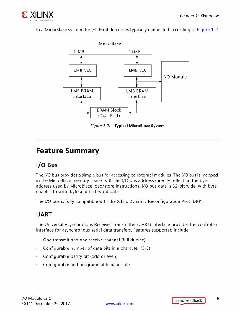
In a MicroBlaze system the I/O Module core is typically connected according to Figure 1-2.
Feature Summary
I/O BusThe I/O bus provides a simple bus for accessing to external modules. The I/O bus is mapped in the MicroBlaze memory space, with the I/O bus address directly reflecting the byte address used by MicroBlaze load/store instructions. I/O bus data is 32-bit wide, with byte enables to write byte and half-word data.
The I/O bus is fully compatible with the Xilinx Dynamic Reconfiguration Port (DRP).
UARTThe Universal Asynchronous Receiver Transmitter (UART) interface provides the controller interface for asynchronous serial data transfers. Features supported include:
• One transmit and one receive channel (full duplex)
• Configurable number of data bits in a character (5-8)
• Configurable parity bit (odd or even)
• Configurable and programmable baud rate
X-Ref Target - Figure 1-2
Figure 1-2: Typical MicroBlaze System
ILMB
MicroBlaze
LMB_v10
LMB BRAMInterface
BRAM Block(Dual Port)
DLMB
LMB_v10
LMB BRAMInterface
I/O Module
Send Feedback
I/O Module v3.1 7PG111 December 20, 2017 www.xilinx.com
Chapter 1: Overview
Fixed Interval TimerThe Fixed Interval Timer (FIT) generates a strobe signal at fixed intervals. The Fixed Interval Timer asserts the output signal and generates an interrupt according to the selected parameter values.
Programmable Interval TimerThe Programmable Interval Timer (PIT) has a configurable width from 1 to 32. The PIT operation and period are controlled by software. An interrupt can be generated when the timer expires.
General Purpose OutputThe General Purpose Output (GPO) drives I/O Module GPO output signals defined by the value of the corresponding GPO register, programmable from software. The width and initial value are defined by parameters.
General Purpose Input The General Purpose Input (GPI) makes it possible for software to sample the value of the I/O Module GPI input signals by reading the GPI register. The width and whether to generate an interrupt are defined by parameters.
Interrupt ControllerThe Interrupt Controller (INTC) handles both I/O module internal interrupt events and external ones. The internal interrupt events originate from the UART, the Fixed Interval Timers, the Programmable Interval Timers, or the General Purpose Inputs.
Triple Modular RedundancyWhen enabling Triple Modular Redundancy (TMR), the I/O Module performs majority voting on all internal registers. The voting is performed between the internal value, and the register values from the two other I/O Module cores in a triplicated sub-system, by using the voting signals interconnecting the cores.
This functionality is intended to be used together with the TMR IP cores, which provide a complete TMR solution. See Triple Modular Redundancy (TMR) (PG268) [Ref 3] for details.
Send Feedback
I/O Module v3.1 8PG111 December 20, 2017 www.xilinx.com
Chapter 1: Overview
Licensing and OrderingThis Xilinx® LogiCORE™ IP module is provided at no additional cost with the Xilinx Vivado® Design Suite under the terms of the Xilinx End User License. Information about this and other Xilinx LogiCORE IP modules is available at the Xilinx Intellectual Property page. For information about pricing and availability of other Xilinx LogiCORE IP modules and tools, contact your local Xilinx sales representative.
Send Feedback
I/O Module v3.1 9PG111 December 20, 2017 www.xilinx.com
Chapter 2
Product Specification
StandardsThe I/O bus interface provided by the I/O Module core is fully compatible with the Xilinx Dynamic Reconfiguration Port (DRP). For a detailed description of the DRP, see the 7 Series FPGAs Configuration User Guide (UG740) [Ref 2].
PerformanceThe frequency and latency of the I/O Module core are optimized for use together with MicroBlaze™. This means that the frequency targets are aligned to MicroBlaze targets as well as the access latency optimized for MicroBlaze data access.
Maximum FrequenciesFor details about performance, visit Performance and Resource Utilization.
Latency• Data read from I/O Module core registers is available two clock cycles after the address
strobe is asserted.
• Data write to I/O Module core registers is performed the clock cycle after the address strobe is asserted.
• Data accesses to peripherals connected on the I/O bus take three clock cycles plus the number of wait states introduced by the accessed peripheral.
ThroughputThe maximum throughput when using the I/O bus is one read or write access every three clock cycles.
Send Feedback
I/O Module v3.1 10PG111 December 20, 2017 www.xilinx.com
Chapter 2: Product Specification
Resource UtilizationFor details about resource utilization, visit Performance and Resource Utilization.
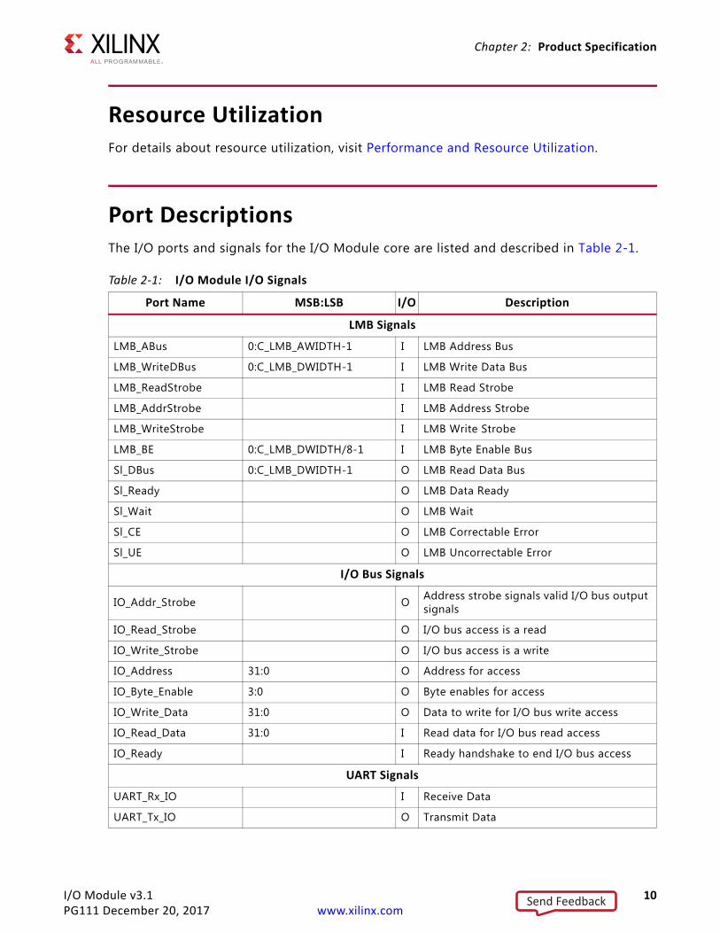
Port DescriptionsThe I/O ports and signals for the I/O Module core are listed and described in Table 2-1.
Table 2-1: I/O Module I/O Signals
Port Name MSB:LSB I/O Description
LMB Signals
LMB_ABus 0:C_LMB_AWIDTH-1 I LMB Address Bus
LMB_WriteDBus 0:C_LMB_DWIDTH-1 I LMB Write Data Bus
LMB_ReadStrobe I LMB Read Strobe
LMB_AddrStrobe I LMB Address Strobe
LMB_WriteStrobe I LMB Write Strobe
LMB_BE 0:C_LMB_DWIDTH/8-1 I LMB Byte Enable Bus
Sl_DBus 0:C_LMB_DWIDTH-1 O LMB Read Data Bus
Sl_Ready O LMB Data Ready
Sl_Wait O LMB Wait
Sl_CE O LMB Correctable Error
Sl_UE O LMB Uncorrectable Error
I/O Bus Signals
IO_Addr_Strobe O Address strobe signals valid I/O bus output signals
IO_Read_Strobe O I/O bus access is a read
IO_Write_Strobe O I/O bus access is a write
IO_Address 31:0 O Address for access
IO_Byte_Enable 3:0 O Byte enables for access
IO_Write_Data 31:0 O Data to write for I/O bus write access
IO_Read_Data 31:0 I Read data for I/O bus read access
IO_Ready I Ready handshake to end I/O bus access
UART Signals
UART_Rx_IO I Receive Data
UART_Tx_IO O Transmit Data
Send Feedback
I/O Module v3.1 11PG111 December 20, 2017 www.xilinx.com
Chapter 2: Product Specification
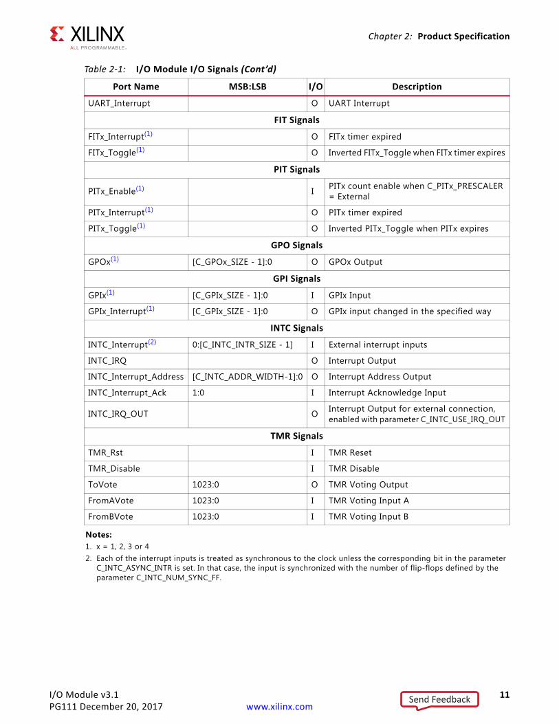
UART_Interrupt O UART Interrupt
FIT Signals
FITx_Interrupt(1) O FITx timer expired
FITx_Toggle(1) O Inverted FITx_Toggle when FITx timer expires
PIT Signals
PITx_Enable(1) I PITx count enable when C_PITx_PRESCALER = External
PITx_Interrupt(1) O PITx timer expired
PITx_Toggle(1) O Inverted PITx_Toggle when PITx expires
GPO Signals
GPOx(1) [C_GPOx_SIZE - 1]:0 O GPOx Output
GPI Signals
GPIx(1) [C_GPIx_SIZE - 1]:0 I GPIx Input
GPIx_Interrupt(1) [C_GPIx_SIZE - 1]:0 O GPIx input changed in the specified way
INTC Signals
INTC_Interrupt(2) 0:[C_INTC_INTR_SIZE - 1] I External interrupt inputs
INTC_IRQ O Interrupt Output
INTC_Interrupt_Address [C_INTC_ADDR_WIDTH-1]:0 O Interrupt Address Output
INTC_Interrupt_Ack 1:0 I Interrupt Acknowledge Input
INTC_IRQ_OUT O Interrupt Output for external connection, enabled with parameter C_INTC_USE_IRQ_OUT
TMR Signals
TMR_Rst I TMR Reset
TMR_Disable I TMR Disable
ToVote 1023:0 O TMR Voting Output
FromAVote 1023:0 I TMR Voting Input A
FromBVote 1023:0 I TMR Voting Input B
Notes: 1. x = 1, 2, 3 or 42. Each of the interrupt inputs is treated as synchronous to the clock unless the corresponding bit in the parameter
C_INTC_ASYNC_INTR is set. In that case, the input is synchronized with the number of flip-flops defined by the parameter C_INTC_NUM_SYNC_FF.
Table 2-1: I/O Module I/O Signals (Cont’d)
Port Name MSB:LSB I/O Description
Send Feedback
I/O Module v3.1 12PG111 December 20, 2017 www.xilinx.com
Chapter 2: Product Specification
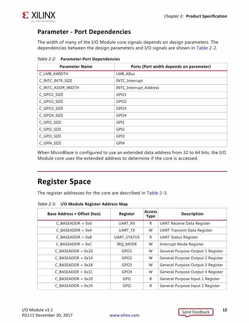
Parameter - Port DependenciesThe width of many of the I/O Module core signals depends on design parameters. The dependencies between the design parameters and I/O signals are shown in Table 2-2.
When MicroBlaze is configured to use an extended data address from 32 to 64 bits, the I/O Module core uses the extended address to determine if the core is accessed.
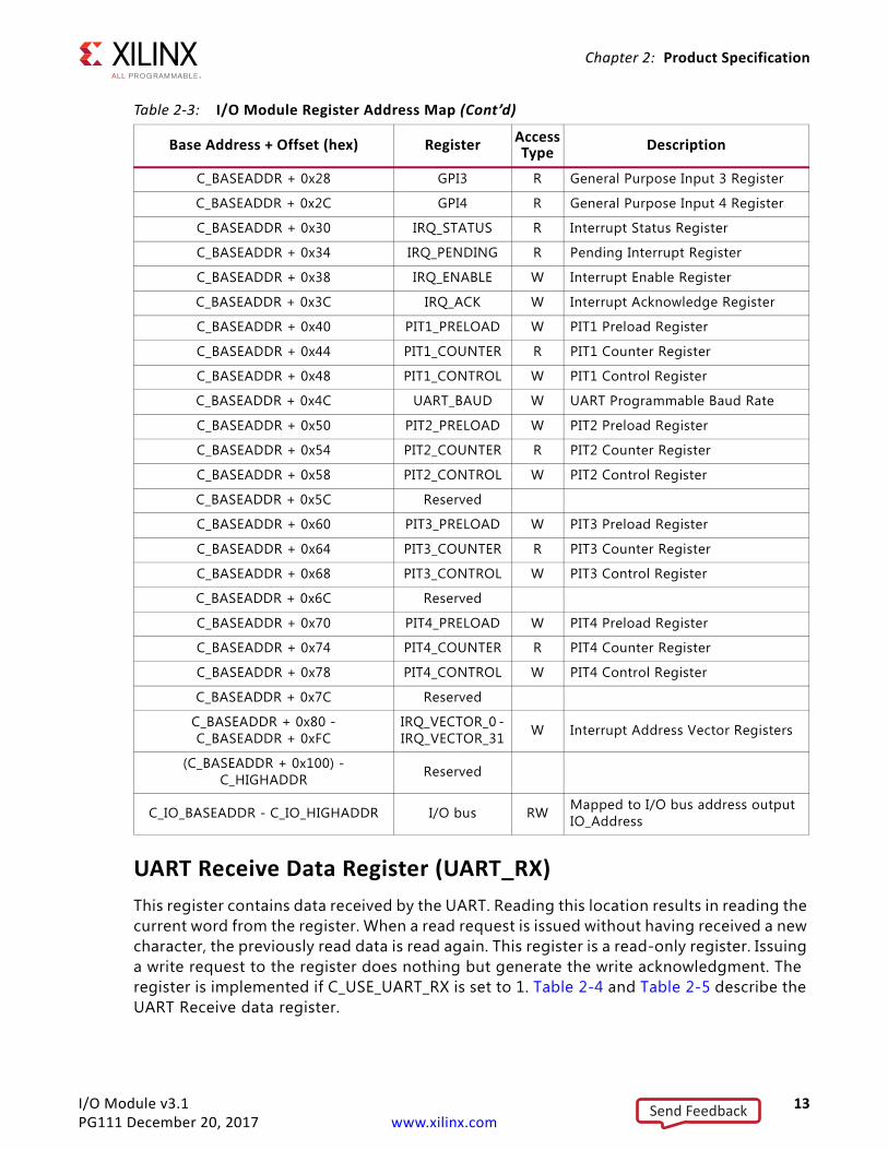
Register SpaceThe register addresses for the core are described in Table 2-3.
Table 2-2: Parameter-Port Dependencies
Parameter Name Ports (Port width depends on parameter)C_LMB_AWIDTH LMB_ABus
C_INTC_INTR_SIZE INTC_Interrupt
C_INTC_ADDR_WIDTH INTC_Interrupt_Address
C_GPO1_SIZE GPO1
C_GPO2_SIZE GPO2
C_GPO3_SIZE GPO3
C_GPO4_SIZE GPO4
C_GPI1_SIZE GPI1
C_GPI2_SIZE GPI2
C_GPI3_SIZE GPI3
C_GPI4_SIZE GPI4
Table 2-3: I/O Module Register Address Map
Base Address + Offset (hex) Register AccessType Description
C_BASEADDR + 0x0 UART_RX R UART Receive Data Register
C_BASEADDR + 0x4 UART_TX W UART Transmit Data Register
C_BASEADDR + 0x8 UART_STATUS R UART Status Register
C_BASEADDR + 0xC IRQ_MODE W Interrupt Mode Register
C_BASEADDR + 0x10 GPO1 W General Purpose Output 1 Register
C_BASEADDR + 0x14 GPO2 W General Purpose Output 2 Register
C_BASEADDR + 0x18 GPO3 W General Purpose Output 3 Register
C_BASEADDR + 0x1C GPO4 W General Purpose Output 4 Register
C_BASEADDR + 0x20 GPI1 R General Purpose Input 1 Register
C_BASEADDR + 0x24 GPI2 R General Purpose Input 2 Register
Send Feedback
I/O Module v3.1 13PG111 December 20, 2017 www.xilinx.com
Chapter 2: Product Specification
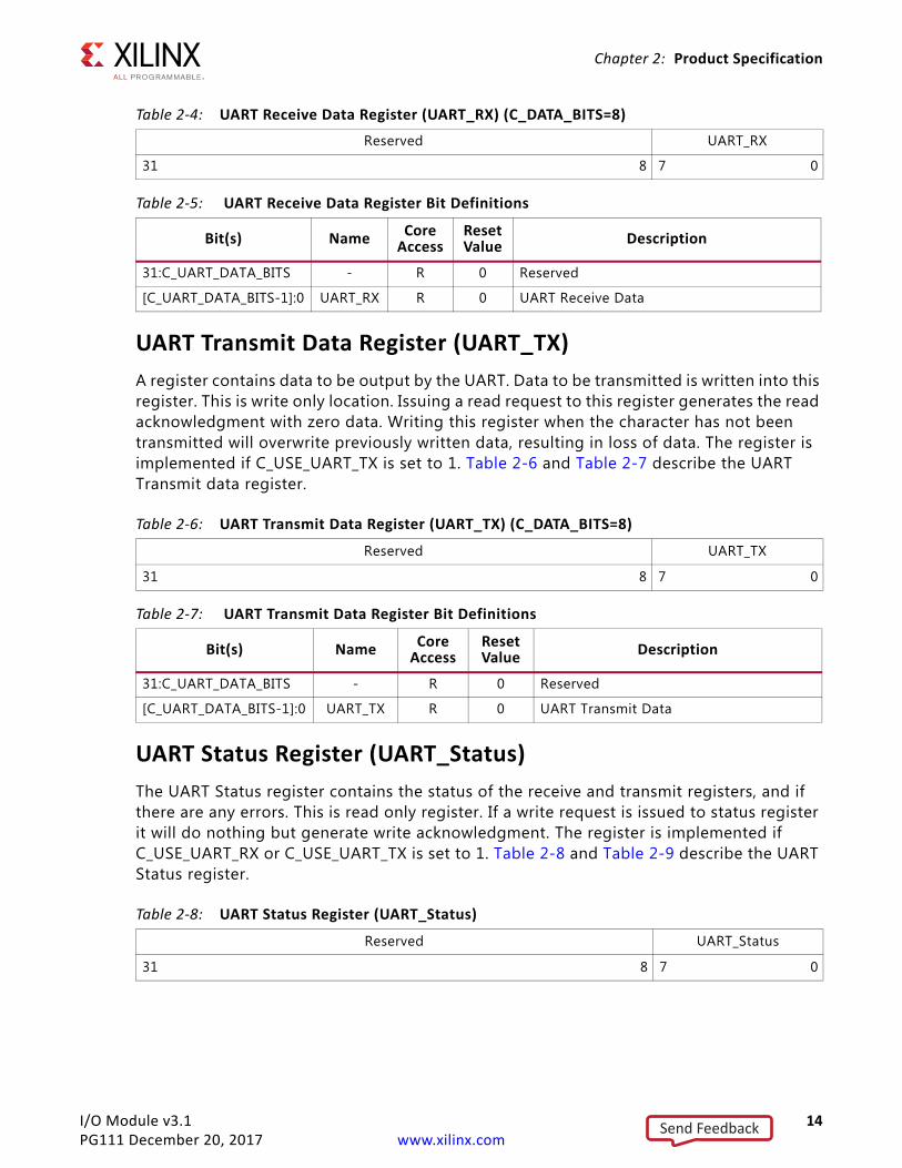
UART Receive Data Register (UART_RX)This register contains data received by the UART. Reading this location results in reading the current word from the register. When a read request is issued without having received a new character, the previously read data is read again. This register is a read-only register. Issuing a write request to the register does nothing but generate the write acknowledgment. The register is implemented if C_USE_UART_RX is set to 1. Table 2-4 and Table 2-5 describe the UART Receive data register.
C_BASEADDR + 0x28 GPI3 R General Purpose Input 3 Register
C_BASEADDR + 0x2C GPI4 R General Purpose Input 4 Register
C_BASEADDR + 0x30 IRQ_STATUS R Interrupt Status Register
C_BASEADDR + 0x34 IRQ_PENDING R Pending Interrupt Register
C_BASEADDR + 0x38 IRQ_ENABLE W Interrupt Enable Register
C_BASEADDR + 0x3C IRQ_ACK W Interrupt Acknowledge Register
C_BASEADDR + 0x40 PIT1_PRELOAD W PIT1 Preload Register
C_BASEADDR + 0x44 PIT1_COUNTER R PIT1 Counter Register
C_BASEADDR + 0x48 PIT1_CONTROL W PIT1 Control Register
C_BASEADDR + 0x4C UART_BAUD W UART Programmable Baud Rate
C_BASEADDR + 0x50 PIT2_PRELOAD W PIT2 Preload Register
C_BASEADDR + 0x54 PIT2_COUNTER R PIT2 Counter Register
C_BASEADDR + 0x58 PIT2_CONTROL W PIT2 Control Register
C_BASEADDR + 0x5C Reserved
C_BASEADDR + 0x60 PIT3_PRELOAD W PIT3 Preload Register
C_BASEADDR + 0x64 PIT3_COUNTER R PIT3 Counter Register
C_BASEADDR + 0x68 PIT3_CONTROL W PIT3 Control Register
C_BASEADDR + 0x6C Reserved
C_BASEADDR + 0x70 PIT4_PRELOAD W PIT4 Preload Register
C_BASEADDR + 0x74 PIT4_COUNTER R PIT4 Counter Register
C_BASEADDR + 0x78 PIT4_CONTROL W PIT4 Control Register
C_BASEADDR + 0x7C Reserved
C_BASEADDR + 0x80 -C_BASEADDR + 0xFC
IRQ_VECTOR_0 -IRQ_VECTOR_31 W Interrupt Address Vector Registers
(C_BASEADDR + 0x100) - C_HIGHADDR Reserved
C_IO_BASEADDR - C_IO_HIGHADDR I/O bus RW Mapped to I/O bus address outputIO_Address
Table 2-3: I/O Module Register Address Map (Cont’d)
Base Address + Offset (hex) Register AccessType Description
Send Feedback
I/O Module v3.1 14PG111 December 20, 2017 www.xilinx.com
Chapter 2: Product Specification
UART Transmit Data Register (UART_TX)A register contains data to be output by the UART. Data to be transmitted is written into this register. This is write only location. Issuing a read request to this register generates the read acknowledgment with zero data. Writing this register when the character has not been transmitted will overwrite previously written data, resulting in loss of data. The register is implemented if C_USE_UART_TX is set to 1. Table 2-6 and Table 2-7 describe the UART Transmit data register.
UART Status Register (UART_Status)The UART Status register contains the status of the receive and transmit registers, and if there are any errors. This is read only register. If a write request is issued to status register it will do nothing but generate write acknowledgment. The register is implemented if C_USE_UART_RX or C_USE_UART_TX is set to 1. Table 2-8 and Table 2-9 describe the UART Status register.
Table 2-4: UART Receive Data Register (UART_RX) (C_DATA_BITS=8)Reserved UART_RX
31 8 7 0
Table 2-5: UART Receive Data Register Bit Definitions
Bit(s) Name CoreAccess
ResetValue Description
31:C_UART_DATA_BITS - R 0 Reserved
[C_UART_DATA_BITS-1]:0 UART_RX R 0 UART Receive Data
Table 2-6: UART Transmit Data Register (UART_TX) (C_DATA_BITS=8)
Reserved UART_TX
31 8 7 0
Table 2-7: UART Transmit Data Register Bit Definitions
Bit(s) Name CoreAccess
ResetValue Description
31:C_UART_DATA_BITS - R 0 Reserved
[C_UART_DATA_BITS-1]:0 UART_TX R 0 UART Transmit Data
Table 2-8: UART Status Register (UART_Status)
Reserved UART_Status
31 8 7 0
Send Feedback
I/O Module v3.1 15PG111 December 20, 2017 www.xilinx.com
Chapter 2: Product Specification
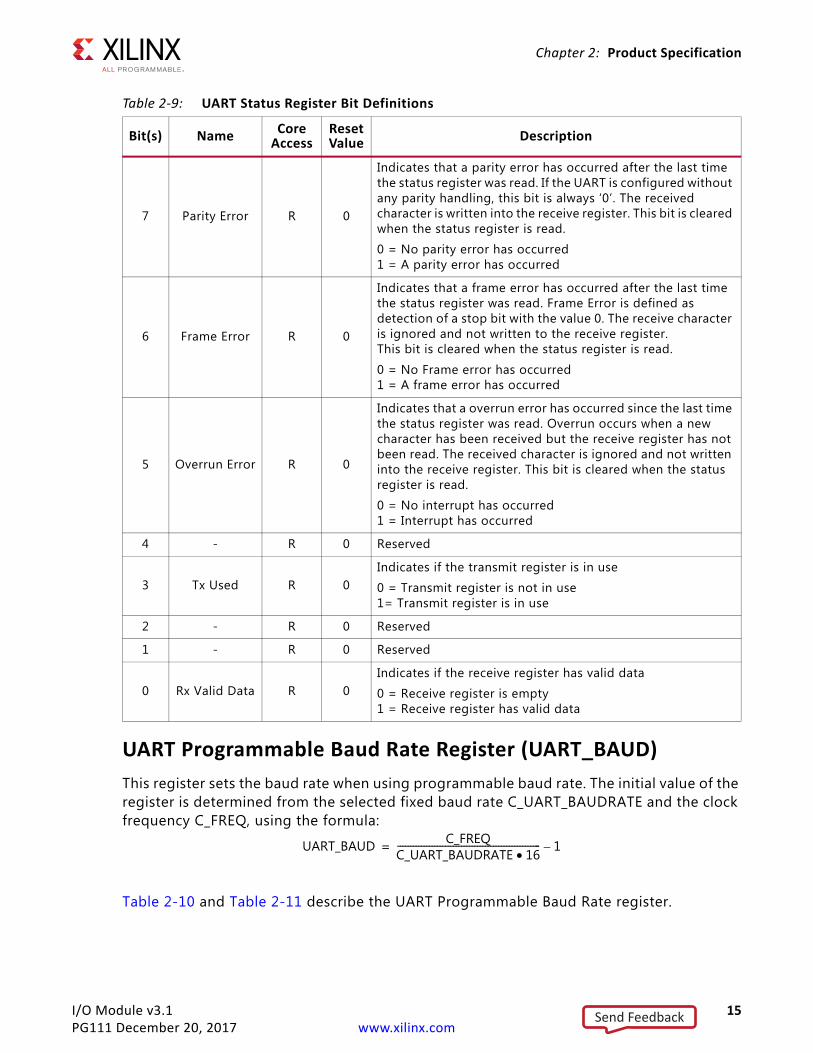
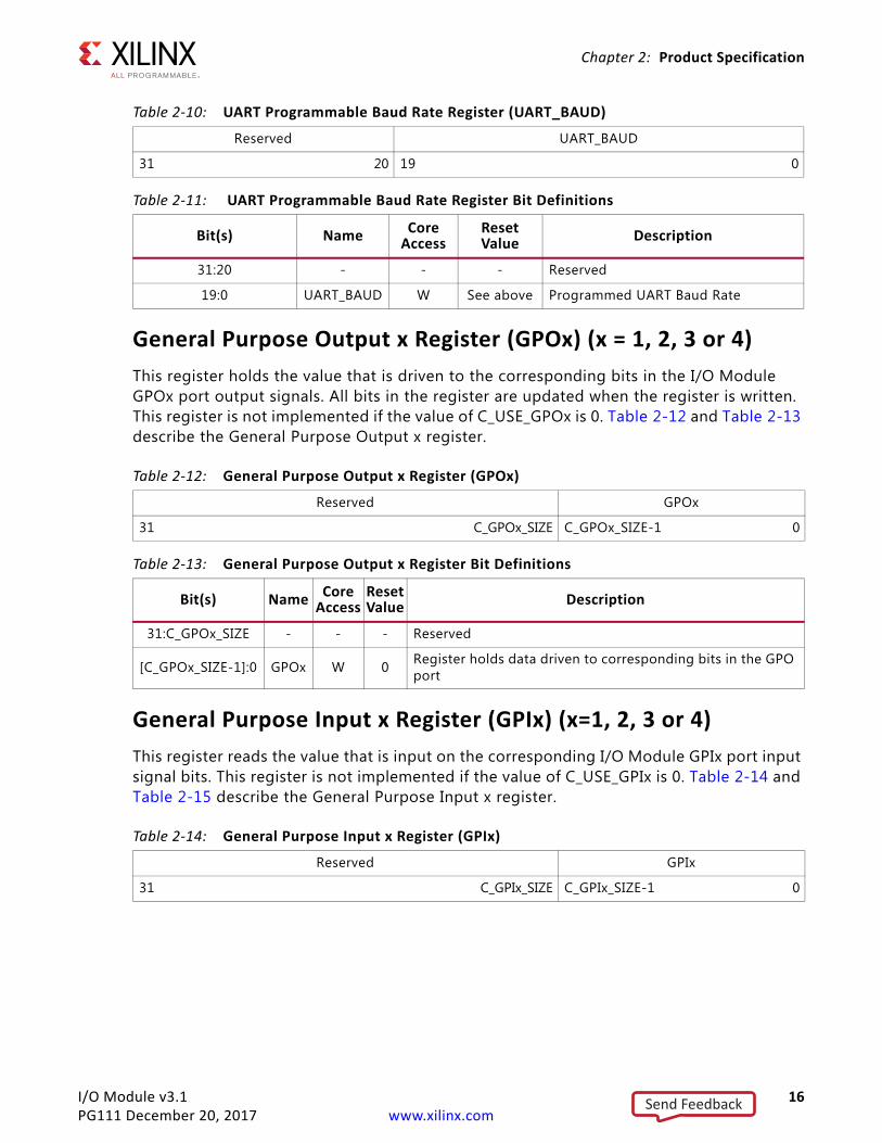
UART Programmable Baud Rate Register (UART_BAUD)This register sets the baud rate when using programmable baud rate. The initial value of the register is determined from the selected fixed baud rate C_UART_BAUDRATE and the clock frequency C_FREQ, using the formula:
Table 2-10 and Table 2-11 describe the UART Programmable Baud Rate register.
Table 2-9: UART Status Register Bit Definitions
Bit(s) Name CoreAccess
ResetValue Description
7 Parity Error R 0
Indicates that a parity error has occurred after the last time the status register was read. If the UART is configured without any parity handling, this bit is always ‘0’. The received character is written into the receive register. This bit is cleared when the status register is read.
0 = No parity error has occurred1 = A parity error has occurred
6 Frame Error R 0
Indicates that a frame error has occurred after the last time the status register was read. Frame Error is defined as detection of a stop bit with the value 0. The receive character is ignored and not written to the receive register. This bit is cleared when the status register is read.
0 = No Frame error has occurred1 = A frame error has occurred
5 Overrun Error R 0
Indicates that a overrun error has occurred since the last time the status register was read. Overrun occurs when a new character has been received but the receive register has not been read. The received character is ignored and not written into the receive register. This bit is cleared when the status register is read.
0 = No interrupt has occurred1 = Interrupt has occurred
4 - R 0 Reserved
3 Tx Used R 0Indicates if the transmit register is in use
0 = Transmit register is not in use1= Transmit register is in use
2 - R 0 Reserved
1 - R 0 Reserved
0 Rx Valid Data R 0Indicates if the receive register has valid data
0 = Receive register is empty1 = Receive register has valid data
UART_BAUD C_FREQC_UART_BAUDRATE 16•------------------------------------------------------ 1–=
Send Feedback
I/O Module v3.1 16PG111 December 20, 2017 www.xilinx.com
Chapter 2: Product Specification
General Purpose Output x Register (GPOx) (x = 1, 2, 3 or 4)This register holds the value that is driven to the corresponding bits in the I/O Module GPOx port output signals. All bits in the register are updated when the register is written. This register is not implemented if the value of C_USE_GPOx is 0. Table 2-12 and Table 2-13 describe the General Purpose Output x register.
General Purpose Input x Register (GPIx) (x=1, 2, 3 or 4)This register reads the value that is input on the corresponding I/O Module GPIx port input signal bits. This register is not implemented if the value of C_USE_GPIx is 0. Table 2-14 and Table 2-15 describe the General Purpose Input x register.
Table 2-10: UART Programmable Baud Rate Register (UART_BAUD)
Reserved UART_BAUD
31 20 19 0
Table 2-11: UART Programmable Baud Rate Register Bit Definitions
Bit(s) Name CoreAccess
ResetValue Description
31:20 - - - Reserved
19:0 UART_BAUD W See above Programmed UART Baud Rate
Table 2-12: General Purpose Output x Register (GPOx)
Reserved GPOx
31 C_GPOx_SIZE C_GPOx_SIZE-1 0
Table 2-13: General Purpose Output x Register Bit Definitions
Bit(s) Name CoreAccess
ResetValue Description
31:C_GPOx_SIZE - - - Reserved
[C_GPOx_SIZE-1]:0 GPOx W 0 Register holds data driven to corresponding bits in the GPO port
Table 2-14: General Purpose Input x Register (GPIx)
Reserved GPIx
31 C_GPIx_SIZE C_GPIx_SIZE-1 0
Send Feedback
I/O Module v3.1 17PG111 December 20, 2017 www.xilinx.com
Chapter 2: Product Specification
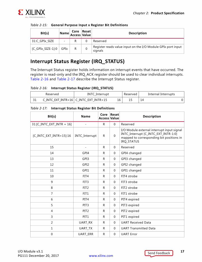
Interrupt Status Register (IRQ_STATUS)The Interrupt Status register holds information on interrupt events that have occurred. The register is read-only and the IRQ_ACK register should be used to clear individual interrupts. Table 2-16 and Table 2-17 describe the Interrupt Status register.
Table 2-15: General Purpose Input x Register Bit Definitions
Bit(s) Name CoreAccess
ResetValue Description
31:C_GPIx_SIZE - R 0 Reserved
[C_GPIx_SIZE-1]:0 GPIx R 0 Register reads value input on the I/O Module GPIx port input signals
Table 2-16: Interrupt Status Register (IRQ_STATUS)
Reserved INTC_Interrupt Reserved Internal Interrupts
31 C_INTC_EXT_INTR+16 C_INTC_EXT_INTR+15 16 15 14 0
Table 2-17: Interrupt Status Register Bit Definitions
Bit(s) Name CoreAccess
ResetValue Description
31:[C_INTC_EXT_INTR + 16] - R 0 Reserved
[C_INTC_EXT_INTR+15]:16 INTC_Interrupt R 0
I/O Module external interrupt input signal INTC_Interrupt [C_INTC_EXT_INTR-1:0] mapped to corresponding bit positions in IRQ_STATUS
15 - R 0 Reserved
14 GPI4 R 0 GPI4 changed
13 GPI3 R 0 GPI3 changed
12 GPI2 R 0 GPI2 changed
11 GPI1 R 0 GPI1 changed
10 FIT4 R 0 FIT4 strobe
9 FIT3 R 0 FIT3 strobe
8 FIT2 R 0 FIT2 strobe
7 FIT1 R 0 FIT1 strobe
6 PIT4 R 0 PIT4 expired
5 PIT3 R 0 PIT3 expired
4 PIT2 R 0 PIT2 expired
3 PIT1 R 0 PIT1 expired
2 UART_RX R 0 UART Received Data
1 UART_TX R 0 UART Transmitted Data
0 UART_ERR R 0 UART Error
Send Feedback
I/O Module v3.1 18PG111 December 20, 2017 www.xilinx.com
Chapter 2: Product Specification
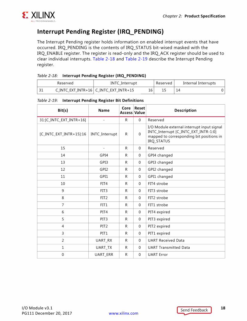
Interrupt Pending Register (IRQ_PENDING)The Interrupt Pending register holds information on enabled interrupt events that have occurred. IRQ_PENDING is the contents of IRQ_STATUS bit-wised masked with the IRQ_ENABLE register. The register is read-only and the IRQ_ACK register should be used to clear individual interrupts. Table 2-18 and Table 2-19 describe the Interrupt Pending register.
Table 2-18: Interrupt Pending Register (IRQ_PENDING)
Reserved INTC_Interrupt Reserved Internal Interrupts
31 C_INTC_EXT_INTR+16 C_INTC_EXT_INTR+15 16 15 14 0
Table 2-19: Interrupt Pending Register Bit Definitions
Bit(s) Name CoreAccess
ResetValue Description
31:[C_INTC_EXT_INTR+16] - R 0 Reserved
[C_INTC_EXT_INTR+15]:16 INTC_Interrupt R 0
I/O Module external interrupt input signal INTC_Interrupt [C_INTC_EXT_INTR-1:0] mapped to corresponding bit positions in IRQ_STATUS
15 - R 0 Reserved
14 GPI4 R 0 GPI4 changed
13 GPI3 R 0 GPI3 changed
12 GPI2 R 0 GPI2 changed
11 GPI1 R 0 GPI1 changed
10 FIT4 R 0 FIT4 strobe
9 FIT3 R 0 FIT3 strobe
8 FIT2 R 0 FIT2 strobe
7 FIT1 R 0 FIT1 strobe
6 PIT4 R 0 PIT4 expired
5 PIT3 R 0 PIT3 expired
4 PIT2 R 0 PIT2 expired
3 PIT1 R 0 PIT1 expired
2 UART_RX R 0 UART Received Data
1 UART_TX R 0 UART Transmitted Data
0 UART_ERR R 0 UART Error
Send Feedback
I/O Module v3.1 19PG111 December 20, 2017 www.xilinx.com
Chapter 2: Product Specification
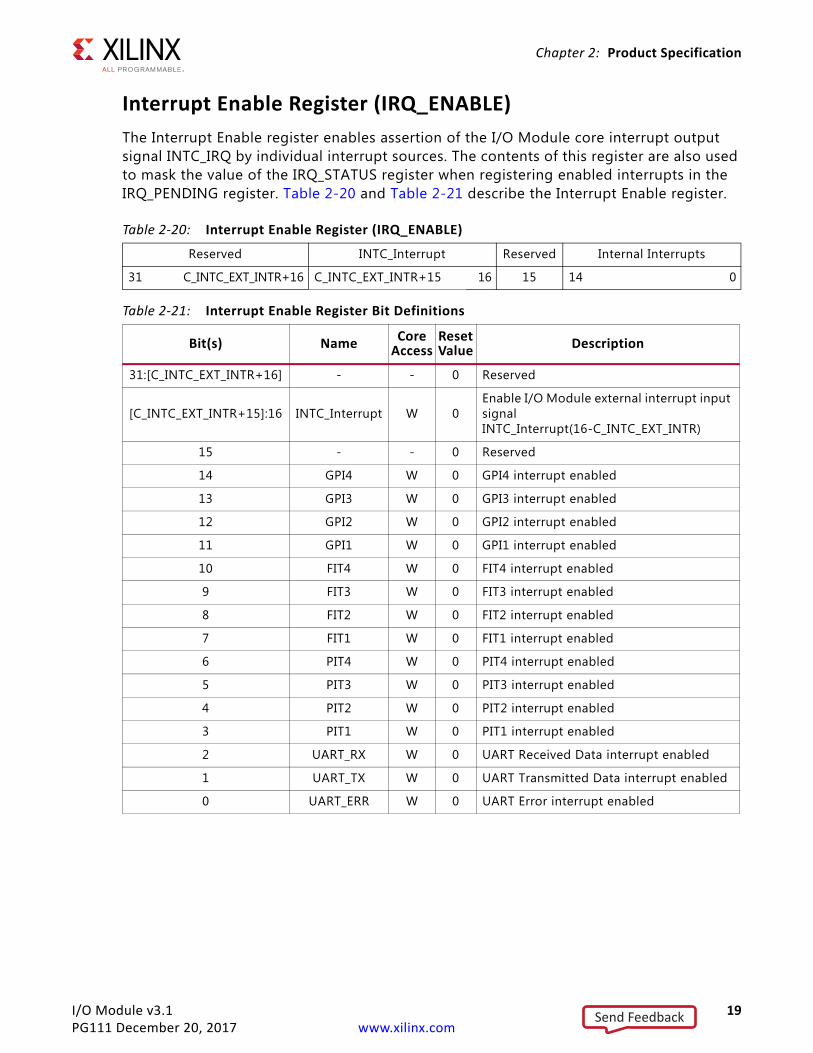
Interrupt Enable Register (IRQ_ENABLE)The Interrupt Enable register enables assertion of the I/O Module core interrupt output signal INTC_IRQ by individual interrupt sources. The contents of this register are also used to mask the value of the IRQ_STATUS register when registering enabled interrupts in the IRQ_PENDING register. Table 2-20 and Table 2-21 describe the Interrupt Enable register.
Table 2-20: Interrupt Enable Register (IRQ_ENABLE)
Reserved INTC_Interrupt Reserved Internal Interrupts
31 C_INTC_EXT_INTR+16 C_INTC_EXT_INTR+15 16 15 14 0
Table 2-21: Interrupt Enable Register Bit Definitions
Bit(s) Name CoreAccess
ResetValue Description
31:[C_INTC_EXT_INTR+16] - - 0 Reserved
[C_INTC_EXT_INTR+15]:16 INTC_Interrupt W 0Enable I/O Module external interrupt input signalINTC_Interrupt(16-C_INTC_EXT_INTR)
15 - - 0 Reserved
14 GPI4 W 0 GPI4 interrupt enabled
13 GPI3 W 0 GPI3 interrupt enabled
12 GPI2 W 0 GPI2 interrupt enabled
11 GPI1 W 0 GPI1 interrupt enabled
10 FIT4 W 0 FIT4 interrupt enabled
9 FIT3 W 0 FIT3 interrupt enabled
8 FIT2 W 0 FIT2 interrupt enabled
7 FIT1 W 0 FIT1 interrupt enabled
6 PIT4 W 0 PIT4 interrupt enabled
5 PIT3 W 0 PIT3 interrupt enabled
4 PIT2 W 0 PIT2 interrupt enabled
3 PIT1 W 0 PIT1 interrupt enabled
2 UART_RX W 0 UART Received Data interrupt enabled
1 UART_TX W 0 UART Transmitted Data interrupt enabled
0 UART_ERR W 0 UART Error interrupt enabled
Send Feedback
I/O Module v3.1 20PG111 December 20, 2017 www.xilinx.com
Chapter 2: Product Specification
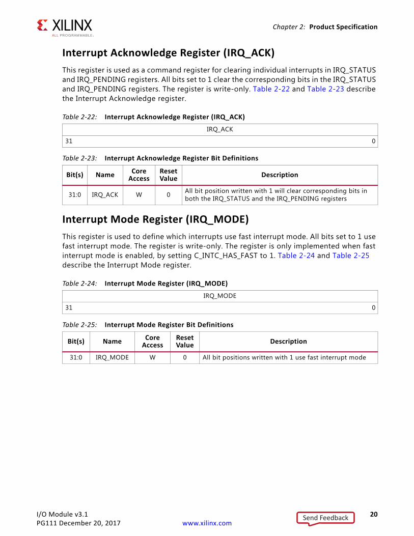
Interrupt Acknowledge Register (IRQ_ACK)This register is used as a command register for clearing individual interrupts in IRQ_STATUS and IRQ_PENDING registers. All bits set to 1 clear the corresponding bits in the IRQ_STATUS and IRQ_PENDING registers. The register is write-only. Table 2-22 and Table 2-23 describe the Interrupt Acknowledge register.
Interrupt Mode Register (IRQ_MODE)This register is used to define which interrupts use fast interrupt mode. All bits set to 1 use fast interrupt mode. The register is write-only. The register is only implemented when fast interrupt mode is enabled, by setting C_INTC_HAS_FAST to 1. Table 2-24 and Table 2-25 describe the Interrupt Mode register.
Table 2-22: Interrupt Acknowledge Register (IRQ_ACK)
IRQ_ACK
31 0
Table 2-23: Interrupt Acknowledge Register Bit Definitions
Bit(s) Name CoreAccess
ResetValue Description
31:0 IRQ_ACK W 0 All bit position written with 1 will clear corresponding bits in both the IRQ_STATUS and the IRQ_PENDING registers
Table 2-24: Interrupt Mode Register (IRQ_MODE)
IRQ_MODE
31 0
Table 2-25: Interrupt Mode Register Bit Definitions
Bit(s) Name CoreAccess
ResetValue Description
31:0 IRQ_MODE W 0 All bit positions written with 1 use fast interrupt mode
Send Feedback
I/O Module v3.1 21PG111 December 20, 2017 www.xilinx.com
Chapter 2: Product Specification
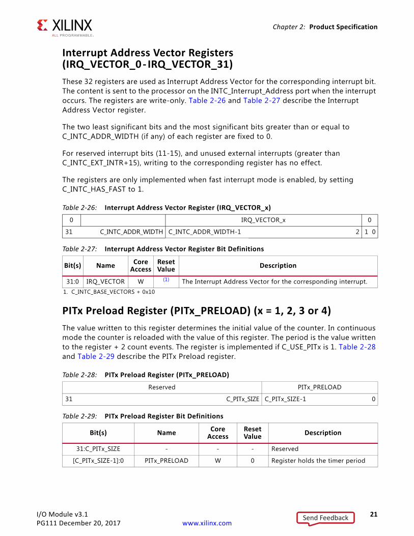
Interrupt Address Vector Registers (IRQ_VECTOR_0 - IRQ_VECTOR_31)These 32 registers are used as Interrupt Address Vector for the corresponding interrupt bit. The content is sent to the processor on the INTC_Interrupt_Address port when the interrupt occurs. The registers are write-only. Table 2-26 and Table 2-27 describe the Interrupt Address Vector register.
The two least significant bits and the most significant bits greater than or equal to C_INTC_ADDR_WIDTH (if any) of each register are fixed to 0.
For reserved interrupt bits (11-15), and unused external interrupts (greater than C_INTC_EXT_INTR+15), writing to the corresponding register has no effect.
The registers are only implemented when fast interrupt mode is enabled, by setting C_INTC_HAS_FAST to 1.
PITx Preload Register (PITx_PRELOAD) (x = 1, 2, 3 or 4)The value written to this register determines the initial value of the counter. In continuous mode the counter is reloaded with the value of this register. The period is the value written to the register + 2 count events. The register is implemented if C_USE_PITx is 1. Table 2-28 and Table 2-29 describe the PITx Preload register.
Table 2-26: Interrupt Address Vector Register (IRQ_VECTOR_x)
0 IRQ_VECTOR_x 0
31 C_INTC_ADDR_WIDTH C_INTC_ADDR_WIDTH-1 2 1 0
Table 2-27: Interrupt Address Vector Register Bit Definitions
Bit(s) Name CoreAccess
ResetValue Description
31:0 IRQ_VECTOR W (1) The Interrupt Address Vector for the corresponding interrupt.1. C_INTC_BASE_VECTORS + 0x10
Table 2-28: PITx Preload Register (PITx_PRELOAD)
Reserved PITx_PRELOAD
31 C_PITx_SIZE C_PITx_SIZE-1 0
Table 2-29: PITx Preload Register Bit Definitions
Bit(s) Name CoreAccess
ResetValue Description
31:C_PITx_SIZE - - - Reserved
[C_PITx_SIZE-1]:0 PITx_PRELOAD W 0 Register holds the timer period
Send Feedback
I/O Module v3.1 22PG111 December 20, 2017 www.xilinx.com
Chapter 2: Product Specification
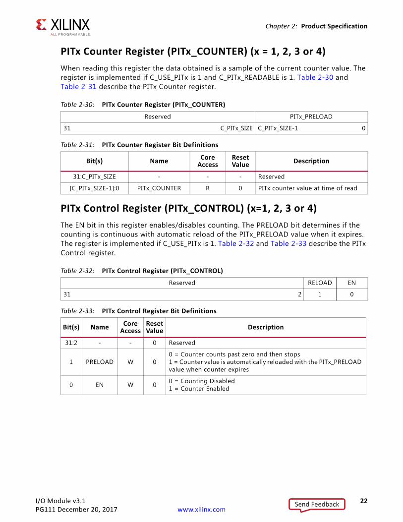
PITx Counter Register (PITx_COUNTER) (x = 1, 2, 3 or 4)When reading this register the data obtained is a sample of the current counter value. The register is implemented if C_USE_PITx is 1 and C_PITx_READABLE is 1. Table 2-30 and Table 2-31 describe the PITx Counter register.
PITx Control Register (PITx_CONTROL) (x=1, 2, 3 or 4)The EN bit in this register enables/disables counting. The PRELOAD bit determines if the counting is continuous with automatic reload of the PITx_PRELOAD value when it expires. The register is implemented if C_USE_PITx is 1. Table 2-32 and Table 2-33 describe the PITx Control register.
Table 2-30: PITx Counter Register (PITx_COUNTER)
Reserved PITx_PRELOAD
31 C_PITx_SIZE C_PITx_SIZE-1 0
Table 2-31: PITx Counter Register Bit Definitions
Bit(s) Name CoreAccess
ResetValue Description
31:C_PITx_SIZE - - - Reserved
[C_PITx_SIZE-1]:0 PITx_COUNTER R 0 PITx counter value at time of read
Table 2-32: PITx Control Register (PITx_CONTROL)
Reserved RELOAD EN
31 2 1 0
Table 2-33: PITx Control Register Bit Definitions
Bit(s) Name CoreAccess
ResetValue Description
31:2 - - 0 Reserved
1 PRELOAD W 00 = Counter counts past zero and then stops1 = Counter value is automatically reloaded with the PITx_PRELOAD value when counter expires
0 EN W 0 0 = Counting Disabled1 = Counter Enabled
Send Feedback
I/O Module v3.1 23PG111 December 20, 2017 www.xilinx.com
Chapter 3
Designing with the CoreThis chapter includes guidelines and additional information to facilitate designing with the core.
General Design Guidelines
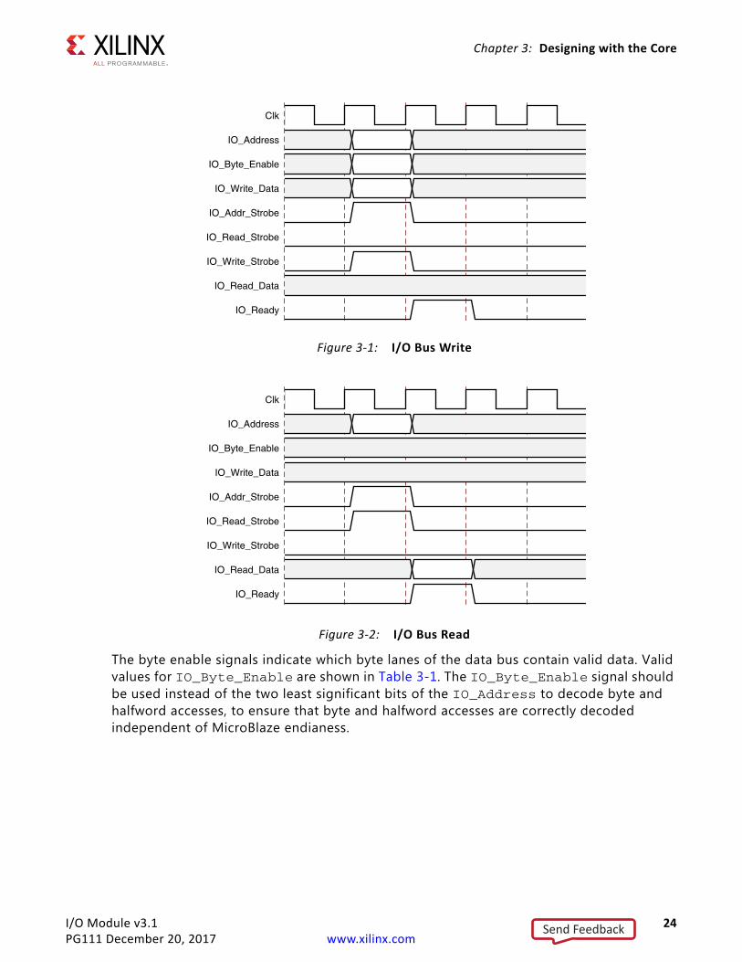
I/O BusThe I/O bus provides a simple bus for accessing to external modules using MicroBlaze™ Load/Store instructions. The I/O bus is mapped at address C_IO_BASEADDR–C_IO_HIGHADDR in the MicroBlaze memory space, with the I/O bus address directly reflecting the byte address used by MicroBlaze Load/Store instructions. I/O bus data is 32-bit wide, with byte enables to write byte and half-word data.
The I/O bus has a ready handshake to handle different waitstate needs, from IO_Ready asserted the cycle after the IO_Addr_Strobe is asserted to as many cycles as needed. There is no timeout on the I/O bus and MicroBlaze is stalled until IO_Ready is asserted. IO_Address, IO_Byte_Enable, IO_Write_Data, IO_Read_Strobe, IO_Write_Strobe are only valid when IO_Addr_Strobe is asserted. For read access IO_Read_Data is sampled at the rising Clk edge, when the slave has asserted IO_Ready.
I/O bus read and write transactions can be found in the two following timing diagrams in Figure 3-1 and Figure 3-2.
Send Feedback
I/O Module v3.1 24PG111 December 20, 2017 www.xilinx.com
Chapter 3: Designing with the Core
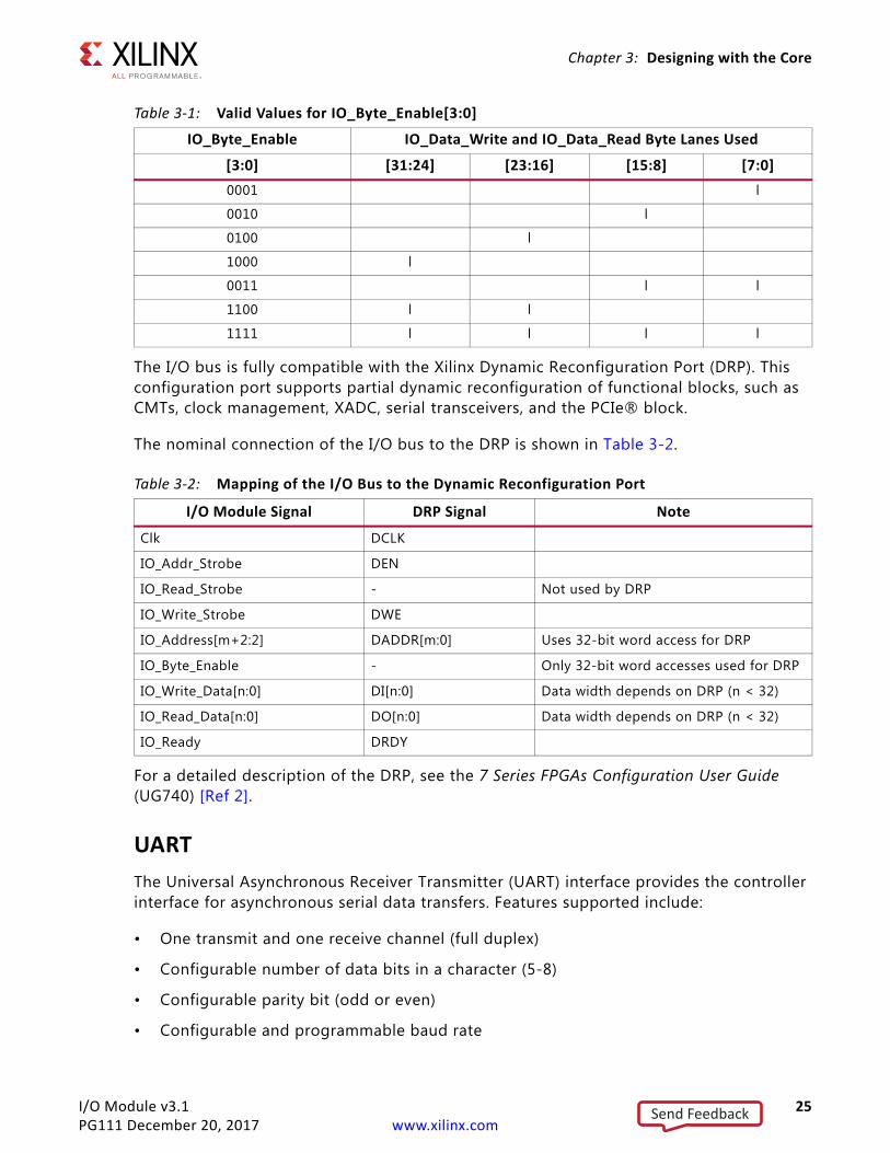
The byte enable signals indicate which byte lanes of the data bus contain valid data. Valid values for IO_Byte_Enable are shown in Table 3-1. The IO_Byte_Enable signal should be used instead of the two least significant bits of the IO_Address to decode byte and halfword accesses, to ensure that byte and halfword accesses are correctly decoded independent of MicroBlaze endianess.
X-Ref Target - Figure 3-1
Figure 3-1: I/O Bus WriteX-Ref Target - Figure 3-2
Figure 3-2: I/O Bus Read
Clk
IO_Address
IO_Byte_Enable
IO_Write_Data
IO_Addr_Strobe
IO_Read_Strobe
IO_Write_Strobe
IO_Read_Data
IO_Ready
Send Feedback
I/O Module v3.1 25PG111 December 20, 2017 www.xilinx.com
Chapter 3: Designing with the Core
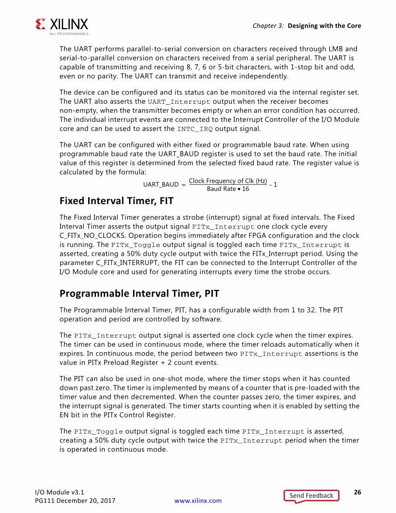
The I/O bus is fully compatible with the Xilinx Dynamic Reconfiguration Port (DRP). This configuration port supports partial dynamic reconfiguration of functional blocks, such as CMTs, clock management, XADC, serial transceivers, and the PCIe® block.
The nominal connection of the I/O bus to the DRP is shown in Table 3-2.
For a detailed description of the DRP, see the 7 Series FPGAs Configuration User Guide (UG740) [Ref 2].
UARTThe Universal Asynchronous Receiver Transmitter (UART) interface provides the controller interface for asynchronous serial data transfers. Features supported include:
• One transmit and one receive channel (full duplex)
• Configurable number of data bits in a character (5-8)
• Configurable parity bit (odd or even)
• Configurable and programmable baud rate
Table 3-1: Valid Values for IO_Byte_Enable[3:0]
IO_Byte_Enable IO_Data_Write and IO_Data_Read Byte Lanes Used
[3:0] [31:24] [23:16] [15:8] [7:0]0001 l
0010 l
0100 l
1000 l
0011 l l
1100 l l
1111 l l l l
Table 3-2: Mapping of the I/O Bus to the Dynamic Reconfiguration Port
I/O Module Signal DRP Signal Note
Clk DCLK
IO_Addr_Strobe DEN
IO_Read_Strobe - Not used by DRP
IO_Write_Strobe DWE
IO_Address[m+2:2] DADDR[m:0] Uses 32-bit word access for DRP
IO_Byte_Enable - Only 32-bit word accesses used for DRP
IO_Write_Data[n:0] DI[n:0] Data width depends on DRP (n < 32)
IO_Read_Data[n:0] DO[n:0] Data width depends on DRP (n < 32)
IO_Ready DRDY
Send Feedback
I/O Module v3.1 26PG111 December 20, 2017 www.xilinx.com
Chapter 3: Designing with the Core
The UART performs parallel-to-serial conversion on characters received through LMB and serial-to-parallel conversion on characters received from a serial peripheral. The UART is capable of transmitting and receiving 8, 7, 6 or 5-bit characters, with 1-stop bit and odd, even or no parity. The UART can transmit and receive independently.
The device can be configured and its status can be monitored via the internal register set. The UART also asserts the UART_Interrupt output when the receiver becomes non-empty, when the transmitter becomes empty or when an error condition has occurred. The individual interrupt events are connected to the Interrupt Controller of the I/O Module core and can be used to assert the INTC_IRQ output signal.
The UART can be configured with either fixed or programmable baud rate. When using programmable baud rate the UART_BAUD register is used to set the baud rate. The initial value of this register is determined from the selected fixed baud rate. The register value is calculated by the formula:
Fixed Interval Timer, FITThe Fixed Interval Timer generates a strobe (interrupt) signal at fixed intervals. The Fixed Interval Timer asserts the output signal FITx_Interrupt one clock cycle every C_FITx_NO_CLOCKS. Operation begins immediately after FPGA configuration and the clock is running. The FITx_Toggle output signal is toggled each time FITx_Interrupt is asserted, creating a 50% duty cycle output with twice the FITx_Interrupt period. Using the parameter C_FITx_INTERRUPT, the FIT can be connected to the Interrupt Controller of the I/O Module core and used for generating interrupts every time the strobe occurs.
Programmable Interval Timer, PITThe Programmable Interval Timer, PIT, has a configurable width from 1 to 32. The PIT operation and period are controlled by software.
The PITx_Interrupt output signal is asserted one clock cycle when the timer expires. The timer can be used in continuous mode, where the timer reloads automatically when it expires. In continuous mode, the period between two PITx_Interrupt assertions is the value in PITx Preload Register + 2 count events.
The PIT can also be used in one-shot mode, where the timer stops when it has counted down past zero. The timer is implemented by means of a counter that is pre-loaded with the timer value and then decremented. When the counter passes zero, the timer expires, and the interrupt signal is generated. The timer starts counting when it is enabled by setting the EN bit in the PITx Control Register.
The PITx_Toggle output signal is toggled each time PITx_Interrupt is asserted, creating a 50% duty cycle output with twice the PITx_Interrupt period when the timer is operated in continuous mode.
UART_BAUD Clock Frequency of Clk (Hz)Baud Rate 16•
------------------------------------------------------------ 1–=
Send Feedback
I/O Module v3.1 27PG111 December 20, 2017 www.xilinx.com
Chapter 3: Designing with the Core
The value of the counter that implements the timer can be read by software if the C_PITx_Readable parameter is enabled.The PIT can have a pre-scaler connected from any FITx, PITx, or External. The pre-scaler is selected by the C_PITx_PRESCALER parameter. The PIT has no pre-scaler by default. If External is selected the input signal PITx_Enable is used as pre-scaler. Selecting External as pre-scaler can also be used to measure the width in clock cycles of a signal connected to the PITx_Enable input.
Using the parameter C_PITx_INTERRUPT, the PIT can be connected to the Interrupt Controller of the I/O Module core and used for generating interrupts every time it expires.
General Purpose Output, GPOThe General Purpose Output, GPO, drives I/O Module GPO output signals defined by the value of the GPOx register, programmable from software. The width of the GPOx is defined by the C_GPOx_SIZE and the initial value is defined by the parameter C_GPOx_INIT. When the GPOx register is written, the value of the GPOx output signals change accordingly.
General Purpose Input, GPIThe General Purpose Input, GPI, makes it possible for software to sample the value of theI/O Module GPI input signals by reading the GPIx register. The width of GPIx is defined by the parameter C_GPIx_SIZE.
Using the parameter C_GPIx_INTERRUPT, the GPI can be connected to the Interrupt Controller of the I/O Module core and used for generating interrupts every time an input changes (both edges), every time it changes from 0 to 1 (rising edge), or every time it changes from 1 to 0 (falling edge).
Interrupt Controller INTCThe Interrupt Controller handles both I/O module internal interrupt events and external ones. The internal interrupt events originate from the UART, the Fixed Interval Timers, the Programmable Interval Timers, or the General Purpose Inputs. For an internal interrupt to be generated on the INTC_IRQ output, the corresponding I/O Module core parameter needs to be set, for example, C_UART_RX_INTERRUPT=1, and that particular interrupt needs to be enabled in the Interrupt Enable Register.
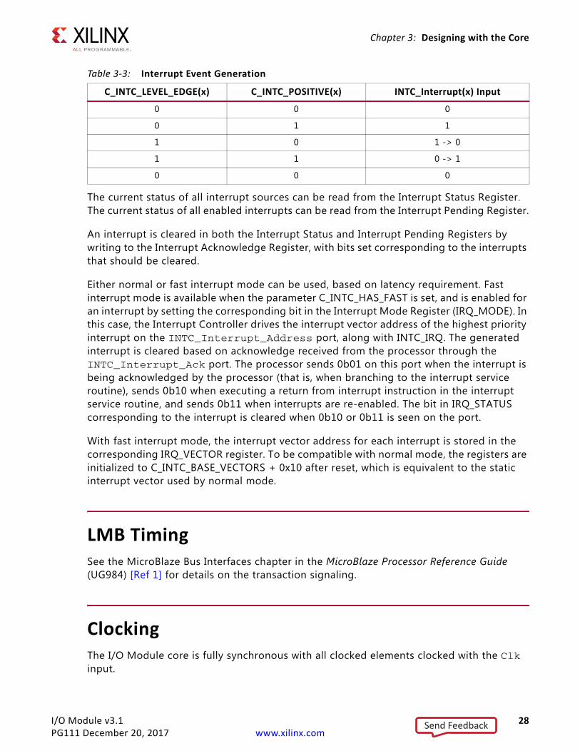
The Interrupt Controller supports up to 16 external interrupts using the INTC_Interrupt inputs. The number of external interrupts is defined by the parameter, C_INTC_INTR_SIZE. The external interrupt signals can be individually configured as either edge or level sensitive by the C_INTC_LEVEL_EDGE parameter. The polarity of the external interrupt signals can be individually configured to be either active-High (rising edge) or Low (falling edge) by the C_INTC_POSITIVE parameter. Interrupt events for external interrupt sources are generated according to Table 3-3.
Send Feedback
I/O Module v3.1 28PG111 December 20, 2017 www.xilinx.com
Chapter 3: Designing with the Core
The current status of all interrupt sources can be read from the Interrupt Status Register. The current status of all enabled interrupts can be read from the Interrupt Pending Register.
An interrupt is cleared in both the Interrupt Status and Interrupt Pending Registers by writing to the Interrupt Acknowledge Register, with bits set corresponding to the interrupts that should be cleared.
Either normal or fast interrupt mode can be used, based on latency requirement. Fast interrupt mode is available when the parameter C_INTC_HAS_FAST is set, and is enabled for an interrupt by setting the corresponding bit in the Interrupt Mode Register (IRQ_MODE). In this case, the Interrupt Controller drives the interrupt vector address of the highest priority interrupt on the INTC_Interrupt_Address port, along with INTC_IRQ. The generated interrupt is cleared based on acknowledge received from the processor through the INTC_Interrupt_Ack port. The processor sends 0b01 on this port when the interrupt is being acknowledged by the processor (that is, when branching to the interrupt service routine), sends 0b10 when executing a return from interrupt instruction in the interrupt service routine, and sends 0b11 when interrupts are re-enabled. The bit in IRQ_STATUS corresponding to the interrupt is cleared when 0b10 or 0b11 is seen on the port.
With fast interrupt mode, the interrupt vector address for each interrupt is stored in the corresponding IRQ_VECTOR register. To be compatible with normal mode, the registers are initialized to C_INTC_BASE_VECTORS + 0x10 after reset, which is equivalent to the static interrupt vector used by normal mode.
LMB TimingSee the MicroBlaze Bus Interfaces chapter in the MicroBlaze Processor Reference Guide (UG984) [Ref 1] for details on the transaction signaling.
ClockingThe I/O Module core is fully synchronous with all clocked elements clocked with the Clk input.
Table 3-3: Interrupt Event Generation
C_INTC_LEVEL_EDGE(x) C_INTC_POSITIVE(x) INTC_Interrupt(x) Input
0 0 0
0 1 1
1 0 1 -> 0
1 1 0 -> 1
0 0 0
Send Feedback
I/O Module v3.1 29PG111 December 20, 2017 www.xilinx.com
Chapter 3: Designing with the Core
ResetsThe Rst input is the master reset input signal for the I/O Module core.
When Triple Modular Redundancy is use the additional TMR_Rst input signal provides the option to only reset the flip-flops that are not majority voted, to support TMR recovery.
Protocol DescriptionSee the LMB Interface Description timing diagrams in the MicroBlaze Processor Reference Guide (UG984) [Ref 1].
Send Feedback
I/O Module v3.1 30PG111 December 20, 2017 www.xilinx.com
Chapter 4
Design Flow StepsThis chapter describes customizing and generating the core, constraining the core, and the simulation, synthesis and implementation steps that are specific to this IP core. More detailed information about the standard Vivado® design flows and the IP integrator can be found in the following Vivado Design Suite user guides:
• Vivado Design Suite User Guide: Designing IP Subsystems using IP Integrator (UG994) [Ref 4]
• Vivado Design Suite User Guide: Designing with IP (UG896) [Ref 5]
• Vivado Design Suite User Guide: Getting Started (UG910) [Ref 6]
• Vivado Design Suite User Guide: Logic Simulation (UG900) [Ref 7]
Customizing and Generating the CoreThis chapter includes information on using Xilinx tools to customize and generate the core in the Vivado Design Suite.
If you are customizing and generating the core in the Vivado IP integrator, see the Vivado Design Suite User Guide: Designing IP Subsystems using IP Integrator (UG994) [Ref 4] for detailed information. IP integrator might auto-compute certain configuration values when validating or generating the design. To check whether the values do change, see the description of the parameter in this chapter. To view the parameter value you can run the validate_bd_design command in the Tcl console.
You can customize the IP for use in your design by specifying values for the various parameters associated with the IP core using the following steps:
1. Select the IP from the IP catalog.
2. Double-click the selected IP or select the Customize IP command from the toolbar or right-click menu.
For details, see the Vivado Design Suite User Guide: Designing with IP (UG896) [Ref 5] and the Vivado Design Suite User Guide: Getting Started (UG910) [Ref 6].
Note: Figures in this chapter are illustrations of the Vivado IDE. This layout might vary from the current version.
Send Feedback
I/O Module v3.1 31PG111 December 20, 2017 www.xilinx.com
Chapter 4: Design Flow Steps
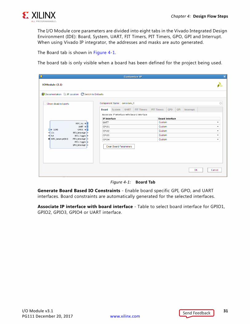
The I/O Module core parameters are divided into eight tabs in the Vivado Integrated Design Environment (IDE): Board, System, UART, FIT Timers, PIT Timers, GPO, GPI and Interrupt. When using Vivado IP integrator, the addresses and masks are auto generated.
The Board tab is shown in Figure 4-1.
The board tab is only visible when a board has been defined for the project being used.
Generate Board Based IO Constraints - Enable board specific GPI, GPO, and UART interfaces. Board constraints are automatically generated for the selected interfaces.
Associate IP interface with board interface - Table to select board interface for GPIO1, GPIO2, GPIO3, GPIO4 or UART interface.
X-Ref Target - Figure 4-1
Figure 4-1: Board Tab
Send Feedback
I/O Module v3.1 32PG111 December 20, 2017 www.xilinx.com
Chapter 4: Design Flow Steps
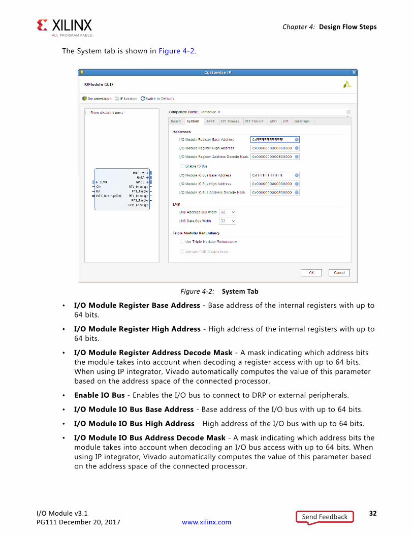
The System tab is shown in Figure 4-2.
• I/O Module Register Base Address - Base address of the internal registers with up to 64 bits.
• I/O Module Register High Address - High address of the internal registers with up to 64 bits.
• I/O Module Register Address Decode Mask - A mask indicating which address bits the module takes into account when decoding a register access with up to 64 bits. When using IP integrator, Vivado automatically computes the value of this parameter based on the address space of the connected processor.
• Enable IO Bus - Enables the I/O bus to connect to DRP or external peripherals.
• I/O Module IO Bus Base Address - Base address of the I/O bus with up to 64 bits.
• I/O Module IO Bus High Address - High address of the I/O bus with up to 64 bits.
• I/O Module IO Bus Address Decode Mask - A mask indicating which address bits the module takes into account when decoding an I/O bus access with up to 64 bits. When using IP integrator, Vivado automatically computes the value of this parameter based on the address space of the connected processor.
X-Ref Target - Figure 4-2
Figure 4-2: System Tab
Send Feedback
I/O Module v3.1 33PG111 December 20, 2017 www.xilinx.com
Chapter 4: Design Flow Steps
• Use Triple Modular Redundancy - Enable support for use in a Triple Modular Redundant (TMR) subsystem. When this parameter is set, the internal state is voted between this core and the two other cores in the subsystem, to ensure that single errors are corrected.
• Activate TMR Disable Input - Activate TMR disable functionality. When activated and the TMR_Disable input is set to one, the inputs from other I/O Modules are disregarded.
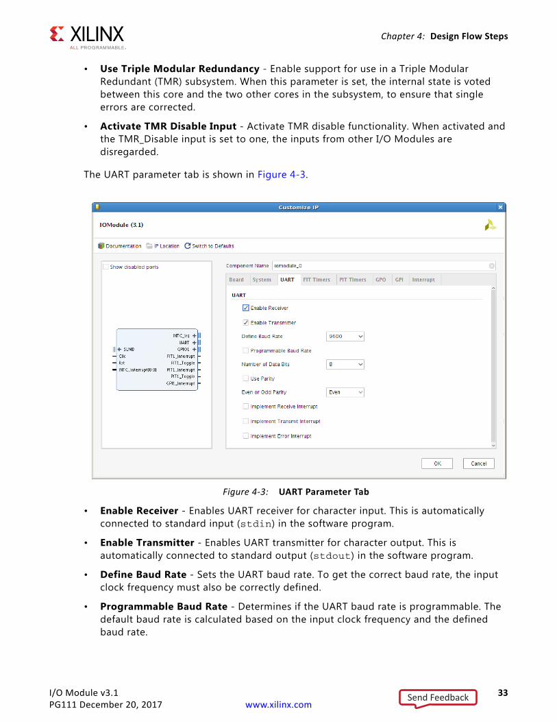
The UART parameter tab is shown in Figure 4-3.
• Enable Receiver - Enables UART receiver for character input. This is automatically connected to standard input (stdin) in the software program.
• Enable Transmitter - Enables UART transmitter for character output. This is automatically connected to standard output (stdout) in the software program.
• Define Baud Rate - Sets the UART baud rate. To get the correct baud rate, the input clock frequency must also be correctly defined.
• Programmable Baud Rate - Determines if the UART baud rate is programmable. The default baud rate is calculated based on the input clock frequency and the defined baud rate.
X-Ref Target - Figure 4-3
Figure 4-3: UART Parameter Tab
Send Feedback
I/O Module v3.1 34PG111 December 20, 2017 www.xilinx.com
Chapter 4: Design Flow Steps
• Number of Data Bits - Defines the number of data bits used by the UART. Should almost always be set to 8.
• Use Parity - Enable this parameter to use parity checking of the UART characters.
• Even or Odd Parity - Select odd or even parity. Only available when parity is used.
• Implement Receive Interrupt - Generate an interrupt when the UART has received a character. When the interrupt is not enabled the UART must be polled to check if data has been received.
• Implement Transmit Interrupt - Generate an interrupt when the UART has sent a character. When the interrupt is not enabled the UART must be polled to wait until data has been transmitted.
• Implement Error Interrupt - Generate an interrupt if an error occurs when the UART receives a character. This error can be a framing error, an overrun error or a parity error (if parity is used), When the interrupt is not enabled the UART must be polled to check if an error has occurred after a character has been received.
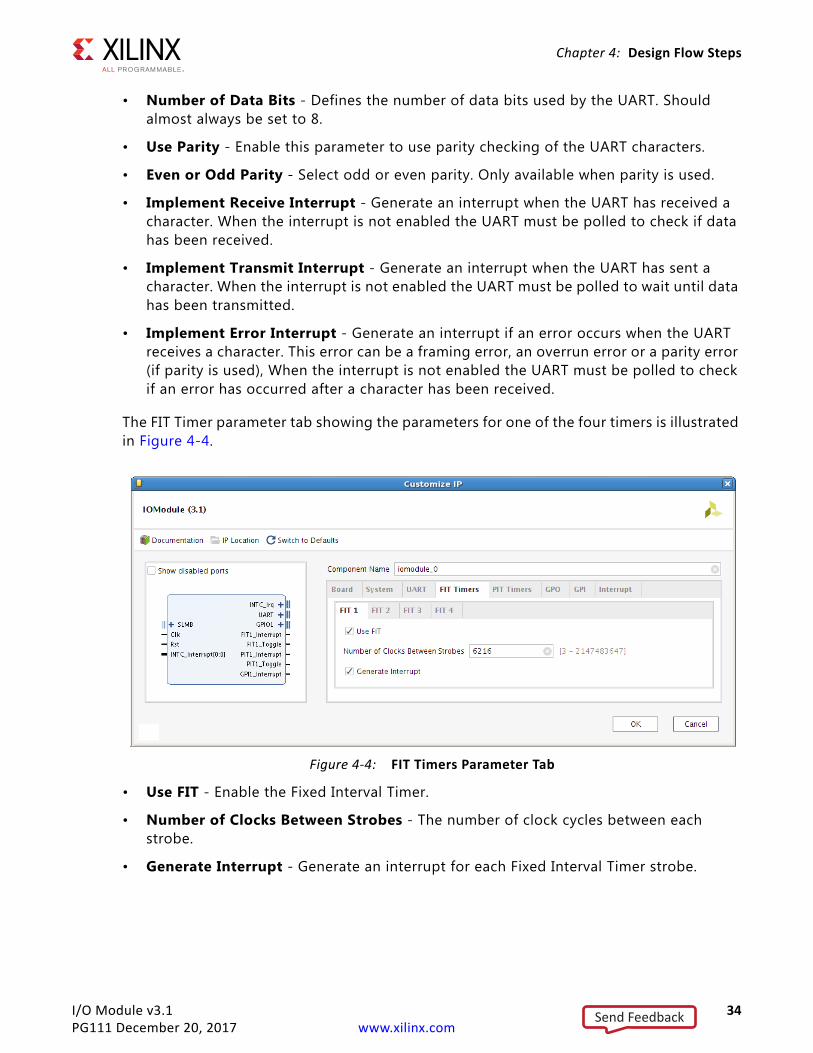
The FIT Timer parameter tab showing the parameters for one of the four timers is illustrated in Figure 4-4.
• Use FIT - Enable the Fixed Interval Timer.
• Number of Clocks Between Strobes - The number of clock cycles between each strobe.
• Generate Interrupt - Generate an interrupt for each Fixed Interval Timer strobe.
X-Ref Target - Figure 4-4
Figure 4-4: FIT Timers Parameter Tab
Send Feedback
I/O Module v3.1 35PG111 December 20, 2017 www.xilinx.com
Chapter 4: Design Flow Steps
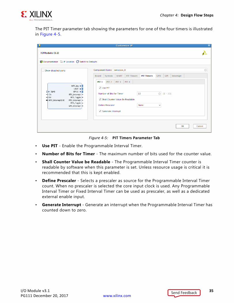
The PIT Timer parameter tab showing the parameters for one of the four timers is illustrated in Figure 4-5.
• Use PIT - Enable the Programmable Interval Timer.
• Number of Bits for Timer - The maximum number of bits used for the counter value.
• Shall Counter Value be Readable - The Programmable Interval Timer counter is readable by software when this parameter is set. Unless resource usage is critical it is recommended that this is kept enabled.
• Define Prescaler - Selects a prescaler as source for the Programmable Interval Timer count. When no prescaler is selected the core input clock is used. Any Programmable Interval Timer or Fixed Interval Timer can be used as prescaler, as well as a dedicated external enable input.
• Generate Interrupt - Generate an interrupt when the Programmable Interval Timer has counted down to zero.
X-Ref Target - Figure 4-5
Figure 4-5: PIT Timers Parameter Tab
Send Feedback
I/O Module v3.1 36PG111 December 20, 2017 www.xilinx.com
Chapter 4: Design Flow Steps
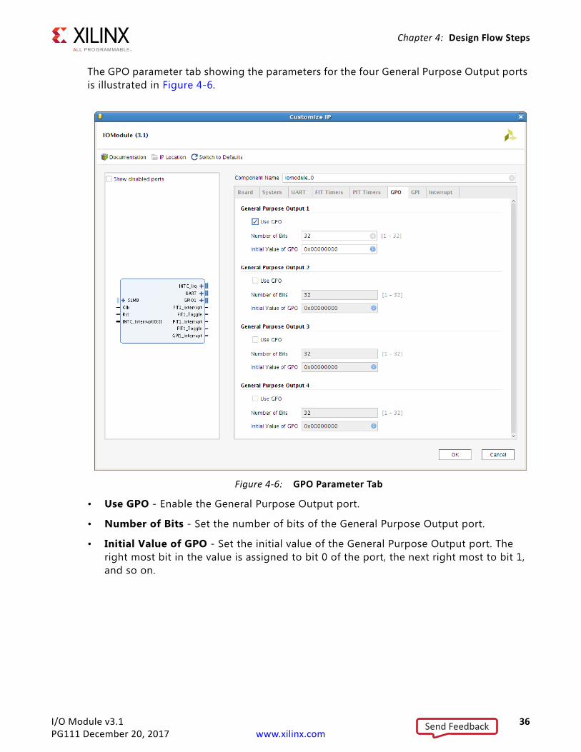
The GPO parameter tab showing the parameters for the four General Purpose Output ports is illustrated in Figure 4-6.
• Use GPO - Enable the General Purpose Output port.
• Number of Bits - Set the number of bits of the General Purpose Output port.
• Initial Value of GPO - Set the initial value of the General Purpose Output port. The right most bit in the value is assigned to bit 0 of the port, the next right most to bit 1, and so on.
X-Ref Target - Figure 4-6
Figure 4-6: GPO Parameter Tab
Send Feedback
I/O Module v3.1 37PG111 December 20, 2017 www.xilinx.com
Chapter 4: Design Flow Steps
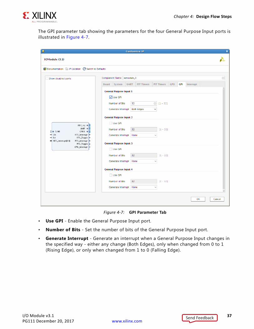
The GPI parameter tab showing the parameters for the four General Purpose Input ports is illustrated in Figure 4-7.
• Use GPI - Enable the General Purpose Input port.
• Number of Bits - Set the number of bits of the General Purpose Input port.
• Generate Interrupt - Generate an interrupt when a General Purpose Input changes in the specified way - either any change (Both Edges), only when changed from 0 to 1 (Rising Edge), or only when changed from 1 to 0 (Falling Edge).
X-Ref Target - Figure 4-7
Figure 4-7: GPI Parameter Tab
Send Feedback
I/O Module v3.1 38PG111 December 20, 2017 www.xilinx.com
Chapter 4: Design Flow Steps
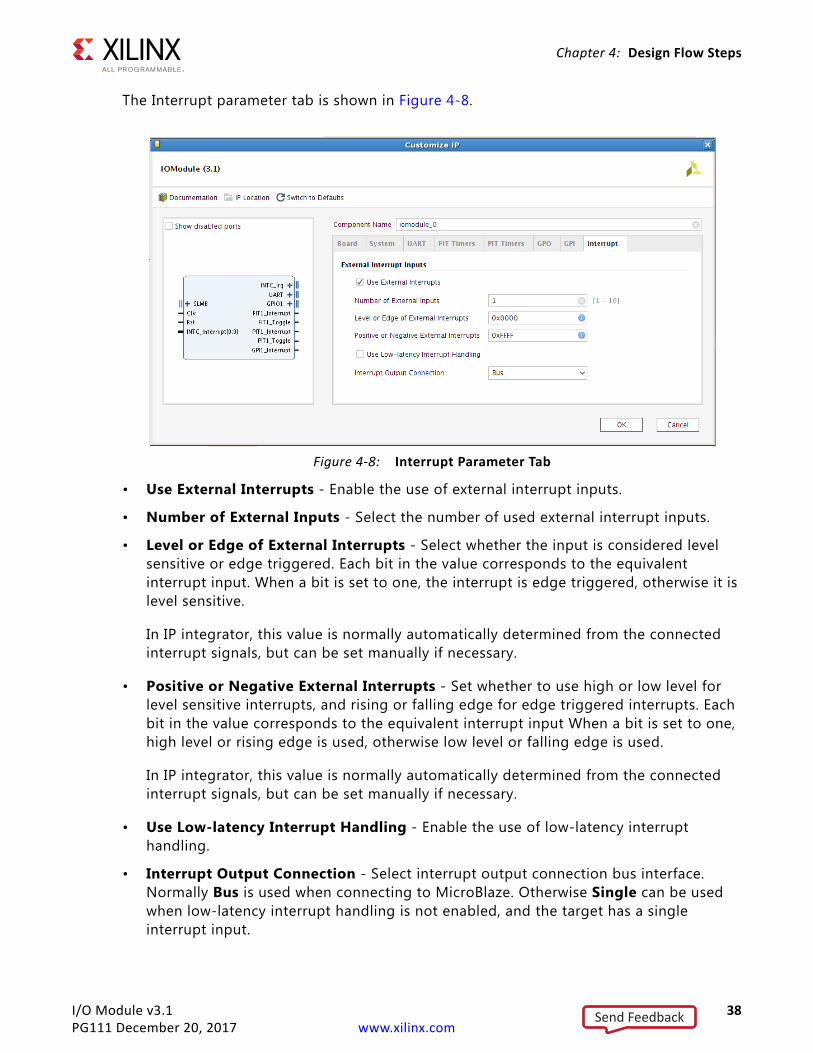
The Interrupt parameter tab is shown in Figure 4-8.
• Use External Interrupts - Enable the use of external interrupt inputs.
• Number of External Inputs - Select the number of used external interrupt inputs.
• Level or Edge of External Interrupts - Select whether the input is considered level sensitive or edge triggered. Each bit in the value corresponds to the equivalent interrupt input. When a bit is set to one, the interrupt is edge triggered, otherwise it is level sensitive.
In IP integrator, this value is normally automatically determined from the connected interrupt signals, but can be set manually if necessary.
• Positive or Negative External Interrupts - Set whether to use high or low level for level sensitive interrupts, and rising or falling edge for edge triggered interrupts. Each bit in the value corresponds to the equivalent interrupt input When a bit is set to one, high level or rising edge is used, otherwise low level or falling edge is used.
In IP integrator, this value is normally automatically determined from the connected interrupt signals, but can be set manually if necessary.
• Use Low-latency Interrupt Handling - Enable the use of low-latency interrupt handling.
• Interrupt Output Connection - Select interrupt output connection bus interface. Normally Bus is used when connecting to MicroBlaze. Otherwise Single can be used when low-latency interrupt handling is not enabled, and the target has a single interrupt input.
X-Ref Target - Figure 4-8
Figure 4-8: Interrupt Parameter Tab
Send Feedback
I/O Module v3.1 39PG111 December 20, 2017 www.xilinx.com
Chapter 4: Design Flow Steps
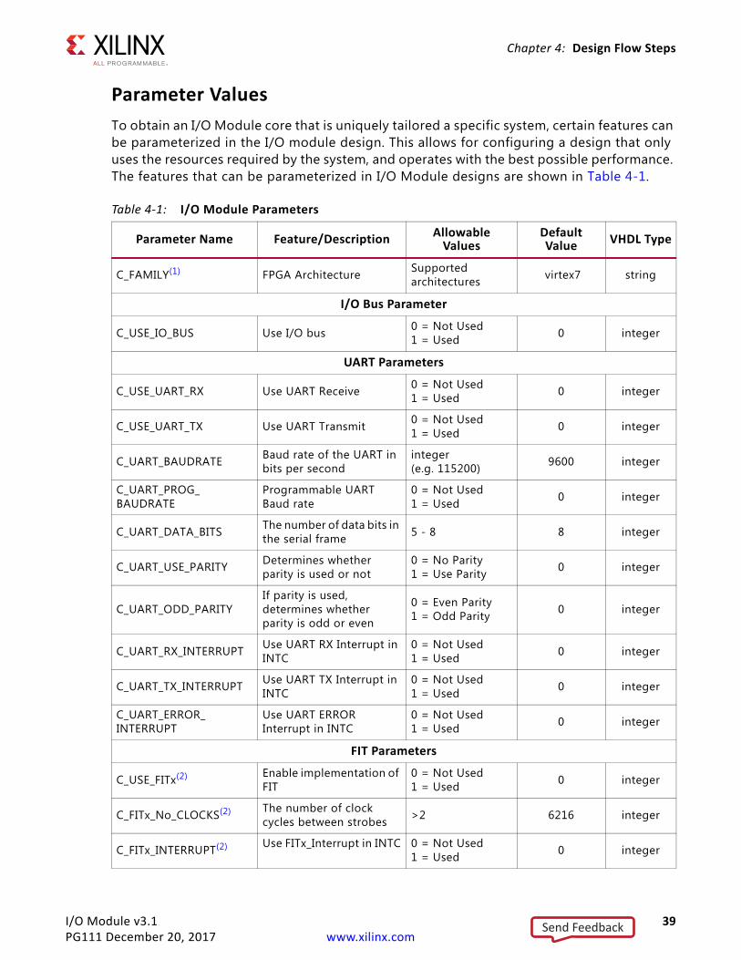
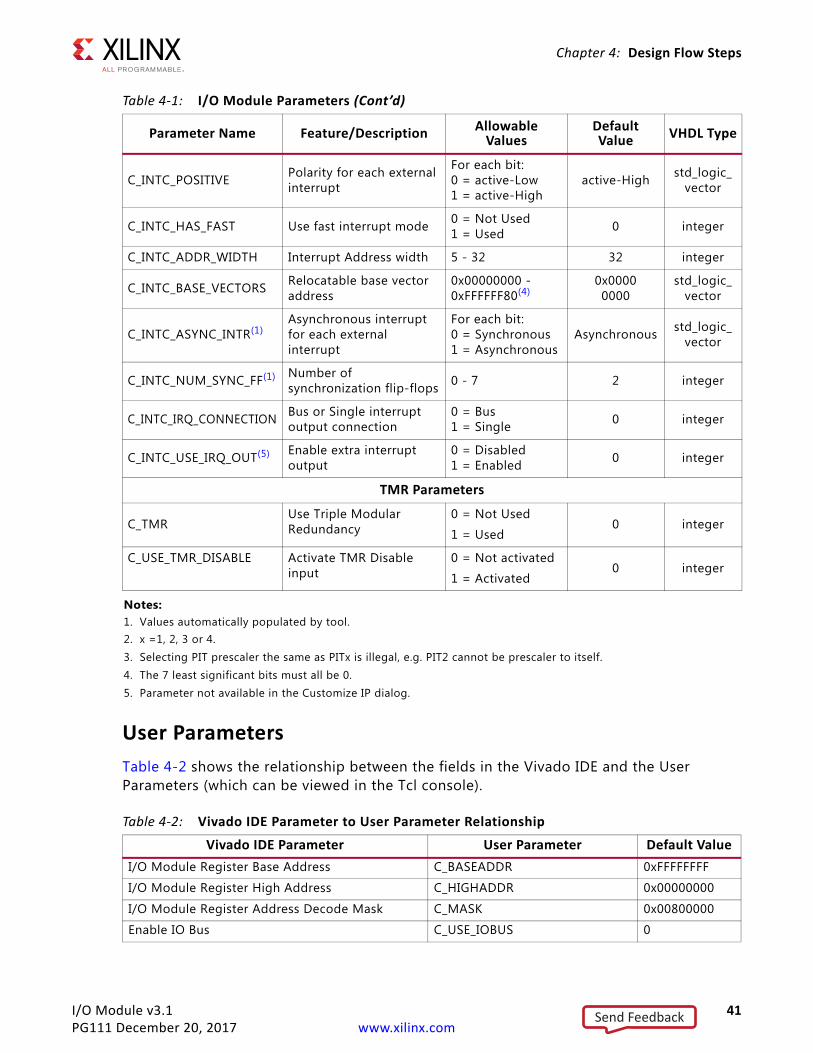
Parameter ValuesTo obtain an I/O Module core that is uniquely tailored a specific system, certain features can be parameterized in the I/O module design. This allows for configuring a design that only uses the resources required by the system, and operates with the best possible performance. The features that can be parameterized in I/O Module designs are shown in Table 4-1.
Table 4-1: I/O Module Parameters
Parameter Name Feature/Description AllowableValues
DefaultValue VHDL Type
C_FAMILY(1) FPGA Architecture Supportedarchitectures virtex7 string
I/O Bus Parameter
C_USE_IO_BUS Use I/O bus 0 = Not Used1 = Used 0 integer
UART Parameters
C_USE_UART_RX Use UART Receive 0 = Not Used1 = Used 0 integer
C_USE_UART_TX Use UART Transmit 0 = Not Used1 = Used 0 integer
C_UART_BAUDRATE Baud rate of the UART in bits per second
integer(e.g. 115200) 9600 integer
C_UART_PROG_BAUDRATE
Programmable UART Baud rate
0 = Not Used1 = Used 0 integer
C_UART_DATA_BITS The number of data bits in the serial frame 5 - 8 8 integer
C_UART_USE_PARITY Determines whether parity is used or not
0 = No Parity1 = Use Parity 0 integer
C_UART_ODD_PARITYIf parity is used, determines whether parity is odd or even
0 = Even Parity1 = Odd Parity 0 integer
C_UART_RX_INTERRUPT Use UART RX Interrupt in INTC
0 = Not Used1 = Used 0 integer
C_UART_TX_INTERRUPT Use UART TX Interrupt in INTC
0 = Not Used1 = Used 0 integer
C_UART_ERROR_INTERRUPT
Use UART ERROR Interrupt in INTC
0 = Not Used1 = Used 0 integer
FIT Parameters
C_USE_FITx(2) Enable implementation of FIT
0 = Not Used1 = Used 0 integer
C_FITx_No_CLOCKS(2) The number of clock cycles between strobes >2 6216 integer
C_FITx_INTERRUPT(2) Use FITx_Interrupt in INTC 0 = Not Used1 = Used 0 integer
Send Feedback
I/O Module v3.1 40PG111 December 20, 2017 www.xilinx.com
Chapter 4: Design Flow Steps
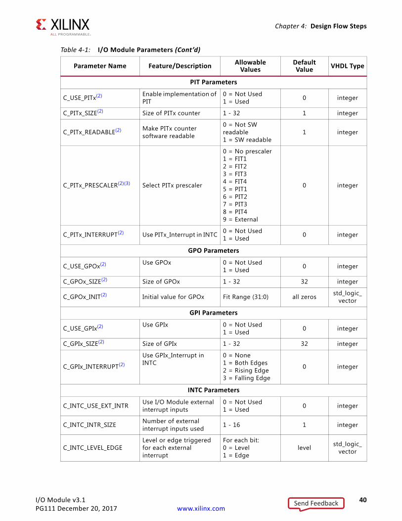
PIT Parameters
C_USE_PITx(2) Enable implementation of PIT
0 = Not Used1 = Used 0 integer
C_PITx_SIZE(2) Size of PITx counter 1 - 32 1 integer
C_PITx_READABLE(2) Make PITx counter software readable
0 = Not SWreadable1 = SW readable
1 integer
C_PITx_PRESCALER(2)(3) Select PITx prescaler
0 = No prescaler1 = FIT12 = FIT23 = FIT34 = FIT45 = PIT16 = PIT27 = PIT38 = PIT49 = External
0 integer
C_PITx_INTERRUPT(2) Use PITx_Interrupt in INTC 0 = Not Used1 = Used 0 integer
GPO Parameters
C_USE_GPOx(2) Use GPOx 0 = Not Used1 = Used 0 integer
C_GPOx_SIZE(2) Size of GPOx 1 - 32 32 integer
C_GPOx_INIT(2) Initial value for GPOx Fit Range (31:0) all zeros std_logic_vector
GPI Parameters
C_USE_GPIx(2) Use GPIx 0 = Not Used1 = Used 0 integer
C_GPIx_SIZE(2) Size of GPIx 1 - 32 32 integer
C_GPIx_INTERRUPT(2)
Use GPIx_Interrupt in INTC
0 = None1 = Both Edges2 = Rising Edge3 = Falling Edge
0 integer
INTC Parameters
C_INTC_USE_EXT_INTR Use I/O Module external interrupt inputs
0 = Not Used1 = Used 0 integer
C_INTC_INTR_SIZE Number of external interrupt inputs used 1 - 16 1 integer
C_INTC_LEVEL_EDGELevel or edge triggered for each external interrupt
For each bit:0 = Level1 = Edge
level std_logic_vector
Table 4-1: I/O Module Parameters (Cont’d)
Parameter Name Feature/Description AllowableValues
DefaultValue VHDL Type
Send Feedback
I/O Module v3.1 41PG111 December 20, 2017 www.xilinx.com
Chapter 4: Design Flow Steps
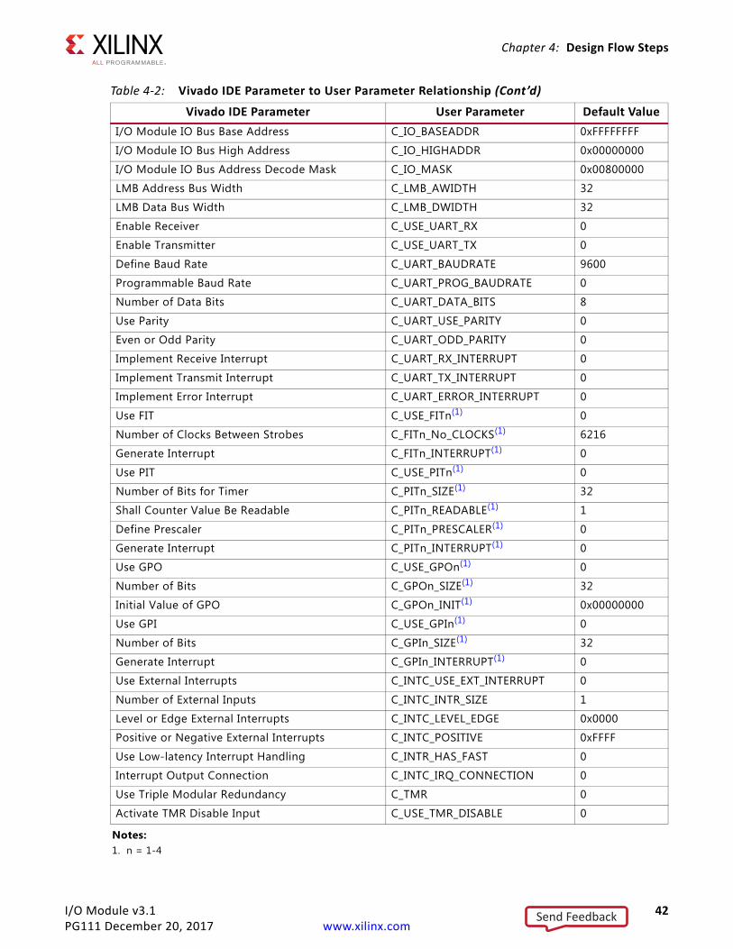
User ParametersTable 4-2 shows the relationship between the fields in the Vivado IDE and the User Parameters (which can be viewed in the Tcl console).
C_INTC_POSITIVE Polarity for each external interrupt
For each bit:0 = active-Low1 = active-High
active-High std_logic_vector
C_INTC_HAS_FAST Use fast interrupt mode 0 = Not Used1 = Used 0 integer
C_INTC_ADDR_WIDTH Interrupt Address width 5 - 32 32 integer
C_INTC_BASE_VECTORS Relocatable base vector address
0x00000000 -0xFFFFFF80(4)
0x00000000
std_logic_vector
C_INTC_ASYNC_INTR(1)Asynchronous interrupt for each external interrupt
For each bit:0 = Synchronous1 = Asynchronous
Asynchronous std_logic_vector
C_INTC_NUM_SYNC_FF(1) Number of synchronization flip-flops 0 - 7 2 integer
C_INTC_IRQ_CONNECTION Bus or Single interrupt output connection
0 = Bus1 = Single 0 integer
C_INTC_USE_IRQ_OUT(5) Enable extra interrupt output
0 = Disabled1 = Enabled 0 integer
TMR Parameters
C_TMRUse Triple Modular Redundancy
0 = Not Used
1 = Used0 integer
C_USE_TMR_DISABLE Activate TMR Disable input
0 = Not activated
1 = Activated0 integer
Notes: 1. Values automatically populated by tool.2. x =1, 2, 3 or 4.3. Selecting PIT prescaler the same as PITx is illegal, e.g. PIT2 cannot be prescaler to itself.4. The 7 least significant bits must all be 0.5. Parameter not available in the Customize IP dialog.
Table 4-2: Vivado IDE Parameter to User Parameter RelationshipVivado IDE Parameter User Parameter Default Value
I/O Module Register Base Address C_BASEADDR 0xFFFFFFFF
I/O Module Register High Address C_HIGHADDR 0x00000000
I/O Module Register Address Decode Mask C_MASK 0x00800000
Enable IO Bus C_USE_IOBUS 0
Table 4-1: I/O Module Parameters (Cont’d)
Parameter Name Feature/Description AllowableValues
DefaultValue VHDL Type
Send Feedback
I/O Module v3.1 42PG111 December 20, 2017 www.xilinx.com
Chapter 4: Design Flow Steps
I/O Module IO Bus Base Address C_IO_BASEADDR 0xFFFFFFFF
I/O Module IO Bus High Address C_IO_HIGHADDR 0x00000000
I/O Module IO Bus Address Decode Mask C_IO_MASK 0x00800000
LMB Address Bus Width C_LMB_AWIDTH 32
LMB Data Bus Width C_LMB_DWIDTH 32
Enable Receiver C_USE_UART_RX 0
Enable Transmitter C_USE_UART_TX 0
Define Baud Rate C_UART_BAUDRATE 9600
Programmable Baud Rate C_UART_PROG_BAUDRATE 0
Number of Data Bits C_UART_DATA_BITS 8
Use Parity C_UART_USE_PARITY 0
Even or Odd Parity C_UART_ODD_PARITY 0
Implement Receive Interrupt C_UART_RX_INTERRUPT 0
Implement Transmit Interrupt C_UART_TX_INTERRUPT 0
Implement Error Interrupt C_UART_ERROR_INTERRUPT 0
Use FIT C_USE_FITn(1) 0
Number of Clocks Between Strobes C_FITn_No_CLOCKS(1) 6216
Generate Interrupt C_FITn_INTERRUPT(1) 0
Use PIT C_USE_PITn(1) 0
Number of Bits for Timer C_PITn_SIZE(1) 32
Shall Counter Value Be Readable C_PITn_READABLE(1) 1
Define Prescaler C_PITn_PRESCALER(1) 0
Generate Interrupt C_PITn_INTERRUPT(1) 0
Use GPO C_USE_GPOn(1) 0
Number of Bits C_GPOn_SIZE(1) 32
Initial Value of GPO C_GPOn_INIT(1) 0x00000000
Use GPI C_USE_GPIn(1) 0
Number of Bits C_GPIn_SIZE(1) 32
Generate Interrupt C_GPIn_INTERRUPT(1) 0
Use External Interrupts C_INTC_USE_EXT_INTERRUPT 0
Number of External Inputs C_INTC_INTR_SIZE 1
Level or Edge External Interrupts C_INTC_LEVEL_EDGE 0x0000
Positive or Negative External Interrupts C_INTC_POSITIVE 0xFFFF
Use Low-latency Interrupt Handling C_INTR_HAS_FAST 0
Interrupt Output Connection C_INTC_IRQ_CONNECTION 0
Use Triple Modular Redundancy C_TMR 0
Activate TMR Disable Input C_USE_TMR_DISABLE 0
Notes: 1. n = 1-4
Table 4-2: Vivado IDE Parameter to User Parameter Relationship (Cont’d)
Vivado IDE Parameter User Parameter Default Value
Send Feedback
I/O Module v3.1 43PG111 December 20, 2017 www.xilinx.com
Chapter 4: Design Flow Steps
Output GenerationFor details, see the Vivado Design Suite User Guide: Designing with IP (UG896) [Ref 5].
Constraining the CoreThis section contains information about constraining the core in the Vivado Design Suite.
Required ConstraintsThis section is not applicable for this IP core.
Device, Package, and Speed Grade SelectionsThis section is not applicable for this IP core.
Clock FrequenciesThis section is not applicable for this IP core.
Clock ManagementThe I/O Module core is fully synchronous with all clocked elements clocked by the Clk input.
To operate properly when connected to MicroBlaze™, the Clk must be the same as the MicroBlaze Clk.
Clock PlacementThis section is not applicable for this IP core.
BankingThis section is not applicable for this IP core.
Transceiver PlacementThis section is not applicable for this IP core.
Send Feedback
I/O Module v3.1 44PG111 December 20, 2017 www.xilinx.com
Chapter 4: Design Flow Steps
I/O Standard and PlacementThis section is not applicable for this IP core.
SimulationFor comprehensive information about Vivado® simulation components, as well as information about using supported third party tools, see the Vivado Design Suite User Guide: Logic Simulation (UG900) [Ref 7].
IMPORTANT: For cores targeting 7 series or Zynq-7000 devices, UNIFAST libraries are not supported. Xilinx IP is tested and qualified with UNISIM libraries only.
Synthesis and ImplementationFor details about synthesis and implementation, see the Vivado Design Suite User Guide: Designing with IP (UG896) [Ref 5].
Send Feedback
I/O Module v3.1 45PG111 December 20, 2017 www.xilinx.com
Appendix A
UpgradingFor information on migrating from Xilinx ISE® Design Suite tools to the Vivado® Design Suite, see the ISE to Vivado Design Suite Migration Guide (UG911) [Ref 8].
UpgradeThis section describes changes that occur when upgrading from the previous version of the core.
The parameters, USE_BOARD_FLOW, GPIO1_BOARD_INTERFACE, GPIO1_BOARD_INTERFACE, GPIO1_BOARD_INTERFACE, GPIO1_BOARD_INTERFACE, and UART_BOARD_INTERFACE have been added in v2.1 of the core, to add support for board level constraints.
The parameters C_INTC_USE_IRQ_OUT and C_INTC_IRQ_CONNECTION have been added in v3.0 of the core, to provide additional interrupt output connection options.
The extra interrupt output port INTC_IRQ_OUT has been added in v3.0 of the core.
The parameters C_TMR and C_USE_TMR_DISABLE have been added in v3.1 of the core, to support Triple Modular Redundancy.
The additional ports FromAVote, FromBVote, TMR_Disable, TMR_Rst, and ToVote have been added in v3.1 of the core, to support Triple Modular Redundancy.
Send Feedback
I/O Module v3.1 46PG111 December 20, 2017 www.xilinx.com
Appendix B
DebuggingThis appendix includes details about resources available on the Xilinx Support website and debugging tools.
Finding Help on Xilinx.comTo help in the design and debug process when using the I/O Module, the Xilinx Support web page contains key resources such as product documentation, release notes, answer records, information about known issues, and links for obtaining further product support.
DocumentationThis product guide is the main document associated with the I/O Module. This guide, along with documentation related to all products that aid in the design process, can be found on the Xilinx Support web page or by using the Xilinx® Documentation Navigator.
Download the Xilinx Documentation Navigator from the Downloads page. For more information about this tool and the features available, open the online help after installation.
Answer RecordsAnswer Records include information about commonly encountered problems, helpful information on how to resolve these problems, and any known issues with a Xilinx product. Answer Records are created and maintained daily ensuring that users have access to the most accurate information available.
Answer Records for this core can be located by using the Search Support box on the main Xilinx support web page. To maximize your search results, use proper keywords such as
• Product name
• Tool message(s)
• Summary of the issue encountered
A filter search is available after results are returned to further target the results.
Send Feedback

I/O Module v3.1 47PG111 December 20, 2017 www.xilinx.com
Appendix B: Debugging
Master Answer Record for the I/O Module Core
AR: 54445
Technical SupportXilinx provides technical support at the Xilinx Support web page for this LogiCORE™ IP product when used as described in the product documentation. Xilinx cannot guarantee timing, functionality, or support if you do any of the following:
• Implement the solution in devices that are not defined in the documentation.
• Customize the solution beyond that allowed in the product documentation.
• Change any section of the design labeled DO NOT MODIFY.
To contact Xilinx Technical Support, navigate to the Xilinx Support web page.
Debug ToolsThe main tool available to address I/O Module design issues is the Vivado® Design Suite debug feature.
Vivado Design Suite Debug FeatureThe Vivado® Design Suite debug feature inserts logic analyzer and virtual I/O cores directly into your design. The debug feature also allows you to set trigger conditions to capture application and integrated block port signals in hardware. Captured signals can then be analyzed. This feature in the Vivado IDE is used for logic debugging and validation of a design running in Xilinx devices.
The Vivado logic analyzer is used to interact with the logic debug IP cores, including:
• ILA 2.0 (and later versions)
• VIO 2.0 (and later versions)
See the Vivado Design Suite User Guide: Programming and Debugging (UG908) [Ref 9].
Reference BoardsAll 7 series Xilinx development boards support the I/O Module core. These boards can be used to prototype designs and establish that the core can communicate with the system.
Send Feedback
I/O Module v3.1 48PG111 December 20, 2017 www.xilinx.com
Appendix B: Debugging
Simulation DebugThe simulation debug flow for Mentor Graphics Questa Simulator (QuestaSim) is described below. A similar approach can be used with other simulators.
• Check for the latest supported versions of QuestaSim in the Xilinx Design Tools: Release Notes Guide. Is this version being used? If not, update to this version.
• If using Verilog, do you have a mixed mode simulation license? If not, obtain a mixed-mode license.
• Ensure that the proper libraries are compiled and mapped. In the Vivado Design Suite Flow > Simulation Settings can be used to define the libraries.
• Have you associated the intended software program for the MicroBlaze processor with the simulation? Use the command Tools > Associate ELF Files in the Vivado Design Suite.
• When observing the traffic on the LMB interface connected to the LMB BRAM I/F Controller, see the MicroBlaze Processor Reference Guide (UG984) [Ref 1] for the LMB timing.
Hardware DebugThis section provides debug steps for common issues. The Vivado Design Suite debug feature is a valuable resource to use in hardware debug. The signal names mentioned in the following individual sections can be probed using the debug feature to debug specific problems.
General ChecksEnsure that all the timing constraints for the core were properly incorporated from the example design and that all constraints were met during implementation.
• Does it work in post-place and route timing simulation? If problems are seen in hardware but not in timing simulation, this could indicate a PCB issue. Ensure that all clock sources are active and clean.
• If using MMCMs in the design, ensure that all MMCMs have obtained lock by monitoring the locked port.
Send Feedback
I/O Module v3.1 49PG111 December 20, 2017 www.xilinx.com
Appendix B: Debugging
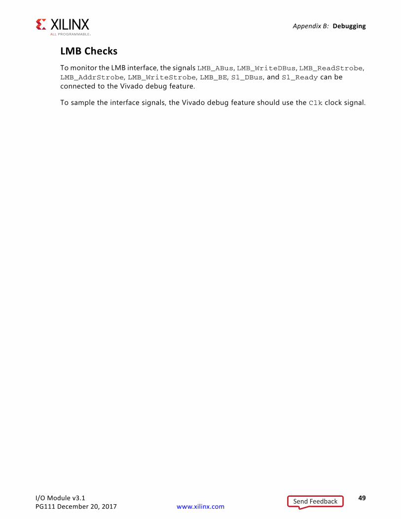
LMB ChecksTo monitor the LMB interface, the signals LMB_ABus, LMB_WriteDBus, LMB_ReadStrobe, LMB_AddrStrobe, LMB_WriteStrobe, LMB_BE, Sl_DBus, and Sl_Ready can be connected to the Vivado debug feature.
To sample the interface signals, the Vivado debug feature should use the Clk clock signal.
Send Feedback

I/O Module v3.1 50PG111 December 20, 2017 www.xilinx.com
Appendix C
Application Software Development
Device DriversThe I/O Module core is supported by the IO Module driver, included with the Xilinx Software Development Kit.
Send Feedback
I/O Module v3.1 51PG111 December 20, 2017 www.xilinx.com
Appendix D
Additional Resources and Legal Notices
Xilinx ResourcesFor support resources such as Answers, Documentation, Downloads, and Forums, see Xilinx Support.
ReferencesThese documents provide supplemental material useful with this user guide:
1. MicroBlaze Processor Reference Guide (UG984)
2. 7 Series FPGAs Configuration User Guide (UG470)
3. Triple Modular Redundancy (TMR) (PG268)
4. Vivado Design Suite User Guide: Designing IP Subsystems using IP Integrator (UG994)
5. Vivado Design Suite User Guide: Designing with IP (UG896)
6. Vivado Design Suite User Guide: Getting Started (UG910)
7. Vivado Design Suite User Guide: Logic Simulation (UG900)
8. ISE to Vivado Design Suite Migration Guide (UG911)
9. Vivado Design Suite User Guide: Programming and Debugging (UG908)
Send Feedback
I/O Module v3.1 52PG111 December 20, 2017 www.xilinx.com
Appendix D: Additional Resources and Legal Notices
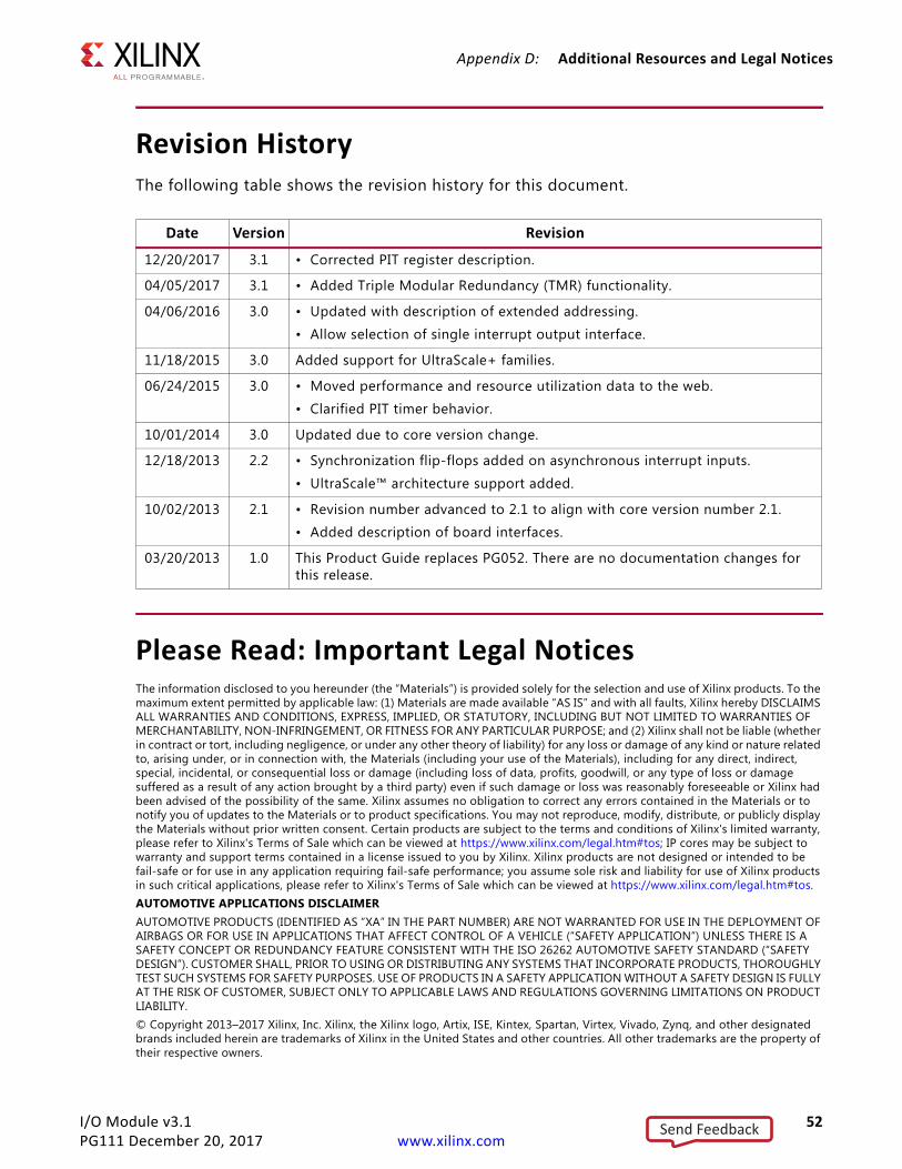
Revision HistoryThe following table shows the revision history for this document.
Please Read: Important Legal NoticesThe information disclosed to you hereunder (the “Materials”) is provided solely for the selection and use of Xilinx products. To the maximum extent permitted by applicable law: (1) Materials are made available “AS IS” and with all faults, Xilinx hereby DISCLAIMS ALL WARRANTIES AND CONDITIONS, EXPRESS, IMPLIED, OR STATUTORY, INCLUDING BUT NOT LIMITED TO WARRANTIES OF MERCHANTABILITY, NON-INFRINGEMENT, OR FITNESS FOR ANY PARTICULAR PURPOSE; and (2) Xilinx shall not be liable (whether in contract or tort, including negligence, or under any other theory of liability) for any loss or damage of any kind or nature related to, arising under, or in connection with, the Materials (including your use of the Materials), including for any direct, indirect, special, incidental, or consequential loss or damage (including loss of data, profits, goodwill, or any type of loss or damage suffered as a result of any action brought by a third party) even if such damage or loss was reasonably foreseeable or Xilinx had been advised of the possibility of the same. Xilinx assumes no obligation to correct any errors contained in the Materials or to notify you of updates to the Materials or to product specifications. You may not reproduce, modify, distribute, or publicly display the Materials without prior written consent. Certain products are subject to the terms and conditions of Xilinx's limited warranty, please refer to Xilinx's Terms of Sale which can be viewed at https://www.xilinx.com/legal.htm#tos; IP cores may be subject to warranty and support terms contained in a license issued to you by Xilinx. Xilinx products are not designed or intended to be fail-safe or for use in any application requiring fail-safe performance; you assume sole risk and liability for use of Xilinx products in such critical applications, please refer to Xilinx's Terms of Sale which can be viewed at https://www.xilinx.com/legal.htm#tos.AUTOMOTIVE APPLICATIONS DISCLAIMERAUTOMOTIVE PRODUCTS (IDENTIFIED AS “XA” IN THE PART NUMBER) ARE NOT WARRANTED FOR USE IN THE DEPLOYMENT OF AIRBAGS OR FOR USE IN APPLICATIONS THAT AFFECT CONTROL OF A VEHICLE (“SAFETY APPLICATION”) UNLESS THERE IS A SAFETY CONCEPT OR REDUNDANCY FEATURE CONSISTENT WITH THE ISO 26262 AUTOMOTIVE SAFETY STANDARD (“SAFETY DESIGN”). CUSTOMER SHALL, PRIOR TO USING OR DISTRIBUTING ANY SYSTEMS THAT INCORPORATE PRODUCTS, THOROUGHLY TEST SUCH SYSTEMS FOR SAFETY PURPOSES. USE OF PRODUCTS IN A SAFETY APPLICATION WITHOUT A SAFETY DESIGN IS FULLY AT THE RISK OF CUSTOMER, SUBJECT ONLY TO APPLICABLE LAWS AND REGULATIONS GOVERNING LIMITATIONS ON PRODUCT LIABILITY.© Copyright 2013–2017 Xilinx, Inc. Xilinx, the Xilinx logo, Artix, ISE, Kintex, Spartan, Virtex, Vivado, Zynq, and other designated brands included herein are trademarks of Xilinx in the United States and other countries. All other trademarks are the property of their respective owners.
Date Version Revision
12/20/2017 3.1 • Corrected PIT register description.
04/05/2017 3.1 • Added Triple Modular Redundancy (TMR) functionality.
04/06/2016 3.0 • Updated with description of extended addressing.
• Allow selection of single interrupt output interface.
11/18/2015 3.0 Added support for UltraScale+ families.
06/24/2015 3.0 • Moved performance and resource utilization data to the web.
• Clarified PIT timer behavior.
10/01/2014 3.0 Updated due to core version change.
12/18/2013 2.2 • Synchronization flip-flops added on asynchronous interrupt inputs.
• UltraScale™ architecture support added.
10/02/2013 2.1 • Revision number advanced to 2.1 to align with core version number 2.1.
• Added description of board interfaces.
03/20/2013 1.0 This Product Guide replaces PG052. There are no documentation changes for this release.
Send Feedback
Recommended