Embed Size (px)
Citation preview

DS756 July 25, 2012 www.xilinx.com 1Product Specification
© Copyright 2010–2012 Xilinx, Inc. Xilinx, the Xilinx logo, Artix, ISE, Kintex, Spartan, Virtex, Vivado, Zynq, and other designated brands included herein are trademarks of Xilinx in the United States and other countries. All other trademarks are the property of their respective owners.
IntroductionThe AXI IIC Bus Interface connects to the AdvancedMicrocontroller Bus Architecture (AMBA®)specification’s Advanced eXtensible Interface (AXI)and provides a low-speed, two-wire, serial businterface to a large number of popular devices. Thisproduct specification defines the architecture,hardware (signal) interface, software (register) interfaceand parameterization options for the LogiCORE™ IPAXI IIC Bus Interface module. AXI IIC supports allfeatures, except high-speed mode, of the Philips I2C-BusSpecification [Ref 1]. (See Specification Exceptions fordetails.)
Features• AXI interface based on the AXI4-Lite interface
• Master or slave operation
• Multi-master operation
• Software selectable acknowledge bit
• Arbitration lost interrupt with automatic mode switching from master to slave
• Calling address identification interrupt with automatic mode switching from master to slave
• START and STOP signal generation and detection
• Repeated START signal generation
• Acknowledge bit generation and detection
• Bus busy detection
• Fast-Mode Plus 1 MHz, Fast Mode 400 kHz, or Standard Mode 100 kHz operation
• 7-bit or 10-bit addressing
• General call enable or disable
• Transmit and receive FIFOs - 16 bytes deep
• Throttling
• General purpose output, 1 bit to 8 bits wide
• Dynamic Start and Stop generation
• Filtering on the SCL and SDA signals to eliminate spurious pulses
0
LogiCORE IP AXI IIC BusInterface (v1.02a)
DS756 July 25, 2012 0 0 Product Specification
LogiCORE IP Facts Table
Core Specifics
Supported Device Family(1)
Zynq™-7000(2), Artix™-7, Virtex®-7, Kintex™-7Virtex-6, Spartan®-6
Supported User Interfaces
AXI4-Lite
Resources
LUTs FFs DSP Slices Block RAMs
See Table 27 through Table 31 0
Provided with Core
Documentation Product Specification
Design Files VHDL
Example Design Not Provided
Test Bench Not Provided
Constraints File None
Simulation Model
None
Supported S/W Driver(3) Standalone and Linux
Tested Design Tools(4)
Design Entry Tools
Vivado™ Design Suite(5) v2012.2, XPS v14.2
Simulation Mentor Graphics ModelSim
Synthesis Tools XST v14.2Vivado Synthesis
Support
Provided by Xilinx @ www.xilinx.com/support
Notes: 1. For a complete list of supported derivative devices, see the IDS
Embedded Edition Derivative Device Support.2. Supported in ISE Design Suite implementations only.3. Standalone driver details can be found in the EDK or SDK
directory (<install_directory>/doc/usenglish/xilinx_drivers.htm). Linux OS and driver support information is available from //wiki.xilinx.com.
4. For the supported versions of the tools, see the Xilinx Design Tools: Release Notes Guide.
5. Vivado Design Suite supports only 7 series devices.

DS756 July 25, 2012 www.xilinx.com 2Product Specification
LogiCORE IP AXI IIC Bus Interface (v1.02a)
LimitationsThis core provides 0 ns SDA hold time in master mode operation as mentioned in Philips I2C-bus Specification [Ref 1].If any IIC slave requires additional hold time, this can be achieved by adding delay on SCL(C_SCL_INERTIAL_DELAY). See C_SCL_INERTIAL_DELAY and C_SDA_INERTIAL_DELAY for the descriptionof this parameter.
The dynamic controller logic in the AXI IIC controller supports master mode operation and 7-bit addressing only.
Specification Exceptions
Exceptions to the Philips I2C-bus Specification, version 2.1, January 2000• High-speed mode (Hs-mode) is not currently supported by the AXI IIC IP.
• 3-state buffers are used to perform the wired-AND function inherent in this bus structure.
• The Xilinx® FPGA device ratings must not be exceeded when interconnecting the AXI IIC to other devices.
• The tBUF parameter (“Bus free time between a STOP and START condition”, Table 5, Page 32 Philips I2C-bus Specification [Ref 1]) is not met by the controller. The user must ensure the proper delay specification is met if the core is utilized with a bus device that needs the extra delay.
Functional DescriptionThe AXI IIC Bus Interface module:
• Provides the transaction interface to the AXI4-Lite interface using the AXI Lite IPIF library [Ref 7].
• Does not provide explicit electrical connectivity to the IIC bus. Expects the design to include bidirectional I/O buffers that implement open collector drivers for the SDA and SCL signals. These bidirectional buffers are typically provided automatically by EDK XPS. The user must also provide external pull up devices to properly hold the bus at the logic '1' state when the driver is released.
The user must pay proper attention to the Philips specification when setting the values of these pull-up devices(typically resistors) to meet the Philips specification, the FPGA maximum ratings, and the ratings of any devices onthe bus itself.

DS756 July 25, 2012 www.xilinx.com 3Product Specification
LogiCORE IP AXI IIC Bus Interface (v1.02a)
Figure 1 illustrates the top-level block diagram for the AXI IIC bus interface. The modules are described in thesections that follow.
AXI Interface Module: Provides the interface to the AXI4-Lite and implements AXI protocol logic. The AXIinterface module is a bidirectional interface between a user IP core and the AXI4-Lite interface. To simplify theprocess of attaching AXI IIC bus interface to the AXI, the core makes use of a portable, pre-designed AXI interfacecalled AXI Lite IPIF library [Ref 7], that takes care of the AXI interface signals.
Register Interface Module: Implements the address map and connectivity for the firmware to control IIC datatransfer operations.
Soft Reset Module: Initializes the registers.
Interrupt Control Module: Generates interrupts.
IIC Control Module: Contains the state machine for the IIC bus operations.
Dynamic Master: Controls the operation in dynamic mode.
TX FIFO and RX FIFO: Hold the transmit and receive data, respectively.
Multi-Master Operation
The AXI IIC module only participates in multi-master arbitration when the bus is initially free and the attempt ismade. After the module issues the START, other masters can participate in addressing and the AXI IIC correctlyrelinquishes the bus if the requested address of the other master is lower than the address driven by AXI IIC.However, if the bus is not free, as indicated by SDA being Low and SCL being High (the START has occurred), whenthe request to acquire the bus is made, then the AXI IIC waits until the next bus free opportunity to arbitrate.
X-Ref Target - Figure 1
Figure 1: AXI IIC Bus Interface Top-Level Block Diagram
AXIInterfaceModule
IIC Control
Sda_TSda_OSda_I
Scl_TScl_OScl_I
Reg Interface
Interrupt Control
Interrupts
IIC2INTC_Irpt
GPOC_GPO_WIDTH
TXFIFO
Soft Reset
DynamicMaster
RXFIFO
AXI4-Lite Interface

DS756 July 25, 2012 www.xilinx.com 4Product Specification
LogiCORE IP AXI IIC Bus Interface (v1.02a)
Dynamic IIC Controller Logic
The dynamic controller logic provides an interface to the AXI IIC controller that is simple to use. The dynamic logicsupports master mode only and 7-bit addressing only.
The dynamic logic is controlled by a start bit and a stop bit located in the transmit FIFO. If neither of these bits areset, then the dynamic logic is disabled. Both of these bits are included in the FIFO and are acted upon as theTX_FIFO is emptied. See Dynamic Controller Logic Flow for details.
Signal Filtering
The Philips I2C-bus specification indicates that 0 to 50 ns of pulse rejection can be applied when operating in FastMode (>100 kHz). The user can specify the maximum amount allowed by the specification or more through thefiltering parameters C_SCL_INERTIAL_DELAY and C_SDA_INERTIAL_DELAY. These parameters specify theamount of delay in clock cycles.
Some designs might not require any filtering and others (even those operating below < 100 kHz) might require themaximum amount -- and possibly more. It depends on many factors beyond the control of the core itself. It mightbe necessary for the user to experiment to determine the optimum amount. If more than 50 ns of pulse rejection isrequired, you might need to more tightly constrain rise/fall times beyond what is required by the Philipsspecification to accommodate the additional delay occurring because of the filter operation.
Design ParametersTable 1 shows the design parameters of axi_iic.
Table 1: Design Parameters
Generic Feature / Description Parameter Name Allowable Values Default Value VHDL Type
System Parameter
G1Target FPGA family C_FAMILY zynq, virtex7,
kintex7, artix7, virtex6, spartan6
virtex6string
AXI Parameters
G2 AXI address bus width C_S_AXI_ADDR_WIDTH 9 9 integer
G3 AXI data bus width C_S_AXI_DATA_WIDTH 32 32 integer
G4 AXI interface type C_S_AXI_PROTOCOL axi4lite axi4lite string
AXI IIC Features
G5
Maximum frequency of the master mode generated SCL clock signal (Hz)
C_IIC_FREQLess than or equal to 400 kHz for Fast Mode definition(1)
100_000 integer
G6 10 Bit Addressing C_TEN_BIT_ADR
1 = The slave responds to 10-bit addresses0 = The slave responds to 7-bit addresses
0 integer
G7 Width of GPO C_GPO_WIDTH 1 to 8 1 integer
G8 AXI Clock Frequency (Hz) C_S_AXI_ACLK_FREQ_HZ
See Allowable Parameter Combinations
25_000_000 integer

DS756 July 25, 2012 www.xilinx.com 5Product Specification
LogiCORE IP AXI IIC Bus Interface (v1.02a)
Parameter Descriptions
C_IIC_FREQ
This parameter determines the approximate frequency of the master mode generated SCL clock signal (Hz). ForC_IIC_FREQ < 100,000, the appropriate timing specifications for Standard Mode operation are used. ForC_IIC_FREQ > 100,000 and C_IIC_FREQ < 400,000, the specifications for Fast Mode operation are used. ForC_IIC_FREQ > 400,000, the timing specifications for Fast-Mode Plus operation are used. See the Philips I2C-busSpecification [Ref 1] for details.
Note:1. The actual SCL clock frequency might vary from the value specified in the C_IIC_FREQ parameter for several reasons. In
particular, the low period and high period of the clock are determined by counting off system clocks from the moment the SCL signal is sampled Low or sampled High. As a result, the rise and fall times of the signals affect the SCL clock frequency.
2. The C_IIC_FREQ does not equate to the data bandwidth in bps. Overhead in transmitting START, STOP and addresses reduces the effective bandwidth below the line rate.
3. The IIC slaves can also control the clock rate to throttle data transfers to a manageable speed, thus changing the effective SCL clock rate.
4. The actual frequency only matches the specified value when C_S_AXI_ACLK_FREQ_HZ is an integer multiple of C_IIC_FREQ.
C_TEN_BIT_ADR
This parameter enables or disables the 10-bit addressing mode. Logic resource savings result when 10-bitaddressing is disabled.
C_GPO_WIDTH
This parameter sets the width of the general purpose output vector. If the user does not connect anything to thisport, then logic optimization removes any resources associated with it.
C_S_AXI_ACLK_FREQ_HZ
This parameter specifies (but does not set) the frequency of the AXI4-Lite interface. The AXI IIC utilizesS_AXI_ACLK for its system clock, and it must know the ratio of the C_IIC_FREQ to the C_S_AXI_ACLK_FREQ_HZ
to meet IIC timing specifications.
G9 SCL filtering C_SCL_INERTIAL_DELAY 0-255(2) 0 integer
G10 SDA filtering C_SDA_INERTIAL_DELAY 0-255(2) 0 integer
G11 SDA level C_SDA_LEVEL
1= SDA is driven High, when transmit throttling occurs and AXI IIC is acting as master transmitter0= SDA is driven Low, when transmit throttling occurs and AXI IIC is acting as master transmitter
1 integer
Notes: 1. The AXI IIC only meets this frequency exactly when C_IIC_FREQ divides evenly into C_S_AXI_ACLK_FREQ_HZ.2. A value of 0 indicates that no filtering is applied to the given signal. Setting of these parameters is based on the frequency of
S_AXI_ACLK. The range 0 to 255 is provided to accommodate higher frequencies. The pulse width rejection up to 500 ns on SCL and SDA is tested on Virtex-6 FPGA boards.
Table 1: Design Parameters (Cont’d)
Generic Feature / Description Parameter Name Allowable Values Default Value VHDL Type

DS756 July 25, 2012 www.xilinx.com 6Product Specification
LogiCORE IP AXI IIC Bus Interface (v1.02a)
C_SCL_INERTIAL_DELAY and C_SDA_INERTIAL_DELAY
In particular Virtex®-6 devices, the I/Os are so fast that the slow signal rise time plus noise exceeding the inputhysteresis can result in phantom pulses internal to the circuit. With the C_SCL_INERTIAL_DELAY/C_SDA_INERTIAL_DELAY parameter settings, the inertial delay filters remove these pulses effectively.
C_SCL_INERTIAL_DELAY/C_SDA_INERTIAL_DELAY parameters specify the number of S_AXI_ACLK cyclesused to define the width of the pulse rejection on SCL/SDA signals. For example, a 100 MHz S_AXI_ACLK clockwith a C_SCL_INERTIAL_DELAY value of 5 gives 50 ns of pulse rejection on SCL, which delays the SCL signalinternally by 50 ns. Similarly, a 100 MHz S_AXI_ACLK clock with an C_SDA_INERTIAL_DELAY value of 3 gives30 ns of pulse rejection on SDA.
The AXI IIC core provides 0 ns hold time on the SDA line in master mode operation. If any IIC slave requiresadditional hold time on the SDA from the core, delay can be added on SCL (C_SCL_INERTIAL_DELAY). Forexample, with a 100 MHz AXI clock to have a 300 ns hold time, the C_SCL_INERTIAL_DELAY parameter should beconfigured for an integer value of 30.
The design takes care of filtering the pulses on SCL and adding delay on SCL to have additional hold time withoutfiltering SDA; however, filtering the SDA line without filtering SCL can cause false start and stop conditions. Thepulse width to be rejected on SCL/SDA should consider the fall time and setup requirements of the AXI IIC core.
C_SDA_LEVEL
This parameter is used during transmit throttling when the AXI IIC acts as master transmitter. In this condition, theAXI IIC master transmitter drives the SDA line with C_SDA_LEVEL value.
C_S_AXI_ADDR_WIDTH
This integer parameter is used by the AXI IIC to size the AXI address related components within the slaveattachment. This value should be set to 32 bits.
C_S_AXI_DATA_WIDTH
This integer parameter is used by the AXI IIC to size AXI data bus related components within the slave attachment.This value should be set to 32 bits.
C_FAMILY
This parameter is defined as a string. It specifies the target FPGA technology for implementation of the AXI IIC.This parameter is required for proper selection of FPGA primitives. The configuration of these primitives can varyfrom one FPGA technology family to another.
Allowable Parameter Combinations
Because of the pipelined design of the AXI IIC, the AXI clock frequency must be at least 25 MHz and 25 times fasterthan the SCL clock frequency.
I/O SignalsThe AXI IIC I/O signals are described in Table 2.

DS756 July 25, 2012 www.xilinx.com 7Product Specification
LogiCORE IP AXI IIC Bus Interface (v1.02a)
Table 2: I/O Signal Descriptions
Port Signal Name Interface I/O Initial State Description
System Signals
P1 S_AXI_ACLK System I - AXI Clock.
P2 S_AXI_ARESETN System I - AXI Reset, active-Low.
P3 IIC2INTC_Irpt System O 0x0 System Interrupt output.
AXI Write Address Channel Signals
P4 S_AXI_AWADDR[C_S_AXI_ADDR_WIDTH-1:0] AXI I - AXI Write address. The write address bus gives
the address of the write transaction.
P5 S_AXI_AWVALID AXI I - Write address valid. This signal indicates that valid write address is available.
P6 S_AXI_AWREADY AXI O 0x0 Write address ready. This signal indicates that the slave is ready to accept an address.
AXI Write Channel Signals
P7 S_AXI_WDATA[C_S_AXI_DATA_WIDTH - 1: 0] AXI I - Write data.
P8 S_AXI_WSTB[C_S_AXI_DATA_WIDTH/8-1:0] AXI I - Write strobes. This signal indicates which byte
lanes to update in memory.(1)
P9 S_AXI_WVALID AXI I - Write valid. This signal indicates that valid write data and strobes are available.
P10 S_AXI_WREADY AXI O 0x0 Write ready. This signal indicates that the slave can accept the write data.
AXI Write Response Channel Signals
P11 S_AXI_BRESP[1:0] AXI O 0x0
Write response. This signal indicates the status of the write transaction.“00” - OKAY“10” - SLVERR“11” - DECERR
P12 S_AXI_BVALID AXI O 0x0 Write response valid. This signal indicates that a valid write response is available.
P13 S_AXI_BREADY AXI I - Response ready. This signal indicates that the master can accept the response information.
AXI Read Address Channel Signals
P14 S_AXI_ARADDR[C_S_AXI_ADDR_WIDTH -1:0] AXI I - Read address. The read address bus gives the
address of a read transaction.
P15 S_AXI_ARVALID AXI I -
Read address valid. This signal indicates, when HIGH, that the read address is valid and remains stable until the address acknowledgement signal, S_AXI_ARREADY, is High.
P16 S_AXI_ARREADY AXI O 0x1 Read address ready. This signal indicates that the slave is ready to accept an address.
AXI Read Data Channel Signals
P17 S_AXI_RDATA[C_S_AXI_DATA_WIDTH -1:0] AXI O 0x0 Read data.

DS756 July 25, 2012 www.xilinx.com 8Product Specification
LogiCORE IP AXI IIC Bus Interface (v1.02a)
Dependencies between Parameters and I/O SignalsThe width of some of the AXI IIC signals depends on parameters selected in the design. The dependencies betweenthe AXI IIC design parameters and I/O signals are shown in Table 3.
P18 S_AXI_RRESP[1:0] AXI O 0x0
Read response. This signal indicates the status of the read transfer.“00” - OKAY“10” - SLVERR“11” - DECERR
P19 S_AXI_RVALID AXI O 0x0Read valid. This signal indicates that the required read data is available and the read transfer can complete.
P20 S_AXI_RREADY AXI I -Read ready. This signal indicates that the master can accept the read data and response information.
IIC Signals
P21 Sda_I IIC I - IIC Serial Data Input from 3-state buffer.
P22 Sda_O IIC O 0x0 IIC Serial Data Output to 3-state buffer.
P23 Sda_T IIC O 0x0 IIC Serial Data Output Enable to 3-state buffer. (2)
P24 Scl_I IIC I - IIC Serial Clock Input from 3-state buffer.
P25 Scl_O IIC O 0x0 IIC Serial Clock Output to 3-state buffer.
P26 Scl_T IIC O 0x0 IIC Serial Clock Output Enable to 3-state buffer. (2)
P27 Gpo(32 - C_GPO_WIDTH: 31) IIC O 0x0 General Purpose Outputs.
Notes: 1. This signal is not used. The AXI IIC assumes that all byte lanes are active.2. The Sda_T and Scl_T signals are the 3-state enable signals that control the data direction for the Sda and Scl signals.
Table 3: Parameter-I/O Signal Dependencies
Generic or Port Name Affects Depends Relationship Description
Design Parameters
G2 C_S_AXI_ADDR_WIDTH P4, P14 - Defines the width of the ports.
G3 C_S_AXI_DATA_WIDTH P7, P8, P17 - Defines the width of the ports.
G7 C_GPO_WIDTH P27 - Specifies signal vector width.
I/O Signals
P4 S_AXI_AWADDR[C_S_AXI_ADDR_WIDTH-1:0] - G2 Port width depends on the generic C_S_AXI_ADDR_WIDTH.
P7 S_AXI_WDATA[C_S_AXI_DATA_WIDTH-1:0] - G3 Port width depends on the generic C_S_AXI_DATA_WIDTH.
P8 S_AXI_WSTB[C_S_AXI_DATA_WIDTH/8-1:0] - G3 Port width depends on the generic C_S_AXI_DATA_WIDTH.
Table 2: I/O Signal Descriptions (Cont’d)
Port Signal Name Interface I/O Initial State Description

DS756 July 25, 2012 www.xilinx.com 9Product Specification
LogiCORE IP AXI IIC Bus Interface (v1.02a)
IIC Protocol and Electrical CharacteristicsTo understand and utilize the register based software interface in the AXI IIC module it is helpful to have a basicunderstanding of the IIC protocol, and the electrical characteristics of the bus. For more details and timingdiagrams, see the Philips I2C-bus Specification [Ref 1].
Electrical Issues
An IIC bus consists of two wires named serial data (SDA) and serial clock (SCL), which carry information betweenthe devices connected to the bus. The 400 pF maximum signal load capacitance limits the maximum number ofdevices connectable to the same bus.
Both SDA and SCL transport data bidirectionally between connected devices using wired-AND electricalconnectivity. To implement the wired-AND, each device utilizes an open-collector/open-drain output that onlysinks current to ground to pull the signal to logic 0. Electrically that means it must not drive a logic 1 on to either bussignal but can only release or float the output. When no device asserts a logic 0 onto the bus, external pull-up devices(typically resistors) bring the signal state High. This method creates a source of confusion because no device canactually set the state of SCL or SDA to its High (logic 1) state.
The system designer must pay careful attention to the value of these pull-ups to guarantee that the implementation(consisting of the AXI IIC core, the Xilinx FPGA, and other devices on the bus) does not violate the IIC timingparameters. Selecting the value of pull-up resistors for a particular application is beyond the scope of the AXI IICand this document.
The user should consider utilizing the small additional amount of logic necessary for filtering of SCL and SDA byspecifying non-zero values for the parameters C_SCL_INERTIAL_DELAY and C_SDA_INERTIAL_DELAY.Reliability of the system can increase substantially.
When all devices on the bus release their drivers and both SDA and SCL are High for a specified period of time thebus is considered to be in the bus free state.
Protocol for Address and Data Transfer
Each device on the bus has a unique 7-bit or 10-bit address, operates both as a transmitter and receiver, andadditionally acts as a master or slave. A master device initiates data transfer on the bus and generates the clocksignal for that transfer. The slaves respond to the address clocked into them by the master and either accept(“write”) data from or provide (“read”) data to the master.
The IIC protocol defines an arbitration procedure that ensures that if more than one master simultaneously tries tocontrol the bus, only one is allowed to do so and the message is not corrupted. The arbitration and clocksynchronization procedures defined in the Philips I2C-bus Specification [Ref 1] are supported by the AXI IIC module.
P14 S_AXI_ARADDR[C_S_AXI_ADDR_WIDTH -1:0] - G2 Port width depends on the generic C_S_AXI_ADDR_WIDTH.
P17 S_AXI_RDATA[C_S_AXI_DATA_WIDTH -1:0] - G3 Port width depends on the generic C_S_AXI_DATA_WIDTH.
P27 GPO - G7 Width varies with the value of C_GPO_WIDTH.
Table 3: Parameter-I/O Signal Dependencies
Generic or Port Name Affects Depends Relationship Description

DS756 July 25, 2012 www.xilinx.com 10Product Specification
LogiCORE IP AXI IIC Bus Interface (v1.02a)
Data transfers on the IIC bus are initiated with a START condition and are terminated with a STOP condition. Afterreaching the bus free state, a master signals a START defined by a High-to-Low transition on SDA while SCL isHigh. Likewise, the master signals a STOP by a Low-to-High transition on the SDA line while SCL is High. Betweenthe START and STOP conditions of the bus, data on the SDA signal must be stable during the High period of theSCL signal and must meet any required setup and hold times during the Low period of the SCL signal.
Figure 2 illustrates how the definitions of: (a) the bus free state, and (b) the times when SDA and SCL can changerelative to each other, ensure that the START and STOP conditions are not confused as data.
Each transfer on the IIC bus consists of nine clock pulses on SCL to move eight bits of data and one acknowledge bit.master and slave transmitters send data with the most significant bit first (MSB).
After providing data for the eight clock periods, the master or slave transmitter releases the SDA line during theacknowledgement clock period to permit the receiver to transfer a 1-bit acknowledgment.
If a slave-receiver issues a not-acknowledge (by releasing the SDA signal during the acknowledgement clockperiod) this indicates that the slave-receiver was unable to accept the prior 8 bits transferred (consisting of addressor data bits). After a byte of data is transferred the slave (receiver | transmitter) has the unique capability to throttlethe transfer by keeping the SCL line in its Low state by actively pulling the SCL line Low for an arbitrary period oftime. This ability allows it time to determine internally what value it should place on the SDA line for theacknowledgement.
If the master-receiver signals a not-acknowledge, this indicates to the slave-transmitter that this byte was the lastbyte of the transfer.
Standard communication on the bus between a master and a slave is composed of four parts: START, slave address,data transfer, and STOP. The IIC protocol defines a transfer format for both 7-bit and 10-bit addressing.
A 7- bit address is initiated as follows: After the START condition, a slave address is sent. This address is seven bitslong followed by an eighth bit which is the read/write bit. A High indicates a request for data (read) and a Lowindicates a data transmission (write).
Only the slave with the calling address that matches the address transmitted by the master (that won arbitration)responds by sending back an acknowledge bit by pulling the SDA line Low on the ninth clock.
For 10-bit addressing, two bytes are transferred to set the 10-bit address. The transfer of the first byte contains thefollowing bit definition. The first five bits (bits 7:3) notify the slave that this is a 10-bit transfer followed by the nexttwo bits (bits 2:1), which set the slave address bits 9:8, and the LSB bit (bit 8) is the R/W bit. The second bytetransferred sets bits 7:0 of the slave address.
After successful slave addressing is achieved, the data transfer proceeds byte-by-byte in the direction as specifiedby the read/write bit.
The master can terminate the communication by generating a STOP signal to free the bus when the receiver signalsa not-acknowledge (signaled by releasing SDA during the acknowledgement clock period). However, the master
X-Ref Target - Figure 2
Figure 2: Data Transfer on the IIC Bus
1 2 3 7 8 9
SDA
SCL
STOPCONDITION
S P
STARTCONDITION
ACK
MSB

DS756 July 25, 2012 www.xilinx.com 11Product Specification
LogiCORE IP AXI IIC Bus Interface (v1.02a)
can generate a START signal without generating a STOP signal first. This is called a repeated START. A repeatedstart allows the master to change the direction of data transfer or address a different slave without giving up thebus.
Register DescriptionsTable 4 specifies the name, address, and accessibility of each firmware addressable register from the three classes ofregisters within the AXI IIC core.
Table 4: Registers
Address (hex) Register Name Access Type Default Value (hex)
Interrupt Registers
0x01C Global Interrupt Enable (GIE)(1) Read/Write 0x0
0x020 Interrupt Status Register (ISR)(1) Read/Toggle(3) on Write 0xD0
0x028 Interrupt Enable Register (IER)(1) Read/Write 0x0
Soft Reset
0x040 Soft Reset Register (SOFTR)(2) Write Only N/A
IIC Configuration, Control, Data
0x100 Control Register (CR) Read/Write 0x0
0x104 Status Register (SR) Read 0xC0
0x108 Transmit FIFO (TX_FIFO) Read/Write 0x0
0x10C Receive FIFO (RX_FIFO) Read N/A
0x110 Slave Address Register (ADR) Read/Write 0x0
0x114 Transmit FIFO Occupancy Register (TX_FIFO_OCY) Read 0x0
0x118 Receive FIFO Occupancy Register (RX_FIFO_OCY) Read 0x0
0x11C Slave Ten Bit Address Register (TEN_ADR) Read/Write 0x0
0x120 Receive FIFO Programmable Depth Interrupt Register (RX_FIFO_PIRQ) Read/Write 0x0
0x124 General Purpose Output Register (GPO) Read/Write 0x0
0x128 Timing Parameter TSUSTA Register Read/Write See Note(4)
0x12C Timing Parameter TSUSTO Register Read/Write See Note(4)
0x130 Timing Parameter THDSTA Register Read/Write See Note(4)
0x134 Timing Parameter TSUDAT Register Read/Write See Note(4)
0x138 Timing Parameter TBUF Register Read/Write See Note(4)
0x13C Timing Parameter THIGH Register Read/Write See Note(4)
0x140 Timing Parameter TLOW Register Read/Write See Note(4)

DS756 July 25, 2012 www.xilinx.com 12Product Specification
LogiCORE IP AXI IIC Bus Interface (v1.02a)
0x144 Timing Parameter THDDAT Register Read/Write See Note(4)
Notes: 1. See Xilinx Interrupt Control Data Sheet [Ref 3].2. The soft reset functionality is implemented by the proc_common soft_reset module.3. Toggle each bit position to which a ‘1’ is written.4. The default values of the timing parameter registers are based on the mode of operation (Standard, Fast, Fast-Mode Plus). The
value is derived based on the frequencies given for C_IIC_FREQ and C_S_AXI_CLK_FREQ_HZ. Fine-tuning can be done by writing to these registers.
Table 4: Registers (Cont’d)
Address (hex) Register Name Access Type Default Value (hex)

DS756 July 25, 2012 www.xilinx.com 13Product Specification
LogiCORE IP AXI IIC Bus Interface (v1.02a)
Global Interrupt Enable (GIE)
The Global Interrupt Enable Register, illustrated in Figure 3 and described in Table 5, has a single defined bit, in themost significant bit that is used to globally enable the final interrupt (coalesced from the ISR) out to the system.
Interrupt Status Register (ISR)
Firmware uses the ISR, illustrated in Figure 4, to determine which interrupt events from the AXI IIC need servicing.The register uses a toggle on write method to allow the firmware to easily clear selected interrupts by writing a ‘1’to the desired interrupt bit field position.This mechanism avoids the requirement on the User Interrupt Serviceroutine to perform a Read/Modify/Write operation to clear a single bit within the register. An interrupt value of ‘1’means the interrupt has occurred. A value of ‘0’ means that no interrupt occurred or it was cleared.
Table 6 illustrates the interrupt to bit field mappings of the IPIER (interrupt enable) and IPISR (interrupt status)registers. The number in the parenthesis is the interrupt bit number.
X-Ref Target - Figure 3
Figure 3: Global Interrupt Enable (GIE) Register
Table 5: Global Interrupt Enable (GIE) Register (0x01C)
Bit(s) Name Core Access Reset Value Description
31 GIE Read/Write 0
Global interrupt enable. 0 = All Interrupts disabled; no interrupt (even if unmasked in IER) possible from AXI IIC.1 = Unmasked AXI IIC interrupts are passed to processor.
30:0 Reserved N/A N/A Reserved
X-Ref Target - Figure 4
Figure 4: Interrupt Enable Register (IER) and Interrupt Status Register (ISR)
Table 6: Interrupt Status Register (0x020)
Bit(s) Name Core Access Reset Value Description
31:8 Reserved N/A N/A Reserved.
7 int(7) Read/Toggle on Write 1 Interrupt(7) -- Transmit FIFO Half Empty.
6 int(6) Read/Toggle on Write 1 Interrupt(6) -- Not Addressed As Slave.
5 int(5) Read/Toggle on Write 0 Interrupt(5) -- Addressed As Slave.
031 30
ReservedGIE
3 2 1 067 5 4
Not Addressedas Slave Int(6)
Bus NotBusy Int(4)
TX FIFOEmpty Int(2) Arb
LostInt(0)
RX FIFOFull Int(3)
TX FIFOHalf Empty
Int(7)
Addressedas Slave Int(5)
TX Error SlaveTX Comp Int(1)
Reserved
831

DS756 July 25, 2012 www.xilinx.com 14Product Specification
LogiCORE IP AXI IIC Bus Interface (v1.02a)
Interrupt Enable Register (IER)
The Interrupt Enable Register is described in Table 7. The firmware uses the fields of this register to enable ordisable interrupts needed to manage either the Standard Controller Logic Flow or the Dynamic Controller LogicFlow.
4 int(4) Read/Toggle on Write 1 Interrupt(4) -- IIC Bus is Not Busy.
3 int(3) Read/Toggle on Write 0 Interrupt(3) -- Receive FIFO Full.
2 int(2) Read/Toggle on Write 0 Interrupt(2) -- Transmit FIFO Empty.
1 int(1) Read/Toggle on Write 0 Interrupt(1) -- Transmit Error/Slave Transmit Complete.
0 int(0) Read/Toggle on Write 0 Interrupt(0) -- Arbitration Lost.
Table 7: Interrupt Enable Register (1) (0x028)
Bit(s) Name Core Access Reset Value Description
31:8 Reserved N/A N/A Reserved.
7 int(7) Read/Write 0 Interrupt(7) -- Transmit FIFO Half Empty.
6 int(6) Read/Write 0 Interrupt(6) -- Not Addressed As Slave.
5 int(5) Read/Write 0 Interrupt(5) -- Addressed As Slave.
4 int(4) Read/Write 0 Interrupt(4) -- IIC Bus is Not Busy.
3 int(3) Read/Write 0 Interrupt(3) -- Receive FIFO Full.
2 int(2) Read/Write 0 Interrupt(2) -- Transmit FIFO Empty.
1 int(1) Read/Write 0 Interrupt(1) -- Transmit Error/Slave Transmit Complete.
0 int(0) Read/Write 0 Interrupt(0) -- Arbitration Lost.
Notes: 1. In any given bit position, 1 = Interrupt enabled, 0 = Interrupt masked.
Table 6: Interrupt Status Register (0x020) (Cont’d)
Bit(s) Name Core Access Reset Value Description

DS756 July 25, 2012 www.xilinx.com 15Product Specification
LogiCORE IP AXI IIC Bus Interface (v1.02a)
Soft Reset Register (SOFTR)
The firmware can write to the SOFTR to initialize all of the AXI IIC registers to their default states. To accomplishthis, the firmware must write the reset key (RKEY) value of 0xA to the least significant nibble of the 32-bit word.After recognizing a write of 0xA the proc_common soft_reset module issues a pulse 4 clocks long to reset the AXIIIC. At the end of the pulse the SOFTR acknowledges the AXI transaction. That prevents anything further fromhappening while the reset occurs.
Writing any value to bits 3:0 other than 0xA results in an AXI transaction acknowledge with an error status.Theregister is not readable.
Applying soft reset to the AXI IIC core also clears the bus busy (BB) status (bit 2 of SR). When a read is issued to theSR immediately after reset, SR might not give the correct status of the IIC bus if the IIC bus is locked by another IICdevice. Therefore, the user should reset the external device after applying the soft reset to the AXI IIC core andbefore using the IIC bus again.
The SOFTR bit fields are shown in Figure 5 and described in Table 8.
X-Ref Target - Figure 5
Figure 5: Soft Reset Register (SOFTR)
Table 8: Soft Reset Register (0x040)
Bit(s) Name Core Access
Reset Value Description
31:4 Reserved N/A N/A Reserved.
3:0 RKEY Write N/A
Reset Key. The firmware must write a value of 0xA to this field to cause a soft reset of the Interrupt registers of AXI IIC controller. Writing any other value results in an AXI transaction acknowledgement with SLVERR and no reset occurs.
034
Reserved
RKEY
31

DS756 July 25, 2012 www.xilinx.com 16Product Specification
LogiCORE IP AXI IIC Bus Interface (v1.02a)
Control Register (CR)
Writing to the CR register configures the AXI IIC operation mode and simultaneously allows for IIC transactions tobe initiated.
Prior to setting master slave mode select (MSMS) to a 1, the TX_FIFO should contain the address of the AXI IICdevice. All the CR bits can be set at the same time as setting MSMS to a 1 to initiates a bus transaction.
When initiating a repeated start condition, the transmit FIFO must be empty. First, set the repeated start bit to a 1and then write the address of the AXI IIC device to the transmit FIFO. The rest of the FIFO can be filled with data,if required.
The EN field provides a way for the device driver to initialize interrupts prior to enabling the device tosend/receive data.
The AXI IIC Control Register is shown in Figure 6 and described in Table 9.
X-Ref Target - Figure 6
Figure 6: Control (CR) Register
Table 9: Control Register (0x100)
Bit(s) Name Core Access
Reset Value Description
31:7 Reserved N/A N/A Reserved.
6 GC_EN Read/Write 0
General Call Enable. Setting this bit High allows the AXI IIC to respond to a general call address.“0” - General Call Disabled.“1” - General Call Enabled.
5 RSTA Read/Write 0
Repeated Start. Writing a “1” to this bit generates a repeated START condition on the bus if the AXI IIC bus interface is the current bus master. Attempting a repeated START at the wrong time, if the bus is owned by another master, results in a loss of arbitration. This bit is reset when the repeated start occurs. This bit must be set prior to writing the new address to the TX_FIFO or DTR.
4 TXAK Read/Write 0
Transmit Acknowledge Enable. This bit specifies the value driven onto the SDA line during acknowledge cycles for both master and slave receivers.“1” - ACK bit = “1” - not-acknowledge.“0” - ACK bit = “0” - acknowledge.Because master receiver indicates the end of data reception by not acknowledging the last byte of the transfer, this bit is used to end a master receiver transfer. As a slave, this bit must be set prior to receiving the byte to signal a not-acknowledge.
3 TX Read/Write 0
Transmit/Receive Mode Select. This bit selects the direction of master/slave transfers.“1” selects an AXI IIC transmit.“0” selects an AXI IIC receive.This bit does not control the Read/Write bit that is sent on the bus with the address. The Read/Write bit that is sent with an address must be the LSB of the address written into the TX_FIFO.
3 2 1 06 5 4
GC_EN
Reserved
TXAK MSMS EN
TXRSTA TxFIFO
731

DS756 July 25, 2012 www.xilinx.com 17Product Specification
LogiCORE IP AXI IIC Bus Interface (v1.02a)
Status Register (SR)
This register contains the status of the AXI IIC bus interface. All bits are cleared upon reset.
The read-only SR register is shown in Figure 7 and described in Table 10.
2 MSMS Read/Write 0
Master/Slave Mode Select. When this bit is changed from 0 to 1, the AXI IIC bus interface generates a START condition in master mode. When this bit is cleared, a STOP condition is generated and the AXI IIC bus interface switches to slave mode. When this bit is cleared by the hardware, because arbitration for the bus has been lost, a STOP condition is not generated. (See also Interrupt(0): Arbitration Lost, page 26.)
1 TX_FIFO Reset Read/Write 0
Transmit FIFO Reset. This bit must be set to flush the FIFO if either (a) arbitration is lost or (b) if a transmit error occurs. “1” resets the transmit FIFO. “0” transmit FIFO normal operation.
0 EN Read/Write 0AXI IIC Enable. This bit must be set before any other CR bits have any effect. “1” enables the AXI IIC controller. “0” resets and disables the AXI IIC controller but not the registers or FIFOs.
X-Ref Target - Figure 7
Figure 7: Status Register (SR)
Table 10: Status Register (0x104)
Bit(s) Name Core Access
Reset Value Description
31:8 Reserved N/A N/A Reserved.
7 TX_FIFO_Empty Read 1 Transmit FIFO empty. This bit is set High when the transmit FIFO is empty.
6 RX_FIFO_Empty Read 1 Receive FIFO empty. This is set High when the receive FIFO is empty.
5 RX_FIFO_Full Read 0Receive FIFO full. This bit is set High when the receive FIFO is full. This bit is set only when all 16 locations in the FIFO are full, regardless of the compare value field of the RX_FIFO_PIRQ register.
4 TX_FIFO_Full Read 0 Transmit FIFO full. This bit is set High when the transmit FIFO is full.
3 SRW Read 0
Slave Read/Write. When the IIC bus interface has been addressed as a slave (AAS is set), this bit indicates the value of the read/write bit sent by the master. This bit is only valid when a complete transfer has occurred and no other transfers have been initiated.“1” indicates master reading from slave.“0” indicates master writing to slave.
Table 9: Control Register (0x100) (Cont’d)
Bit(s) Name Core Access
Reset Value Description
3 2 1 067 5 4
RX_FIFO_Empty
Reserved
TX_FIFO_Full BB ABGC
SRWTX_FIFO_Empty
RX_FIFO_Full
AAS
31 8
DS756 July 25, 2012 www.xilinx.com 18Product Specification
LogiCORE IP AXI IIC Bus Interface (v1.02a)
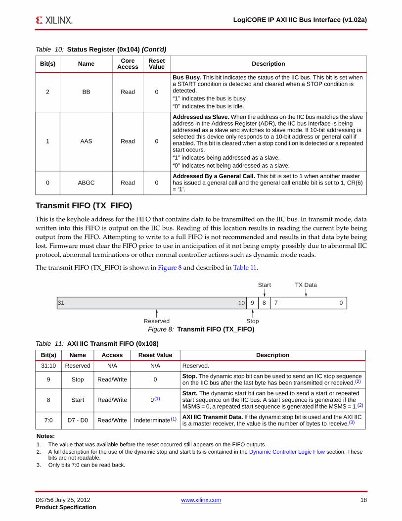
Transmit FIFO (TX_FIFO)
This is the keyhole address for the FIFO that contains data to be transmitted on the IIC bus. In transmit mode, datawritten into this FIFO is output on the IIC bus. Reading of this location results in reading the current byte beingoutput from the FIFO. Attempting to write to a full FIFO is not recommended and results in that data byte beinglost. Firmware must clear the FIFO prior to use in anticipation of it not being empty possibly due to abnormal IICprotocol, abnormal terminations or other normal controller actions such as dynamic mode reads.
The transmit FIFO (TX_FIFO) is shown in Figure 8 and described in Table 11.
2 BB Read 0
Bus Busy. This bit indicates the status of the IIC bus. This bit is set when a START condition is detected and cleared when a STOP condition is detected.“1” indicates the bus is busy.“0” indicates the bus is idle.
1 AAS Read 0
Addressed as Slave. When the address on the IIC bus matches the slave address in the Address Register (ADR), the IIC bus interface is being addressed as a slave and switches to slave mode. If 10-bit addressing is selected this device only responds to a 10-bit address or general call if enabled. This bit is cleared when a stop condition is detected or a repeated start occurs.“1” indicates being addressed as a slave.“0” indicates not being addressed as a slave.
0 ABGC Read 0Addressed By a General Call. This bit is set to 1 when another master has issued a general call and the general call enable bit is set to 1, CR(6) = ‘1’.
X-Ref Target - Figure 8
Figure 8: Transmit FIFO (TX_FIFO)
Table 11: AXI IIC Transmit FIFO (0x108)
Bit(s) Name Access Reset Value Description
31:10 Reserved N/A N/A Reserved.
9 Stop Read/Write 0 Stop. The dynamic stop bit can be used to send an IIC stop sequence on the IIC bus after the last byte has been transmitted or received.(2)
8 Start Read/Write 0(1)Start. The dynamic start bit can be used to send a start or repeated start sequence on the IIC bus. A start sequence is generated if the MSMS = 0, a repeated start sequence is generated if the MSMS = 1.(2)
7:0 D7 - D0 Read/Write Indeterminate(1) AXI IIC Transmit Data. If the dynamic stop bit is used and the AXI IIC is a master receiver, the value is the number of bytes to receive.(3)
Notes: 1. The value that was available before the reset occurred still appears on the FIFO outputs.2. A full description for the use of the dynamic stop and start bits is contained in the Dynamic Controller Logic Flow section. These
bits are not readable.3. Only bits 7:0 can be read back.
Table 10: Status Register (0x104) (Cont’d)
Bit(s) Name Core Access
Reset Value Description
0789
Reserved Stop
TX DataStart
1031

DS756 July 25, 2012 www.xilinx.com 19Product Specification
LogiCORE IP AXI IIC Bus Interface (v1.02a)
Receive FIFO (RX_FIFO)
This FIFO contains the data received from the IIC bus. The received IIC data is placed in this FIFO after eachcomplete transfer. The receive FIFO occupancy register (RX_FIFO_OCY) must be equal to the Receive FIFOProgrammable Depth Interrupt Register (RX_FIFO_PIRQ) before throttling occurs. The receive FIFO is read only.Reading this FIFO when it is empty results in indeterminate data being read.
The receive FIFO is shown in Figure 9 and described in Table 12.
Slave Address Register (ADR)
The user programs the ADR register (and possibly the TEN_ADR register) to set the address at which the slaveacknowledges an address transfer operation from the bus master. The slave address field of the ADR registercontains all seven bits of the 7-bit address or the least significant seven bits of the 10-bit address the AXI IIC businterface recognizes when operating as a slave.
The field layout of the register is shown in Figure 10 and described in Table 13.
X-Ref Target - Figure 9
Figure 9: Receive FIFO (RX_FIFO)
Table 12: Receive FIFO (0x10C)
Bit(s) Name Access Reset Value Description
31:8 Reserved N/A N/A Reserved.
7:0 D7 - D0 Read Indeterminate(1) IIC Receive Data.
Notes: 1. The value that was available before the reset occurred appears on the FIFO outputs.
X-Ref Target - Figure 10
Figure 10: Slave Address Register (ADR)
Table 13: Slave Address Register (0x110)
Bit(s) Name Access Reset Value Description
31:8 Reserved N/A N/A Reserved.
7:1 Slave Address Read/Write 0 Address used by the IIC bus interface when in slave mode.
0 Reserved N/A N/A Reserved.
07
Reserved
RX Data
831
3117
Reserved
Slave Address Reserved
0831

DS756 July 25, 2012 www.xilinx.com 20Product Specification
LogiCORE IP AXI IIC Bus Interface (v1.02a)
Slave 10-Bit Address Register (TEN_ADR)
The user programs the ADR register (and possibly the TEN_ADR register) to set the address at which the slave willacknowledge and address transfer operation from the bus master. The slave address field of the TEN_ADR registercontains the most significant three bits of the 10-bit address that the AXI IIC bus interface recognizes whenoperating as a 10-bit addressable slave. This register exists only if the user configures the AXI IIC for 10-bitaddressing by setting generic parameter C_TEN_BIT_ADR to 1.
The TEN_ADR register is shown in Figure 11 and described in Table 14.
Transmit FIFO Occupancy Register (TX_FIFO_OCY)
This field contains the occupancy value for the transmit FIFO. Reading this register cannot be used to determine ifthe FIFO is empty. The transmit FIFO Empty interrupt conveys that information. The value read is the occupancyvalue minus one, therefore reading all zeros indicates that the first location is filled and reading all ones implies thatall 16 locations are filled.
The TX_FIFO_OCY register is shown in Figure 12 and described in Table 15.
X-Ref Target - Figure 11
Figure 11: 10-Bit Address Register (TEN_ADR)
Table 14: Slave 10-Bit Address Register (0x11C)
Bit(s) Name Access Reset Value Description
31:3 Reserved N/A N/A Reserved.
2:0 MSB of Slave Address Read/Write 0 3 MSBs of the 10-bit address used by the AXI IIC bus interface when in slave mode.
X-Ref Target - Figure 12
Figure 12: Transmit FIFO Occupancy Register (TX_FIFO_OCY)
Table 15: Transmit FIFO Occupancy Register (0x114)
Bit(s) Name Access Reset Value Description
31:4 Reserved N/A N/A Reserved.
3:0 Occupancy Value Read 0 Bit 3 is the MSB. A binary value of 1001 indicates that 10 locations are full in the FIFO.
02
Reserved
Slave Address
331
03
Reserved
TransmitOccupancy
431

DS756 July 25, 2012 www.xilinx.com 21Product Specification
LogiCORE IP AXI IIC Bus Interface (v1.02a)
Receive FIFO Occupancy Register (RX_FIFO_OCY)
This field contains the occupancy value for the receive FIFO. This register is read only. Reading this register cannotbe used to determine if the FIFO is empty. RX_FIFO_Empty, bit 1 in the status register, is used to convey thatinformation. The value read is the occupancy value minus one, therefore reading all 0s implies that the first locationis filled and reading all 1s implies that all 16 locations are filled.
The RX_FIFO_OCY register is shown in Figure 13 and described in Table 16.
Receive FIFO Programmable Depth Interrupt Register (RX_FIFO_PIRQ)
This field contains the value which causes the receive FIFO Interrupt to be set. When this value is equal to theRX_FIFO_OCY value, the receive FIFO interrupt is set and remains set until the equality is no longer true. A readfrom the receive FIFO causes the IIC receive FIFO interrupt to be cleared. When the RX_FIFO_PIRQ is equal to theRX_FIFO_OCY, throttling also occurs to prevent the transmitter from transmitting.
The read/write RX_FIFO_PIRQ register is shown in Figure 14 and described in Table 17.
X-Ref Target - Figure 13
Figure 13: Receive FIFO Occupancy Register (RX_FIFO_OCY)
Table 16: Receive FIFO Occupancy Register (0x118)
Bit(s) Name Access Reset Value Description
31:4 Reserved N/A N/A Reserved.
3:0 Occupancy Value Read 0 Bit 3 is the MSB. A binary value of 1001 implies that 10 locations are full in the FIFO.
X-Ref Target - Figure 14
Figure 14: Receive FIFO Programmable Depth Interrupt Register (RX_FIFO_PIRQ)
Table 17: Receive FIFO Programmable Depth Interrupt Register (0x120)
Bit(s) Name Access Reset Value Description
31:4 Reserved N/A N/A Reserved.
3:0 Compare Value Read/Write 0Bit 3 is the MSB. A binary value of 1001 implies that when 10 locations in the receive FIFO are filled, the receive FIFO interrupt is set.
431 03
Reserved
ReceiveOccupancy
03
Reserved
CompareValue
431

DS756 July 25, 2012 www.xilinx.com 22Product Specification
LogiCORE IP AXI IIC Bus Interface (v1.02a)
General Purpose Output Register (GPO)
The current value of the general-purpose output field of the GPO register is reflected continuously on the GPO I/Osignal of the core. For example, the GPO signal of the core could be used to set an IIC memory device’s write protect.
If C_GPO_WIDTH is equal to one, the only bit populated in the register is GPO(0), the LSB. If C_GPO_WIDTH isequal to 8, then bits 7 through 0 in the GPO are populated. Reading unpopulated bits results in indeterminate data.
The GPO register is shown in Figure 15 and described in Table 18.
Timing Parameter TSUSTA Register (TSUSTA)
This value determines the setup time (in terms of number of core clock cycles) for a repeated START condition asper the I2C specification. It contains the default value based on the operating frequency of the core and theconfigured IIC frequency (C_S_AXI_CLK_FREQ_HZ and C_IIC_FREQ). Users can read this register value andupdate it, if the value does not work in their design environment.
The TSUSTA register is shown in Figure 16 and described in Table 19.
X-Ref Target - Figure 15
Figure 15: General Purpose Output Register (GPO)
Table 18: General Purpose Output Register (0x124)
Bit(s) Name Access Reset Value Description
31:C_GPO_WIDTH Reserved N/A N/A Reserved.
(C_GPO_WIDTH-1):0 General Purpose Outputs Read/Write 0 GPO. The LSB (bit 0) is the first bit populated.
X-Ref Target - Figure 16
Figure 16: TSUSTA Register
Table 19: TSUSTA Register (0x128)
Bit(s) Name Core AccessReset Value
Description
31:0 TSUSTA Read/Write See Note(1) Setup time for a repeated START condition.
Notes: 1. Depends on the mode of operation: Standard, Fast, or Fast-Mode Plus.
0
Reserved
General Purpose Output
31
A = C_GPO_WIDTH-1
A

DS756 July 25, 2012 www.xilinx.com 23Product Specification
LogiCORE IP AXI IIC Bus Interface (v1.02a)
Timing Parameter TSUSTO Register (TSUSTO)
This value determines the setup time (in terms of number of core clock cycles) for a repeated STOP condition as perthe I2C specification. It contains the default value based on the operating frequency of the core and the configuredIIC frequency (C_S_AXI_CLK_FREQ_HZ and C_IIC_FREQ). Users can read this register value and update it, if thevalue does not work in their design environment.
The TSUSTO register is shown in Figure 17 and described in Table 20.
Timing Parameter THDSTA Register (THDSTA)
This value determines the hold time (in terms of number of core clock cycles) for a repeated START condition as perthe I2C specification. It contains the default value based on the operating frequency of the core and the configuredIIC frequency (C_S_AXI_CLK_FREQ_HZ and C_IIC_FREQ). Users can read this register value and update it, if thevalue does not work in their design environment.
The THDSTA register is shown in Figure 18 and described in Table 21.
X-Ref Target - Figure 17
Figure 17: TSUSTO Register
Table 20: TSUSTO Register (0x12C)
Bit(s) Name Core AccessReset Value
Description
31:0 TSUSTO Read/Write See Note(1) Setup time for a repeated STOP condition.
Notes: 1. Depends on the mode of operation: Standard, Fast, or Fast-Mode Plus.
X-Ref Target - Figure 18
Figure 18: THDSTA Register
Table 21: THDSTA Register (0x130)
Bit(s) Name Core Access Reset Value Description
31:0 THDSTA Read/Write See Note(1) Hold time for a repeated START condition.
Notes: 1. Depends on the mode of operation: Standard, Fast, or Fast-Mode Plus.

DS756 July 25, 2012 www.xilinx.com 24Product Specification
LogiCORE IP AXI IIC Bus Interface (v1.02a)
Timing Parameter TSUDAT Register (TSUDAT)
This value determines the data setup time (in terms of number of core clock cycles) as per the I2C specification. Itcontains the default value based on the operating frequency of the core and the configured IIC frequency(C_S_AXI_CLK_FREQ_HZ and C_IIC_FREQ). Users can read this register value and update it, if the value does notwork in their design environment.
The TSUDAT register is shown in Figure 19 and described in Table 22.
Timing Parameter TBUF Register (TBUF)
This value determines the bus free time between a STOP and START condition (in terms of number of core clockcycles) as per the I2C specification. It contains the default value based on the operating frequency of the core and theconfigured IIC frequency (C_S_AXI_CLK_FREQ_HZ and C_IIC_FREQ). Users can read this register value andupdate it, if the value does not work in their design environment.
The TBUF register is shown in Figure 20 and described in Table 23.
X-Ref Target - Figure 19
Figure 19: TSUDAT Register
Table 22: TSUDAT Register (0x134)
Bit(s) Name Core Access Reset Value Description
31:0 TSUDAT Read/Write See Note(1) Data setup time.
Notes: 1. Depends on the mode of operation: Standard, Fast, or Fast-Mode Plus.
X-Ref Target - Figure 20
Figure 20: TBUF Register
Table 23: TBUF Register (0x138)
Bit(s) Name Core Access Reset Value Description
31:0 TBUF Read/Write See Note(1) Bus free time between a STOP and START condition.
Notes: 1. Depends on the mode of operation: Standard, Fast, or Fast-Mode Plus.

DS756 July 25, 2012 www.xilinx.com 25Product Specification
LogiCORE IP AXI IIC Bus Interface (v1.02a)
Timing Parameter THIGH Register (THIGH)
This value determines the High period of the SCL clock (in terms of number of core clock cycles) as per the I2Cspecification. It contains the default value based on the operating frequency of the core and the configured IICfrequency (C_S_AXI_CLK_FREQ_HZ and C_IIC_FREQ). Users can read this register value and update it, if thevalue does not work in their design environment.
The THIGH register is shown in Figure 21 and described in Table 24.
Timing Parameter TLOW Register (TLOW)
This value determines the Low period of the SCL clock (in terms of number of core clock cycles) as per the I2Cspecification. It contains the default value based on the operating frequency of the core and the configured IICfrequency (C_S_AXI_CLK_FREQ_HZ and C_IIC_FREQ). Users can read this register value and update it, if thevalue does not work in their design environment.
The TLOW register is shown in Figure 22 and described in Table 25.
X-Ref Target - Figure 21
Figure 21: THIGH Register
Table 24: THIGH Register (0x13C)
Bit(s) Name Core Access Reset Value Description
31:0 THIGH Read/Write See Note(1) High period of the SCL clock.
Notes: 1. Depends on the mode of operation: Standard, Fast, or Fast-Mode Plus.
X-Ref Target - Figure 22
Figure 22: TLOW Register
Table 25: TLOW Register (0x140)
Bit(s) Name Core AccessReset Value
Description
31:0 THIGH Read/Write See Note(1) Low period of the SCL clock.
Notes: 1. Depends on the mode of operation: Standard, Fast, or Fast-Mode Plus.

DS756 July 25, 2012 www.xilinx.com 26Product Specification
LogiCORE IP AXI IIC Bus Interface (v1.02a)
Timing Parameter THDDAT Register (THDDAT)
This value determines the data hold time (in terms of number of core clock cycles) as per the I2C specification. Itcontains the default value based on the operating frequency of the core and the configured IIC frequency(C_S_AXI_CLK_FREQ_HZ and C_IIC_FREQ). Users can read this register value and update it, if the value does notwork in their design environment.
The THDDAT register is shown in Figure 23 and described in Table 26.
Interrupt DescriptionsThe AXI IIC driver firmware has eight unique interrupt conditions available to manage IIC data transfers. Theseinterrupt events generated by the AXI IIC module’s internal IIC control module are managed by the InterruptControl (v2.01a) block.
This block then generates a single IIC2INTC_Irpt signal. The registers within this block provide an interfacecontaining many of the features commonly needed for interrupt handling.
Interrupt(0): Arbitration Lost
Interrupt(0) is the Arbitration Lost interrupt. This interrupt is set when arbitration for the IIC bus is lost. Thefirmware must respond by first clearing the Control Register (CR) MSMS bit and then clearing this interrupt bywriting a 1 to the Interrupt Status Register (ISR) INT(0) bit to toggle it. See also the TX_FIFO reset bit in the ControlRegister (CR).
Interrupt(1): Transmit Error/Slave Transmit Complete
Four possible events can cause this interrupt:
1. AXI IIC operating as a master transmitter: Interrupt(1) implies an error. There are two possibilities:
a. Either no slave was present at the transmitted address in which case the master transmitter recognizes a NOT ACKNOWLEDGE.
b. The slave receiver issued a NOT ACKNOWLEDGE to signal that it is not accepting any more data.
In either case the MSMS bit in the Control Register transitions from 1 to 0 causing the AXI IIC to initiate a stop condition, which implies that the bus is not busy.
X-Ref Target - Figure 23
Figure 23: THDDAT Register
Table 26: THDDAT Register (0x144)
Bit(s) Name Core AccessReset Value
Description
31:0 THDDAT Read/Write See Note(1) Data hold time.
Notes: 1. Depends on the mode of operation: Standard, Fast, or Fast-Mode Plus.

DS756 July 25, 2012 www.xilinx.com 27Product Specification
LogiCORE IP AXI IIC Bus Interface (v1.02a)
2. AXI IIC operating as a master receiver: Interrupt(1) implies a transmit complete. This interrupt is caused by setting the TXAK bit in the Control Register (CR) to 1 to indicate to the slave transmitter that the last byte has been transmitted.
3. AXI IIC operating as a slave transmitter: Interrupt(1) implies a transmit complete. This interrupt is caused by the master device to indicate to the IIC that the last byte has been transmitted.
4. AXI IIC operating as a slave receiver: Interrupt(1) implies an error. This interrupt is caused by the IIC (setting CR register field TXAK to 1).
The firmware must clear this interrupt by writing a 1 to the Interrupt Status Register (ISR), INT(1) bit to toggle it.
This interrupt occurs before INT(4), if INT(4) is also enabled. (The stop occurs later.)
Interrupt(2): Transmit FIFO Empty
The controller raises (sets) the interrupt flag and keeps it raised while a transmit throttle condition exists. After theflag has been raised and the transmit throttle condition is removed then (and only then can) the firmware lower(clear) the flag by writing a ‘1’ to the Interrupt Status Register (ISR), INT(2) bit to toggle the flag state. See ThrottleDescription for information on actions that must be taken to clear a transmit throttle condition. The usual cause fora transmit throttle condition is the transmit FIFO going empty.
Interrupt(3): Receive FIFO Full
This interrupt is set when the Receive FIFO Programmable Depth Interrupt Register (RX_FIFO_PIRQ) is equal tothe Receive FIFO Occupancy Register (RX_FIFO_OCY). Clearing this interrupt requires that the data receive FIFObe read.
Interrupt(4): IIC Bus is Not Busy
Interrupt(4) is set when the IIC bus is not busy. The condition remains set as long as the bus is not busy and cannotbe cleared while the condition is true. Firmware must verify that the SR(BB) is asserted, indicating bus busy, beforeattempting to reset this interrupt bit.
A master that loses arbitration that wants to get back on this bus should immediately clear this bit.
If necessary, the slave should clear this bit after getting the AAS interrupt to know when the bus is not busy occurs.(A master could talk to several slaves before relinquishing the bus.)
Interrupt(5): Addressed As Slave
This interrupt is set when the AXI IIC is addressed as a slave.
Interrupt(6): Not Addressed As Slave
This interrupt allows the detection of the end of receive data for a slave receiver when there has been no stopcondition (repeated start). The interrupt occurs when a start condition followed by a non-matching slave address isdetected. This interrupt is set when the AXI IIC is not addressed as a slave.
Interrupt(7): Transmit FIFO Half Empty
This interrupt is set while the MSB of the TX_FIFO_OCY = 0.

DS756 July 25, 2012 www.xilinx.com 28Product Specification
LogiCORE IP AXI IIC Bus Interface (v1.02a)
Throttle Description
The Philips I2C-bus Specification [Ref 1] permits devices to throttle (suspend) data transmission on the bus by holdingthe SCL line Low for an indefinite period of time. The AXI IIC controller uses this throttling mechanism to preventeither a receive overrun (RX_FIFO full) or a transmit underflow (TX_FIFO empty) by holding the SCL line Low afterthe acknowledge bit has been sent.
Throttling is independent of master or slave operation and depends upon transmit or receive operation only.However initiation of stops and repeated starts can only be accomplished at times when throttling is occurring andonly the AXI IIC acting as a master can initiate such actions. When the AXI IIC is addressed as a slave, the throttlingmechanism gives the firmware time to either gather data for transmission from the TX_FIFO, or find a place to storedata received into the RX_FIFO.
Transmit throttling occurs when the transmit FIFO goes empty (except when a stop condition is pending). Whenone or more bytes are written into the TX_FIFO, the transmit throttle condition is removed. The automatic throttlingprovides the firmware with time to handle the interrupt processing necessary for data transfer without manuallyhaving to manage the low level SCL signalling details. To prevent the throttle condition from re-appearing when theTX_FIFO goes empty the firmware must setup the master to issue a stop condition by resetting the CR (MSMS) bitwhile the bus is throttled and prior to writing the very last byte to be transmitted to the TX_FIFO.
To switch transmission to a new device while throttled a repeated start can be issued. The firmware does this bysetting the RSTA bit in the Control Register (CR), then writing the device address into the TX_FIFO. The controllerrecognizes this sequence, issues the repeated start, retrieves the address byte from the TX_FIFO and outputs it ontothe bus. If no more data was placed into the TX_FIFO the controller immediately throttles again.
Receive throttling is done when the Receive FIFO Occupancy Register (RX_FIFO_OCY) matches the value set in theReceive FIFO Programmable Depth Interrupt Register (RX_FIFO_PIRQ). The throttle condition is momentarilyremoved when a byte from the receive FIFO is read, thus allowing the transmitter to send the next byte. The slowrate of IIC transmissions should permit the firmware to completely empty the receive FIFO prior to the receipt ofthe next byte but it is not necessary to do so.
When the AXI IIC is a master and a receive throttle condition exists, the AXI IIC generates a stop condition if theControl Register (CR) MSMS bit is changed from a 1 to a 0. This allows single byte reads from a slave device. TheControl Register (CR) TXAK must be set equal to 1 to not-acknowledge the byte if desired.
When the AXI IIC is a master, is in a receive throttle condition and the transmit FIFO is empty, setting the repeatedstart in the control register causes a transmit throttle condition to occur. That would raise the Interrupt(2): TransmitFIFO Empty flag.
Standard Controller Logic FlowThis section briefly discusses setting the AXI IIC registers to initiate and complete bus transactions.
IIC Master Transmitter with a Repeated Start1. Write the IIC device address to the TX_FIFO.
2. Write data to TX_FIFO.
3. Write to Control Register (CR) to set MSMS = 1 and TX = 1.
4. Continue writing data to TX_FIFO.
5. Wait for transmit FIFO empty interrupt. This implies the IIC has throttled the bus.
6. Write to CR to set RSTA = 1.

DS756 July 25, 2012 www.xilinx.com 29Product Specification
LogiCORE IP AXI IIC Bus Interface (v1.02a)
7. Write IIC device address to TX_FIFO.
8. Write all data except last byte to TX_FIFO.
9. Wait for transmit FIFO empty interrupt. This implies the IIC has throttled the bus.
10. Write to CR to set MSMS = 0. The IIC generates a stop condition at the end of the last byte.
11. Write last byte of data to TX_FIFO.
IIC Master Receiver with a Repeated Start1. Write the IIC peripheral device addresses for the first slave device to the TX_FIFO. Write the Receive FIFO
Programmable Depth Interrupt Register (RX_FIFO_PIRQ) to the total message length (call it M) minus two. It is assume that the message is less than the maximum FIFO depth of 16 bytes.
2. Set Control Register (CR) MSMS = 1 and Control Register (CR) TX = 0.
3. Wait for the receive FIFO interrupt indicating M-1 bytes have been received.
4. Set Control Register (CR) TXAK = 1.
TXAK causes the AXI IIC controller to not-acknowledge the next byte received indicating to the slave transmitter that the master receiver accepts no further data. TXAK is set before reading data from the RX_FIFO, because as soon as a read from the RX_FIFO has occurred, the throttle condition is removed and the opportunity to set the bit is lost.
5. Read all M-1 data bytes from the RX_FIFO. Set the RX_FIFO_PIRQ to 0 so that the last byte, soon to be received, causes the receive FIFO full interrupt to be raised.
6. Clear the receive FIFO full interrupt now because after a single byte is retrieved from the RX_FIFO the throttle condition is removed by the controller and the interrupt flag can be lowered (cleared).
7. Wait for the receive FIFO full interrupt.
8. The controller is throttled again with a full RX_FIFO. Set Control Register (CR) RSTA = 1. Write the peripheral IIC device address for a new (or same) IIC slave to the TX_FIFO.
9. Read the final byte of data (of the first message) from the RX_FIFO.
This terminates the throttle condition so the receive FIFO full interrupt can be cleared at this time. It also permits the controller to issue the IIC restart and transmit the new slave address available in the TX_FIFO. Also set the RX_FIFO_PIRQ to be 2 less than the total second message length (call it N) in anticipation of receiving the message of N-1 bytes from the second slave device.
10. Wait for the receive FIFO full interrupt.
11. Set TXAK = 1. Write the RX_FIFO_PIRQ to be 0, read the message from the RX_FIFO and clear the receive FIFO full interrupt.
12. Wait for the receive FIFO full interrupt (signalling the last byte is received).
13. Set MSMS = 0 in anticipation of giving up the bus through generation of an IIC Stop.
14. Read the final data byte of the second message from the RX_FIFO. This clears the throttle condition and makes way for the controller to issue the IIC Stop.
IIC Slave Receiver1. Set Control Register (CR) EN = 1 to enable the AXI IIC. If the IIC needs to recognize a general call then set EN
= 1 and GC_EN = 1.
2. Write the slave address and R/W bit to the Slave Address Register (ADR).
In 7-bit mode, a slave address of 0x7F should be written as 0xFE to the ADR. The eighth bit is the Read Not Write bit which is 0 in the case of a master transmit (IE Write) to slave. S0, 111 1111 0 = FE.
3. Write 0x0 to the Receive FIFO Programmable Depth Interrupt Register (RX_FIFO_PIRQ) Compare Value. That causes an interrupt when one byte of data (not address) has been received. Because the address transmitted on

DS756 July 25, 2012 www.xilinx.com 30Product Specification
LogiCORE IP AXI IIC Bus Interface (v1.02a)
the IIC bus is not stored in the receive FIFO, this interrupt is not caused by receiving either a 7-bit address or a 10-bit address.
4. Wait for addressed as slave interrupt AAS.
5. After an AAS interrupt has occurred, determine if the IIC slave is to receive or transmit data by reading Status Register bit 4.
6. Clear not addressed as slave interrupt NAS.
7. If the IIC is a slave receiver, there are two basic choices for the slave receiver interrupt processing.
a. Set the receive FIFO interrupt register to 0x0 and wait for either a Not Addressed as Slave NAS interrupt (no data was sent) or RX_FIFO_PIRQ interrupt. In this mode, an interrupt occurs for every byte of data received plus a NAS for the end of the transmission.
b. Set the receive FIFO interrupt register to 0xF and wait for either a Not Addressed as Slave NAS (some amount of data less than 16 bytes was set) or RX_FIFO_PIRQ interrupt. In this mode if the RX_FIFO_PIRQ interrupt occurs then 16 bytes of data exists in the FIFO to handle. Xilinx recommends that the software read the receive FIFO occupancy register, though it is not required. NAS can occur without a RX_FIFO_PIRQ interrupt. That means the receive FIFO occupancy register should be read to indicate how many bytes of data must be handled. In this mode there is one RX_FIFO_PIRQ interrupt for every 16 bytes of data plus a NAS for the end of the transmission. If less than 16 bytes of data is sent, NAS is the only interrupt.
8. In either choice above, clear the active interrupts after the data has been handled and wait for the next interrupt.
9. After the NAS interrupt has been received, handle the data and clear AAS.
10. Wait for the AAS interrupt.
IIC Slave Transmitter
If the AXI IIC is a slave transmitter, the following interrupt processing is available for use:
1. Ensure the Transmit Error/Slave Transmit Complete interrupt is cleared.
2. After the IIC has been addressed as a slave transmitter, the IIC transmits the first byte of data in the transmit FIFO. If no data exists in the transmit FIFO, the IIC throttles the bus until data is written into the transmit FIFO.
3. If the protocol allows knowledge as to how much data the slave must transmit, fill up the FIFO and use the transmit FIFO empty or transmit FIFO half empty interrupts to keep the transmit FIFO full. Wait for the transmit error/slave transmit complete interrupt.
4. It is possible to write one byte of data at a time to the FIFO, then wait for a transmit FIFO empty interrupt which means the master wants more data, or wait for the Transmit error/slave transmit complete interrupt which indicates that the master has received the required data.
5. When transmit error/slave transmit complete has occurred, the NAS also occurs because the master has to either send a stop or send a repeated start.
6. When the NAS interrupt has been received, handle the data and clear AAS.
7. Wait for the AAS interrupt.
Dynamic Controller Logic FlowFor initialization, both the Receive FIFO (RX_FIFO) and Transmit FIFO (TX_FIFO) should be empty, and the AXI IICshould be enabled by setting Control Register (CR) EN = 1.
Start and Repeated Start Sequence
When sending bytes of data over the IIC bus, the TX_FIFO is filled first with the 7-bit device address of the IICperipheral and the read/write bit, and any required data. To wake up the dynamic logic, the device address is

DS756 July 25, 2012 www.xilinx.com 31Product Specification
LogiCORE IP AXI IIC Bus Interface (v1.02a)
written to the Transmit FIFO (TX_FIFO) as a 16-bit word (10 bits are used by the AXI IIC) with the start bit set (bit 8).Then if a read is to be performed, write the receive byte count to the TX_FIFO else put the data to be written to it.When the dynamic logic detects that data is available in the TX_FIFO and that the start bit is set, the AXI IIC doesthe following:
1. Check the control register to see if MSMS is already set:
a. If MSMS is not set, then set the MSMS bit to create a start sequence
b. If MSMS is already set, then set the RSTA in the control register to create a repeated start sequence
2. Transmit the 7-bit address and R/W bit contained in the TX_FIFO.
3. Check the least significant bit contained with the 7-bit address to determine if this is a read or write operation on the IIC bus.
4. Get the next byte in the TX_FIFO.
5. If a read access is occurring on the IIC bus, use this value as a receive byte counter. When this counter reaches zero, Control Register (CR) TXAK is forced High. This causes a not-acknowledge to be generated during reception of the last byte and signals the IIC slave device to stop transmitting read data.
6. If a write access is occurring, the contents of the TX_FIFO are sent out on the SDA bus.
Stop Sequence
For the AXI IIC controller to release the IIC bus, by clearing the MSMS bit in the control register, bit 9 must be set inthe TX_FIFO with the last byte to be sent for a write access. For a read access, bit 9 must be set when the secondword is written to the TX_FIFO. The least significant 8 bits of the second word contain the number of bytes toreceive. If the stop bit is never set, the AXI IIC continues to own the IIC bus.
Pseudo Code for Dynamic IIC Accesses
It is recommended to verify that the TX_FIFO is not full or does not overflow with the writing of new data. For readaccesses the user should reset the RX_FIFO or check that SR(RX_FIFO_Empty) = 1.
Initialization1. Set the RX_FIFO depth to maximum by setting RX_FIFO_PIRQ = 0x0F
2. Reset the TX_FIFO
3. Enable the AXI IIC, remove the TX_FIFO reset, disable the general call

DS756 July 25, 2012 www.xilinx.com 32Product Specification
LogiCORE IP AXI IIC Bus Interface (v1.02a)
Read 4 Bytes from an IIC Device Addressed as 0x341. Check all FIFOs empty and bus not busy by reading the status register
2. Write 0x135 to the TX_FIFO (set start bit, device address to 0x34, read access)
3. Write 0x204 to the TX_FIFO (set stop bit, 4 bytes to be received by the AXI IIC)
4. Wait for RX_FIFO not empty
a. Read the RX_FIFO byte
b. If the fourth byte is read, then exit; otherwise, continue checking RX_FIFO not empty
Write 4 Bytes (0x89, 0xAB, 0xCD, 0xEF) to an IIC Slave EEPROM Device Addressed as 0x34
Place the data at EEPROM address 0x33:
1. Check all FIFOs empty and bus not busy by reading the status register
2. Write 0x134 to the TX_FIFO (set the start bit, the device address, write access)
3. Write 0x33 to the TX_FIFO (EEPROM address for data)
4. Write 0x89 to the TX_FIFO (byte 1)
5. Write 0xAB to the TX_FIFO (byte 2)
6. Write 0xCD to the TX_FIFO (byte 3)
7. Write 0x2EF to the TX_FIFO (stop bit, byte 4)
Read 4 Bytes from an IIC Slave EEPROM Device Addressed as 0x34
The data is at EEPROM address 0x33.
First, a write access is necessary to set the EEPROM address, then a repeated start follows with the read accesses:
1. Check all FIFOs empty and bus not busy by reading the status register
2. Write 0x134 to the TX_FIFO (set start bit, device address to 0x34, write access)
3. Write 0x33 to the TX_FIFO (EEPROM address for data)
4. Write 0x135 to the TX_FIFO (set start bit for repeated start, device address 0x34, read access)
5. Write 0x204 to the TX_FIFO (set stop bit, 4 bytes to be received by the AXI IIC)
6. Wait for RX_FIFO not empty
a. Read the RX_FIFO byte
b. If the fourth byte is read, exit; otherwise, continue checking RX_FIFO not empty

DS756 July 25, 2012 www.xilinx.com 33Product Specification
LogiCORE IP AXI IIC Bus Interface (v1.02a)
Timing DiagramsThe timing diagrams in this section depict the functionality of the core.
Figure 24 shows the waveforms for when the AXI IIC controller is working as a master transmitting data.
Figure 25 shows the waveforms for when the AXI IIC controller is working as a slave receiving data.
Figure 26 shows the waveforms for when the AXI IIC controller is working as a master receiving data.
Figure 27 shows the waveforms for when the AXI IIC controller is working as a slave transmitting data.
X-Ref Target - Figure 24
Figure 24: Master Mode: Transmitting Data
X-Ref Target - Figure 25
Figure 25: Slave Mode: Receiving Data
X-Ref Target - Figure 26
Figure 26: Master Mode: Receiving Data
X-Ref Target - Figure 27
Figure 27: Slave Mode: Transmitting Data

DS756 July 25, 2012 www.xilinx.com 34Product Specification
LogiCORE IP AXI IIC Bus Interface (v1.02a)
Design ConstraintsN/A
Design Implementation
Target Technology
The target technology is intended for Virtex-6 and Spartan®-6 FPGA families.
Device Utilization and Performance Benchmarks
Because the AXI IIC core is used with other design modules in the FPGA, the utilization and timing numbersreported in this section are estimates only. When the AXI IIC core is combined with other designs in the system, theutilization of FPGA resources and timing of the AXI IIC design varies from the results reported here.
The AXI IIC resource utilization for various parameter combinations measured with an Artix™-7 device as thetarget are detailed in Table 27. Systems using Zynq™-7000 devices can be benchmarked against Table 27 as well.
The AXI IIC resource utilization for various parameter combinations measured with a Virtex-7 device as the targetare detailed in Table 28.
Table 27: Performance and Resource Utilization Benchmarks on Artix-7 (XC7A355TDIE-3) and Zynq-7000 (Artix-7 Fabric-based)
Parameter Values (Other Parameters at Default Value) Device Resources Performance
C_IIC_FREQ C_TEN_BIT_ADDR
C_GPO_WIDTH
C_SCL/SDA_INERTIAL_DELAY Slices Slice
Flip-Flops LUTs FMAX (MHz)
100,000 0 1 0 138 233 325 220
400,000 0 1 0 137 231 313 213
400,000 1 1 5 142 241 338 218
400,000 0 1 5 137 231 313 213
400,000 0 8 5 157 238 316 208
Table 28: Performance and Resource Utilization Benchmarks on Virtex-7 FPGAs (XC7V855TFFG1157-3)
Parameter Values (Other Parameters at Default Value) Device Resources Performance
C_IIC_FREQ C_TEN_BIT_ADDR
C_GPO_WIDTH
C_SCL/SDA_INERTIAL_DELAY Slices Slice
Flip-Flops LUTs FMAX (MHz)
100,000 0 1 0 141 233 317 205
400,000 0 1 0 141 231 314 221
400,000 1 1 5 141 231 314 221
400,000 0 1 5 126 241 336 233
400,000 0 8 5 133 238 317 232

DS756 July 25, 2012 www.xilinx.com 35Product Specification
LogiCORE IP AXI IIC Bus Interface (v1.02a)
The AXI IIC resource utilization for various parameter combinations measured with a Kintex™-7 device as thetarget are detailed in Table 29. Systems using Zynq-7000 devices can be benchmarked against Table 29 as well.
The AXI IIC resource utilization for various parameter combinations measured with a Virtex-6 device as the targetare detailed in Table 30.
The AXI IIC resource utilization for various parameter combinations measured with a Spartan-6 device as the targetare detailed in Table 31.
Table 29: Performance and Resource Utilization Benchmarks on Kintex-7 (XC7K410TFFG676-3) and Zynq-7000 (Kintex-7 based)
Parameter Values (Other Parameters at Default Value) Device Resources Performance
C_IIC_FREQ C_TEN_BIT_ADDR
C_GPO_WIDTH
C_SCL/SDA_INERTIAL_DELAY Slices Slice
Flip-Flops LUTs FMAX (MHz)
100,000 0 1 0 144 233 318 202
400,000 0 1 0 149 231 313 201
400,000 1 1 5 140 241 331 200
400,000 0 1 5 149 231 313 201
400,000 0 8 5 145 238 321 200
Table 30: Performance and Resource Utilization Benchmarks on Virtex-6 FPGAs (XC6VLX130T-FF1156-1)
Parameter Values (Other Parameters at Default Value) Device Resources Performance
C_IIC_FREQ C_TEN_BIT_ADR
C_GPO_WIDTH
C_SCL/SDA_INERTIAL_DELAY Slices Slice
Flip-Flops LUTs FMAX (MHz)
100,000 0 1 0 141 226 317 227
400,000 0 1 0 142 228 339 224
400,000 1 1 5 141 226 317 227
400,000 0 1 5 132 236 334 218
400,000 0 8 5 124 233 326 215
Table 31: Performance and Resource Utilization Benchmarks on Spartan-6 FPGAs (XC6SLX45T-FGG484-2)
Parameter Values (Other Parameters at Default Value) Device Resources Performance
C_IIC_FREQ C_TEN_BIT_ADR
C_GPO_WIDTH
C_SCL/SDA_INERTIAL_DELAY Slices Slice
Flip-Flops LUTs FMAX (MHz)
100,000 0 1 0 131 227 305 142
400,000 0 1 0 149 225 313 142
400,000 1 1 5 139 235 325 143
400,000 0 1 5 149 225 313 142
400,000 0 8 5 138 232 313 141

DS756 July 25, 2012 www.xilinx.com 36Product Specification
LogiCORE IP AXI IIC Bus Interface (v1.02a)
System Performance
To measure the system performance (FMAX) of the AXI IIC core, this core was added to a Virtex-6 FPGA system anda Spartan-6 FPGA system as the device under test (DUT) as illustrated in Figure 28.
Because the AXI IIC core is used with other design modules in the FPGA, the utilization and timing numbersreported in this section are estimates only. When this core is combined with other designs in the system, theutilization of FPGA resources and timing of the design varies from the results reported here.
The target FPGA was then filled with logic to drive the LUT and block RAM utilization to approximately 70% andthe I/O utilization to approximately 80%. Using the default tool options and the slowest speed grade for the targetFPGA, the resulting target FMAX numbers are shown in Table 32.
The target FMAX is influenced by the exact system and is provided for guidance. It is not a guaranteed value acrossall systems.
X-Ref Target - Figure 28
Figure 28: Virtex-6 and Spartan-6 Devices FMAX Margin System
Table 32: AXI IIC Bus Interface System Performance
Target FPGA Target FMAX (MHz)
Spartan-6 133
Virtex-6 200
AXI4-Lite Domain
MicroBlazeProcessor
AXI INTC
AXI GPIO
AXI UARTLite
AXI DDRMemory
Controller
MDM
MicroBlaze Domain
AXI4
Block RAMController
D_LMBI_LMB
(IC)
AXI BlockRAM
(DC)
Device UnderTest (DUT)
(Low SpeedSlave)
Memory
(DP)
LEDs
RS232
AXI CDMA
MemoryMapInterconnect
(AXI4)
ControlInterfaceSubset
Interconnect(AXI4-Lite)

DS756 July 25, 2012 www.xilinx.com 37Product Specification
LogiCORE IP AXI IIC Bus Interface (v1.02a)
SupportXilinx provides technical support for this LogiCORE IP product when used as described in the productdocumentation. Xilinx cannot guarantee timing, functionality, or support of product if implemented in devices thatare not defined in the documentation, if customized beyond that allowed in the product documentation, or ifchanges are made to any section of the design labeled DO NOT MODIFY.
Ordering InformationThis Xilinx LogiCORE IP module is provided at no additional cost with the Vivado Design Suite and the Xilinx ISE®
Design Suite Embedded Edition software under the terms of the Xilinx End User License. The core is generatedusing the Xilinx Vivado Design Suite and ISE Embedded Edition software (EDK).
Information about this and other Xilinx LogiCORE IP modules is available at the Xilinx Intellectual Property page.For information on pricing and availability of other Xilinx LogiCORE modules and software, contact your localXilinx sales representative.
ReferencesThese documents provide information useful to this data sheet. To locate the Xilinx documents, go towww.xilinx.com/support.
1. Philips Semiconductors I2C-bus Specification, Version 2.1, January 2000
2. ARM® AMBA® AXI4 Protocol Version: 2.0 Specification
3. DS516, Interrupt Control Data Sheet
4. DS180, 7 Series FPGAs Overview
5. DS160, Spartan-6 Family Overview
6. DS150, Virtex-6 Family Overview
7. DS765, LogiCORE IP AXI Lite IPIF Data Sheet
For a glossary of technical terms used in Xilinx documentation, see www.xilinx.com/company/terms.htm.

DS756 July 25, 2012 www.xilinx.com 38Product Specification
LogiCORE IP AXI IIC Bus Interface (v1.02a)
Revision HistoryThe following table shows the revision history for this document.
Notice of DisclaimerThe information disclosed to you hereunder (the “Materials”) is provided solely for the selection and use of Xilinx products. Tothe maximum extent permitted by applicable law: (1) Materials are made available “AS IS” and with all faults, Xilinx herebyDISCLAIMS ALL WARRANTIES AND CONDITIONS, EXPRESS, IMPLIED, OR STATUTORY, INCLUDING BUT NOTLIMITED TO WARRANTIES OF MERCHANTABILITY, NON-INFRINGEMENT, OR FITNESS FOR ANY PARTICULARPURPOSE; and (2) Xilinx shall not be liable (whether in contract or tort, including negligence, or under any other theory ofliability) for any loss or damage of any kind or nature related to, arising under, or in connection with, the Materials (includingyour use of the Materials), including for any direct, indirect, special, incidental, or consequential loss or damage (including lossof data, profits, goodwill, or any type of loss or damage suffered as a result of any action brought by a third party) even if suchdamage or loss was reasonably foreseeable or Xilinx had been advised of the possibility of the same. Xilinx assumes noobligation to correct any errors contained in the Materials or to notify you of updates to the Materials or to productspecifications. You may not reproduce, modify, distribute, or publicly display the Materials without prior written consent.Certain products are subject to the terms and conditions of the Limited Warranties which can be viewed athttp://www.xilinx.com/warranty.htm; IP cores may be subject to warranty and support terms contained in a license issued toyou by Xilinx. Xilinx products are not designed or intended to be fail-safe or for use in any application requiring fail-safeperformance; you assume sole risk and liability for use of Xilinx products in Critical Applications:http://www.xilinx.com/warranty.htm#critapps.
Date Version Description of Revisions
09/21/10 1.0 Initial Xilinx release.
12/14/10 2.0 Updated for core v1.01a and XPS v12.4.
06/22/11 3.0 Updated for XPS v13.2. Added support for Artix-7, Virtex-7, and Kintex-7 devices.
10/19/11 3.1
Updated for core v1.01b and XPS v13.3. • Appended three sentences to table note 5 in Table 1.• Updated the C_SCL_INERTIAL_DELAY and C_SDA_INERTIAL_DELAY section. • Updated the initialization steps in the Pseudo Code for Dynamic IIC Accesses section.• Moved Limitations and Specification Exceptions sections.
04/24/12 3.2
Updated for core v1.02a and XPS v14.1. • Added Supported S/W Drivers entry to IP Facts table.• Added Fast-Mode Plus 1 MHz operation.• Added Timing Parameter registers: TSUSTA, TSUSTO, THDSTA, TSUDAT, TBUF,
THIGH, TLOW, and THDDAT.• Added waveforms to Timing Diagrams section.
07/25/12 3.3
Updated for XPS v14.2. • Added support for Vivado Design Suite. • Added support for Zynq-7000 and 7 series devices.• Removed BASEADDR and HIGHADDR parameters.