Embed Size (px)
Citation preview
LogiCORE IP AXI Chip2Chip v3.00a
Product Guide
PG067 December 18, 2012
AXI Chip2Chip v3.00a www.xilinx.com 1PG067 December 18, 2012
Table of ContentsIP Facts
Chapter 1: OverviewFeature Summary. . . . . . . . . . . . . . . . . . . . . . . . . . . . . . . . . . . . . . . . . . . . . . . . . . . . . . . . . . . . . . . . . . 2Applications . . . . . . . . . . . . . . . . . . . . . . . . . . . . . . . . . . . . . . . . . . . . . . . . . . . . . . . . . . . . . . . . . . . . . . 4Licensing and Ordering Information . . . . . . . . . . . . . . . . . . . . . . . . . . . . . . . . . . . . . . . . . . . . . . . . . . . 4
Chapter 2: Product SpecificationStandards Compliance . . . . . . . . . . . . . . . . . . . . . . . . . . . . . . . . . . . . . . . . . . . . . . . . . . . . . . . . . . . . . . 5Performance. . . . . . . . . . . . . . . . . . . . . . . . . . . . . . . . . . . . . . . . . . . . . . . . . . . . . . . . . . . . . . . . . . . . . . 5Resource Utilization. . . . . . . . . . . . . . . . . . . . . . . . . . . . . . . . . . . . . . . . . . . . . . . . . . . . . . . . . . . . . . . . 6Port Descriptions . . . . . . . . . . . . . . . . . . . . . . . . . . . . . . . . . . . . . . . . . . . . . . . . . . . . . . . . . . . . . . . . . . 7
Chapter 3: Designing with the CoreGeneral Design Guidelines . . . . . . . . . . . . . . . . . . . . . . . . . . . . . . . . . . . . . . . . . . . . . . . . . . . . . . . . . 26Clocking. . . . . . . . . . . . . . . . . . . . . . . . . . . . . . . . . . . . . . . . . . . . . . . . . . . . . . . . . . . . . . . . . . . . . . . . . 26Resets . . . . . . . . . . . . . . . . . . . . . . . . . . . . . . . . . . . . . . . . . . . . . . . . . . . . . . . . . . . . . . . . . . . . . . . . . . 27Calibration and Link Error Detection . . . . . . . . . . . . . . . . . . . . . . . . . . . . . . . . . . . . . . . . . . . . . . . . . 28
Chapter 4: Customizing and Generating the CoreGUI . . . . . . . . . . . . . . . . . . . . . . . . . . . . . . . . . . . . . . . . . . . . . . . . . . . . . . . . . . . . . . . . . . . . . . . . . . . . 30Parameter Values in the XCO File . . . . . . . . . . . . . . . . . . . . . . . . . . . . . . . . . . . . . . . . . . . . . . . . . . . . 32
Chapter 5: Constraining the CoreRequired Constraints . . . . . . . . . . . . . . . . . . . . . . . . . . . . . . . . . . . . . . . . . . . . . . . . . . . . . . . . . . . . . . 35Clock Frequencies . . . . . . . . . . . . . . . . . . . . . . . . . . . . . . . . . . . . . . . . . . . . . . . . . . . . . . . . . . . . . . . . 35Clock Management . . . . . . . . . . . . . . . . . . . . . . . . . . . . . . . . . . . . . . . . . . . . . . . . . . . . . . . . . . . . . . . 36Clock Placement. . . . . . . . . . . . . . . . . . . . . . . . . . . . . . . . . . . . . . . . . . . . . . . . . . . . . . . . . . . . . . . . . . 36Banking . . . . . . . . . . . . . . . . . . . . . . . . . . . . . . . . . . . . . . . . . . . . . . . . . . . . . . . . . . . . . . . . . . . . . . . . . 36I/O Standard and Placement. . . . . . . . . . . . . . . . . . . . . . . . . . . . . . . . . . . . . . . . . . . . . . . . . . . . . . . . 36
Appendix A: Verification, Compliance, and InteroperabilitySimulation . . . . . . . . . . . . . . . . . . . . . . . . . . . . . . . . . . . . . . . . . . . . . . . . . . . . . . . . . . . . . . . . . . . . . . 37
AXI Chip2Chip v3.00a www.xilinx.com 2PG067 December 18, 2012
Hardware Testing. . . . . . . . . . . . . . . . . . . . . . . . . . . . . . . . . . . . . . . . . . . . . . . . . . . . . . . . . . . . . . . . . 37
Appendix B: DebuggingFinding Help on Xilinx.com . . . . . . . . . . . . . . . . . . . . . . . . . . . . . . . . . . . . . . . . . . . . . . . . . . . . . . . . . 39Debug Tools . . . . . . . . . . . . . . . . . . . . . . . . . . . . . . . . . . . . . . . . . . . . . . . . . . . . . . . . . . . . . . . . . . . . . 41Simulation Debug. . . . . . . . . . . . . . . . . . . . . . . . . . . . . . . . . . . . . . . . . . . . . . . . . . . . . . . . . . . . . . . . . 41Hardware Debug . . . . . . . . . . . . . . . . . . . . . . . . . . . . . . . . . . . . . . . . . . . . . . . . . . . . . . . . . . . . . . . . . 42Interface Debug . . . . . . . . . . . . . . . . . . . . . . . . . . . . . . . . . . . . . . . . . . . . . . . . . . . . . . . . . . . . . . . . . . 43
Appendix C: Additional ResourcesXilinx Resources . . . . . . . . . . . . . . . . . . . . . . . . . . . . . . . . . . . . . . . . . . . . . . . . . . . . . . . . . . . . . . . . . . 44References . . . . . . . . . . . . . . . . . . . . . . . . . . . . . . . . . . . . . . . . . . . . . . . . . . . . . . . . . . . . . . . . . . . . . . 44Technical Support . . . . . . . . . . . . . . . . . . . . . . . . . . . . . . . . . . . . . . . . . . . . . . . . . . . . . . . . . . . . . . . . 44Revision History . . . . . . . . . . . . . . . . . . . . . . . . . . . . . . . . . . . . . . . . . . . . . . . . . . . . . . . . . . . . . . . . . . 45Notice of Disclaimer. . . . . . . . . . . . . . . . . . . . . . . . . . . . . . . . . . . . . . . . . . . . . . . . . . . . . . . . . . . . . . . 45
AXI Chip2Chip v3.00a www.xilinx.com 1PG067 December 18, 2012 Product Specification
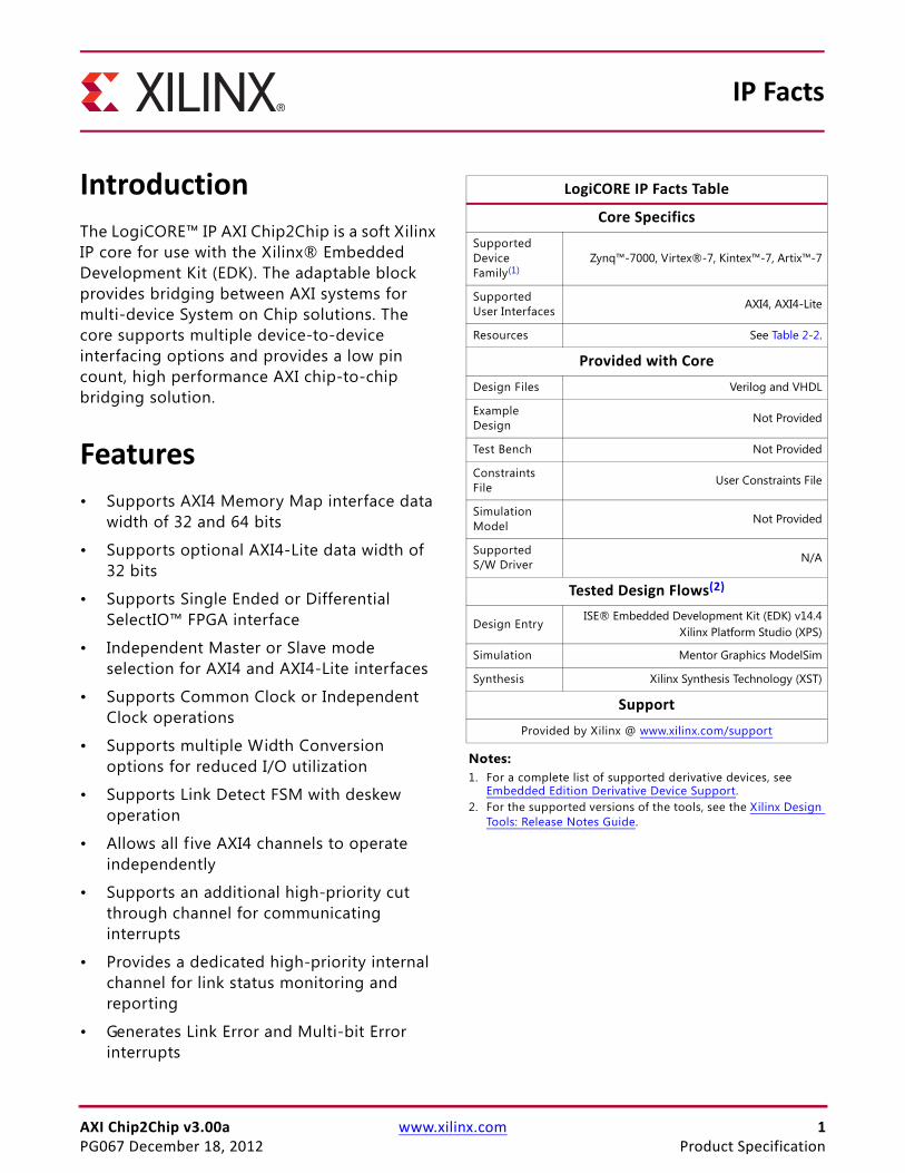
IntroductionThe LogiCORE™ IP AXI Chip2Chip is a soft Xilinx IP core for use with the Xilinx® Embedded Development Kit (EDK). The adaptable block provides bridging between AXI systems for multi-device System on Chip solutions. The core supports multiple device-to-device interfacing options and provides a low pin count, high performance AXI chip-to-chip bridging solution.
Features• Supports AXI4 Memory Map interface data
width of 32 and 64 bits
• Supports optional AXI4-Lite data width of 32 bits
• Supports Single Ended or Differential SelectIO™ FPGA interface
• Independent Master or Slave mode selection for AXI4 and AXI4-Lite interfaces
• Supports Common Clock or Independent Clock operations
• Supports multiple Width Conversion options for reduced I/O utilization
• Supports Link Detect FSM with deskew operation
• Allows all f ive AXI4 channels to operate independently
• Supports an additional high-priority cut through channel for communicating interrupts
• Provides a dedicated high-priority internal channel for link status monitoring and reporting
• Generates Link Error and Multi-bit Error interrupts
IP Facts
LogiCORE IP Facts Table
Core SpecificsSupported Device Family(1)
Zynq™-7000, Virtex®-7, Kintex™-7, Artix™-7
Supported User Interfaces AXI4, AXI4-Lite
Resources See Table 2-2.
Provided with CoreDesign Files Verilog and VHDL
Example Design Not Provided
Test Bench Not Provided
Constraints File User Constraints File
Simulation Model Not Provided
Supported S/W Driver N/A
Tested Design Flows(2)
Design EntryISE® Embedded Development Kit (EDK) v14.4
Xilinx Platform Studio (XPS)
Simulation Mentor Graphics ModelSim
Synthesis Xilinx Synthesis Technology (XST)
SupportProvided by Xilinx @ www.xilinx.com/support
Notes: 1. For a complete list of supported derivative devices, see
Embedded Edition Derivative Device Support.2. For the supported versions of the tools, see the Xilinx Design
Tools: Release Notes Guide.
AXI Chip2Chip v3.00a www.xilinx.com 1PG067 December 18, 2012
Chapter 1
OverviewThe LogiCORE™ IP AXI Chip2Chip core functions like a bridge to seamlessly connect two devices over an AXI interface. The core transparently bridges transactions in compliance with AXI protocol specif ications. The bridging function allows all AXI channels to operate independently by forwarding per-channel data and control information in compliance with AXI per-channel Valid-Ready handshake.
The optional AXI4-Lite functions in the core are independent of AXI4 Interface functions. The AXI4-Lite interface can be used for low-bandwidth access such as configuration/status registers of a peripheral Master.
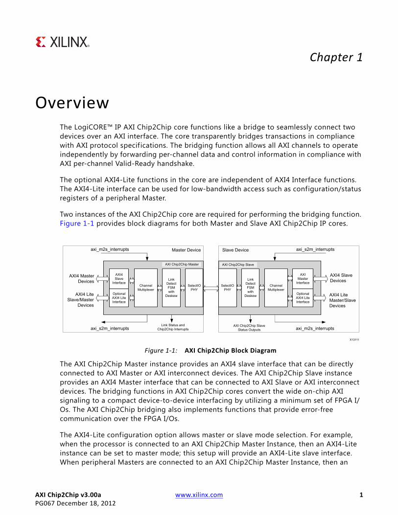
Two instances of the AXI Chip2Chip core are required for performing the bridging function. Figure 1-1 provides block diagrams for both Master and Slave AXI Chip2Chip IP cores.
The AXI Chip2Chip Master instance provides an AXI4 slave interface that can be directly connected to AXI Master or AXI interconnect devices. The AXI Chip2Chip Slave instance provides an AXI4 Master interface that can be connected to AXI Slave or AXI interconnect devices. The bridging functions in AXI Chip2Chip cores convert the wide on-chip AXI signaling to a compact device-to-device interfacing by utilizing a minimum set of FPGA I/Os. The AXI Chip2Chip bridging also implements functions that provide error-free communication over the FPGA I/Os.
The AXI4-Lite configuration option allows master or slave mode selection. For example, when the processor is connected to an AXI Chip2Chip Master Instance, then an AXI4-Lite instance can be set to master mode; this setup will provide an AXI4-Lite slave interface. When peripheral Masters are connected to an AXI Chip2Chip Master Instance, then an
X-Ref Target - Figure 1-1
Figure 1-1: AXI Chip2Chip Block Diagram
AXI Chip2Chip v3.00a www.xilinx.com 2PG067 December 18, 2012
Feature Summary
AXI4-Lite instance can be set to slave mode and it will provide an AXI4-lite master interface. For more details on AXI4-Lite configuration options, see Chip2Chip AXI4-Lite Mode in Chapter 4.
AXI Chip2Chip operations can be categorized into five modules: AXI4 Interface, AXI4-Lite Interface, Channel Multiplexer, Link Detect FSM with deskew, and PHY interface.
Feature SummaryThis section summarizes the functionality of the f ive modules.
AXI4 InterfaceThe AXI Chip2Chip core provides an AXI4 interface to map to AXI Memory Mapped devices in the device fabric. AXI Memory Mapped devices can be AXI Master, AXI interconnect, or AXI Slave functions. The AXI Interface can operate in either Common Clock or in Independent clock modes. For more details on clocking and latencies, see General Design Guidelines in Chapter 3.
TIP: The AXI4 interface of the Chip2Chip core provides WUSER signals to maintain compatibility with AXI3 interface specifications. Any AXI3 master that supports write interleaving can use the AXI4 WUSER[3:0] signals to map the WID[3:0] signals in AXI3 write data channel.
AXI4-Lite InterfaceThe AXI4-Lite functions in the core are implemented with a shared address and data bus approach. This allows AXI4-Lite Master to accept a new write transaction only on completion of previous write transaction. This means it only accepts new writes on receiving a write response from the AXI4-Lite Slave. Similarly, the AXI4-Lite Master accepts a new read transaction only on completion of previous read transaction. This means it only accepts reads after receiving a read response and data from the AXI4-Lite Slave. For more details on the AXI4 Lite clocking and reset, see General Design Guidelines in Chapter 3.
Channel MultiplexerThe Channel Multiplexer multiplexes AXI Address and Data channels over FPGA I/Os. In addition, the AXI Chip2Chip core internally determines a 2:1 or 4:1 width conversion based on the Chip2Chip PHY Width option selected for the cores. Width conversion is used for reduced I/O utilization between the two devices. For more details on width conversion, see Chip2Chip PHY Width in Chapter 4.
The Channel Multiplexer also multiplexes AXI, AXI4-Lite and interrupt interfaces over the same set of FPGA I/Os. The priority round-robin multiplexing in the Chip2Chip core assigns
AXI Chip2Chip v3.00a www.xilinx.com 3PG067 December 18, 2012
Feature Summary
the highest priority to interrupt signals, second highest priority to the low-bandwidth AXI4-Lite interface, and last priority to the AXI interface. The priority round-robin multiplexing is in effect when more than one of these interfaces are active simultaneously.
Link Detect FSM with DeskewThe Link Detect FSM with deskew operation ensures that the AXI Chip2Chip Master core initiates transactions only when both Master and Slave cores are out of reset and deskew patterns are exchanged without any bit errors. Deskew operations align data until an optimized sampling point is determined for the data. The nibble level deskew operation also enhances the maximum frequency of operation for the SelectIO™ interface. For more details on Link Detect FSM and deskew operations, see Calibration and Link Error Detection in Chapter 3.
SelectIO PHY InterfaceThe AXI Chip2Chip core provides the SelectIO FPGA interface as an interfacing option between the devices. The SelectIO provides minimum latency between the devices and provides SDR or DDR operations. When the SelectIO interface is used, the I/O type and I/O location must be specif ied in the user constraints f ile (System UCF file).
Interrupt SignalsThe AXI Chip2Chip core allows level interrupts to be communicated through a high-priority internal channel. Interrupts can be independently communicated between AXI Masters and AXI Slaves. On detecting a value change in the interrupt inputs, the AXI Chip2Chip Master core initiates a high-priority transfer to update the interrupt outputs of the AXI Chip2Chip Slave core. Similarly, on detecting a value change in the interrupt inputs, the AXI Chip2Chip Slave core initiates a high-priority transfer to update the interrupt outputs of the AXI Chip2Chip Master core.
The AXI Chip2Chip Master core also generates interrupts for link error conditions. Interrupt signals are asserted by the AXI Chip2Chip Master core. For this, the error conditions detected in the AXI Chip2Chip Slave core are communicated to the Master device through a high-priority internal channel.
The following interrupt signals are supported in the AXI Chip2Chip Master core:
• Link Error Interrupt: Asserted when the AXI Chip2Chip Slave core is reset during normal operation. For more details on Link Error Interrupt, see Resets in Chapter 3.
• Multibit Error Interrupt: When asserted, a Multibit Error interrupt indicates multiple bits are received in error in the Master or Slave AXI Chip2Chip core. For the SelectIO interface, a multibit error is determined during deskew operations and indicates deskew operation failure.
After being asserted, interrupt flags can be cleared only with a reset.
AXI Chip2Chip v3.00a www.xilinx.com 4PG067 December 18, 2012
Applications
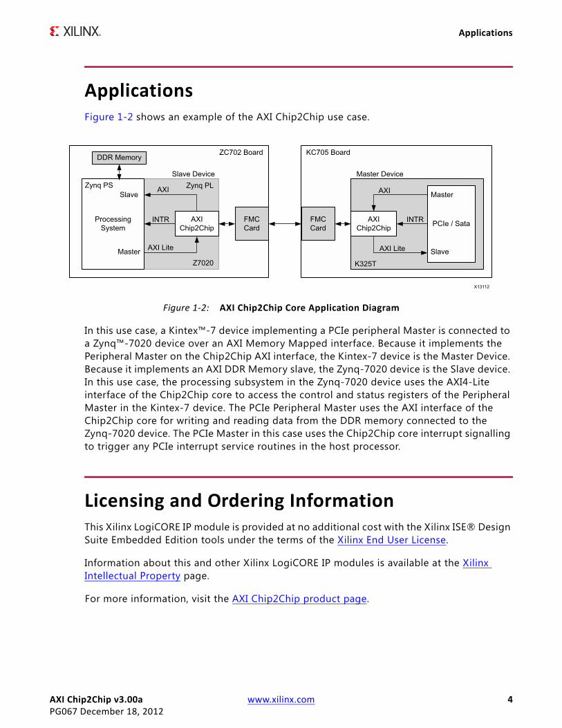
ApplicationsFigure 1-2 shows an example of the AXI Chip2Chip use case.
In this use case, a Kintex™-7 device implementing a PCIe peripheral Master is connected to a Zynq™-7020 device over an AXI Memory Mapped interface. Because it implements the Peripheral Master on the Chip2Chip AXI interface, the Kintex-7 device is the Master Device. Because it implements an AXI DDR Memory slave, the Zynq-7020 device is the Slave device. In this use case, the processing subsystem in the Zynq-7020 device uses the AXI4-Lite interface of the Chip2Chip core to access the control and status registers of the Peripheral Master in the Kintex-7 device. The PCIe Peripheral Master uses the AXI interface of the Chip2Chip core for writing and reading data from the DDR memory connected to the Zynq-7020 device. The PCIe Master in this case uses the Chip2Chip core interrupt signalling to trigger any PCIe interrupt service routines in the host processor.
Licensing and Ordering InformationThis Xilinx LogiCORE IP module is provided at no additional cost with the Xilinx ISE® Design Suite Embedded Edition tools under the terms of the Xilinx End User License.
Information about this and other Xilinx LogiCORE IP modules is available at the Xilinx Intellectual Property page.
For more information, visit the AXI Chip2Chip product page.
X-Ref Target - Figure 1-2
Figure 1-2: AXI Chip2Chip Core Application Diagram
AXI Chip2Chip v3.00a www.xilinx.com 5PG067 December 18, 2012 Product Specification
Chapter 2
Product Specification
Standards ComplianceThis core has bus interfaces that comply with the ARM® AMBA® AXI4 Protocol Specification Version 1.0.
Performance
Maximum FrequenciesThe AXI Chip2Chip core operates up to 200 MHz on Artix-7 devices with -1 and higher speed grades.
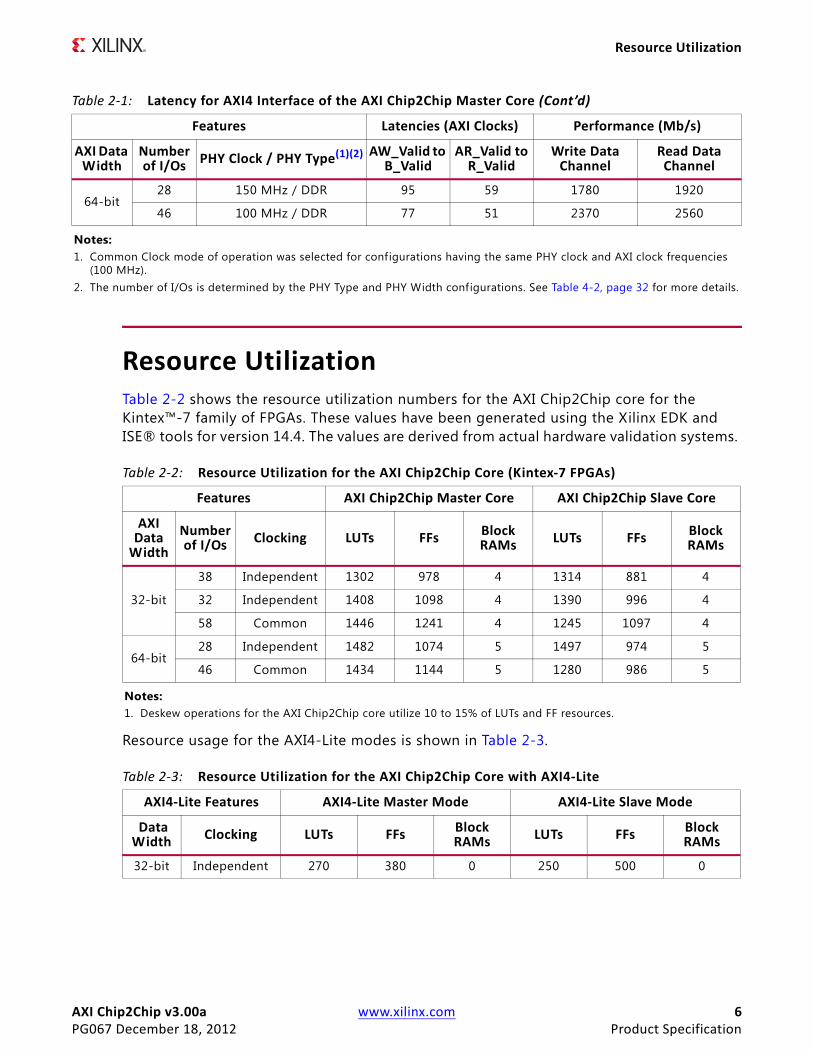
LatencyTable 2-1 lists the latencies and performance measurements on the AXI4 interface of the Chip2Chip Master core. The measurements were taken with simultaneous read and write operations. The measurement setup issued up to four AXI4 outstanding transactions. The AXI (system) clock frequency was set to 100 MHz, and ALEN was set to 16 beats. The measured latency can have up to 5-10% variation and does not account for system latencies outside of the AXI Chip2Chip core.
Table 2-1: Latency for AXI4 Interface of the AXI Chip2Chip Master Core
Features Latencies (AXI Clocks) Performance (Mb/s)
AXI Data Width
Number of I/Os PHY Clock / PHY Type(1)(2) AW_Valid to
B_ValidAR_Valid to
R_ValidWrite Data
ChannelRead Data Channel
32-bit
38 200 MHz / SDR 77 44 1190 1280
32 150 MHz / DDR 69 47 1770 1920
58 100 MHz / DDR 57 42 2350 2550
AXI Chip2Chip v3.00a www.xilinx.com 6PG067 December 18, 2012 Product Specification
Resource Utilization
Resource UtilizationTable 2-2 shows the resource utilization numbers for the AXI Chip2Chip core for the Kintex™-7 family of FPGAs. These values have been generated using the Xilinx EDK and ISE® tools for version 14.4. The values are derived from actual hardware validation systems.
Resource usage for the AXI4-Lite modes is shown in Table 2-3.
64-bit28 150 MHz / DDR 95 59 1780 1920
46 100 MHz / DDR 77 51 2370 2560
Notes: 1. Common Clock mode of operation was selected for configurations having the same PHY clock and AXI clock frequencies
(100 MHz).2. The number of I/Os is determined by the PHY Type and PHY Width configurations. See Table 4-2, page 32 for more details.
Table 2-1: Latency for AXI4 Interface of the AXI Chip2Chip Master Core (Cont’d)
Features Latencies (AXI Clocks) Performance (Mb/s)
AXI Data Width
Number of I/Os PHY Clock / PHY Type(1)(2) AW_Valid to
B_ValidAR_Valid to
R_ValidWrite Data
ChannelRead Data Channel
Table 2-2: Resource Utilization for the AXI Chip2Chip Core (Kintex-7 FPGAs)
Features AXI Chip2Chip Master Core AXI Chip2Chip Slave Core
AXI Data
WidthNumber of I/Os Clocking LUTs FFs Block
RAMs LUTs FFs Block RAMs
32-bit
38 Independent 1302 978 4 1314 881 4
32 Independent 1408 1098 4 1390 996 4
58 Common 1446 1241 4 1245 1097 4
64-bit28 Independent 1482 1074 5 1497 974 5
46 Common 1434 1144 5 1280 986 5
Notes: 1. Deskew operations for the AXI Chip2Chip core utilize 10 to 15% of LUTs and FF resources.
Table 2-3: Resource Utilization for the AXI Chip2Chip Core with AXI4-Lite
AXI4-Lite Features AXI4-Lite Master Mode AXI4-Lite Slave Mode
Data Width Clocking LUTs FFs Block
RAMs LUTs FFs Block RAMs
32-bit Independent 270 380 0 250 500 0
AXI Chip2Chip v3.00a www.xilinx.com 7PG067 December 18, 2012 Product Specification
Port Descriptions
Port DescriptionsThis section provides port descriptions for the AXI Chip2Chip core. It is organized according to Master and Slave ports.
AXI Chip2Chip MasterThis section describes the ports when the AXI Chip2Chip core is a Master. It contains these subsections:
• Global Signals
• AXI Interface Signals
• Master Device Interface Signals
• Interrupt and Status Signals
Global Signals
Table 2-4 describes the global signals for the AXI Chip2Chip Master core.
Table 2-4: Global Interface Signals
Name Direction Description
s_aclk Input Global Slave Interface Clock. For Independent Clock mode, all signals on the AXI Slave interface of an AXI Chip2Chip Master core are synchronous to s_aclk .For Common Clock mode, all AXI Chip2Chip Master core operations are synchronous to s_aclk .
axi_c2c_phy_clk Input Physical Interface Clock. The axi_c2c_phy_clk signal is applicable only when Independent Mode operation is selected for the core. AXI Chip2Chip Master core operations excluding the AXI Slave Interface are synchronous to axi_c2c_phy_clk .
idelay_ref_clk Input SelectIO Interface I/O Reference Clock. This signal is applicable only when the SelectIO interface is selected as the FPGA interfacing option and when deskew is enabled for the SelectIO interface. The applicable frequency for idelay_ref_clk is 200 MHz or 300 MHz (±10 MHz).
s_aresetn Input Global Reset. This signal is active-Low and synchronous. All applicable clock inputs to the AXI Chip2Chip Master core must be stable when s_aresetn input is de-asserted.
Optional AXI4-Lite Signals
AXI Chip2Chip v3.00a www.xilinx.com 8PG067 December 18, 2012 Product Specification
Port Descriptions
AXI Interface Signals
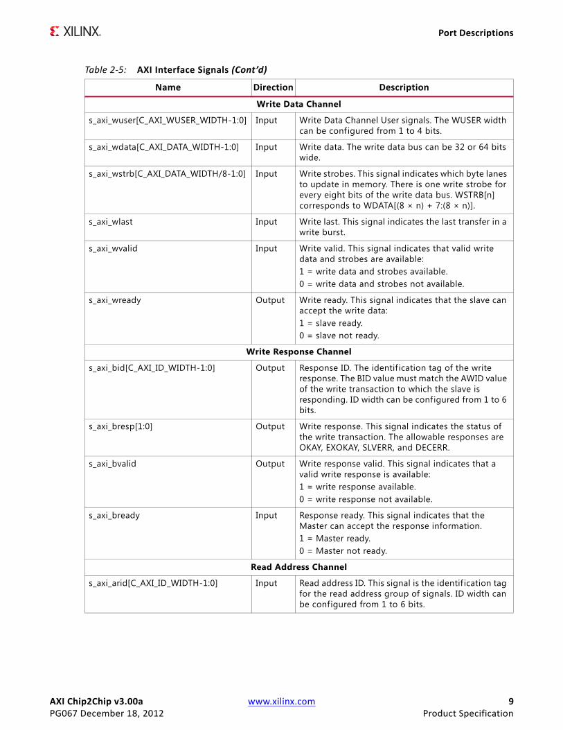
Table 2-5 describes the AXI Interface signals for the AXI Chip2Chip Master core.
m_axi_lite_aclk Input Master Interface AXI4-Lite Clock. Applicable only when Slave Mode of AXI4-Lite is selected. All signals are sampled on the rising edge of this clock.
s_axi_lite_aclk Input Slave Interface AXI4-Lite Clock. Applicable only when Master Mode of AXI-Lite is selected. All signals are sampled on the rising edge of this clock.
Table 2-5: AXI Interface Signals
Name Direction Description
Write Address Channel
s_axi_awid[C_AXI_ID_WIDTH-1:0] Input Write address ID. This signal is the identif ication tag for the write address group of signals. ID width can be configured from 1 to 6 bits.
s_axi_awaddr[31:0] Input Write address. The write address bus gives the address of the f irst transfer in a write burst transaction. The associated control signals are used to determine the addresses of the remaining transfers in the burst.
s_axi_awlen[7:0] Input Burst length. The burst length gives the exact number of transfers in a burst. This information determines the number of data transfers associated with the address.
s_axi_awsize[1:0] Input Burst size. This signal indicates the size of each transfer in the burst. Byte lane strobes indicate exactly which byte lanes to update.
s_axi_awburst[1:0] Input Burst type. The burst type, coupled with the size information, details how the address for each transfer within the burst is calculated.
s_axi_awvalid Input Write address valid. This signal indicates that valid write address and control information are available:1 = address and control information available.0 = address and control information not available.The address and control information remain stable until the address acknowledge signal, AWREADY, goes HIGH
s_axi_awready Output Write address ready. This signal indicates that the slave is ready to accept an address and associated control signals:1 = slave ready0 = slave not ready.
Table 2-4: Global Interface Signals (Cont’d)
Name Direction Description
AXI Chip2Chip v3.00a www.xilinx.com 9PG067 December 18, 2012 Product Specification
Port Descriptions
Write Data Channel
s_axi_wuser[C_AXI_WUSER_WIDTH-1:0] Input Write Data Channel User signals. The WUSER width can be configured from 1 to 4 bits.
s_axi_wdata[C_AXI_DATA_WIDTH-1:0] Input Write data. The write data bus can be 32 or 64 bits wide.
s_axi_wstrb[C_AXI_DATA_WIDTH/8-1:0] Input Write strobes. This signal indicates which byte lanes to update in memory. There is one write strobe for every eight bits of the write data bus. WSTRB[n] corresponds to WDATA[(8 × n) + 7:(8 × n)].
s_axi_wlast Input Write last. This signal indicates the last transfer in a write burst.
s_axi_wvalid Input Write valid. This signal indicates that valid write data and strobes are available:1 = write data and strobes available.0 = write data and strobes not available.
s_axi_wready Output Write ready. This signal indicates that the slave can accept the write data:1 = slave ready.0 = slave not ready.
Write Response Channel
s_axi_bid[C_AXI_ID_WIDTH-1:0] Output Response ID. The identif ication tag of the write response. The BID value must match the AWID value of the write transaction to which the slave is responding. ID width can be configured from 1 to 6 bits.
s_axi_bresp[1:0] Output Write response. This signal indicates the status of the write transaction. The allowable responses are OKAY, EXOKAY, SLVERR, and DECERR.
s_axi_bvalid Output Write response valid. This signal indicates that a valid write response is available:1 = write response available.0 = write response not available.
s_axi_bready Input Response ready. This signal indicates that the Master can accept the response information.1 = Master ready.0 = Master not ready.
Read Address Channel
s_axi_arid[C_AXI_ID_WIDTH-1:0] Input Read address ID. This signal is the identif ication tag for the read address group of signals. ID width can be configured from 1 to 6 bits.
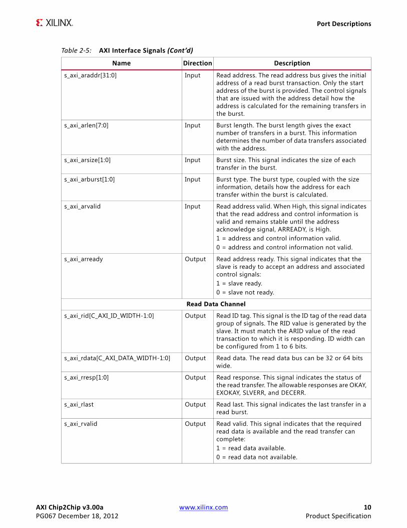
Table 2-5: AXI Interface Signals (Cont’d)
Name Direction Description
AXI Chip2Chip v3.00a www.xilinx.com 10PG067 December 18, 2012 Product Specification
Port Descriptions
s_axi_araddr[31:0] Input Read address. The read address bus gives the initial address of a read burst transaction. Only the start address of the burst is provided. The control signals that are issued with the address detail how the address is calculated for the remaining transfers in the burst.
s_axi_arlen[7:0] Input Burst length. The burst length gives the exact number of transfers in a burst. This information determines the number of data transfers associated with the address.
s_axi_arsize[1:0] Input Burst size. This signal indicates the size of each transfer in the burst.
s_axi_arburst[1:0] Input Burst type. The burst type, coupled with the size information, details how the address for each transfer within the burst is calculated.
s_axi_arvalid Input Read address valid. When High, this signal indicates that the read address and control information is valid and remains stable until the address acknowledge signal, ARREADY, is High.1 = address and control information valid.0 = address and control information not valid.
s_axi_arready Output Read address ready. This signal indicates that the slave is ready to accept an address and associated control signals:1 = slave ready.0 = slave not ready.
Read Data Channel
s_axi_rid[C_AXI_ID_WIDTH-1:0] Output Read ID tag. This signal is the ID tag of the read data group of signals. The RID value is generated by the slave. It must match the ARID value of the read transaction to which it is responding. ID width can be configured from 1 to 6 bits.
s_axi_rdata[C_AXI_DATA_WIDTH-1:0] Output Read data. The read data bus can be 32 or 64 bits wide.
s_axi_rresp[1:0] Output Read response. This signal indicates the status of the read transfer. The allowable responses are OKAY, EXOKAY, SLVERR, and DECERR.
s_axi_rlast Output Read last. This signal indicates the last transfer in a read burst.
s_axi_rvalid Output Read valid. This signal indicates that the required read data is available and the read transfer can complete:1 = read data available.0 = read data not available.
Table 2-5: AXI Interface Signals (Cont’d)
Name Direction Description
AXI Chip2Chip v3.00a www.xilinx.com 11PG067 December 18, 2012 Product Specification
Port Descriptions
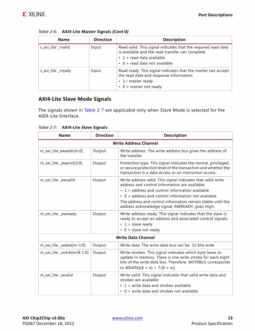
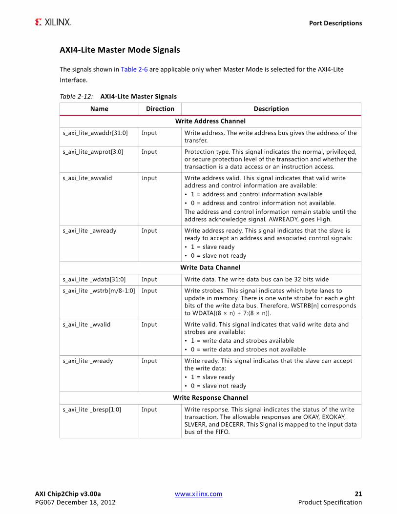
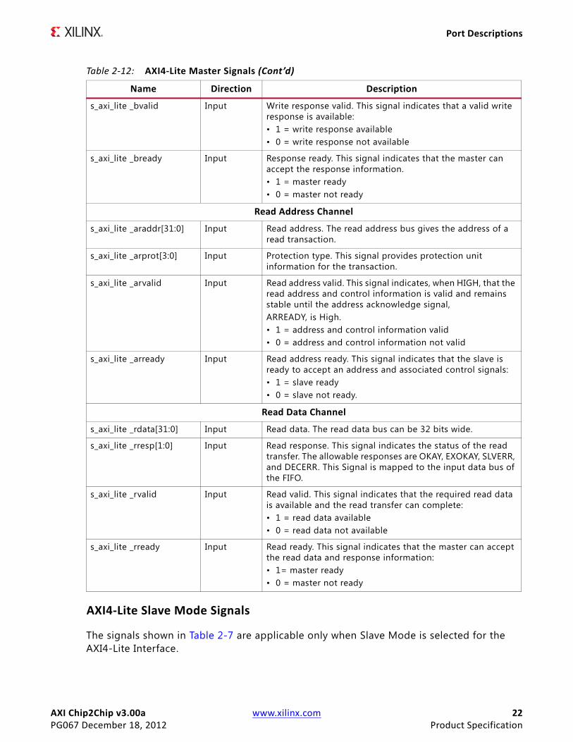
AXI4-Lite Master Mode Signals
The signals shown in Table 2-6 are applicable only when Master Mode is selected for the AXI4-Lite Interface.
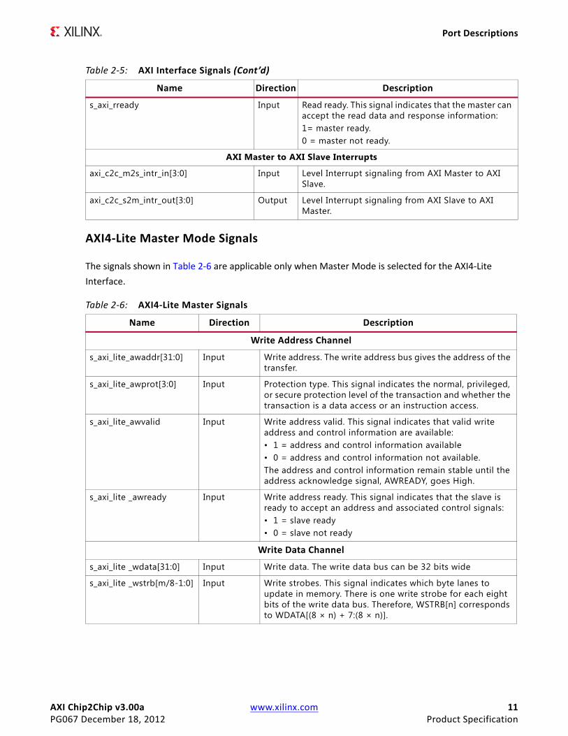
s_axi_rready Input Read ready. This signal indicates that the master can accept the read data and response information:1= master ready.0 = master not ready.
AXI Master to AXI Slave Interrupts
axi_c2c_m2s_intr_in[3:0] Input Level Interrupt signaling from AXI Master to AXI Slave.
axi_c2c_s2m_intr_out[3:0] Output Level Interrupt signaling from AXI Slave to AXI Master.
Table 2-6: AXI4-Lite Master Signals
Name Direction Description
Write Address Channel
s_axi_lite_awaddr[31:0] Input Write address. The write address bus gives the address of the transfer.
s_axi_lite_awprot[3:0] Input Protection type. This signal indicates the normal, privileged, or secure protection level of the transaction and whether the transaction is a data access or an instruction access.
s_axi_lite_awvalid Input Write address valid. This signal indicates that valid write address and control information are available: • 1 = address and control information available • 0 = address and control information not available. The address and control information remain stable until the address acknowledge signal, AWREADY, goes High.
s_axi_lite _awready Input Write address ready. This signal indicates that the slave is ready to accept an address and associated control signals: • 1 = slave ready • 0 = slave not ready
Write Data Channel
s_axi_lite _wdata[31:0] Input Write data. The write data bus can be 32 bits wide
s_axi_lite _wstrb[m/8-1:0] Input Write strobes. This signal indicates which byte lanes to update in memory. There is one write strobe for each eight bits of the write data bus. Therefore, WSTRB[n] corresponds to WDATA[(8 × n) + 7:(8 × n)].
Table 2-5: AXI Interface Signals (Cont’d)
Name Direction Description
AXI Chip2Chip v3.00a www.xilinx.com 12PG067 December 18, 2012 Product Specification
Port Descriptions
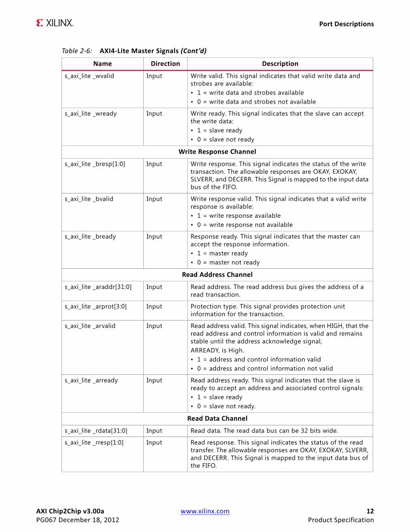
s_axi_lite _wvalid Input Write valid. This signal indicates that valid write data and strobes are available: • 1 = write data and strobes available • 0 = write data and strobes not available
s_axi_lite _wready Input Write ready. This signal indicates that the slave can accept the write data: • 1 = slave ready • 0 = slave not ready
Write Response Channel
s_axi_lite _bresp[1:0] Input Write response. This signal indicates the status of the write transaction. The allowable responses are OKAY, EXOKAY, SLVERR, and DECERR. This Signal is mapped to the input data bus of the FIFO.
s_axi_lite _bvalid Input Write response valid. This signal indicates that a valid write response is available: • 1 = write response available • 0 = write response not available
s_axi_lite _bready Input Response ready. This signal indicates that the master can accept the response information.• 1 = master ready • 0 = master not ready
Read Address Channel
s_axi_lite _araddr[31:0] Input Read address. The read address bus gives the address of a read transaction.
s_axi_lite _arprot[3:0] Input Protection type. This signal provides protection unit information for the transaction.
s_axi_lite _arvalid Input Read address valid. This signal indicates, when HIGH, that the read address and control information is valid and remains stable until the address acknowledge signal,ARREADY, is High.• 1 = address and control information valid • 0 = address and control information not valid
s_axi_lite _arready Input Read address ready. This signal indicates that the slave is ready to accept an address and associated control signals: • 1 = slave ready • 0 = slave not ready.
Read Data Channel
s_axi_lite _rdata[31:0] Input Read data. The read data bus can be 32 bits wide.
s_axi_lite _rresp[1:0] Input Read response. This signal indicates the status of the read transfer. The allowable responses are OKAY, EXOKAY, SLVERR, and DECERR. This Signal is mapped to the input data bus of the FIFO.
Table 2-6: AXI4-Lite Master Signals (Cont’d)
Name Direction Description
AXI Chip2Chip v3.00a www.xilinx.com 13PG067 December 18, 2012 Product Specification
Port Descriptions
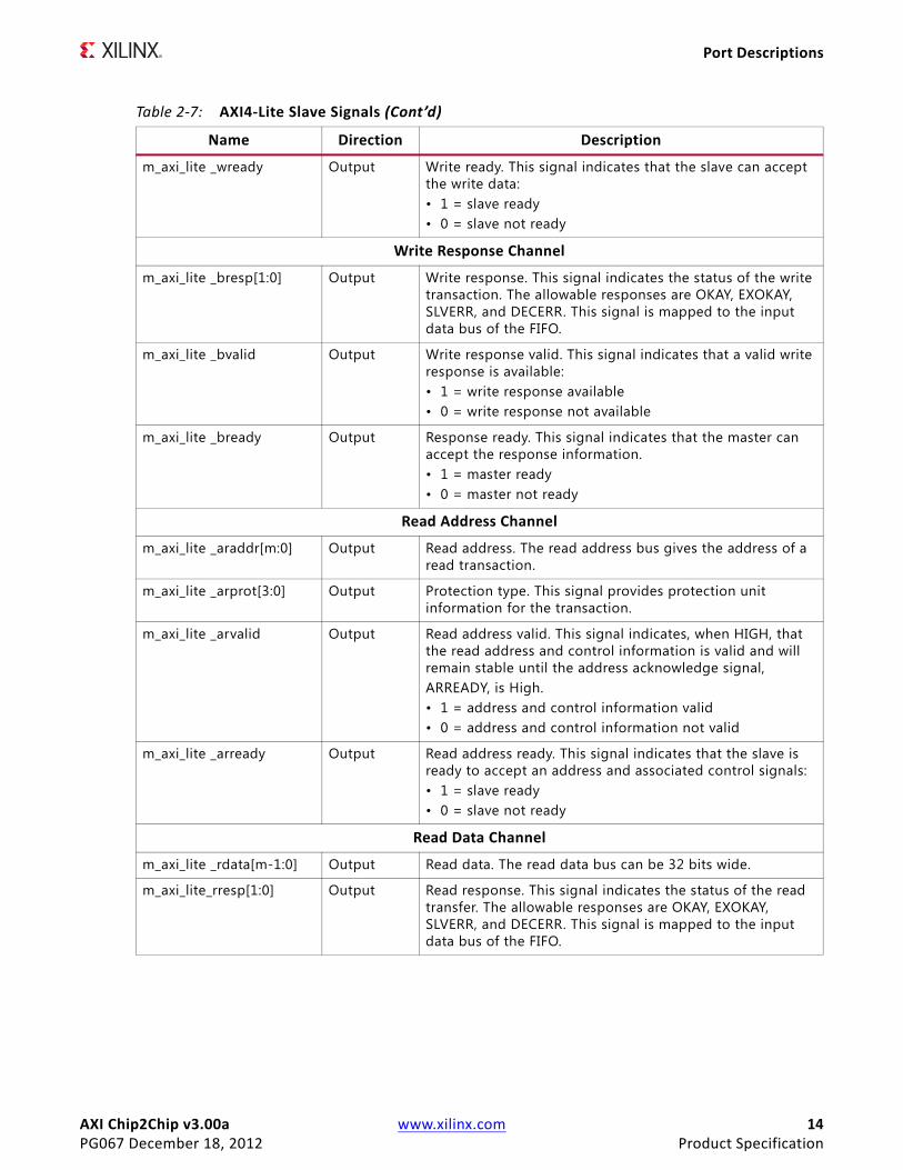
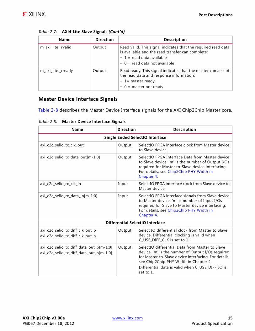
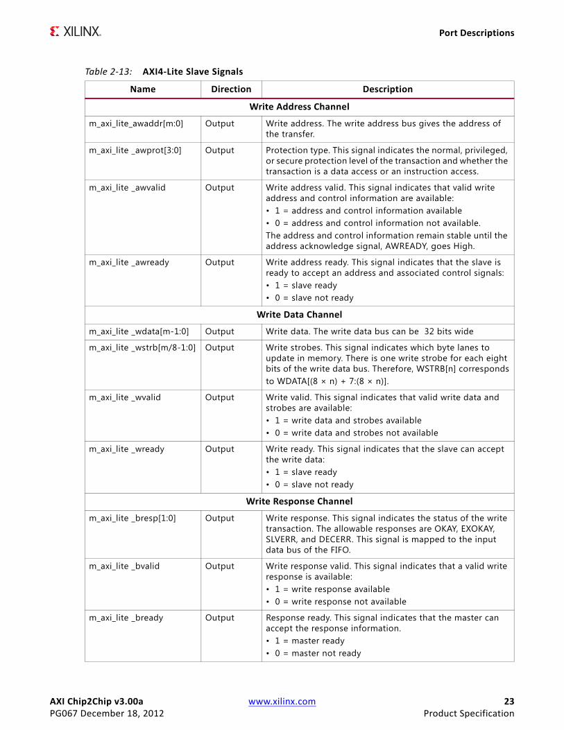
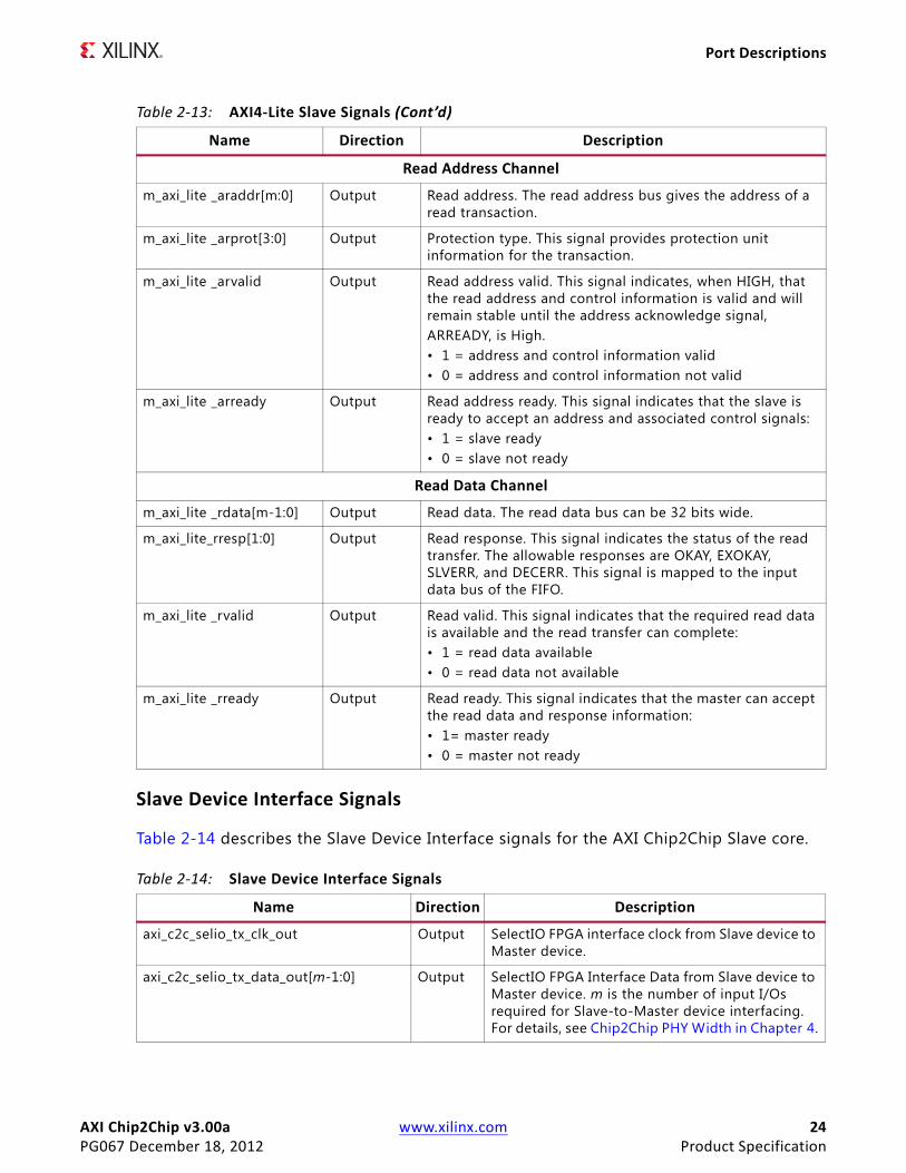
AXI4-Lite Slave Mode Signals
The signals shown in Table 2-7 are applicable only when Slave Mode is selected for the AXI4-Lite Interface.
s_axi_lite _rvalid Input Read valid. This signal indicates that the required read data is available and the read transfer can complete: • 1 = read data available • 0 = read data not available
s_axi_lite _rready Input Read ready. This signal indicates that the master can accept the read data and response information: • 1= master ready • 0 = master not ready
Table 2-7: AXI4-Lite Slave Signals
Name Direction Description
Write Address Channel
m_axi_lite_awaddr[m:0] Output Write address. The write address bus gives the address of the transfer.
m_axi_lite _awprot[3:0] Output Protection type. This signal indicates the normal, privileged, or secure protection level of the transaction and whether the transaction is a data access or an instruction access.
m_axi_lite _awvalid Output Write address valid. This signal indicates that valid write address and control information are available: • 1 = address and control information available • 0 = address and control information not available. The address and control information remain stable until the address acknowledge signal, AWREADY, goes High.
m_axi_lite _awready Output Write address ready. This signal indicates that the slave is ready to accept an address and associated control signals: • 1 = slave ready • 0 = slave not ready
Write Data Channel
m_axi_lite _wdata[m-1:0] Output Write data. The write data bus can be 32 bits wide
m_axi_lite _wstrb[m/8-1:0] Output Write strobes. This signal indicates which byte lanes to update in memory. There is one write strobe for each eight bits of the write data bus. Therefore, WSTRB[n] correspondsto WDATA[(8 × n) + 7:(8 × n)].
m_axi_lite _wvalid Output Write valid. This signal indicates that valid write data and strobes are available: • 1 = write data and strobes available • 0 = write data and strobes not available
Table 2-6: AXI4-Lite Master Signals (Cont’d)
Name Direction Description
AXI Chip2Chip v3.00a www.xilinx.com 14PG067 December 18, 2012 Product Specification
Port Descriptions
m_axi_lite _wready Output Write ready. This signal indicates that the slave can accept the write data: • 1 = slave ready • 0 = slave not ready
Write Response Channel
m_axi_lite _bresp[1:0] Output Write response. This signal indicates the status of the write transaction. The allowable responses are OKAY, EXOKAY, SLVERR, and DECERR. This signal is mapped to the input data bus of the FIFO.
m_axi_lite _bvalid Output Write response valid. This signal indicates that a valid write response is available: • 1 = write response available • 0 = write response not available
m_axi_lite _bready Output Response ready. This signal indicates that the master can accept the response information.• 1 = master ready • 0 = master not ready
Read Address Channel
m_axi_lite _araddr[m:0] Output Read address. The read address bus gives the address of a read transaction.
m_axi_lite _arprot[3:0] Output Protection type. This signal provides protection unit information for the transaction.
m_axi_lite _arvalid Output Read address valid. This signal indicates, when HIGH, that the read address and control information is valid and will remain stable until the address acknowledge signal,ARREADY, is High.• 1 = address and control information valid • 0 = address and control information not valid
m_axi_lite _arready Output Read address ready. This signal indicates that the slave is ready to accept an address and associated control signals: • 1 = slave ready • 0 = slave not ready
Read Data Channel
m_axi_lite _rdata[m-1:0] Output Read data. The read data bus can be 32 bits wide.
m_axi_lite_rresp[1:0] Output Read response. This signal indicates the status of the read transfer. The allowable responses are OKAY, EXOKAY, SLVERR, and DECERR. This signal is mapped to the input data bus of the FIFO.
Table 2-7: AXI4-Lite Slave Signals (Cont’d)
Name Direction Description
AXI Chip2Chip v3.00a www.xilinx.com 15PG067 December 18, 2012 Product Specification
Port Descriptions
Master Device Interface Signals
Table 2-8 describes the Master Device Interface signals for the AXI Chip2Chip Master core.
m_axi_lite _rvalid Output Read valid. This signal indicates that the required read data is available and the read transfer can complete: • 1 = read data available • 0 = read data not available
m_axi_lite _rready Output Read ready. This signal indicates that the master can accept the read data and response information: • 1= master ready • 0 = master not ready
Table 2-8: Master Device Interface Signals
Name Direction Description
Single Ended SelectIO Interface
axi_c2c_selio_tx_clk_out Output SelectIO FPGA interface clock from Master device to Slave device.
axi_c2c_selio_tx_data_out[m-1:0] Output SelectIO FPGA Interface Data from Master device to Slave device. ‘m’ is the number of Output I/Os required for Master-to-Slave device interfacing. For details, see Chip2Chip PHY Width in Chapter 4.
axi_c2c_selio_rx_clk_in Input SelectIO FPGA interface clock from Slave device to Master device.
axi_c2c_selio_rx_data_in[m-1:0] Input SelectIO FPGA interface signals from Slave device to Master device. ‘m’ is number of Input I/Os required for Slave to Master device interfacing. For details, see Chip2Chip PHY Width in Chapter 4.
Differential SelectIO Interface
axi_c2c_selio_tx_diff_clk_out_paxi_c2c_selio_tx_diff_clk_out_n
Output Select IO differential clock from Master to Slave device. Differential clocking is valid when C_USE_DIFF_CLK is set to 1.
axi_c2c_selio_tx_diff_data_out_p[m-1:0]axi_c2c_selio_tx_diff_data_out_n[m-1:0]
Output SelectIO differential Data from Master to Slave device. 'm' is the number of Output I/Os required for Master-to-Slave device interfacing. For details, see Chip2Chip PHY Width in Chapter 4.Differential data is valid when C_USE_DIFF_IO is set to 1.
Table 2-7: AXI4-Lite Slave Signals (Cont’d)
Name Direction Description
AXI Chip2Chip v3.00a www.xilinx.com 16PG067 December 18, 2012 Product Specification
Port Descriptions
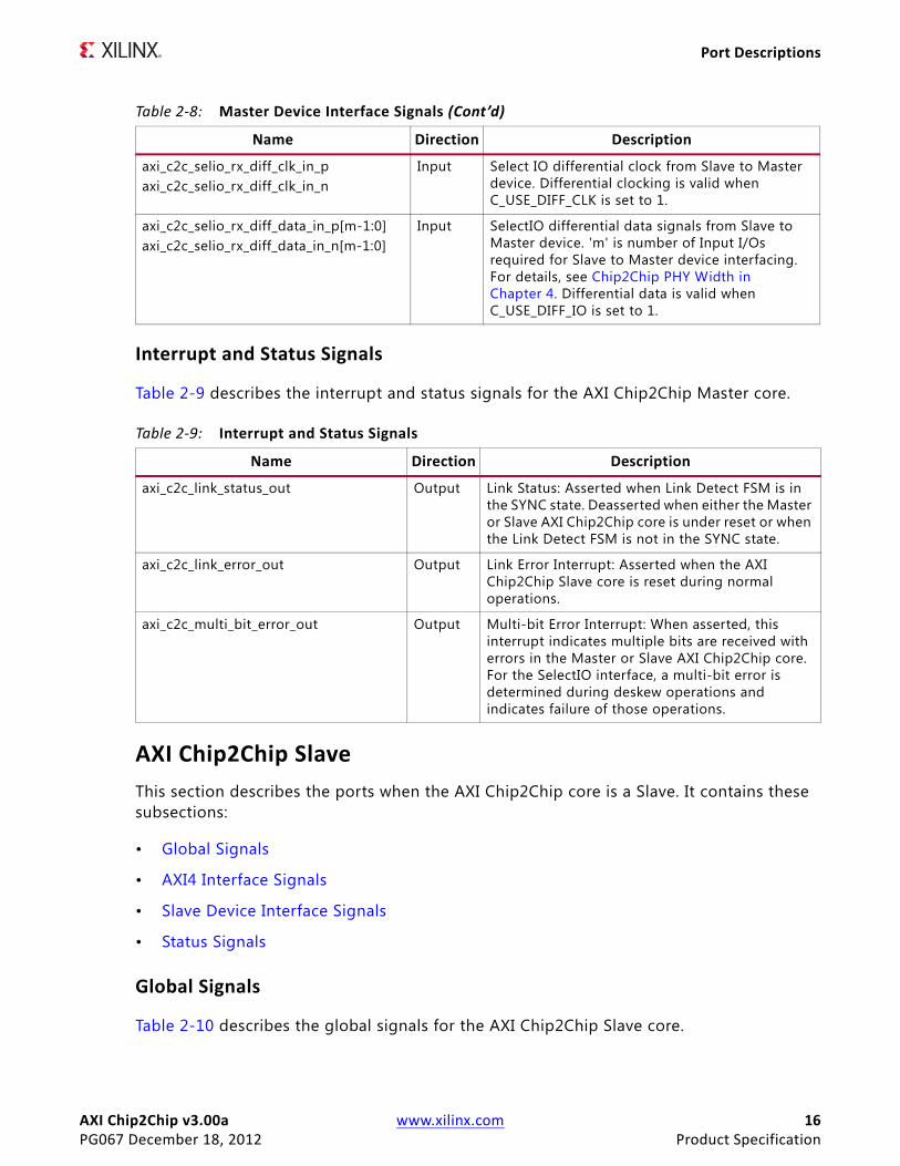
Interrupt and Status Signals
Table 2-9 describes the interrupt and status signals for the AXI Chip2Chip Master core.
AXI Chip2Chip SlaveThis section describes the ports when the AXI Chip2Chip core is a Slave. It contains these subsections:
• Global Signals
• AXI4 Interface Signals
• Slave Device Interface Signals
• Status Signals
Global Signals
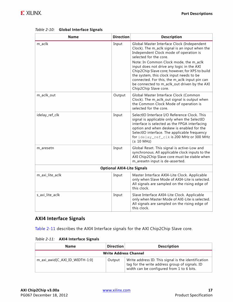
Table 2-10 describes the global signals for the AXI Chip2Chip Slave core.
axi_c2c_selio_rx_diff_clk_in_paxi_c2c_selio_rx_diff_clk_in_n
Input Select IO differential clock from Slave to Master device. Differential clocking is valid when C_USE_DIFF_CLK is set to 1.
axi_c2c_selio_rx_diff_data_in_p[m-1:0]axi_c2c_selio_rx_diff_data_in_n[m-1:0]
Input SelectIO differential data signals from Slave to Master device. 'm' is number of Input I/Os required for Slave to Master device interfacing. For details, see Chip2Chip PHY Width in Chapter 4. Differential data is valid when C_USE_DIFF_IO is set to 1.
Table 2-9: Interrupt and Status Signals
Name Direction Description
axi_c2c_link_status_out Output Link Status: Asserted when Link Detect FSM is in the SYNC state. Deasserted when either the Master or Slave AXI Chip2Chip core is under reset or when the Link Detect FSM is not in the SYNC state.
axi_c2c_link_error_out Output Link Error Interrupt: Asserted when the AXI Chip2Chip Slave core is reset during normal operations.
axi_c2c_multi_bit_error_out Output Multi-bit Error Interrupt: When asserted, this interrupt indicates multiple bits are received with errors in the Master or Slave AXI Chip2Chip core. For the SelectIO interface, a multi-bit error is determined during deskew operations and indicates failure of those operations.
Table 2-8: Master Device Interface Signals (Cont’d)
Name Direction Description
AXI Chip2Chip v3.00a www.xilinx.com 17PG067 December 18, 2012 Product Specification
Port Descriptions
AXI4 Interface Signals
Table 2-11 describes the AXI4 Interface signals for the AXI Chip2Chip Slave core.
Table 2-10: Global Interface Signals
Name Direction Description
m_aclk Input Global Master Interface Clock (Independent Clock). The m_aclk signal is an input when the Independent Clock mode of operation is selected for the core.Note: In Common Clock mode, the m_aclk input does not drive any logic in the AXI Chip2Chip Slave core; however, for XPS to build the system, this clock input needs to be connected. For this, the m_aclk input pin can be connected to m_aclk_out driven by the AXI Chip2Chip Slave core.
m_aclk_out Output Global Master Interface Clock (Common Clock). The m_aclk_out signal is output when the Common Clock Mode of operation is selected for the core.
idelay_ref_clk Input SelectIO Interface I/O Reference Clock. This signal is applicable only when the SelectIO interface is selected as the FPGA interfacing option and when deskew is enabled for the SelectIO interface. The applicable frequency for idelay_ref_clk is 200 MHz or 300 MHz (± 10 MHz)
m_aresetn Input Global Reset. This signal is active-Low and synchronous. All applicable clock inputs to the AXI Chip2Chip Slave core must be stable when m_aresetn input is de-asserted.
Optional AXI4-Lite Signals
m_axi_lite_aclk Input Master Interface AXI4-Lite Clock. Applicable only when Slave Mode of AXI4-Lite is selected. All signals are sampled on the rising edge of this clock.
s_axi_lite_aclk Input Slave Interface AXI4-Lite Clock. Applicable only when Master Mode of AXI-Lite is selected. All signals are sampled on the rising edge of this clock.
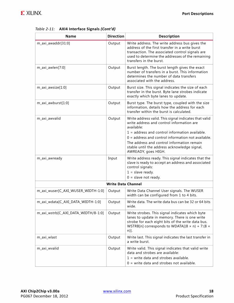
Table 2-11: AXI4 Interface Signals
Name Direction Description
Write Address Channel
m_axi_awid[C_AXI_ID_WIDTH-1:0] Output Write address ID. This signal is the identif ication tag for the write address group of signals. ID width can be configured from 1 to 6 bits.
AXI Chip2Chip v3.00a www.xilinx.com 18PG067 December 18, 2012 Product Specification
Port Descriptions
m_axi_awaddr[31:0] Output Write address. The write address bus gives the address of the f irst transfer in a write burst transaction. The associated control signals are used to determine the addresses of the remaining transfers in the burst.
m_axi_awlen[7:0] Output Burst length. The burst length gives the exact number of transfers in a burst. This information determines the number of data transfers associated with the address.
m_axi_awsize[1:0] Output Burst size. This signal indicates the size of each transfer in the burst. Byte lane strobes indicate exactly which byte lanes to update.
m_axi_awburst[1:0] Output Burst type. The burst type, coupled with the size information, details how the address for each transfer within the burst is calculated.
m_axi_awvalid Output Write address valid. This signal indicates that valid write address and control information are available:1 = address and control information available.0 = address and control information not available.The address and control information remain stable until the address acknowledge signal, AWREADY, goes HIGH.
m_axi_awready Input Write address ready. This signal indicates that the slave is ready to accept an address and associated control signals:1 = slave ready.0 = slave not ready.
Write Data Channel
m_axi_wuser[C_AXI_WUSER_WIDTH-1:0] Output Write Data Channel User signals. The WUSER width can be configured from 1 to 4 bits.
m_axi_wdata[C_AXI_DATA_WIDTH-1:0] Output Write data. The write data bus can be 32 or 64 bits wide.
m_axi_wstrb[C_AXI_DATA_WIDTH/8-1:0] Output Write strobes. This signal indicates which byte lanes to update in memory. There is one write strobe for each eight bits of the write data bus. WSTRB[n] corresponds to WDATA[(8 × n) + 7:(8 × n)].
m_axi_wlast Output Write last. This signal indicates the last transfer in a write burst.
m_axi_wvalid Output Write valid. This signal indicates that valid write data and strobes are available:1 = write data and strobes available.0 = write data and strobes not available.
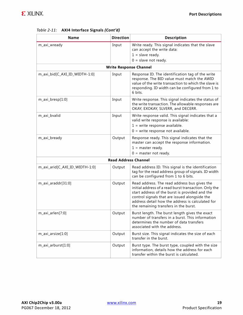
Table 2-11: AXI4 Interface Signals (Cont’d)
Name Direction Description
AXI Chip2Chip v3.00a www.xilinx.com 19PG067 December 18, 2012 Product Specification
Port Descriptions
m_axi_wready Input Write ready. This signal indicates that the slave can accept the write data:1 = slave ready.0 = slave not ready.
Write Response Channel
m_axi_bid[C_AXI_ID_WIDTH-1:0] Input Response ID. The identif ication tag of the write response. The BID value must match the AWID value of the write transaction to which the slave is responding. ID width can be configured from 1 to 6 bits.
m_axi_bresp[1:0] Input Write response. This signal indicates the status of the write transaction. The allowable responses are OKAY, EXOKAY, SLVERR, and DECERR.
m_axi_bvalid Input Write response valid. This signal indicates that a valid write response is available:1 = write response available.0 = write response not available.
m_axi_bready Output Response ready. This signal indicates that the master can accept the response information.1 = master ready.0 = master not ready.
Read Address Channel
m_axi_arid[C_AXI_ID_WIDTH-1:0] Output Read address ID. This signal is the identif ication tag for the read address group of signals. ID width can be configured from 1 to 6 bits.
m_axi_araddr[31:0] Output Read address. The read address bus gives the initial address of a read burst transaction. Only the start address of the burst is provided and the control signals that are issued alongside the address detail how the address is calculated for the remaining transfers in the burst.
m_axi_arlen[7:0] Output Burst length. The burst length gives the exact number of transfers in a burst. This information determines the number of data transfers associated with the address.
m_axi_arsize[1:0] Output Burst size. This signal indicates the size of each transfer in the burst.
m_axi_arburst[1:0] Output Burst type. The burst type, coupled with the size information, details how the address for each transfer within the burst is calculated.
Table 2-11: AXI4 Interface Signals (Cont’d)
Name Direction Description
AXI Chip2Chip v3.00a www.xilinx.com 20PG067 December 18, 2012 Product Specification
Port Descriptions
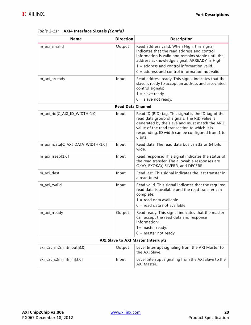
m_axi_arvalid Output Read address valid. When High, this signal indicates that the read address and control information is valid and remains stable until the address acknowledge signal, ARREADY, is High.1 = address and control information valid.0 = address and control information not valid.
m_axi_arready Input Read address ready. This signal indicates that the slave is ready to accept an address and associated control signals:1 = slave ready.0 = slave not ready.
Read Data Channel
m_axi_rid[C_AXI_ID_WIDTH-1:0] Input Read ID (RID) tag. This signal is the ID tag of the read data group of signals. The RID value is generated by the slave and must match the ARID value of the read transaction to which it is responding. ID width can be configured from 1 to 6 bits.
m_axi_rdata[C_AXI_DATA_WIDTH-1:0] Input Read data. The read data bus can 32 or 64 bits wide.
m_axi_rresp[1:0] Input Read response. This signal indicates the status of the read transfer. The allowable responses are OKAY, EXOKAY, SLVERR, and DECERR.
m_axi_rlast Input Read last. This signal indicates the last transfer in a read burst.
m_axi_rvalid Input Read valid. This signal indicates that the required read data is available and the read transfer can complete:1 = read data available.0 = read data not available.
m_axi_rready Output Read ready. This signal indicates that the master can accept the read data and response information:1= master ready.0 = master not ready.
AXI Slave to AXI Master Interrupts
axi_c2c_m2s_intr_out[3:0] Output Level Interrupt signaling from the AXI Master to the AXI Slave.
axi_c2c_s2m_intr_in[3:0] Input Level Interrupt signaling from the AXI Slave to the AXI Master.
Table 2-11: AXI4 Interface Signals (Cont’d)
Name Direction Description
AXI Chip2Chip v3.00a www.xilinx.com 21PG067 December 18, 2012 Product Specification
Port Descriptions
AXI4-Lite Master Mode Signals
The signals shown in Table 2-6 are applicable only when Master Mode is selected for the AXI4-Lite Interface.
Table 2-12: AXI4-Lite Master Signals
Name Direction Description
Write Address Channel
s_axi_lite_awaddr[31:0] Input Write address. The write address bus gives the address of the transfer.
s_axi_lite_awprot[3:0] Input Protection type. This signal indicates the normal, privileged, or secure protection level of the transaction and whether the transaction is a data access or an instruction access.
s_axi_lite_awvalid Input Write address valid. This signal indicates that valid write address and control information are available: • 1 = address and control information available • 0 = address and control information not available. The address and control information remain stable until the address acknowledge signal, AWREADY, goes High.
s_axi_lite _awready Input Write address ready. This signal indicates that the slave is ready to accept an address and associated control signals: • 1 = slave ready • 0 = slave not ready
Write Data Channel
s_axi_lite _wdata[31:0] Input Write data. The write data bus can be 32 bits wide
s_axi_lite _wstrb[m/8-1:0] Input Write strobes. This signal indicates which byte lanes to update in memory. There is one write strobe for each eight bits of the write data bus. Therefore, WSTRB[n] corresponds to WDATA[(8 × n) + 7:(8 × n)].
s_axi_lite _wvalid Input Write valid. This signal indicates that valid write data and strobes are available: • 1 = write data and strobes available • 0 = write data and strobes not available
s_axi_lite _wready Input Write ready. This signal indicates that the slave can accept the write data: • 1 = slave ready • 0 = slave not ready
Write Response Channel
s_axi_lite _bresp[1:0] Input Write response. This signal indicates the status of the write transaction. The allowable responses are OKAY, EXOKAY, SLVERR, and DECERR. This Signal is mapped to the input data bus of the FIFO.
AXI Chip2Chip v3.00a www.xilinx.com 22PG067 December 18, 2012 Product Specification
Port Descriptions
AXI4-Lite Slave Mode Signals
The signals shown in Table 2-7 are applicable only when Slave Mode is selected for the AXI4-Lite Interface.
s_axi_lite _bvalid Input Write response valid. This signal indicates that a valid write response is available: • 1 = write response available • 0 = write response not available
s_axi_lite _bready Input Response ready. This signal indicates that the master can accept the response information.• 1 = master ready • 0 = master not ready
Read Address Channel
s_axi_lite _araddr[31:0] Input Read address. The read address bus gives the address of a read transaction.
s_axi_lite _arprot[3:0] Input Protection type. This signal provides protection unit information for the transaction.
s_axi_lite _arvalid Input Read address valid. This signal indicates, when HIGH, that the read address and control information is valid and remains stable until the address acknowledge signal,ARREADY, is High.• 1 = address and control information valid • 0 = address and control information not valid
s_axi_lite _arready Input Read address ready. This signal indicates that the slave is ready to accept an address and associated control signals: • 1 = slave ready • 0 = slave not ready.
Read Data Channel
s_axi_lite _rdata[31:0] Input Read data. The read data bus can be 32 bits wide.
s_axi_lite _rresp[1:0] Input Read response. This signal indicates the status of the read transfer. The allowable responses are OKAY, EXOKAY, SLVERR, and DECERR. This Signal is mapped to the input data bus of the FIFO.
s_axi_lite _rvalid Input Read valid. This signal indicates that the required read data is available and the read transfer can complete: • 1 = read data available • 0 = read data not available
s_axi_lite _rready Input Read ready. This signal indicates that the master can accept the read data and response information: • 1= master ready • 0 = master not ready
Table 2-12: AXI4-Lite Master Signals (Cont’d)
Name Direction Description
AXI Chip2Chip v3.00a www.xilinx.com 23PG067 December 18, 2012 Product Specification
Port Descriptions
Table 2-13: AXI4-Lite Slave Signals
Name Direction Description
Write Address Channel
m_axi_lite_awaddr[m:0] Output Write address. The write address bus gives the address of the transfer.
m_axi_lite _awprot[3:0] Output Protection type. This signal indicates the normal, privileged, or secure protection level of the transaction and whether the transaction is a data access or an instruction access.
m_axi_lite _awvalid Output Write address valid. This signal indicates that valid write address and control information are available: • 1 = address and control information available • 0 = address and control information not available. The address and control information remain stable until the address acknowledge signal, AWREADY, goes High.
m_axi_lite _awready Output Write address ready. This signal indicates that the slave is ready to accept an address and associated control signals: • 1 = slave ready • 0 = slave not ready
Write Data Channel
m_axi_lite _wdata[m-1:0] Output Write data. The write data bus can be 32 bits wide
m_axi_lite _wstrb[m/8-1:0] Output Write strobes. This signal indicates which byte lanes to update in memory. There is one write strobe for each eight bits of the write data bus. Therefore, WSTRB[n] correspondsto WDATA[(8 × n) + 7:(8 × n)].
m_axi_lite _wvalid Output Write valid. This signal indicates that valid write data and strobes are available: • 1 = write data and strobes available • 0 = write data and strobes not available
m_axi_lite _wready Output Write ready. This signal indicates that the slave can accept the write data: • 1 = slave ready • 0 = slave not ready
Write Response Channel
m_axi_lite _bresp[1:0] Output Write response. This signal indicates the status of the write transaction. The allowable responses are OKAY, EXOKAY, SLVERR, and DECERR. This signal is mapped to the input data bus of the FIFO.
m_axi_lite _bvalid Output Write response valid. This signal indicates that a valid write response is available: • 1 = write response available • 0 = write response not available
m_axi_lite _bready Output Response ready. This signal indicates that the master can accept the response information.• 1 = master ready • 0 = master not ready
AXI Chip2Chip v3.00a www.xilinx.com 24PG067 December 18, 2012 Product Specification
Port Descriptions
Slave Device Interface Signals
Table 2-14 describes the Slave Device Interface signals for the AXI Chip2Chip Slave core.
Read Address Channel
m_axi_lite _araddr[m:0] Output Read address. The read address bus gives the address of a read transaction.
m_axi_lite _arprot[3:0] Output Protection type. This signal provides protection unit information for the transaction.
m_axi_lite _arvalid Output Read address valid. This signal indicates, when HIGH, that the read address and control information is valid and will remain stable until the address acknowledge signal,ARREADY, is High.• 1 = address and control information valid • 0 = address and control information not valid
m_axi_lite _arready Output Read address ready. This signal indicates that the slave is ready to accept an address and associated control signals: • 1 = slave ready • 0 = slave not ready
Read Data Channel
m_axi_lite _rdata[m-1:0] Output Read data. The read data bus can be 32 bits wide.
m_axi_lite_rresp[1:0] Output Read response. This signal indicates the status of the read transfer. The allowable responses are OKAY, EXOKAY, SLVERR, and DECERR. This signal is mapped to the input data bus of the FIFO.
m_axi_lite _rvalid Output Read valid. This signal indicates that the required read data is available and the read transfer can complete: • 1 = read data available • 0 = read data not available
m_axi_lite _rready Output Read ready. This signal indicates that the master can accept the read data and response information: • 1= master ready • 0 = master not ready
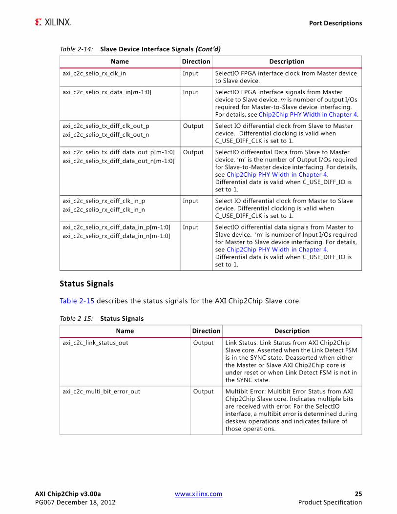
Table 2-14: Slave Device Interface Signals
Name Direction Description
axi_c2c_selio_tx_clk_out Output SelectIO FPGA interface clock from Slave device to Master device.
axi_c2c_selio_tx_data_out[m-1:0] Output SelectIO FPGA Interface Data from Slave device to Master device. m is the number of input I/Os required for Slave-to-Master device interfacing. For details, see Chip2Chip PHY Width in Chapter 4.
Table 2-13: AXI4-Lite Slave Signals (Cont’d)
Name Direction Description
AXI Chip2Chip v3.00a www.xilinx.com 25PG067 December 18, 2012 Product Specification
Port Descriptions
Status Signals
Table 2-15 describes the status signals for the AXI Chip2Chip Slave core.
axi_c2c_selio_rx_clk_in Input SelectIO FPGA interface clock from Master device to Slave device.
axi_c2c_selio_rx_data_in[m-1:0] Input SelectIO FPGA interface signals from Master device to Slave device. m is number of output I/Os required for Master-to-Slave device interfacing. For details, see Chip2Chip PHY Width in Chapter 4.
axi_c2c_selio_tx_diff_clk_out_paxi_c2c_selio_tx_diff_clk_out_n
Output Select IO differential clock from Slave to Master device. Differential clocking is valid when C_USE_DIFF_CLK is set to 1.
axi_c2c_selio_tx_diff_data_out_p[m-1:0]axi_c2c_selio_tx_diff_data_out_n[m-1:0]
Output SelectIO differential Data from Slave to Master device. ‘m’ is the number of Output I/Os required for Slave-to-Master device interfacing. For details, see Chip2Chip PHY Width in Chapter 4. Differential data is valid when C_USE_DIFF_IO is set to 1.
axi_c2c_selio_rx_diff_clk_in_paxi_c2c_selio_rx_diff_clk_in_n
Input Select IO differential clock from Master to Slave device. Differential clocking is valid when C_USE_DIFF_CLK is set to 1.
axi_c2c_selio_rx_diff_data_in_p[m-1:0]axi_c2c_selio_rx_diff_data_in_n[m-1:0]
Input SelectIO differential data signals from Master to Slave device. ‘m’ is number of Input I/Os required for Master to Slave device interfacing. For details, see Chip2Chip PHY Width in Chapter 4. Differential data is valid when C_USE_DIFF_IO is set to 1.
Table 2-15: Status Signals
Name Direction Description
axi_c2c_link_status_out Output Link Status: Link Status from AXI Chip2Chip Slave core. Asserted when the Link Detect FSM is in the SYNC state. Deasserted when either the Master or Slave AXI Chip2Chip core is under reset or when Link Detect FSM is not in the SYNC state.
axi_c2c_multi_bit_error_out Output Multibit Error: Multibit Error Status from AXI Chip2Chip Slave core. Indicates multiple bits are received with error. For the SelectIO interface, a multibit error is determined during deskew operations and indicates failure of those operations.
Table 2-14: Slave Device Interface Signals (Cont’d)
Name Direction Description
AXI Chip2Chip v3.00a www.xilinx.com 26PG067 December 18, 2012
Chapter 3
Designing with the CoreThis chapter includes guidelines and additional information to make designing with the core easier.
General Design GuidelinesThe customizable AXI Chip2Chip core provides multiple clocking and I/O interface options to the user. Users can determine the frequency at which the interface needs to be operated. Based on the interface frequency, the user can select the I/O type by providing the appropriate constraints in the user constraints f ile (UCF). Selecting the SelectIO™ interface DDR option doubles the I/O speed without impacting the latency or performance. Based on the Chip2Chip PHY Width selection, additional internal width conversion stages can be enabled. Each 2:1 stage of width conversion can increase bridging latencies and can also impact performance.
In addition, common clock and independent clock operations can be selected by the user. The common clock mode of operation reduces clock domain crossing latencies, and the independent clock mode provides additional clock conversion functionality. Both AXI Chip2Chip Master and AXI Chip2Chip Slave cores can be independently selected for either Common Clock or Independent clock operation. Operating the AXI Chip2Chip core at frequencies greater than AXI interface frequencies (Independent clock operation) reduces the bridging latencies and can improve overall performance of the AXI Chip2Chip bridging function.
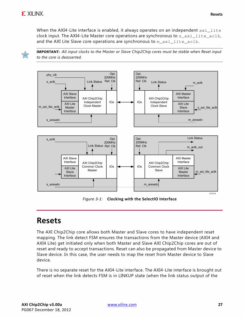
ClockingFigure 3-1 provides the clocking requirement for the SelectIO interface. In addition to AXI clocks, the deskew function, when enabled, requires an additional 200 MHz or 300 MHz (± 10 MHz) reference clock. Both AXI Chip2Chip Master and AXI Chip2Chip Slave cores can be independently selected for either Common Clock or Independent Clock operations. When the AXI Chip2Chip Slave core is selected for Common Clock operation, the core provides clock and reset (Link Status) to the interfacing slave device.
AXI Chip2Chip v3.00a www.xilinx.com 27PG067 December 18, 2012
Resets
When the AXI4-Lite interface is enabled, it always operates on an independent axi_lite clock input. The AXI4-Lite Master core operations are synchronous to s_axi_lite_aclk , and the AXI Lite Slave core operations are synchronous to m_axi_lite_aclk .
IMPORTANT: All input clocks to the Master or Slave Chip2Chip cores must be stable when Reset input to the core is deasserted.
ResetsThe AXI Chip2Chip core allows both Master and Slave cores to have independent reset mapping. The link detect FSM ensures the transactions from the Master device (AXI4 and AXI4 Lite) get initiated only when both Master and Slave AXI Chip2Chip cores are out of reset and ready to accept transactions. Reset can also be propagated from Master device to Slave device. In this case, the user needs to map the reset from Master device to Slave device.
There is no separate reset for the AXI4-Lite interface. The AXI4-Lite interface is brought out of reset when the link detects FSM is in LINKUP state (when the link status output of the
X-Ref Target - Figure 3-1
Figure 3-1: Clocking with the SelectIO Interface
AXI Chip2Chip v3.00a www.xilinx.com 28PG067 December 18, 2012
Calibration and Link Error Detection
core is asserted). All input clocks to the core, including AXI4-Lite clock, must be stable when the core is brought out of reset (when aresetn core input is deasserted).
It is not recommended to reset either Master or Slave AXI Chip2Chip core during normal operation or when Link Status is asserted. AXI Chip2Chip cores maintain a dedicated channel to communicate the Reset condition during normal operations. When the Slave device is reset during normal operations, the Link Status is deasserted and a link error interrupt is asserted.
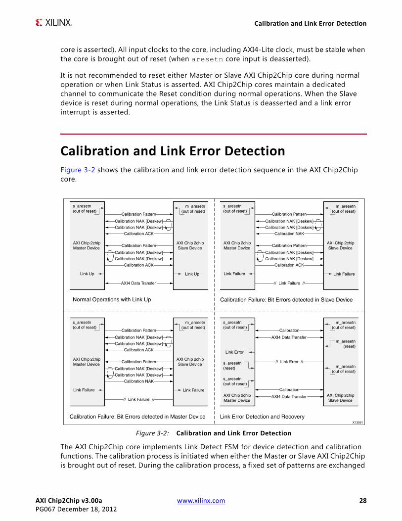
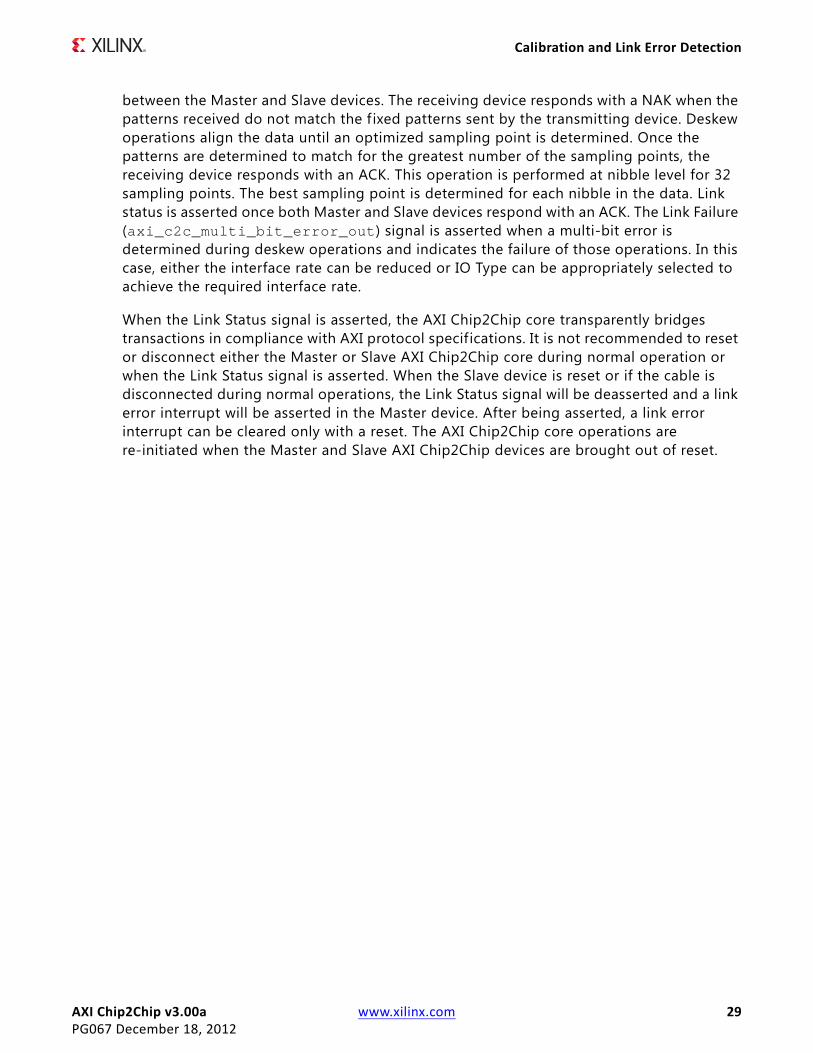
Calibration and Link Error DetectionFigure 3-2 shows the calibration and link error detection sequence in the AXI Chip2Chip core.
The AXI Chip2Chip core implements Link Detect FSM for device detection and calibration functions. The calibration process is initiated when either the Master or Slave AXI Chip2Chip is brought out of reset. During the calibration process, a f ixed set of patterns are exchanged
X-Ref Target - Figure 3-2
Figure 3-2: Calibration and Link Error Detection
AXI Chip2Chip v3.00a www.xilinx.com 29PG067 December 18, 2012
Calibration and Link Error Detection
between the Master and Slave devices. The receiving device responds with a NAK when the patterns received do not match the f ixed patterns sent by the transmitting device. Deskew operations align the data until an optimized sampling point is determined. Once the patterns are determined to match for the greatest number of the sampling points, the receiving device responds with an ACK. This operation is performed at nibble level for 32 sampling points. The best sampling point is determined for each nibble in the data. Link status is asserted once both Master and Slave devices respond with an ACK. The Link Failure (axi_c2c_multi_bit_error_out) signal is asserted when a multi-bit error is determined during deskew operations and indicates the failure of those operations. In this case, either the interface rate can be reduced or IO Type can be appropriately selected to achieve the required interface rate.
When the Link Status signal is asserted, the AXI Chip2Chip core transparently bridges transactions in compliance with AXI protocol specifications. It is not recommended to reset or disconnect either the Master or Slave AXI Chip2Chip core during normal operation or when the Link Status signal is asserted. When the Slave device is reset or if the cable is disconnected during normal operations, the Link Status signal will be deasserted and a link error interrupt will be asserted in the Master device. After being asserted, a link error interrupt can be cleared only with a reset. The AXI Chip2Chip core operations are re-initiated when the Master and Slave AXI Chip2Chip devices are brought out of reset.
AXI Chip2Chip v3.00a www.xilinx.com 30PG067 December 18, 2012
Chapter 4
Customizing and Generating the CoreThis chapter contains information and instructions for using the Xilinx® Embedded Development Kit (EDK) system to customize the LogiCORE™ IP AXI Chip2Chip core.
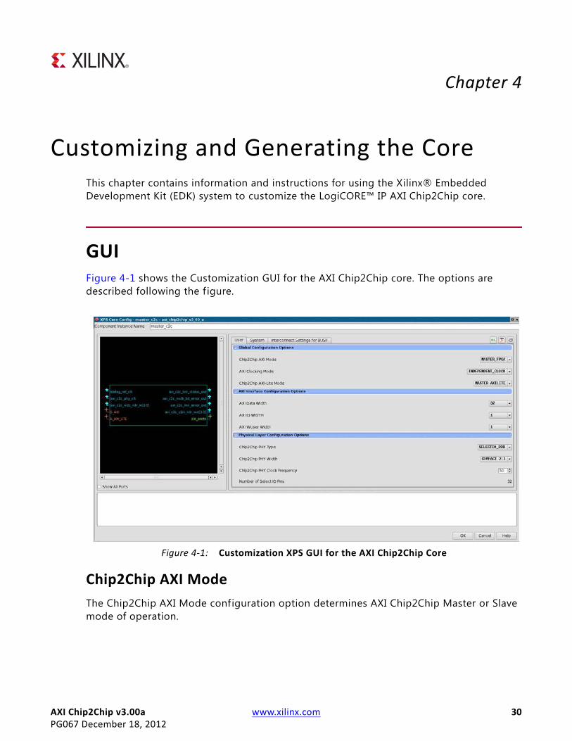
GUIFigure 4-1 shows the Customization GUI for the AXI Chip2Chip core. The options are described following the f igure.
Chip2Chip AXI ModeThe Chip2Chip AXI Mode configuration option determines AXI Chip2Chip Master or Slave mode of operation.
X-Ref Target - Figure 4-1
Figure 4-1: Customization XPS GUI for the AXI Chip2Chip Core
AXI Chip2Chip v3.00a www.xilinx.com 31PG067 December 18, 2012
GUI
AXI Clocking ModeThe AXI Chip2Chip core can be configured with either Independent or Common Clock domains.
The Independent Clock configuration allows you to implement unique clock domains on the AXI interface and FPGA I/Os. The AXI Chip2Chip core handles the synchronization between clock domains. Both the AXI interface and FPGA I/Os can also be maintained in a single clock domain. The AXI Chip2Chip core can be used to generate a core optimized for a single clock by selecting the Common Clock option.
Chip2Chip AXI4-Lite ModeThe Chip2Chip AXI4-Lite Mode configuration option determines AXI4-Lite Master or Slave mode of operation, as shown in Table 4-1. When AXI4-Lite interfacing is not required, this configuration option should be set to “None.”
AXI Data WidthThe AXI Data Width user option allows the width of AXI data to be configured. Valid settings for the AXI Data Width are 32 and 64.
AXI ID WidthThe AXI ID provides an identif ication tag for the group of signals in the channel. AXI ID is supported for all write and read channels. ID width can be configured from 1 to 6 bits.
Note: The AXI ID Width of the AXI Chip2Chip Slave core should match the AXI ID Width of the AXI Chip2Chip Master core.
AXI WUSER WidthAXI WUSER defines sideband information that can be transmitted with the write data channel. The valid range for WUSER width is from 1 to 4 bits.
Table 4-1: AXI4-Lite Configuration Options
Chip2Chip Mode Chip2Chip AXI4-Lite Options
Mode AXI4 Interface Mode AXI4-Lite Interface
Master FPGA Slave
Master Slave
Slave Master
None None
Slave FPGA Master
Master Slave
Slave Master
None None
AXI Chip2Chip v3.00a www.xilinx.com 32PG067 December 18, 2012
Parameter Values in the XCO File
Chip2Chip PHY TypeThe Chip2Chip PHY type can be set to either “SelectIO SDR” or “SelectIO DDR.”
Chip2Chip PHY WidthThe Chip2Chip PHY Width configuration determines I/Os used for device-to-device interfacing. Table 4-2 provides the mapping between Chip2Chip PHY width and the number of input and output I/Os utilized with the selected option.
Chip2Chip PHY FrequencyThe Chip2Chip PHY implements the mixed-mode clock manager (MMCM) on the PHY input clocks. MMCMs are used for clock phase alignment, clock slew reduction, and for compensating clock buffer delays. For common clock AXI Chip2Chip Slave operations, the m_aclk_out output is generated from the MMCM. The Chip2Chip PHY Frequency provides the clock frequency parameter to the MMCM.
Parameter Values in the XCO FileTable 4-3 defines the generic parameters from the XCO file.
IMPORTANT: AXI Chip2chip parameters can be changed by modifying the MHS file.
Table 4-2: FPGA I/O Utilization
AXI Data Width
Chip2ChipPHY Type(1)
Chip2ChipPHY Width
Number ofOutput I/Os
Number ofInput I/Os
32
SelectIO SDRCompact 4:1(2) 19 19
Compact 2:1 31 31
SelectIO DDR
Compact 4:1(2) 10 10
Compact 2:1 16 16
Compact 1:1 29 29
64
SelectIO SDRCompact 4:1(2) 26 26
Compact 2:1 45 45
SelectIO DDR
Compact 4:1(2) 14 14
Compact 2:1 23 23
Compact 1:1 42 421. SelectIO PHY interface routes the clock with the data pins. 2. Compact 4:1 is not supported when the AXI4-Lite Interface is enabled for the core.
AXI Chip2Chip v3.00a www.xilinx.com 33PG067 December 18, 2012
Parameter Values in the XCO File
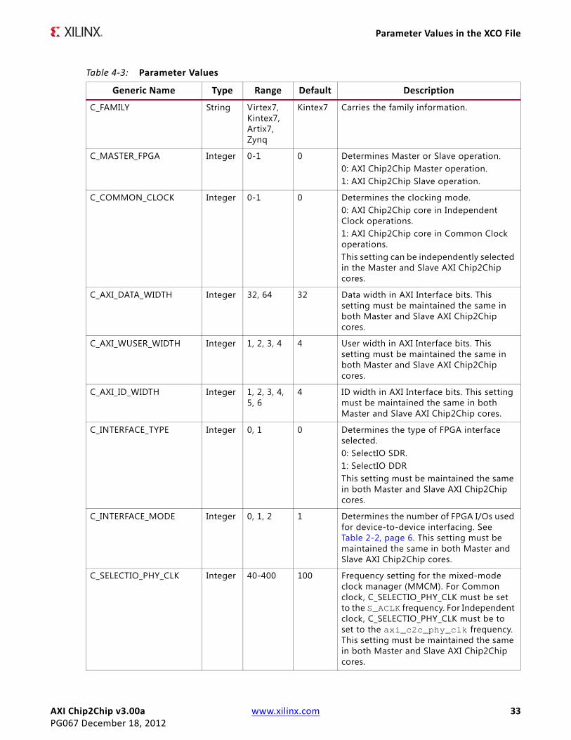
Table 4-3: Parameter Values
Generic Name Type Range Default Description
C_FAMILY String Virtex7, Kintex7, Artix7, Zynq
Kintex7 Carries the family information.
C_MASTER_FPGA Integer 0-1 0 Determines Master or Slave operation.0: AXI Chip2Chip Master operation.1: AXI Chip2Chip Slave operation.
C_COMMON_CLOCK Integer 0-1 0 Determines the clocking mode.0: AXI Chip2Chip core in Independent Clock operations.1: AXI Chip2Chip core in Common Clock operations.This setting can be independently selected in the Master and Slave AXI Chip2Chip cores.
C_AXI_DATA_WIDTH Integer 32, 64 32 Data width in AXI Interface bits. This setting must be maintained the same in both Master and Slave AXI Chip2Chip cores.
C_AXI_WUSER_WIDTH Integer 1, 2, 3, 4 4 User width in AXI Interface bits. This setting must be maintained the same in both Master and Slave AXI Chip2Chip cores.
C_AXI_ID_WIDTH Integer 1, 2, 3, 4, 5, 6
4 ID width in AXI Interface bits. This setting must be maintained the same in both Master and Slave AXI Chip2Chip cores.
C_INTERFACE_TYPE Integer 0, 1 0 Determines the type of FPGA interface selected.0: SelectIO SDR.1: SelectIO DDRThis setting must be maintained the same in both Master and Slave AXI Chip2Chip cores.
C_INTERFACE_MODE Integer 0, 1, 2 1 Determines the number of FPGA I/Os used for device-to-device interfacing. See Table 2-2, page 6. This setting must be maintained the same in both Master and Slave AXI Chip2Chip cores.
C_SELECTIO_PHY_CLK Integer 40-400 100 Frequency setting for the mixed-mode clock manager (MMCM). For Common clock, C_SELECTIO_PHY_CLK must be set to the S_ACLK frequency. For Independent clock, C_SELECTIO_PHY_CLK must be to set to the axi_c2c_phy_clk frequency. This setting must be maintained the same in both Master and Slave AXI Chip2Chip cores.
AXI Chip2Chip v3.00a www.xilinx.com 34PG067 December 18, 2012
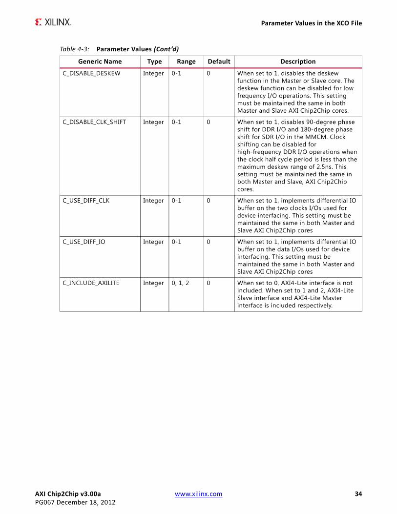
Parameter Values in the XCO File
C_DISABLE_DESKEW Integer 0-1 0 When set to 1, disables the deskew function in the Master or Slave core. The deskew function can be disabled for low frequency I/O operations. This setting must be maintained the same in both Master and Slave AXI Chip2Chip cores.
C_DISABLE_CLK_SHIFT Integer 0-1 0 When set to 1, disables 90-degree phase shift for DDR I/O and 180-degree phase shift for SDR I/O in the MMCM. Clock shifting can be disabled for high-frequency DDR I/O operations when the clock half cycle period is less than the maximum deskew range of 2.5ns. This setting must be maintained the same in both Master and Slave, AXI Chip2Chip cores.
C_USE_DIFF_CLK Integer 0-1 0 When set to 1, implements differential IO buffer on the two clocks I/Os used for device interfacing. This setting must be maintained the same in both Master and Slave AXI Chip2Chip cores
C_USE_DIFF_IO Integer 0-1 0 When set to 1, implements differential IO buffer on the data I/Os used for device interfacing. This setting must be maintained the same in both Master and Slave AXI Chip2Chip cores
C_INCLUDE_AXILITE Integer 0, 1, 2 0 When set to 0, AXI4-Lite interface is not included. When set to 1 and 2, AXI4-Lite Slave interface and AXI4-Lite Master interface is included respectively.
Table 4-3: Parameter Values (Cont’d)
Generic Name Type Range Default Description
AXI Chip2Chip v3.00a www.xilinx.com 35PG067 December 18, 2012
Chapter 5
Constraining the Core
Required ConstraintsThe physical layer is a set of SelectIO™ interface pins that carry source synchronous clock with the data pins.
These I/O pins need I/O Location and I/O Standard constraints. These constraints are board specific and needs to be specif ied accordingly in the top-level UCF.
Clock FrequenciesThe recommended frequency for the AXI interface is up to 200 MHz. For the maximum frequency numbers achieved on the SelectIO PHY interface, see Table A-1 in Appendix A, Verif ication, Compliance, and Interoperability. The clocking mode for the AXI Chip2Chip core needs to be set based on the AXI Interface Frequency and the required SelectIO interface PHY frequency. The required clocking constraints for the AXI Chip2Chip core are listed below:
• s_aclk . The AXI interface of the AXI Chip2Chip Master core operates in the s_aclk clock domain. This clock is constrained by the XPS tool based on the system/interconnect clock wired to this pin.
• axi_c2c_phy_clk . axi_c2c_phy_clk is the SelectIO interface PHY clock and is applicable when the AXI Chip2Chip Master core is configured in Independent Clock mode. For Common Clock mode, this clock constraint is not required because the PHY clock is the same as s_aclk. This clock is constrained by the XPS tool based on the clock wired to this pin.
• m_aclk . The AXI interface of the AXI Chip2Chip Slave core operates in the m_aclk clock domain. This clock is constrained by the XPS tool based on the system/interconnect clock wired to this pin. When the core is configured in Common Clock mode, this constraint is not required because the AXI interface runs on the PHY clock. For more details, see Clocking in Chapter 3.
AXI Chip2Chip v3.00a www.xilinx.com 36PG067 December 18, 2012
Clock Management
• s_axi_lite_aclk . AXI4-Lite Master Mode operates in the s_axi_lite_aclk clock domain. This clock is constrained by the XPS tool based on the system/interconnect clock wired to this pin.
• m_axi_lite_aclk . AXI4-Lite Slave Mode operates in the m_axi_lite_aclk clock domain. This clock is constrained by the XPS tool based on the system/interconnect clock wired to this pin.
• idelay_ref_clk . Both the master and slave AXI Chip2Chip cores utilize the IDELAY_CTRL block for calibration. The idelay_ref_clk input is the reference clock to the IDELAY_CTRL block. This clock is 200 MHz or 300 MHz (± 10MHz) based on the selected device. This constraint is not required when deskew operation is disabled for the cores. The XPS tool generates the constraint for this clock pin based on the clock wired to it.
• axi_c2c_selio_rx_clk_in. axi_c2c_selio_rx_clk_in is the source synchronous clock of the physical layer. This clock pin must be constrained with the PHY clock frequency. When Common Clocking mode is used, this clock runs at the same frequency as s_aclk.
Clock ManagementThe AXI Chip2Chip core utilizes the MMCM module to recover the PHY clock. The frequency of the PHY clock is specif ied by setting the C_SELECTIO_PHY_CLK parameter.
Clock PlacementThe clock input pins on the physical layer must be placed on clock-capable I/Os only.
BankingDevice-specif ic banking rules for placement of PHY I/O pins need to be considered when specifying the top-level UCF.
I/O Standard and PlacementThe I/O pins of the AXI Chip2Chip core need I/O Location and I/O Standard constraints. These constraints need to be specif ied in the top-level UCF.
AXI Chip2Chip v3.00a www.xilinx.com 37PG067 December 18, 2012
Appendix A
Verification, Compliance, and Interoperability
This appendix includes information about how the IP was tested for compliance with the protocol to which it was designed.
SimulationAXI Chip2Chip cores have been tested with Xilinx® ISE® software v14.2 and the Mentor Graphics ModelSim simulator. For the supported versions of these tools, see the Xilinx Design Tools: Release Notes Guide.
The IP is tested using Xilinx proprietary standard AXI Memory Mapped OVM Verif ication Components (OVCs).
Hardware TestingFigure A-1 shows the hardware testing setup for the AXI Chip2Chip core.
AXI Chip2Chip v3.00a www.xilinx.com 38PG067 December 18, 2012
Hardware Testing
The AXI Chip2Chip core has been hardware validated on a KC705 board using a Kintex™-7 FPGA with -1 speed grade (325T). The setup uses two additional FMC loopback cards. Table A-1 provides configuration details for the AXI Chip2Chip core and the frequency achieved by utilizing this setup.
X-Ref Target - Figure A-1
Figure A-1: AXI Chip2Chip Hardware Testing Setup
Table A-1: Hardware Testing Configuration
Features I/Os Utilized PHY Clock (MHz)
AXI Data Width
Chip2ChipPHY Type
Chip2ChipPHY Width
Single Ended [HR I/O Banks]
LVCMOS_25 IO [Unterminated]
32-bit
SelectIO SDR Compact 4:1 38 200
SelectIO DDR Compact 1:1 58 100
SelectIO DDR Compact 2:1 32 150
SelectIO DDR Compact 4:1 20 150
64-bitSelectIO DDR Compact 2:1 46 100
SelectIO DDR Compact 4:1 28 150Note: The AXI (system) clock frequency was set to 100 MHz, and the Common Clock mode of operation was selected for configurations having the same PHY clock and AXI clock frequencies (100 MHz).
AXI Chip2Chip v3.00a www.xilinx.com 39PG067 December 18, 2012
Appendix B
DebuggingThis appendix provides information for using the resources available on the Xilinx Support website, debug tools, and other step-by-step processes for debugging designs that use the AXI Chip2Chip core. It also contains a sample flow diagram and other design samples to guide you through the debug process.
The following topics are included in this appendix:
• Finding Help on Xilinx.com
• Debug Tools
• Simulation Debug
• Hardware Debug
• Interface Debug
Finding Help on Xilinx.comTo help in the design and debug process when using the AXI Chip2Chip core, the Xilinx Support web page (www.xilinx.com/support) contains key resources such as product documentation, release notes, answer records, information about known issues, and links for opening a Technical Support Web Case.
DocumentationThis product guide is the main document associated with the AXI Chip2Chip core. This guide, along with documentation related to all products that aid in the design process, can be found on the Xilinx Support web page (www.xilinx.com/support) or by using the Xilinx Documentation Navigator.
Download the Xilinx Documentation Navigator from the Design Tools tab on the Downloads page (www.xilinx.com/download). For more information about this tool and the features available, open the online help after installation.
AXI Chip2Chip v3.00a www.xilinx.com 40PG067 December 18, 2012
Appendix B: Debugging
Release NotesKnown issues for all cores, including the AXI Chip2Chip core are described in the IP Release Notes Guide (XTP025).
Known IssuesAnswer Records include information about commonly encountered problems, helpful information on how to resolve these problems, and any known issues with a Xilinx product. Answer Records are created and maintained daily ensuring that users have access to the most accurate information available.
Answer Records for this core are listed below, and can also be located by using the Search Support box on the main Xilinx support web page. To maximize your search results, use proper keywords such as:
• Product name
• Tool message(s)
• Summary of the issue encountered
A filter search is available after results are returned to further target the results.
Contacting Technical SupportXilinx provides premier technical support for customers encountering issues that require additional assistance.
To contact Xilinx Technical Support:
1. Navigate to www.xilinx.com/support.
2. Open a WebCase by selecting the WebCase link located under Support Quick Links.
When opening a WebCase, include:
• Target FPGA including package and speed grade.
• All applicable Xilinx Design Tools and simulator software versions.
• Additional f iles based on the specif ic issue might also be required. See the relevant sections in this debug guide for guidelines about which f ile(s) to include with the WebCase.
AXI Chip2Chip v3.00a www.xilinx.com 41PG067 December 18, 2012
Appendix B: Debugging
Debug ToolsThere are many tools available to address AXI Chip2Chip core design issues. It is important to know which tools are useful for debugging various situations.
ChipScope Pro ToolThe ChipScope™ Pro tool inserts logic analyzer, bus analyzer, and virtual I/O cores directly into your design. The ChipScope Pro tool allows you to set trigger conditions to capture application and integrated block port signals in hardware. Captured signals can then be analyzed through the ChipScope Pro Logic Analyzer tool. For detailed information for using the ChipScope Pro tool, see www.xilinx.com/tools/cspro.htm.
Simulation DebugThe simulation debug flow for ModelSim is illustrated below. A similar approach can be used with other simulators.
AXI Chip2Chip v3.00a www.xilinx.com 42PG067 December 18, 2012
Appendix B: Debugging
Hardware DebugHardware issues can range from link bring-up to problems seen after hours of testing. This section provides debug steps for common issues. The ChipScope tool is a valuable resource to use in hardware debug. The signal names mentioned in the following individual sections can be probed using the ChipScope tool for debugging the specif ic problems.
X-Ref Target - Figure B-1
AXI Chip2Chip v3.00a www.xilinx.com 43PG067 December 18, 2012
Appendix B: Debugging
General ChecksEnsure that all the timing constraints for the core were properly incorporated from the example design and that all constraints were met during implementation.
• Does it work in post-place and route timing simulation? If problems are seen in hardware but not in timing simulation, this could indicate a PCB or connector cable issue. Ensure that all clock sources are active and clean.
• If using MMCMs in the design, ensure that all MMCMs have obtained lock by monitoring the LOCKED port.
Interface Debug
AXI4-Lite InterfacesRead from a register that does not have all 0s as a default to verify that the interface is functional. Output s_axi_arready asserts when the read address is valid, and output s_axi_rvalid asserts when the read data/response is valid. If the interface is unresponsive, ensure that the following conditions are met:
• The interface is enabled, and s_axi_lite_aclk/m_axi_lite_aclk are stable when the core is brought out of reset.
• The interface is not being held in reset, and the link status output of the core is asserted.
• The other interface inputs and outputs are connected and toggling.
• The main core clocks are toggling and the link error or multi-bit error interrupt outputs of the core are not asserted.
• If the simulation has been run, verify in simulation and/or a ChipScope tool capture that the waveform is correct for accessing the AXI4-Lite interface.
AXI Chip2Chip v3.00a www.xilinx.com 44PG067 December 18, 2012
Appendix C
Additional Resources
Xilinx ResourcesFor support resources such as Answers, Documentation, Downloads, and Forums, see the Xilinx Support website at:
www.xilinx.com/support.
For a glossary of technical terms used in Xilinx documentation, see:
www.xilinx.com/company/terms.htm.
ReferencesThis section provides supplemental material useful with this product guide:
• AMBA® AXI4 specification
http://infocenter.arm.com/help/index.jsp?topic=/com.arm.doc.ihi0022d/index.html
Technical SupportXilinx provides technical support at www.xilinx.com/support for this LogiCORE™ IP product when used as described in the product documentation. Xilinx cannot guarantee timing, functionality, or support of product if implemented in devices that are not defined in the documentation, if customized beyond that allowed in the product documentation, or if changes are made to any section of the design labeled DO NOT MODIFY.
See the Embedded Edition Derivative Device Support web page (www.xilinx.com/ise/embedded/ddsupport.htm) for a complete list of supported derivative devices for this core.
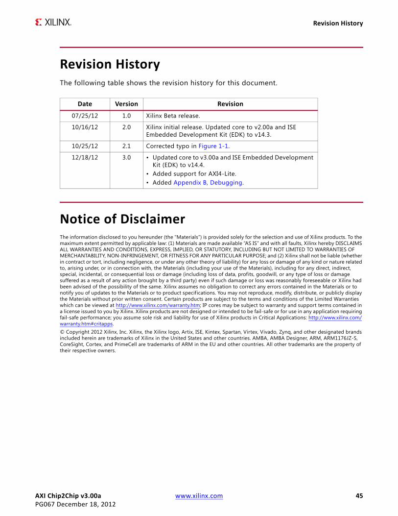
AXI Chip2Chip v3.00a www.xilinx.com 45PG067 December 18, 2012
Revision History
Revision HistoryThe following table shows the revision history for this document.
Notice of DisclaimerThe information disclosed to you hereunder (the “Materials”) is provided solely for the selection and use of Xilinx products. To the maximum extent permitted by applicable law: (1) Materials are made available “AS IS” and with all faults, Xilinx hereby DISCLAIMS ALL WARRANTIES AND CONDITIONS, EXPRESS, IMPLIED, OR STATUTORY, INCLUDING BUT NOT LIMITED TO WARRANTIES OF MERCHANTABILITY, NON-INFRINGEMENT, OR FITNESS FOR ANY PARTICULAR PURPOSE; and (2) Xilinx shall not be liable (whether in contract or tort, including negligence, or under any other theory of liability) for any loss or damage of any kind or nature related to, arising under, or in connection with, the Materials (including your use of the Materials), including for any direct, indirect, special, incidental, or consequential loss or damage (including loss of data, profits, goodwill, or any type of loss or damage suffered as a result of any action brought by a third party) even if such damage or loss was reasonably foreseeable or Xilinx had been advised of the possibility of the same. Xilinx assumes no obligation to correct any errors contained in the Materials or to notify you of updates to the Materials or to product specifications. You may not reproduce, modify, distribute, or publicly display the Materials without prior written consent. Certain products are subject to the terms and conditions of the Limited Warranties which can be viewed at http://www.xilinx.com/warranty.htm; IP cores may be subject to warranty and support terms contained in a license issued to you by Xilinx. Xilinx products are not designed or intended to be fail-safe or for use in any application requiring fail-safe performance; you assume sole risk and liability for use of Xilinx products in Critical Applications: http://www.xilinx.com/warranty.htm#critapps.© Copyright 2012 Xilinx, Inc. Xilinx, the Xilinx logo, Artix, ISE, Kintex, Spartan, Virtex, Vivado, Zynq, and other designated brands included herein are trademarks of Xilinx in the United States and other countries. AMBA, AMBA Designer, ARM, ARM1176JZ-S, CoreSight, Cortex, and PrimeCell are trademarks of ARM in the EU and other countries. All other trademarks are the property of their respective owners.
Date Version Revision
07/25/12 1.0 Xilinx Beta release.
10/16/12 2.0 Xilinx initial release. Updated core to v2.00a and ISE Embedded Development Kit (EDK) to v14.3.
10/25/12 2.1 Corrected typo in Figure 1-1.
12/18/12 3.0 • Updated core to v3.00a and ISE Embedded Development Kit (EDK) to v14.4.
• Added support for AXI4-Lite.• Added Appendix B, Debugging.