Embed Size (px)
Citation preview

LogiCORE IP SPDIF v1.1
Product Guide
PG045 April 24, 2012
LogiCORE IP SPDIF v1.1 www.xilinx.com 2PG045 April 24, 2012
Table of Contents
Chapter 1: OverviewFunctional Description. . . . . . . . . . . . . . . . . . . . . . . . . . . . . . . . . . . . . . . . . . . . . . . . . . . . . . . . . . . . . . 5Feature Summary. . . . . . . . . . . . . . . . . . . . . . . . . . . . . . . . . . . . . . . . . . . . . . . . . . . . . . . . . . . . . . . . . . 6Unsupported Features. . . . . . . . . . . . . . . . . . . . . . . . . . . . . . . . . . . . . . . . . . . . . . . . . . . . . . . . . . . . . . 6Licensing . . . . . . . . . . . . . . . . . . . . . . . . . . . . . . . . . . . . . . . . . . . . . . . . . . . . . . . . . . . . . . . . . . . . . . . . . 7
Chapter 2: Product SpecificationStandards . . . . . . . . . . . . . . . . . . . . . . . . . . . . . . . . . . . . . . . . . . . . . . . . . . . . . . . . . . . . . . . . . . . . . . . . 9Resource Utilization. . . . . . . . . . . . . . . . . . . . . . . . . . . . . . . . . . . . . . . . . . . . . . . . . . . . . . . . . . . . . . . . 9Port Descriptions . . . . . . . . . . . . . . . . . . . . . . . . . . . . . . . . . . . . . . . . . . . . . . . . . . . . . . . . . . . . . . . . . 10Design Parameters . . . . . . . . . . . . . . . . . . . . . . . . . . . . . . . . . . . . . . . . . . . . . . . . . . . . . . . . . . . . . . . . 12Parameter and I/O Signal Dependencies . . . . . . . . . . . . . . . . . . . . . . . . . . . . . . . . . . . . . . . . . . . . . . 14Register Space . . . . . . . . . . . . . . . . . . . . . . . . . . . . . . . . . . . . . . . . . . . . . . . . . . . . . . . . . . . . . . . . . . . 16
Chapter 3: Customizing and Generating the CoreOutput Generation. . . . . . . . . . . . . . . . . . . . . . . . . . . . . . . . . . . . . . . . . . . . . . . . . . . . . . . . . . . . . . . . 26
Chapter 4: Constraining the CoreDevice, Package, and Speed Grade Selections. . . . . . . . . . . . . . . . . . . . . . . . . . . . . . . . . . . . . . . . . . 32Clock Frequencies . . . . . . . . . . . . . . . . . . . . . . . . . . . . . . . . . . . . . . . . . . . . . . . . . . . . . . . . . . . . . . . . 32Clock Placement. . . . . . . . . . . . . . . . . . . . . . . . . . . . . . . . . . . . . . . . . . . . . . . . . . . . . . . . . . . . . . . . . . 33Banking . . . . . . . . . . . . . . . . . . . . . . . . . . . . . . . . . . . . . . . . . . . . . . . . . . . . . . . . . . . . . . . . . . . . . . . . . 33I/O Standard and Placement. . . . . . . . . . . . . . . . . . . . . . . . . . . . . . . . . . . . . . . . . . . . . . . . . . . . . . . . 33
Chapter 5: Designing with the CoreSPDIF Register Module . . . . . . . . . . . . . . . . . . . . . . . . . . . . . . . . . . . . . . . . . . . . . . . . . . . . . . . . . . . . 34
LogiCORE IP SPDIF v1.1 www.xilinx.com 3PG045 April 24, 2012
Chapter 6: Detailed Example DesignExample Design . . . . . . . . . . . . . . . . . . . . . . . . . . . . . . . . . . . . . . . . . . . . . . . . . . . . . . . . . . . . . . . . . . 38Demonstration Test Bench . . . . . . . . . . . . . . . . . . . . . . . . . . . . . . . . . . . . . . . . . . . . . . . . . . . . . . . . . 40
Appendix A: Debugging
Appendix B: Additional ResourcesXilinx Resources . . . . . . . . . . . . . . . . . . . . . . . . . . . . . . . . . . . . . . . . . . . . . . . . . . . . . . . . . . . . . . . . . . 44Solution Centers. . . . . . . . . . . . . . . . . . . . . . . . . . . . . . . . . . . . . . . . . . . . . . . . . . . . . . . . . . . . . . . . . . 44References . . . . . . . . . . . . . . . . . . . . . . . . . . . . . . . . . . . . . . . . . . . . . . . . . . . . . . . . . . . . . . . . . . . . . . 44Technical Support . . . . . . . . . . . . . . . . . . . . . . . . . . . . . . . . . . . . . . . . . . . . . . . . . . . . . . . . . . . . . . . . 45Ordering Information. . . . . . . . . . . . . . . . . . . . . . . . . . . . . . . . . . . . . . . . . . . . . . . . . . . . . . . . . . . . . . 45Revision History . . . . . . . . . . . . . . . . . . . . . . . . . . . . . . . . . . . . . . . . . . . . . . . . . . . . . . . . . . . . . . . . . . 46Notice of Disclaimer. . . . . . . . . . . . . . . . . . . . . . . . . . . . . . . . . . . . . . . . . . . . . . . . . . . . . . . . . . . . . . . 46

LogiCORE IP SPDIF v1.1 www.xilinx.com 4PG045 April 24, 2012 Product Specification
IntroductionThe Sony/Philips Digital Interconnect Format (SPDIF) core is a digital audio interface controller that implements the International Electronic Commission (IEC) 60958-3 interface for transmitting and receiving audio data. This includes standard bus interfaces to the AMBA® AXI4-Lite and AXI4-Stream interfaces, allowing for integration to the IP core with a master system for further processing of audio data. Data collected by the LogiCORE™ IP SPDIF core is stored in the core’s internal FIFO, allowing the system to process a relatively slow audio stream.
FeaturesThe SPDIF soft IP core has these features:
• Configurable as an SPDIF audio data transmitter or an SPDIF audio data receiver
• Configurable FIFO buffer stores the audio sample data
SPDIF Interface• IEC 60958-3 standard SPDIF digital audio bus
interface• Two audio channels• Audio sample lengths of 16/20/24 bits• Data recovery from the bi-phase mark encoded
SPDIF data when the IP core is in receive mode• Variable sampling rates (32 kHz/44.1 kHz/
48 kHz/88.2 kHz/96 kHz/176.4 kHz/192 kHz)• SPDIF transmitter sends the invalid null audio
frames over the SPDIF line in case of a FIFO under-run condition
AXI4-Stream Interface• Based on AXI4-Stream specif ication• Master/slave on AXI4 streaming interface• 32-bit data width support• Continuous aligned streams only (no null or
positional bytes transmission support)
AXI4-Lite Interface• Register access support through the AXI4-Lite
interface• 32-bit data width support
IP Facts
LogiCORE IP Facts Table
Core Specifics
Supported Device Family(1)
Virtex-7(2), Kintex-7(2), Artix-7(2), Virtex-6(3),Spartan-6(4)
Supported User Interfaces
SPDIF, AXI4-Stream, AXI4-Lite
Provided with Core
Design Files NGC Netlist
Example Design
Verilog
Test Bench Verilog
Constraints File
User Constraints File
Simulation Model
Verilog and VHDL Structural Models
Supported S/W Driver
NA
Tested Design Tools
Design Entry Tools
CORE Generator™ tool
Simulation(5) Mentor Graphics ModelSim
Synthesis Tools(5) Xilinx Synthesis Technology (XST) v14.1
Support
Provided by Xilinx @ www.xilinx.com/support
Notes: 1. For a complete listing of supported devices, see the release
notes for this core.2. For more information on 7 series devices, see DS180, 7 Series
FPGAs Overview.3. For more information on Virtex-6 devices, see DS150, Virtex-6
Family Overview.4. For more information on Spartan-6 devices, see DS160,
Spartan-6 Family Overview.5. For the supported versions of the tools, see the ISE Design
Suite 14: Release Notes Guide.

LogiCORE IP SPDIF v1.1 www.xilinx.com 5PG045 April 24, 2012
Chapter 1
Overview
Functional DescriptionFigure 1-1 shows the SPDIF block diagram. The LogiCORE™ IP SPDIF core is compatible with the SPDIF protocol. It can be used in a receive or transmit mode and delivers or accepts audio data from an AXI4-Stream input. The SPDIF core is designed for use in audio systems, and is used with the LogiCORE IP DisplayPort core for audio data transfers.
The SPDIF core can operate in two modes:
• As an SPDIF receiver, which receives SPDIF audio data and sends it through the AXI4-Stream interface, or
• As an SPDIF transmitter, which receives audio data through the AXI4-Stream interface and transmits it through the SPDIF interface
X-Ref Target - Figure 1-1
Figure 1-1: SPDIF Block Diagram
LogiCORE IP SPDIF v1.1 www.xilinx.com 6PG045 April 24, 2012
Feature Summary
The core contains the following blocks in SPDIF receive mode:
• AXI4-Lite IPIF
• AXI SPDIF Register Module
• SPDIF Decoder
• RX FIFO Control Module
• AXI4-Stream Master Interface
The core contains the following blocks in SPDIF transmit mode:
• AXI4-Lite IPIF
• AXI SPDIF Register Module
• AXI4-Stream Slave Interface
• TX FIFO Control Module
• SPDIF Encoder
Feature SummaryThe LogiCORE IP Sony/Philips Digital Interconnect Format (SPDIF) core is a digital audio interface controller that implements the PCM IEC 60958-3 interface features for transmitting and receiving audio data. The core can be configured as an SPDIF audio data transmitter or an SPDIF audio data receiver. The IEC 60958-3 standard SPDIF digital audio bus interface has two audio channels and audio sample lengths of 16, 20, and 24 bits. Sample rates range from 32 kHz to 192 kHz.
The core includes an AMBA® AXI4-Lite interface for register access and an AXI4-Stream interface for audio data transfers. The AXI4-Stream interface allows integration between the IP core and an AXI system for further processing of audio data. Data collected by the SPDIF core is stored in the core's internal FIFO, allowing the system to process a relatively slow audio stream.
Unsupported FeaturesThe SPDIF core does not support:
• Non-linear PCM encoded audio data streams
• AXI4-Lite and AXI4-stream bus widths other than 32 bits
LogiCORE IP SPDIF v1.1 www.xilinx.com 7PG045 April 24, 2012
Licensing
LicensingThis section provides instructions for obtaining a license for the SPDIF core, which you must get before using the core in your designs. The SPDIF core is currently available on top of the DisplayPort IP as an audio option, and the core is provided under the terms of the Xilinx Core License Agreement. Purchase of the core entitles you to technical support and access to updates for one year.
Before you BeginThis section assumes that you have installed all required software specif ied on the DisplayPort product page.
License OptionsThe SPDIF core provides three licensing options. After installing the required Xilinx® ISE® software, choose a license option.
Simulation Only
The Simulation Only Evaluation license key is provided with the Xilinx CORE Generator™ tool. This key lets you access core functionality with either the example design provided with the SPDIF core, or alongside your own design and demonstrates the various interfaces to the core in simulation. (Functional simulation is supported by a dynamically generated HDL structural model.)
Full System Hardware Evaluation
The Full System Hardware Evaluation license is available at no cost and lets you fully integrate the core into an FPGA design, place-and-route the design, evaluate timing, and perform functional simulation of the SPDIF core using the example design and demonstration test bench provided with the core.
In addition, the license key lets you generate a bitstream from the placed and routed design, which can then be downloaded to a supported device and tested in hardware. The core can be tested in the target device for a limited time before timing out (ceasing to function), at which time it can be reactivated by reconfiguring the device. Cannot use this in production programs.
Full License KeyThe Full license key is available when you purchase the core and provides full access to all core functionality both in simulation and in hardware, including:

LogiCORE IP SPDIF v1.1 www.xilinx.com 8PG045 April 24, 2012
Licensing
• Gate-level functional simulation support
• Back-annotated gate-level simulation support
• Functional simulation support
• Full-implementation support including place and route and bitstream generation
• Full functionality in the programmed device with no time-outs
Obtaining your License KeyThis section contains information about obtaining simulation, full system hardware, and full license keys.
Simulation License
No action is required to obtain the Simulation Only Evaluation license key. It is provided by default with the Xilinx CORE Generator tool.
Full System Hardware Evaluation License
To obtain a Full System Hardware Evaluation license, perform these steps:
1. Navigate to the DisplayPort product page for this core.
2. Click Evaluate.
3. Follow the instructions to install the required Xilinx ISE tools.
Obtaining a Full License
To obtain a Full license key, you must purchase a license for the core. After doing so, click the Access Core link on the Xilinx.com IP core product page for further instructions.
Installing Your License FileThe Simulation Only Evaluation license key is provided with the ISE CORE Generator system and does not require installation of an additional license f ile. For the Full System Hardware Evaluation license and the Full license, an email will be sent to you containing instructions for installing your license file. Additional details about IP license key installation can be found in the ISE Design Suite Installation, Licensing, and Release Notes.

LogiCORE IP SPDIF v1.1 www.xilinx.com 9PG045 April 24, 2012 Product Specification
Chapter 2
Product Specification
StandardsThe LogiCORE™ IP SPDIF core implements IEC 60958-3 interface features for transmitting and receiving audio data.
Resource UtilizationResources required for the SPDIF core have been estimated in Transmit mode (Table 2-1) and Receive mode (Table 2-2). These values were generated using the Xilinx® CORE Generator™ tools, v14.1. They are derived from post-synthesis reports, and might change during MAP and PAR.
Table 2-1: SPDIF Resource Utilization in Transmit Mode
C_AXIS_BUFFER_SIZE LUTs FFs Block RAMs
16 212 212 1
512 267 287 1
Table 2-2: SPDIF Resource Utilization in Receive Mode
C_AXIS_BUFFER_SIZE C_STATUS_REG C_USERDATA_REG LUTs FFs Block RAMs
16 0 0 372 346 1
512 1 1 1506 1646 1

LogiCORE IP SPDIF v1.1 www.xilinx.com 10PG045 April 24, 2012 Product Specification
Port Descriptions
Port DescriptionsThis section details the interfaces on the SPDIF core. Table 2-3 defines the SPDIF I/O signals.
Table 2-3: I/O Signal Description
Port Signal Name Interface I/O Initial State Description
System Signals
P1 AUD_CLK_I System I - Audio clock input used at the SPDIF interface.
P2 SPDIF_INTERRUPT System O 0 SPDIF core interrupt output. When the interrupt occurs, this signal is continuously ‘1’ until cleared/disabled.
AXI4-Lite Interface System Signals
P3 S_AXI_ACLK System I - AXI4-Lite clock.
P4 S_AXI_ARESETN System I - AXI4-Lite reset, active Low.
AXI4-Lite Write Address Channel Signals
P5 S_AXI_AWADDR[C_S_AXI_ADDR_WIDTH-1:0]
AXI4-Lite I - AXI4-Lite Write address. The write address bus gives the address of the f irst transfer in a write burst transaction.
P6 S_AXI_AWVALID AXI4-Lite I - Write address valid. This signal indicates that valid write address and control information are available.
P7 S_AXI_AWREADY AXI4-Lite O 0 Write address ready. This signal indicates that the slave is ready to accept an address and associated control signals.
AXI4-Lite Write Data Channel Signals
P8 S_AXI_WDATA[C_S_AXI_DATA_WIDTH-1:0]
AXI4-Lite I - Write data bus.
P9 S_AXI_WSTRB[C_S_AXI_DATA_WIDTH/8-1:0]
AXI4-Lite I - Write strobes. Each signal indicates which byte lanes to update in memory. These are unused in the SPDIF core.
P10 S_AXI_WVALID AXI4-Lite I - Write valid. This signal indicates that valid write data and strobes are available.
P11 S_AXI_WREADY AXI4-Lite O 0 Write ready. This signal indicates that the slave can accept the write data.
AXI4-Lite Write Response Channel Signals
P12 S_AXI_BRESP[1:0] AXI4-Lite O Zeros Write response. This signal indicates the status of the write transaction.
P13 S_AXI_BVALID AXI4-Lite O 0 Write response valid. This signal indicates that a valid write response is available.
P14 S_AXI_BREADY AXI4-Lite I - Response ready. This signal indicates that the master can accept the response information.

LogiCORE IP SPDIF v1.1 www.xilinx.com 11PG045 April 24, 2012 Product Specification
Port Descriptions
AXI4-Lite Read Address Channel Signals
P15 S_AXI_ARADDR[C_S_AXI_ADDR_WIDTH -1:0]
AXI4-Lite I - Read address. The read address bus gives the initial address of a read burst transaction.
P16 S_AXI_ARVALID AXI4-Lite I - Read address valid. When High, this signal indicates that the read address and control information are valid and will remain stable until the address acknowledgment signal S_AXI_ARREADY is High.
P17 S_AXI_ARREADY AXI4-Lite O 0 Read address ready. This signal indicates that the slave is ready to accept an address and associated control signals.
AXI4-Lite Read Data Channel Signals
P18 S_AXI_RDATA[C_S_AXI_DATA_WIDTH -1:0]
AXI4-Lite O Zeros Read data bus.
P19 S_AXI_RRESP[1:0] AXI4-Lite O Zeros Read response. This signal indicates the status of the read transfer.
P20 S_AXI_RVALID AXI4-Lite O 0 Read valid. This signal indicates that the required read data is available and the read transfer can complete.
P21 S_AXI_RREADY AXI4-Lite I - Read ready. This signal indicates that the master can accept the read data and response information.
SPDIF RX Interface Signals
P22 SPDIF_I SPDIF I - Audio input from the SPDIF interface.
SPDIF TX Interface Signals
P23 SPDIF_O SPDIF O 0 Audio output to the SPDIF interface.
AXI4-Stream Master Interface Signals
P24 M_AXIS_ACLK AXI4-Stream I - The AXI4-Stream global clock signal in receive mode. All streaming signals are sampled on the rising edge of M_AXIS_ACLK.
P25 M_AXIS_ARESETN AXI4-Stream I - The AXI4-Stream global reset signal in receive mode. M_AXIS_ARESETN is active Low.
P26 M_AXIS_TVALID AXI4-Stream O 0 AXI4-Stream Valid Out. Indicates stream data bus, M_AXIS_TDATA, is valid.• 1 = Write data is valid.• 0 = Write data is not valid.
P27 M_AXIS_TREADY AXI4-Stream I - AXI4-Stream Ready. Indicates to the AXI4-Stream Master interface that the target is ready to receive stream data.• 1 = Ready to receive data.• 0 = Not ready to receive data.
Table 2-3: I/O Signal Description (Cont’d)
Port Signal Name Interface I/O Initial State Description

LogiCORE IP SPDIF v1.1 www.xilinx.com 12PG045 April 24, 2012 Product Specification
Design Parameters
Design ParametersTable 2-4 defines the design parameters of the SPDIF.
P28 M_AXIS_TDATA[C_AXIS_TDATA_WIDTH-1:0]
AXI4-Stream O Zeros AXI4-Stream Data Out.
P29 M_AXIS_TID[C_AXIS_TID_WIDTH-1:0]
AXI4-Stream O Zeros M_AXIS_TID is the data stream identif ier that indicates channel number of audio data.
AXI4-Stream Slave Interface Signals
P30 S_AXIS_ACLK AXI4-Stream I - The AXI4-Stream global clock signal in transmit mode. All signals are sampled on the rising edge of S_AXIS_ACLK.
P31 S_AXIS_ARESETN AXI4-Stream I - The AXI4-Stream global reset signal in transmit mode. S_AXIS_ARESETN is active Low.
P32 S_AXIS_TVALID AXI4-Stream I - AXI4-Stream Valid In. Indicates the stream data bus, S_AXIS_TDATA, is valid.• 1 = Write data is valid.• 0 = Write data is not valid.
P33 S_AXIS_TREADY AXI4-Stream O 0 AXI4-Stream Ready. Indicates the AXI4-Stream Slave interface is ready to receive stream data.• 1 = Ready to receive data.• 0 = Not ready to receive data.
P34 S_AXIS_TDATA[C_AXIS_TDATA_WIDTH-1:0]
AXI4-Stream I - AXI4-Stream Data In.
P35 S_AXIS_TID[C_AXIS_TID_WIDTH-1:0]
AXI4-Stream I - S_AXIS_TID is the data stream identif ier that indicates channel number of audio data.
Table 2-3: I/O Signal Description (Cont’d)
Port Signal Name Interface I/O Initial State Description
Table 2-4: Design Parameters
Generic Feature/Description Parameter Name Allowable Values
Default Values VHDL Type
System Parameter
G1 Target FPGA family C_FAMILY virtex6, spartan6, Virtex7, Kintex7
virtex6 string
AXI4 Interconnect Parameters
G2 AXI4 base address C_BASEADDR Valid Address (1)
0xFFFFFFFF(2) std_logic_vector
G3 AXI4 high address C_HIGHADDR Valid Address(3)
0x00000000(2) std_logic_vector

LogiCORE IP SPDIF v1.1 www.xilinx.com 13PG045 April 24, 2012 Product Specification
Design Parameters
AXI4-Lite Interface Parameters
G4 AXI4-Lite address bus width C_S_AXI_ADDR_WIDTH 32 32 integer
G5 AXI4-Lite data bus width C_S_AXI_DATA_WIDTH 32(4) 32(4) integer
AXI4-Stream Interface Parameters
G6 AXI4-Stream data width C_AXIS_TDATA_WIDTH 32(5) 32(5) integer
G7 AXI4-Stream interface ID width
C_AXIS_TID_WIDTH 3 3 integer
SPDIF Core Parameters
G8 SPDIF Transmitter/Receiver Configuration parameter
C_TRANSMIT_RECEIVE 0,1(6) 0 integer
G9 SPDIF Buffer size C_AXIS_BUFFER_SIZE 16, 32, 64, 128, 256, 512, and 1024(7)
512(7) integer
G10 SPDIF Channel Status registers enable parameter
C_CSTATUS_REG 0 to 1 0 integer
G11 SPDIF User data registers enable parameter
C_USERDATA_REG 0 to 1 0 integer
Notes: 1. The user needs to set these parameters when there are multiple slaves connected to the AXI master through the AXI
interconnect. If the user connects the AXI4-Lite interface of the SPDIF core through axi_ext_slave_conn, these parameters need not be set. The C_BASEADDR parameter must be a multiple of the range, where the range is C_HIGHADDR - C_BASEADDR + 1.
2. An invalid default value is specif ied to ensure that the actual value is set. 3. The range specif ied by C_HIGHADDR - C_BASEADDR must be a power of 2 and greater than or equal to 0xFFF.4. The AXI4-Lite interface data width is f ixed to 32 bits.5. The AXI4-Stream Master and Slave interface data widths are f ixed to 32 bits.6. The C_TRANSMIT_RECEIVE parameter value controls the SPDIF as a transmitter or receiver. When C_TRANSMIT_RECEIVE is 1,
the SPDIF core receives the AXI4-Stream data and transmits over the SPDIF interface. When C_TRANSMIT_RECEIVE is 0, the SPDIF core receives the SPDIF audio data samples and transmits over the AXI4-Stream interface.
7. The C_AXIS_BUFFER_SIZE parameter value decides the size of an async TX FIFO/ RX FIFO being generated. The SPDIF core in transmit mode generates the TX FIFO and generates the RX FIFO in receive mode. The default value of the buffer size is 512. An Asynchronous FIFO is used, whose read depth is C_AXIS_BUFFER_SIZE - 1. The FIFO full condition is also generated when the depth is C_AXIS_BUFFER_SIZE - 1. The user must set the buffer size based on the streaming frequency and idle cycles. There is a f ive clock cycle latency associated with the Asynchronous FIFO to generate the FIFO full and FIFO empty flags. The FIFO used in the SPDIF core is block RAM based.
Table 2-4: Design Parameters (Cont’d)
Generic Feature/Description Parameter Name Allowable Values
Default Values VHDL Type

LogiCORE IP SPDIF v1.1 www.xilinx.com 14PG045 April 24, 2012 Product Specification
Parameter and I/O Signal Dependencies
Parameter and I/O Signal DependenciesThe dependencies between the SPDIF core design parameters and I/O signals are described in Table 2-5. In addition, when certain features are parameterized out of the design, the related logic is no longer a part of the design. In the SPDIF core, the transmit or receive functionality is configurable based on the parameter C_TRANSMIT_RECEIVE value.
Table 2-5: Parameter-I/O Signal Dependencies
Generic or Port Name Affects Depends Relationship Description
Design Parameters
G4 C_S_AXI_ADDR_WIDTH P3, P13 Affects the address width of the AXI4-Lite interface address signals
G5 C_S_AXI_DATA_WIDTH P6, P7, P16 Affects the data and Strobe width of the AXI4-Lite interface signals
G6 C_AXIS_TDATA_WIDTH P26, P32 Affects the data width of the AXI4-Stream Master/Slave interface signals
G7 C_AXIS_TID_WIDTH P27, P33 Affects the ID width of the AXI4 Streaming Master/Slave Interface signals
G8 C_TRANSMIT_RECEIVE P20, P21,P22, P23, P24, P25, P26, P27, P28, P29, P30, P31, P32,
P33
- Affects the AXI4-Stream interface signals and SPDIF interface signals
I/O Signals
P3 S_AXI_AWADDR[C_S_AXI_ADDR_WIDTH-1:0]
G4 Port width depends on C_S_AXI_ADDR_WIDTH
P13 S_AXI_ARADDR[C_S_AXI_ADDR_WIDTH-1:0]
G4 Port width depends on C_S_AXI_ADDR_WIDTH
P6 S_AXI_WDATA[C_S_AXI_DATA_WIDTH-1:0]
G5 Port width depends on C_S_AXI_DATA_WIDTH
P7 S_AXI_WSTRB[C_S_AXI_DATA_WIDTH/8-1:0]
G5 Port width depends on C_S_AXI_DATA_WIDTH
P16 S_AXI_RDATA[C_S_AXI_DATA_WIDTH-1:0]
G5 Port width depends on C_S_AXI_DATA_WIDTH
P20 SPDIF_I - G8 The port is valid only when the parameter C_TRANSMIT_RECEIVE is 0
P21 SPDIF_O - G8 The port is valid only when the parameter C_TRANSMIT_RECEIVE is 1
P22 M_AXIS_ACLK - G8 The port is valid only when the parameter C_TRANSMIT_RECEIVE is 0

LogiCORE IP SPDIF v1.1 www.xilinx.com 15PG045 April 24, 2012 Product Specification
Parameter and I/O Signal Dependencies
P23 M_AXIS_ARESETN - G8 The port is valid only when the parameter C_TRANSMIT_RECEIVE is 0
P24 M_AXIS_TVALID - G8 The port is valid only when the parameter C_TRANSMIT_RECEIVE is 0
P25 M_AXIS_TREADY - G8 The port is valid only when the parameter C_TRANSMIT_RECEIVE is 0
P26 M_AXIS_TDATA[C_AXIS_TDATA_WIDTH-1:0]
- G8, G6 The port is valid only when the parameter C_TRANSMIT_RECEIVE is 0. The width of the port depends on C_AXIS_TDATA_WIDTH
P27 M_AXIS_TID[C_AXIS_TID_WIDTH-1:0]
- G8, G7 The port is valid only when the parameter C_TRANSMIT_RECEIVE is 0. The width of the port depends on C_AXIS_TID_WIDTH
P28 S_AXIS_ACLK G8 The port is valid only when the parameter C_TRANSMIT_RECEIVE is 1
P29 S_AXIS_ARESETN - G8 The port is valid only when the parameter C_TRANSMIT_RECEIVE is 1
P30 S_AXIS_TVALID - G8 The port is valid only when the parameter C_TRANSMIT_RECEIVE is 1
P31 S_AXIS_TREADY - G8 The port is valid only when the parameter C_TRANSMIT_RECEIVE is 1
P32 S_AXIS_TDATA[C_AXIS_TDATA_WIDTH-1:0]
- G8, G6 The port is valid only when the parameter C_TRANSMIT_RECEIVE is 1. The width of the parameter depends on C_AXIS_TDATA_WIDTH
P33 S_AXIS_TID[C_AXIS_TID_WIDTH-1:0]
- G8, G7 The port is valid only when the parameter C_TRANSMIT_RECEIVE is 1. The width of the port depends on C_AXIS_TID_WIDTH
Table 2-5: Parameter-I/O Signal Dependencies (Cont’d)
Generic or Port Name Affects Depends Relationship Description

LogiCORE IP SPDIF v1.1 www.xilinx.com 16PG045 April 24, 2012 Product Specification
Register Space
Register SpaceTable 2-6 specif ies the offset address, register name, and accessibility of each f irmware addressable register from the three classes of registers within the SPDIF core. User access to each register is from an offset to the base address set the C_BASEADDR parameter. For example, C_BASEADDR + 0x44 represents the address of the Control Register.
Table 2-6: Registers
Offset Address Register Name Access Type Default
Value Description
Interrupt Registers
0x1C Global Interrupt Enable (GIE)(1) Read/Write 0x0000 Device Global interrupt enable register
0x20 Interrupt Status Register (ISR)(1) Read/Toggle on Writing ‘1’(1)
0x0000 IP interrupt status register
0x28 Interrupt Enable Register (IER)(1) Read/Write 0x0000 IP interrupt enable register
Soft Reset Register
0x40 Soft Reset Register(2) Write NA Soft Reset Register
SPDIF Configuration, Control, and Data Registers
0x44 SPDIF Control Register Read/Write 0x0000 Control register
0x48 SPDIF Status Register Read 0x0000 Status register
0x4C Channel Status Register0(3) Read 0x0000 Audio Channel status bits 0 to 31
0x50 Channel Status Register1(3) Read 0x0000 Audio Channel status bits 32 to 63
0x54 Channel Status Register2(3) Read 0x0000 Audio Channel status bits 64 to 95
0x58 Channel Status Register3(3) Read 0x0000 Audio Channel status bits 96 to 127
0x5C Channel Status Register4(3) Read 0x0000 Audio Channel status bits 128 to 159
0x60 Channel Status Register5(3) Read 0x0000 Audio Channel status bits 160 to 191
0x64 Channela User Data Register0(4) Read 0x0000 Channela User Data bits 0 to 31
0x68 Channela User Data Register1(4) Read 0x0000 Channela User Data bits 32 to 63
0x6C Channela User Data Register2(4) Read 0x0000 Channela User Data bits 64 to 95
0x70 Channela User Data Register3(4) Read 0x0000 Channela User Data bits 96 to 127
0x74 Channela User Data Register4(4) Read 0x0000 Channela User Data bits 128 to 159
0x78 Channela User Data Register5(4) Read 0x0000 Channela User Data bits 160 to 191
0x7C Channelb User Data Register0(4) Read 0x0000 Channelb User Data bits 0 to 31
0x80 Channelb User Data Register1(4) Read 0x0000 Channelb User Data bits 32 to 63
0x84 Channelb User Data Register2(4) Read 0x0000 Channelb User Data bits 64 to 95
0x88 Channelb User Data Register3(4) Read 0x0000 Channelb User Data bits 96 to 127
0x8C Channelb User Data Register4(4) Read 0x0000 Channelb User Data bits 128 to 159

LogiCORE IP SPDIF v1.1 www.xilinx.com 17PG045 April 24, 2012 Product Specification
Register Space
Global Interrupt Enable (GIE)The Global Interrupt Enable Register, described in Table 2-7, has a single defined bit that globally enables the final interrupt out to the system.
0x90 Channelb User Data Register5(4) Read 0x0000 Channelb User Data bits 160 to 191
Notes: 1. See the Xilinx Interrupt Control Data Sheet [Ref 7].2. The soft reset functionality is implemented by the soft_reset module.3. Capturing channel status bits into channel status registers is configurable. When the C_CSTATUS_REG parameter is set to 1,
only these registers are part of SPDIF receiver logic. Channel status registers hold the 192-bit channel status information received over the SPDIF input when the SPDIF core is in receive mode (C_TRANSMIT_RECEIVE is 0). The channel status is assumed to be common for both channel a and channel b. Thus the channels status bits are captured from one of the channels. These registers are updated after one complete audio frame is received. Usually, the channel status register data does not change frame to frame. For more information on these bits including their descriptions, see the IEC-60958-3 specif ication.
4. Capturing SPDIF user data bits into user data registers is configurable. When the C_USERDATA_REG parameter is set to 1, only these registers are part of SPDIF receiver logic. User data registers hold the 192-bit user data received over the SPDIF input when the SPDIF core is in receive mode (C_TRANSMIT_RECEIVE is 0). The user data is captured for both channel a and channel b in the corresponding registers. These registers are updated after one complete audio frame is received.
Table 2-6: Registers (Cont’d)
Offset Address Register Name Access Type Default
Value Description
Table 2-7: Global Interrupt Enable Register (Offset 0x1C)
Register Bits
Name Core AccessReset Value
Description
31 GIE Read/Write 0 Global Interrupt Enable• 0: All interrupts disabled. No
interrupts from SPDIF• 1: Unmasked SPDIF interrupts are
passed to the processor
[30:0] Unused NA NA Reserved

LogiCORE IP SPDIF v1.1 www.xilinx.com 18PG045 April 24, 2012 Product Specification
Register Space
Interrupt Status Register (ISR)Firmware uses the ISR to determine which interrupt events from the SPDIF core need servicing. Writing a 1 to a bit position within the register causes the corresponding bit to toggle. All register bits are cleared upon reset. The register uses a toggle on write method to allow the f irmware to easily clear selected interrupts by writing a 1 to the desired interrupt bit f ield position.This mechanism avoids the requirement on the User Interrupt Service routine to perform a Read/Modify/Write operation to clear a single bit within the register. An interrupt value of 1 indicates the interrupt has occurred. A value of 0 indicates that no interrupt occurred or it was cleared. The Interrupt Status Register bit f ields are described in Table 2-8.
Table 2-8: Interrupt Status Register (Offset 0x20)
Register Bits
Name Core AccessReset Value
Description
0 TX/RX FIFO Full Read/Toggle on writing ‘1’
0 This bit is set when the TX FIFO becomes full in transmit mode and when the RX FIFO becomes full in receive mode
1 TX/RX FIFO Empty Read/Toggle on writing ‘1’
0 This bit is set when the TX FIFO changes from non-empty to empty in Transmit mode and when the RX FIFO changes from non-empty to empty.
2 Start Of Block Read/Toggle on writing ‘1’
0 This bit is set when the SPDIF core is in receive mode and when it detects the start of block preamble over the SPDIF_I input.
3 BMC Error Read/Toggle on writing ‘1’
0 This bit is set when there is a bi-phase mark code (BMC) violation over the SPDIF audio data bits in receive mode (except for the preamble).
4 Preamble Error Read/Toggle on writing ‘1’
0 This bit is set when the incorrect preamble format is received over the SPDIF core in receive mode, for example, if the channela preamble is received after the start of block.
[31:5] Unused NA 0 Reserved

LogiCORE IP SPDIF v1.1 www.xilinx.com 19PG045 April 24, 2012 Product Specification
Register Space
Interrupt Enable RegisterThe Interrupt Enable register is a read and write register that enables the SPDIF interrupts. The Interrupt Enable register bit f ields are described in Table 2-9.
Table 2-9: Interrupt Enable Register (Offset 0x28)
Register Bits
Name Core AccessReset Value
Description
0 TX/RX FIFO Full Interrupt Enable
Read/Write 0 This bit must be set to generate the TX FIFO full interrupt when the SPDIF core is in transmit mode and the same bit has to be set when the SPDIF core is in receive mode to enable the RX FIFO full interrupt.
1 TX/RX FIFO Empty Interrupt Enable
Read/Write 0 This bit must be set to generate the TX FIFO empty interrupt when the SPDIF core is in transmit mode and the same bit must be set when the SPDIF core is in transmit mode to enable the RX FIFO empty interrupt.
2 Start Of Block Interrupt Enable
Read/Write 0 This bit must be set to generate the start of block interrupt in receive mode. In transmit mode, this bit is unused.
3 BMC Error Interrupt Enable
Read/Write 0 This bit must be set to generate the BMC error interrupt. In transmit mode, this bit is unused.
4 Preamble Error Read/Write 0 This bit must be set to generate the preamble error interrupt. In transmit mode, this bit is unused.
[31:5] Unused NA NA Reserved

LogiCORE IP SPDIF v1.1 www.xilinx.com 20PG045 April 24, 2012 Product Specification
Register Space
Soft Reset RegisterThe f irmware writes to the Soft Reset register to initialize all of the SPDIF registers to their default states. To accomplish this, the firmware must write the value of 0xA to the least-signif icant nibble of the 32-bit word. After recognizing a write of 0xA, the soft_reset module issues a pulse four clocks long to reset the SPDIF core. At the end of the pulse, the Soft Reset register acknowledges the AXI4 transaction, which prevents anything further from happening while the reset occurs. Writing any value to bits [3:0] other than 0xA results in an AXI4 transaction acknowledge with an error status. This register is not readable. The Soft Reset register bit f ields are described in Table 2-10.
Table 2-10: Soft Reset Register (Offset 0x40)
Register Bits
Name Core AccessReset Value
Description
[3:0] Reset Key write 0 The firmware must write a value of 0xA to this f ield to cause a soft reset of the Interrupt registers of the SPDIF controller. Writing any other value results in an AXI4 transaction acknowledgment with SLVERR and no reset occurs.
[31:4] Unused NA NA Reserved

LogiCORE IP SPDIF v1.1 www.xilinx.com 21PG045 April 24, 2012 Product Specification
Register Space
SPDIF Control RegisterThe SPDIF Control register is read and write register that configures the SPDIF core. This register has an SPDIF enable bit, a TX/RX FIFO flush bit, and clock configuration bits. The SPDIF Control register bit f ields are described in Table 2-11.
Table 2-11: SPDIF Control Register (Offset 0x44)
Register Bits
Name Core AccessReset Value
Description
0 SPDIF TX/RX Enable Read/Write 0 This bit has must be set to 1 to enable the SPDIF core.
1 SPDIF TX FIFO/RX FIFO Flush
Read/Write 0 This bit has to be set to 1 to reset the TX FIFO in transmit mode and to reset the RX FIFO in receive mode.
[5:2] TX clock configuration bits
Read/Write Zeros These bits give the audio clock division number to transmit the SPDIF bits. The bit frequency is generated based on these bits. For example, to generate a 32 kHz audio sampling frequency, if the supplied AUD_CLK_I is 16.384, the Bits Division Number has to be 0001.Bits Division Number:• 0000: 4• 0001: 8• 0010: 16• 0011: 24• 0100: 32• 0101: 48• 0110: 64• Others: Reserved
[31:6] Unused NA NA Reserved

LogiCORE IP SPDIF v1.1 www.xilinx.com 22PG045 April 24, 2012 Product Specification
Register Space
SPDIF Status RegisterThe SPDIF Status register is a read-only register that contains the status of the SPDIF core. The SPDIF Status register bit f ields are described in Table 2-12.
Table 2-12: SPDIF Status Register (Offset 0x48)
Register Bits
NameCore
AccessReset Value
Description
[9:0] Sample clock count Read Zeros These bits are updated with the number of audio clocks for the SPDIF data bit period. This audio clock count is recovered by the SPDIF decoder module. This count gives the approximate count for the SPDIF bit period when the audio clock is not the harmonic of core frequency. These bits are used in receive mode only. In transmit mode, these bits are unused.
[31:10] Unused NA NA Reserved

LogiCORE IP SPDIF v1.1 www.xilinx.com 23PG045 April 24, 2012 Product Specification
Register Space
Channel Status RegistersA set of six configurable registers store the 192-bit SPDIF Audio Channel Status information. These registers are active when the SPDIF core is in receive mode and when the C_CSTATUS_REG parameter is 1. This channel status information is captured from one of the channels, assuming both channela and channelb carry the same channel status information over SPDIF. The Channel Status register bit f ields are described in Table 2-13. For complete descriptions of these bit f ields, see the IEC-60958-3 specif ication.
Table 2-13: Channel Status Registers (Offsets 0x4C-0x60)
Register Bits
Name Core AccessReset Value
Description
[31:0] Channel Status register0
Read Zeros This register holds bits 0 to 31 of the audio channel status information received over SPDIF.
[31:0] Channel Status register1
Read Zeros This register holds bits 32 to 63 of the audio channel status information received over SPDIF.
[31:0] Channel Status register2
Read Zeros This register holds bits 64 to 95 of the audio channel status information received over SPDIF.
[31:0] Channel Status register3
Read Zeros This register holds bits 96 to 127 of the audio channel status information received over SPDIF.
[31:0] Channel Status register4
Read Zeros This register holds bits 128 to 159 of the audio channel status information received over SPDIF.
[31:0] Channel Status register5
Read Zeros This register holds bits 160 to 191 of the audio channel status information received over SPDIF

LogiCORE IP SPDIF v1.1 www.xilinx.com 24PG045 April 24, 2012 Product Specification
Register Space
Channela User Data RegistersA set of six configurable registers store the 192-bit SPDIF Channela User data information. These registers are active when the SPDIF core is in receive mode and when the C_USERDATA_REG parameter is 1. This user data information is captured from channel a. The Channela User Data registers bit f ields are described in Table 2-14.
Channelb User Data RegistersA set of six configurable registers store the 192-bit SPDIF Channelb User data information. These registers are active when the SPDIF core is in receive mode and when the C_USERDATA_REG parameter is 1. This user data information is captured from channel b. The Channelb User data registers bit f ields are described in Table 2-15.
Table 2-14: Channela User Data Registers (Offsets 0x64-0x78)
Register Bits
Name Core AccessReset Value
Description
[31:0] Channela User Data Register0
Read Zeros This register holds bits 0 to 31 of the user data information received over SPDIF channela.
[31:0] Channela User Data Register1
Read Zeros This register holds bits 32 to 63 of the audio user data information received over SPDIF channela.
[31:0] Channela User Data Register2
Read Zeros This register holds bits 64 to 95 of the user data information received over SPDIF channela.
[31:0] Channela User Data Register3
Read Zeros This register holds bits 96 to 127 of the user data information received over SPDIF channela.
[31:0] Channela User Data Register4
Read Zeros This register holds bits 128 to 159 of the user data information received over SPDIF channela.
[31:0] Channela User Data Register5
Read Zeros This register holds bits 160 to 191 of the user data information received over SPDIF channela.
Table 2-15: Channelb User Data Registers (Offsets 0x7C - 0x90)
Register Bits
Name Core AccessReset Value
Description
[31:0] Channelb User data register0
Read Zeros This register holds bits 0 to 31 of the user data information received over SPDIF channelb.
[31:0] Channelb User data register1
Read Zeros This register holds bits 32 to 63 of the audio user data information received over SPDIF channelb.

LogiCORE IP SPDIF v1.1 www.xilinx.com 25PG045 April 24, 2012 Product Specification
Register Space
[31:0] Channelb User data register2
Read Zeros This register holds bits 64 to 95 of the user data information received over SPDIF channelb.
[31:0] Channelb User data register3
Read Zeros This register holds bits 96 to 127 of the user data information received over SPDIF channelb.
[31:0] Channelb User data register4
Read Zeros This register holds bits 128 to 159 of the user data information received over SPDIF channelb.
[31:0] Channelb User data register5
Read Zeros This register holds bits 160 to 191 of the user data information received over SPDIF channelb.
Table 2-15: Channelb User Data Registers (Offsets 0x7C - 0x90) (Cont’d)
Register Bits
Name Core AccessReset Value
Description

LogiCORE IP SPDIF v1.1 www.xilinx.com 26PG045 April 24, 2012
Chapter 3
Customizing and Generating the CoreThis chapter includes information on using Xilinx tools to customize and generate the core.
Output GenerationThe SPDIF core directories and their associated files are defined in this section. The directory structure is shown here:
<project directory>Top-level project directory. The name is user-defined.
<project_directory/<component_name>
<component_name>/docProduct documentation
<component_name>example designVerilog and VHDL design f iles
<component_name>/implementImplementation script f iles
<component_name>/implement/resultsFunctional simulation files
<component_name>/simulationSimulation scripts
<component_name>/simulation/functionalFunctional simulation files

LogiCORE IP SPDIF v1.1 www.xilinx.com 27PG045 April 24, 2012
Output Generation
Directory and File ContentsThe SPDIF core directories and their associated files are defined in this section.
<project directory>
The <project directory> contains all the CORE Generator™ tool project f iles.
<component_name>example design
The example design directory contains the example design f iles provided with the core.
<component_name>/doc
The doc directory contains the PDF documentation provided with the core.
Table 3-1: Project Directory
Name Description
<project directory>
<component_name>.ngc Top-level netlist
<component_name>.v[hd] Verilog or VHDL simulation model
<component_name>.xco CORE Generator tool project specif ic option f ile; can be used as an input to the CORE Generator tool.
<component_name>_flist.txt List of f iles delivered with the core.
<component_name>.{veo|vho} VHDL or Verilog instantiation template.
<component_name>_readme.txt Core name release notes file.
Back to Top
Table 3-2: example design Directory
Name Description
<project_dir>/<component_name>/example_design
<component_name>_exdes.ucf Provides example constraints necessary for processing the SPDIF core using the Xilinx implementation tools.
<component_name>_exdes.v[hd] The VHDL or Verilog top-level f ile for the example design. It instantiates the SPDIF core.
Back to Top
Table 3-3: doc Directory
Name Description
<project_dir>/<component_name>/doc
pg045_spdif.pdf LogiCORE IP SPDIF v1.1 Product Guide
Back to Top

LogiCORE IP SPDIF v1.1 www.xilinx.com 28PG045 April 24, 2012
Output Generation
<component_name>/implement
The implement directory contains the core implementation script f iles. Generated for Full-System Hardware Evaluation and Full license types.
<component_name>/implement/results
The results directory is created by the implement script, after which the implement script results are placed in the results directory.
<component_name>/simulation
The simulation directory contains the simulation scripts provided with the core.
Table 3-4: implement Directory
Name Description
<project_dir>/<component_name>/implement
implement.{bat|sh} A Windows (BAT) or Linux (SH) script that processes the example design.
xst.prj The XST project f ile for the example design that lists all of the source files to be synthesized. Only available when the CORE Generator tool project option is set to ISE or Other.
xst.scr The XST script f ile for the example design used to synthesize the core. Only available when the CORE Generator tool Vendor project option is set to ISE or Other.
Back to Top
Table 3-5: results Directory
Name Description
<project_dir>/<component_name>/implement/results
Implement script result f iles.
Back to Top
Table 3-6: simulation Directory
Name Description
<project_dir>/<component_name>/simulation
spdif_v1_1_tb.v Verilog test bench f ile that instantiates all verif ication models and generates the necessary clocks required by the test bench.
axilite_master.v Verilog test bench f ile. AXI4-Lite master model that configures the core registers.
axis_rx_checker.v Verilog test bench f ile. AXI4-Stream checker model that verif ies the data on AXI4-Stream master interface of the SPDIF core.
axistream_master.v Verilog test bench f ile. AXI4-Stream master model that drives the data on the AXI4-Stream slave interface of the SPDIF core.

LogiCORE IP SPDIF v1.1 www.xilinx.com 29PG045 April 24, 2012
Output Generation
<component_name>/simulation/functional
The functional directory contains functional simulation scripts provided with the core.
axistream_slave.v Verilog test bench file. AXI4-Stream slave model that receives the data driven on the AXI4-Stream master interface of the SPDIF core.
spdif_rx_driver.v Verilog test bench file. SPDIF RX driver model that drives the core input SPDIF line.
spdif_tx_checker.v Verilog test bench file. SPDIF line checker model that verif ies the data on the SPDIF output line.
Back to Top
Table 3-7: functional Directory
Name Description
<project_dir>/<component_name>/simulation/functional
simulate_mti.do A macro f ile for ModelSim that compiles the HDL sources and runs the simulation.
wave_mti.do A macro file for ModelSim that opens a wave window and adds key signals to the wave viewer. This f ile is called by the simulate_mti.do f ile and is displayed after the simulation is loaded.
Back to Top
Table 3-6: simulation Directory (Cont’d)
Name Description

LogiCORE IP SPDIF v1.1 www.xilinx.com 30PG045 April 24, 2012
Output Generation
Generating the CoreThis section describes how to generate an SPDIF core with default values using the Xilinx CORE Generator tool.
To generate the core:
1. Start the CORE Generator tool.
For help starting and using the CORE Generator tool, see the Xilinx CORE Generator Guide, available from the ISE documentation web page.
2. Choose File > New Project.
3. Type a directory name.
This example uses the directory name design.
4. To set project options:
° Part Options
From Target Architecture, select the desired family. For a list of supported families, see IP Facts, page 4.
Note: If an unsupported silicon family is selected, the SPDIF core does not appear in the taxonomy tree.
° Generation Options
For Design Entry, select either VHDL or Verilog.
5. After creating the project, locate the SPDIF core in the taxonomy tree under Standard Bus Interfaces > Spdif.

LogiCORE IP SPDIF v1.1 www.xilinx.com 31PG045 April 24, 2012
Output Generation
6. Double-click the core to display the main SPDIF configuration screen (see Figure 3-1).
In the Component Name field, enter a name for the core instance. This example uses the name spdif_v1_1.
7. After selecting the parameters from the GUI screens, click Finish.
The core and its supporting files, including the example design, are generated in the project directory.
X-Ref Target - Figure 3-1
Figure 3-1: SPDIF Main Screen

LogiCORE IP SPDIF v1.1 www.xilinx.com 32PG045 April 24, 2012
Chapter 4
Constraining the CoreThis chapter defines the constraint requirements of the SPDIF endpoint example design. An example user constraints f ile (UCF) is provided with the example design, which implements the constraints defined in this chapter.
When a Spartan®-6 FPGA is selected as the target device, the UCF is generated for an XC6SLX150T-FGG676-3 device as an example. The example designs and UCFs can be retargeted for other devices.
Information provided in this chapter indicates which constraints to modify when targeting devices other than those shown in the example designs.
Device, Package, and Speed Grade SelectionsThe SPDIF cores can be implemented in the devices listed in the IP Facts table on page 4 with the following attributes:
• Large enough to accommodate the cores
• With a fast enough speed grade to meet the frequency requirements
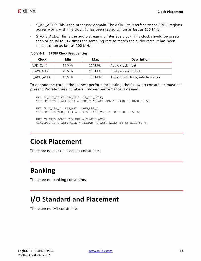
Clock FrequenciesThe core uses three clock domains. An asynchronous FIFO is used for cross clocking domain transfers.
• AUD_CLK_I: The SPDIF audio interface works with this clock. The frequency of the clock should be greater than or equal to 512 times the audio sampling rate for SPDIF in receive mode. It has been tested to run as fast as 100 MHz.
For SPDIF in transmit mode, the frequency of this clock should be a harmonic of the audio sampling rate and the corresponding divisor should be set in the SPDIF control register. For a 32 kHz sampling rate, 16.384 MHz is the minimum AUD_CLK_I rate required.
LogiCORE IP SPDIF v1.1 www.xilinx.com 33PG045 April 24, 2012
Clock Placement
• S_AXI_ACLK: This is the processor domain. The AXI4-Lite interface to the SPDIF register access works with this clock. It has been tested to run as fast as 135 MHz.
• S_AXIS_ACLK: This is the audio streaming interface clock. This clock should be greater than or equal to 512 times the sampling rate to match the audio rates. It has been tested to run as fast as 100 MHz.
To operate the core at the highest performance rating, the following constraints must be present. Prorate these numbers if slower performance is desired.
NET "S_AXI_ACLK" TNM_NET = S_AXI_ACLK;TIMESPEC TS_S_AXI_ACLK = PERIOD "S_AXI_ACLK" 7.408 ns HIGH 50 %;
NET "AUD_CLK_I" TNM_NET = AUD_CLK_I;TIMESPEC TS_AUD_CLK_I = PERIOD "AUD_CLK_I" 10 ns HIGH 50 %;
NET "S_AXIS_ACLK" TNM_NET = S_AXIS_ACLK;TIMESPEC TS_S_AXIS_ACLK = PERIOD "S_AXIS_ACLK" 10 ns HIGH 50 %;
Clock PlacementThere are no clock placement constraints.
BankingThere are no banking constraints.
I/O Standard and PlacementThere are no I/O constraints.
Table 4-1: SPDIF Clock Frequencies
Clock Min Max Description
AUD_CLK_I 16 MHz 100 MHz Audio clock input
S_AXI_ACLK 25 MHz 135 MHz Host processor clock
S_AXIS_ACLK 16 MHz 100 MHz Audio streamlining interface clock

LogiCORE IP SPDIF v1.1 www.xilinx.com 34PG045 April 24, 2012
Chapter 5
Designing with the CoreThis chapter includes additional information to make designing with the core easier.
SPDIF Register ModuleThis section describes the blocks within the SPDIF Register module.
AXI4-Lite IPIFThe SPDIF Register module provides the read/write control logic for the SPDIF core’s register set. The registers are accessible by the AXI4-Lite master interface through the AXI4-Lite IPIF module, which is part of the SPDIF Register module.
The data width of the AXI4-Lite interface is f ixed at 32 bits. The registers are defined in Table 2-6, page 16.
The interrupt control and soft reset functionality are also implemented as part of the SPDIF Register module. The SPDIF core can be reset by writing 0xA to the soft reset register. For an SPDIF transmitter, an SPDIF interrupt can be generated based on the FIFO Full/FIFO empty conditions. For an SPDIF receiver, in addition to the FIFO Full/FIFO Empty conditions, the interrupt is triggered if any preamble error/bi-phase mark code (BMC) error is detected over the SPDIF line or if the SPDIF core receives the start of block over the SPDIF line.
SPDIF DecoderThe enable bit in the Control register of the SPDIF Register module has to be set to enable the SPDIF decoder module. The SPDIF decoder recovers data from the bi-phase mark coded SPDIF data stream (see Bi-Phase Mark Code). The audio clock frequency should be at least eight times the bit rate 64 x FS. FS is the sampling frequency where each sample has 64 bits and in bi-phase mark code, each bit changes twice in a bit period). For example, to recover data from a 192 kHz sampling rate, the minimum audio clock frequency should be 8 x 64 x 192 kHz = 98.304 MHz to recover the data samples. As per SPDIF Protocol Preamble violates the bi-phase mark code format, SPDIF decoder module identif ies the channel number and the start of the audio block from the Preamble pattern.

LogiCORE IP SPDIF v1.1 www.xilinx.com 35PG045 April 24, 2012
SPDIF Register Module
The serial-to-parallel data conversion also takes place in the SPDIF Decoder module and then generates the FIFO write enables with the 32-bit FIFO input data. The sampling frequency information (that is, the count of audio clocks during the bit period) is updated in the Status Register of the SPDIF Register module.
This module detects the BMC/Preamble errors over the SPDIF line and reports to the SPDIF register module.
RX FIFO Control ModuleThe Asynchronous RX FIFO is used to store the 32-bit audio data received from the SPDIF decoder. The FIFO size is configurable and based on the C_AXIS_BUFFER_SIZE parameter generated. The data width of the FIFO is f ixed to 32 bits. This module receives the FIFO write input control and write data from the SPDIF decoder. When the FIFO reaches the full condition, an interrupt is generated and the RX FIFO Full status is updated through the status register of the SPDIF register module. Similarly, the RX FIFO empty interrupt and corresponding status are updated through the SPDIF interrupt status register.
AXI4-Stream Master InterfaceThe AXI4-Stream Master interface transfers the 32-bit parallel data read from the Non-Empty FIFO to the AXI4-Stream interface. The corresponding data valid signal (M_AXIS_TVALID) is set and the channel identif ier signal (M_AXIS_TID) is driven with the corresponding channel number. The channel number information is available to the AXI4-Stream Master interface through the SPDIF decoder. This module depends on the handshaking signal M_AXIS_TREADY issued from the AXI4-Stream interface target slave for completion of the transfer.
AXI4-Stream Slave InterfaceThe AXI4-Stream Slave interface receives the 32-bit streaming data from the target connected to the AXI4-Stream interface. This module generates the handshaking signal S_AXIS_TREADY after receiving the streaming data (S_AXIS_TDATA), data valid signal (S_AXIS_TVALID), and channel number identif ication (S_AXIS_TID). This also generates the TX FIFO write control signals and transfers the data received from the AXI4-Stream interface to TX FIFO Control Module. If the SPDIF TX FIFO is full, this module stops receiving the audio samples by driving the handshake signal S_AXIS_TREADY Low. This avoids the FIFO overrun condition in the SPDIF transmitter.
AXI4-Stream Data The data width over the AXI4-Stream interface is f ixed at 32 bits. Table 5-1 shows the 32-bit data format over the AXI4-Stream interface during audio data transmission and reception. All bit positions are as per the IEC60958-3 standard except for the preamble bit format.

LogiCORE IP SPDIF v1.1 www.xilinx.com 36PG045 April 24, 2012
SPDIF Register Module
The preamble provides the start of the audio block and audio channel information. The preamble patterns for the start of block, channel1 audio data, and channel2 audio data are listed in Table 5-2.
Bits [27:4] carry the audio data MSB bit at the 27th position and the LSB position is based on the audio sample length. Bit 28 provides the audio validity information. Bit 29 carries the user data information, and Bit 30 carries the channel status bit. Bit 31 is the even parity over 32 bits except for the preamble bits.
TX FIFO Control ModuleThe Asynchronous TX FIFO is used to store the 32-bit streaming data received from the AXI4-Stream slave interface. The FIFO size is configurable and based on the configuration parameter C_AXIS_BUFFER_SIZE generated. The data width of the FIFO is f ixed at 32 bits.
This module receives the FIFO write input control and write data from AXI4-Stream slave interface. When the FIFO reaches the full condition, an interrupt is generated and the TX FIFO Full status is updated through the interrupt status register of the SPDIF Register module. This condition can occur when the SPDIF enable bit is not set in the control register of the SPDIF Register module, and the target is sending continuous streaming data or when the value set for the C_AXIS_BUFFER_SIZE parameter is not sufficient.
The TX FIFO Control Module generates an TX FIFO_EMPTY interrupt when the TX FIFO becomes empty. This condition can occur if enough samples are not received by the SPDIF transmitter to send over the SPDIF line.
SPDIF EncoderThis module has to get the clock configuration bits through the control register to know the bit rate before SPDIF data transmission starts. The enable bit in Control register of the SPDIF Registers module has to be set to enable the SPDIF encoder module. The SPDIF encoder converts the 32-bit parallel data received from the TX FIFO to serial data. The serial data is transferred over the SPDIF interface in Bi-Phase Mark Code format with respect to the received bit rate information. The audio clock input has to be the harmonic of the sampling
Table 5-1: AXI4-Stream Audio Data Format
Bit 31 Bit 30 Bit 29 Bit 28 Bit[27:4] Bit[3:0]
Parity Channel Status Bit
User Data Bit
Validity Bit Audio Sample Data Preamble
Table 5-2: Preamble
Bit[3:0] Description
0001 Start of audio block
0010 Channel1 audio data
0011 Channel2 audio data

LogiCORE IP SPDIF v1.1 www.xilinx.com 37PG045 April 24, 2012
SPDIF Register Module
rate and should be higher than the bit rate. For example, for a 192 kHz sampling rate, 49.152 MHz or 98.3 MHz has to be provided as the core frequency (AUD_CLK_I) and the corresponding clock divisor information has to be given through the clock configuration register bits).
In case of a TX FIFO under-run condition, this module sends the null audio frames over the SPDIF line with the validity bit set. When the validity bit is set to 1, it means per the SPDIF protocol that the audio sample is invalid and the codec has to ignore the sample.
Note: The audio clock generation and the setting of clock configuration bits in the control register have to be done with care to support these sampling rates: 32 kHz, 44.1 kHz, 48 kHz, 88.2 kHz, 96 kHz, 176.4 kHz, and 192 kHz. The minimum audio clock frequency of 49.152 MHz or harmonic frequency of the same which is higher than this frequency supports the sampling rates of 32 kHz, 48 kHz, 96 kHz, and 192 kHz. The minimum audio clock frequency of 45.1584 MHz or harmonic frequency of the same which is higher than this frequency supports the sampling rates of 44.1 kHz, 88.2 kHz, and 176.4 kHz.
Bi-Phase Mark Code
The SPDIF interface (IEC-60958) is a consumer version of the AES/EBU-interface. The SPDIF digital signal is coded using the bi-phase mark code (BMC), which is a type of phase modulation. The bit clock, data bits, and BMC signals are shown in Figure 5-1.
The frequency of the clock is twice the bit rate. Every bit of the original data is represented as two logical states, which, together, form a cell. The length of a cell (time slot) is equal to the length of a data bit. The logical level at the start of a bit is always inverted to the level at the end of the previous bit. The level at the end of a bit is equal (a 0 is transmitted) or inverted (a 1 is transmitted) to the start of that bit. The BMC has either one or two transitions for every bit. Data bit 1 has two transitions during a bit period, and Data bit 0 has one transition during a bit period. As per protocol, except for the preambles, SPDIF audio data is transferred in the BMC format. Preambles violate the BMC to identify the channel information by the SPDIF receivers.
X-Ref Target - Figure 5-1
Figure 5-1: Bi-Phase Mark Code

LogiCORE IP SPDIF v1.1 www.xilinx.com 38PG045 April 24, 2012
Chapter 6
Detailed Example Design
Example DesignThis section provides instructions to generate an SPDIF core quickly, run the design through implementation with the Xilinx tools, and simulate the example design using the provided demonstration test bench.
OverviewFigure 6-1 and Figure 6-2 illustrate the SPDIF receiver and transmitter example designs, respectively. The example designs consist of the following:
• SPDIF netlist
• HDL wrapper which instantiates the SPDIF netlist
• Customizable demonstration test bench to simulate the example design
The SPDIF example designs have been tested with Xilinx® ISE® Design Suite v14.1 and the Mentor Graphics ModelSim simulator.
X-Ref Target - Figure 6-1
Figure 6-1: SPDIF Receiver Example Design

LogiCORE IP SPDIF v1.1 www.xilinx.com 39PG045 April 24, 2012
Example Design
Implementing an Example DesignAfter generating a core with either a Full-System Hardware Evaluation or Full license, the netlists and example design can be processed by the Xilinx implementation tools. The generated output files include scripts to assist you in running the Xilinx tools.
To implement an SPDIF example design, open a command prompt or terminal window and type these commands:
• For Windows:
ms-dos> cd <proj_dir>\quickstart\implementms-dos> implement.bat
• For Linux:
Linux-shell% cd <proj_dir>/quickstart/implementLinux-shell% ./implement.sh
These commands execute a script that synthesizes, builds, maps, and places-and-routes the example design. The script then generates a post-par simulation model for use in timing simulation. The resulting f iles are placed in the results directory.
Simulating an Example DesignThe SPDIF core provides a quick way to simulate and observe the behavior of the core by using the provided example designs. The simulation model provided is in Verilog.
X-Ref Target - Figure 6-2
Figure 6-2: SPDIF Transmitter Example Design

LogiCORE IP SPDIF v1.1 www.xilinx.com 40PG045 April 24, 2012
Demonstration Test Bench
Setting up for Simulation
The Xilinx UNISIM and SIMPRIM libraries must be mapped into the simulator. If the UNISIM or SIMPRIM libraries are not set for your environment, go to the Synthesis and Simulation Guide in the Xilinx Software Manuals for assistance compiling Xilinx simulation models. Simulation scripts are provided for ModelSim.
Functional SimulationThis section provides instructions for running a functional simulation of the SPDIF core using Verilog. Functional simulation models are provided when the core is generated. Implementing the core before simulating the functional models is not required.
To run a Verilog functional simulation of the example designs:
1. Set the current directory to:
<quickstart>/simulation/functional/
2. Launch the simulation script.
ModelSim: vsim -do simulate_mti.do
The simulation script compiles the functional simulation models and demonstration test bench, adds relevant signals to the wave window, and runs the simulation. To observe the operation of the core, inspect the simulation transcript and the waveform.
Demonstration Test Bench
Test Bench FunctionalityThe demonstration test bench is a Verilog f ile that exercises the example designs and the core itself. The test bench is provided as-is. Feedback is welcome but enhancements are not guaranteed.
The test bench consists of the following:
• AXI4-Lite master model to configure the core registers
• SPDIF RX driver model to drive the core input SPDIF line
• AXI4-Stream slave model to receive the data driven on AXI4-Stream master interface of the SPDIF core
• AXI4-Stream master model to drive the data on the AXI4-Stream slave interface of the SPDIF core

LogiCORE IP SPDIF v1.1 www.xilinx.com 41PG045 April 24, 2012
Demonstration Test Bench
• AXI4-Stream checker model to verify the data on the AXI4-Stream master interface of the SPDIF core
• SPDIF line checker model to verify the data on the SPDIF output line
• Test bench top file that instantiates all verif ication models and generates the necessary clocks required by the test bench
SPDIF Core in RX Mode Figure 3-1, page 31 shows the demonstration test bench in RX mode.
• Clock Generator
The sampling frequency at which the audio data is received on the core’s SPDIF input line is f ixed at 32 kHz. AUD_CLK_I, with 16.384 MHz frequency, is generated by the top-level module as required for the 32 kHz sampling frequency. The clock generator generates a reference clock for use by the test bench components.
• AXI4-Lite Master Model
In the AXI4-Lite Master Model, the SPDIF control register is set to 32'h00000001 to enable the SPDIF core.
• SPDIF RX Mode Driver
A sub-frame is a 32-bit audio sample with a 4-bit preamble and 28-bit audio data. A frame is a combination of 2 sub-frames (channel 0 and channel 1). The SPDIF RX Mode Driver model generates 1000 sub-frames to drive on the core’s SPDIF input line. This model also generates the preambles as required by the SPDIF protocol.
The 28-bit audio data generated by this model is an incremental pattern. This data is driven in bi-phase encoded format as specif ied by the SPDIF protocol.
The channel number is driven such that alternate channel IDs exist (channel 0 and channel 1).
• AXI4-Stream Slave Model
This model follows the AXI4-Stream protocol to receive the 32-bit streaming data driven on the AXI4-Stream master interface of the SPDIF core.
• AXI4-Stream RX Mode Checker
This model generates the expected incremental data and checks the data integrity of audio data received on the AXI4-Stream master interface of the SPDIF core. This model also checks the number of sub-frames (TIDs) received on the AXI4-Stream master interface of the SPDIF core.

LogiCORE IP SPDIF v1.1 www.xilinx.com 42PG045 April 24, 2012
Demonstration Test Bench
This model displays the completion of 50 sub-frames received on the AXI4-Stream master interface.
SPDIF Core in TX ModeThis section describes the functionality of the blocks in the demonstration test bench in TX mode.
• Clock Generator
The sampling frequency at which the audio data is transmitted on the core’s SPDIF output line is f ixed at 32 kHz. AUD_CLK_I is generated by the top-level module as required for the 32 kHz sampling frequency. AUD_CLK_I is generated for 49.152 MHz.
• AXI4-Lite Master Model
In the AXI4-Lite Master Model, the SPDIF control register is set to 32'h0000000D to enable the SPDIF core. This configuration sets the TX clock configuration bits to a value of 4'h3 (divisor 24).
• AXI4-Stream TX Mode Driver
The AXI4-Stream TX Mode Driver generates 1536 sub-frames of 32 bits to drive on the AXI4-Stream slave interface of the SPDIF core as defined in the AXI4-Stream protocol. This model generates the 4-bit preambles as required by the SPDIF protocol. The 28-bit audio data generated by this model is an incremental pattern.
The channel number is driven such that alternate channel IDs exist (channel 0 and channel 1).
• SPDIF TX Mode Checker
This model receives the data driven on the SPDIF output line. Every 64 bits of data are concatenated on the line, because the audio data is bi-phase encoded on the SPDIF output line. This model decodes the 56-bit data and generates the 28-bit audio data.
The channel ID is determined based on the received preamble on the SPDIF output line.
This model generates the expected 32-bit incremental data and compares with the data received on SPDIF output line.
This model displays the completion of 50 sub-frames received.

LogiCORE IP SPDIF v1.1 www.xilinx.com 43PG045 April 24, 2012
Appendix A
DebuggingSee Solution Centers in Appendix B for information helpful to the debugging progress.

LogiCORE IP SPDIF v1.1 www.xilinx.com 44PG045 April 24, 2012
Appendix B
Additional Resources
Xilinx ResourcesFor support resources such as Answers, Documentation, Downloads, and Forums, see the Xilinx Support website at:
www.xilinx.com/support.
For a glossary of technical terms used in Xilinx documentation, see:
www.xilinx.com/company/terms.htm.
Solution CentersSee the Xilinx Solution Centers for support on devices, software tools, and intellectual property at all stages of the design cycle. Topics include design assistance, advisories, and troubleshooting tips.
ReferencesThese documents provide supplemental material useful with this product guide:
1. AXI4 AMBA AXI Protocol Version: 2.0 Specification
2. IEC-60958-3 Standard Specification
3. AMBA AXI4-Stream Protocol Specification
4. DS160, Spartan-6 Family Overview
5. DS150, Virtex-6 Family Overview
6. DS768, LogiCORE IP AXI Interconnect Data Sheet
7. DS516, LogiCORE IP Interrupt Control Data Sheet

LogiCORE IP SPDIF v1.1 www.xilinx.com 45PG045 April 24, 2012
Technical Support
8. DS765, LogiCORE IP AXI Lite IPIF Data Sheet
9. UG767, LogiCORE IP DisplayPort User Guide
10. UG761, AXI Reference Guide
Technical SupportXilinx provides technical support at www.xilinx.com/support for this LogiCORE™ IP product when used as described in the product documentation. Xilinx cannot guarantee timing, functionality, or support of product if implemented in devices that are not defined in the documentation, if customized beyond that allowed in the product documentation, or if changes are made to any section of the design labeled DO NOT MODIFY.
See the IP Release Notes Guide (XTP025) for more information on this core. For each core, there is a master Answer Record that contains the Release Notes and Known Issues list for the core being used. The following information is listed for each version of the core:
• New Features
• Resolved Issues
• Known Issues
Ordering InformationThe core is provided under the Xilinx Core License Agreement and can be generated using the Xilinx® CORE Generator™ system. The CORE Generator system is shipped with the Xilinx ISE® Design Suite.
A simulation evaluation license for the core is shipped with the CORE Generator system. To access the full functionality of the core, including FPGA bitstream generation, a full license must be obtained from Xilinx. For more information, visit the DisplayPort product page.
Contact your local Xilinx sales representative for pricing and availability of additional Xilinx LogiCORE IP modules and software. Information about additional Xilinx LogiCORE IP modules is available on the Xilinx IP Center.

LogiCORE IP SPDIF v1.1 www.xilinx.com 46PG045 April 24, 2012
Revision History
Revision HistoryThe following table shows the revision history for this document.
Notice of DisclaimerThe information disclosed to you hereunder (the “Materials”) is provided solely for the selection and use of Xilinx products. To the maximum extent permitted by applicable law: (1) Materials are made available “AS IS” and with all faults, Xilinx hereby DISCLAIMS ALL WARRANTIES AND CONDITIONS, EXPRESS, IMPLIED, OR STATUTORY, INCLUDING BUT NOT LIMITED TO WARRANTIES OF MERCHANTABILITY, NON-INFRINGEMENT, OR FITNESS FOR ANY PARTICULAR PURPOSE; and (2) Xilinx shall not be liable (whether in contract or tort, including negligence, or under any other theory of liability) for any loss or damage of any kind or nature related to, arising under, or in connection with, the Materials (including your use of the Materials), including for any direct, indirect, special, incidental, or consequential loss or damage (including loss of data, profits, goodwill, or any type of loss or damage suffered as a result of any action brought by a third party) even if such damage or loss was reasonably foreseeable or Xilinx had been advised of the possibility of the same. Xilinx assumes no obligation to correct any errors contained in the Materials or to notify you of updates to the Materials or to product specifications. You may not reproduce, modify, distribute, or publicly display the Materials without prior written consent. Certain products are subject to the terms and conditions of the Limited Warranties which can be viewed at http://www.xilinx.com/warranty.htm; IP cores may be subject to warranty and support terms contained in a license issued to you by Xilinx. Xilinx products are not designed or intended to be fail-safe or for use in any application requiring fail-safe performance; you assume sole risk and liability for use of Xilinx products in Critical Applications: http://www.xilinx.com/warranty.htm#critapps.© Copyright 2012 Xilinx, Inc. Xilinx, the Xilinx logo, Artix, ISE, Kintex, Spartan, Virtex, Zynq, and other designated brands included herein are trademarks of Xilinx in the United States and other countries. AMBA, AMBA Designer, ARM, ARM1176JZ-S, CoreSight, Cortex, and PrimeCell are trademarks of ARM in the EU and other countries. All other trademarks are the property of their respective owners.
Date Version Revision
04/24/12 1.0 Initial Xilinx release.