1JTANDEMCOMPUTERS
ECL VLSI ASIClOOK Circuit DesignOptimization
Aurangzeb KhanDucLeDong NguyenBipolar VLSI Design GroupTandem VLSI
Technical Report 88.7August 1988Part Number 16257


ECL VLSI ASIC
lOOK CIRCUIT DESIGN
OPTIMIZATION
Aurangzeb Khan Duc Le Dong Nguyen
Bipolar VLSI Design Group, Tandem VLSI
Technical Report 88.7August 1988Part Number: 16257
Tandem Computers 8/9/88 1


ECL VLSI ASIC lOOK' CIRCUITDESIGN OPTIMIZATION
Aurangzeb Khan Due Le Dong Nguyen
June 1988
This paper illustrates the complex, inter-related design optimization choices required to achieveefficient, high speed silicon bipolar ECL VLSI ASICs. We present three possible design choicesfor ECL internal circuit design, and briefly discuss the trade-offs involved in our final choice. Wethen show the impact of this optimization on output driver circuit design, and for example, the needfor a new analytical framework to understand the lOOK performance of the chosen output circuitdesign. An analytical framework for the lOOK temperature compensation of an effective threelevel series-gated ECL output driver is then presented. This analysis was developed during thedesign of the output cell of a bipolar VLSI gate array IC. Results from this analysis have beenshown to agree quite well with actual measurements and computer-aided simulations.
Table of Contents
Overview
Internal Comparator DesignOutput Driver DesignCircuit Design Choices - Overview
Input Receiver Circuit Design
Input Receiver Circuit
Internal Comparator Circuit Design
Optimal ECL Internal Logic SwingStandard VBB-based Internal ComparatorCommon Mode VBB-based Internal ComparatorVrl-based Internal Comparator
lOOK Output Driver Design - Diode Stacking Considerations
Circuit Design Optimization - Conclusions
lOOK Output Temperature Compensation
ECL lOOK VOH and dVOH/dT Equations
ECL lOOK VOL and dVOL/dT Equations
RC/RCM Optimization
Conclusions
3
334
4
5
5
5678
9
13
13
14
15
16
18
Tandem Computers 8/9/88 2


OVERVIEW
Silicon bipolar ECL circuits attain fast switching speeds partially due to their small, well-controlledlogic voltage swing. Since the delay perfonnance of a digital circuit is proportional to its' logicswing, we note that excessive logic swing creates a delay penalty. However, if the logic voltageswing is too small compared to the total potential noise losses, we can attain marginal noisemargins, and consequently suffer from poor signal integrity. Thus a well-balanced logic voltageswing is optimized to provide reliable high speed operation with assured signal integrity.
Internal Comparator Design: System level electrical signals usually contain transient noisedue to a variety of sources such as, impedance variation, reflection, crosstalk, etc. This designexample illustrates how internal circuit design can have a major impact on output driver design.Let us define input receiver and internal comparator circuit functions. An IC input receiver circuitreceives off-chip signal inputs and provides buffered output signals with well-defined voltagelevels. It also provides good driving capability for driving other circuits within the IC. This circuituses the standard ECL first level comparator reference voltage, called VBB, to arbitrate high andlow level signals from inputs. Since the incoming system level signals are coded around thisreference voltage, our design choices are restricted to utilizing to VBB reference only. On theother hand, internal comparator circuits are used to perfonn a variety of logic functions within theIC. Such circuits receive signals from, and source signals to, other logic circuits within the IC.Since we have control of both the source and destination circuits, we can design any appropriatelogic swing, high and low levels, and comparator reference voltages. There are three options forinternal comparator circuit design:
1. Use standard VBB as Vr1. (Fig 1)
2. Use standard VBB and a common mode resistor offset. (Fig 2)
3. Use non-standard Vrl optimized to provide comparable VN1vIH, VNML. (Fig 3)
The first choice ensures signal compatibility with off-chip inputs. This enables a gate arrayarchitecture design which can accept off-chip inputs to any arbitrary location within the Ie, thusproviding usage flexibility, and reduced output driver cells' utilization. However, this techniquemakes the total logic swing too large, thus incurring a delay penalty.
The second choice also ensures signal compatibililty with off-chip inputs, thus providing usageflexibility, etc., as discussed above. Since the common mode offset resistor is used to tune thetotal logic swing to an optimal level, this technique does not incur a delay penalty. However, theneed for an extra component raises the silicon real estate cost of this solution, and also adds torouting complexity.
In the third design choice, we develop and use a non-standard ECL reference voltage, called Vrl,to optimize the total voltage swing without requiring a common mode offset resistor. This .:hoicehas the added benefit of facilitating three-level lOOK series-gating, thus providing enhanced circuitfunctionality at no incremental power. However, this choice restricts the ability of the arrayarchitecture to allow off-chip signal inputs to any location inside the IC, unless suitable CADprograms are developed to provide appropriate reference voltages which depend upon the source ofinput signals. Further, this technique requires two separate voltage regulators, versus one in theftrst two cases.
However, this approach ensures an optimal logic swing, eliminates the need for repetitive commonmode resistors, and provides an improved ECL three-level series-gating perfonnance. Our choicein this regard was further strengthened by our ability to get CAD software support which madeappropriate reference selection an automated function. Consequently, we reduced the total logic
Tandem Computers 8/9188 3

swing by 30%. This reduction is achieved without any loss in noise margin. It leads to a fasterpropagation time for no incremental power.
Output Driver Design: Having selected the non-standard Vrl-based circuit as our internal ECLdesign, we find that this significantly channels our output driver design choices, especially for aseries-gated lOOK ECL output driver.
In the lOOK output driver (Fig 3), Vrl cannot be applied directly to the output current switch firstlevel reference transistor, since this introduces a base/collector saturation hazard for the inputtransistor. Thus Vr2, which is the internal second level reference, is applied as the first levelreference voltage.
Vr2 =Vr1 - Vbe(Q9)
Therefore Vr3 becomes the second-level reference. However, note that Vr3 is offset from Vrl by2 Vbe, and thus represents a true third-level series-gating reference.
Vr3 =Vr2 - Vbe(Q13)
In a conventional ECL output driver design, Vr3 is not a viable voltage reference because threelevel deep series gating is not allowable. This follows from diode stacking considerations, asdescribed later. We are able to overcome this constraint only because we developed a currentmirror based comparator current mechanism. This allows an acceptable diode stacking, since acurrent mirror reduces ECL VEE min. requirements by -600 mV under nominal condition.
Diode stacking refers to a minimum ECL VEE requirement which depends on the number of seriesgating stages utilized in comparator design. In ECL, all reference voltage - Vrl, Vr2, Vr3, etc. are developed with respect to ECL VCC. Further, all current source voltages are developed withrespect to ECL VEE. The current source transistor is set-up so that its' base follows ECL VEE,while its' collector follows ECL VCe. If ECL VCC - ECL VEE falls below a critical minimum,defined as the diode stack, the current source can saturate. Such saturation causes unacceptablecircuit behaviour. Fig. 4 represents the conventional lOOK current source based approach. In thiscase,
ECL VEE min. = -4.48 V - 0.12 V = -4.60 V
Where 4.48V is the ECL VEE applied to the IC and 0.l2V is the Ohmic voltage loss in the Iepackage.
Fig. 3 represents our lOOK current mirror based approach. In this case,
ECL VEE min. =-3.92 V - 0.12 V = -4.04 V
which is well below the ECL VEE min. requirement for commercial range lOOK ECL VLSI ICs,and therefore represents an acceptable design.
Circuit Design Choices· Overview: In this section, the basic theme of this paper - designoptimization inter-relationships - has been presented in overview form. The following sectionsdiscuss the design trade-offs in more detail.
INPUT RECEIVER CIRCUIT DESIGN
ECL signals transmitted across digital systems' interconnect media follow well-defmed, standardECL VOH and VOL levels. On the driving side, ECL output drivers deliver digital informationencoded within specific high and low level voltage ranges. Usually however, such signals alsopick up unwanted transient noise spikes due to PCB impedance variation, reflection, crosstalk, etc.
Tandem Computers 8/9/88 4

On the receiving side, ECL receiverlbuffer circuits decode incoming system voltages and providebuffered driving capability within an IC. The receiverlbuffer comparator circuits arbitrate high andlow level inputs with respect to a reference voltage centred around the nominal ECL logic voltageswing. This voltage level, commonly called VBB, ensures adequate high and low level noisemargins, when nominal VIR, Vn... levels are input to the IC.
Input Receiver Circuit: A conventional ECL input receiver is presented in Fig. 1. This ECLswitch performs a buffer/driver function. It receives off-chip signal inputs at A and provides abuffered output at YA, such that YA = A. Standard ECL levels are input to this circuit. For lOOK,these levels are:
-880 mV > VIH> -1025 mV-1625 mV > VIL > -1810 mV
In order to ensure adequate noise margin levels when standard ECL I/O input levels are applied tothis input buffer, the reference voltage, Vrl = VBB, is chosen. At room temperature, nominalVBB is set to --1305mV. In this case, minimum noise margins can be defined as:
VNMHmin. =VIHmin. - VBBnom. = (-1025) - (-1305) =280 mVVNMLmin. = VBBnom. - VILmax. =(-1305) - (-1625) =320 mV
INTERNAL COMPARATOR CIRCUIT DESIGN
Using VBB as the reference voltage for the internal comparator creates a sub-optimal design.Essentially, this follows because internal data transmission voltages can be better controlled thanexternal, PCB level data transmission voltages. Thus, VOH, VOL levels within an IC can bedesigned to a smaller voltage swing. Optimal internal circuit design techniques also lead to internalVOH levels that differ from external VOH levels, making the use of the external VBB referencesub-optimal. In this section, we explore several design approaches to internal circuit optimization,and the impact these choices have on output driver design.
Optimal ECL Internal Logic Swing: The logic swing chosen for IC-internal logic circuitsmust ensure signal intergrity with fast operation. We can view the logic swing, VI, as made up oftwo components,
VI = VNMLoss + Vlmin.
In this equation, VNMLoss represents the potential worst-case noise margin losses and Vlminrepresents the minimum voltage difference required to ensure proper comparator operation. Vlmincan be understood as follows. If we assume matched devices, then comparator behaviourdepends on the voltage difference between the input applied to one comparator transistor's base,and the reference voltage applied to the other transistor's base. So,
Delta V = Yin - V,1 = VT*ln(IClIIC2)
This equation illustrates a fundamental aspect of the comparator function. For example, as theinput voltage rises 60 mV above the reference voltage, the current, ICS, is split in a 10: I ratiobetween ICI and IC2. The following table illustrates this aspect more comprehensively. Thenominal forward conduction voltage of the ECL switch transistors, Vbe, varies inversely withtemperature, which requires higher delta voltages at higher junction temperature.
Tandem Computers 8/9188 5

lcl:lc2Ratio
Delta V =f[Tj] (mV)-550C 270C 1250C
10:1100:1
1000:1
4590135
60120180
90180270
If we accpet Vlmin. as 180 mY, then we can expect a 1% error in internal VOL at a junctiontemperature of 125 degrees C. This is an acceptable design target. The other factor, VNMLoss,is used to account for noise margin loss mechanisms present within a large ASIC device. Suchmechanisms include Ohmic voltage losses on long routed signal nets, delta Vbe effects dut to ICS,IOEF programming, Wire-OR voltage losses, Vref variations, etc. Let us approximate the totalimpact of these factors to be 120 mV worst case, which is a reasonable target. Then we can dermethe optimal logic swing for our VLSI ASIC design to be,
VI =Optimal Logic Swing =600 mY.
Standard VBB-based internal comparator: Inside a VLSI IC, ECL VOH and VOL levelsdiffer from external input levels. With reference to Fig. 1, note that when input A is at a high levelwith respect to Vrl, the OR output YA attains,
and,VOH =ECL VCC - Vbe(Q4)
VNMH =VOH - Vr1
Conversely, when input A is at a low level with respect to VBB, the OR output YA attains,
where,
and,
VOL = ECL VCC - VI- Vbe(Q4)
VI =lCS*Rc
VNML =Vr1 - VOL
Usually, VNML = 300 mV is considered adequate. If the same reference voltage, VBB, is usedinside the IC, the internal high and low level noise margins can be defined as:
VNMHnom. =VOHnom. - VBBnom. = -760 mV + 1305 mV =545 mV
VNMLnom. =VBBnom. - VOLnom. =- 1305 mV + [845 mV + 760 mV] =300 mV
While such a design methodology ensures adequate VNMH and VNML values, it creates anexcessively large total logic voltage swing, VI. This follows because,
VI =VOH - VOL =VNMH + VNML =845 mV
and VNMH is over-designed at 545 mY. Since the delay performance of this circuit isproportional to its logic swing, this excessive logic swing creates a delay penalty.
Tandem Computers 8/9/88 6

ECL VCC
VBBA
RC
YA
VCS
ECL VEE
Fig. 1: Conventional ECL Switch
Common-mode VBB-based internal comparator: One design technique used to balancethe VNMH and VNML values, and thus optimize the total logic swing, is to use a common modeoffset resistor. Such an ECL current switch is shown in Fig. 2. In this case,
where,
where,
VI =VOH - VOL
VOH = vee - Vem - Vbe(Q4)VOL = vee - (Vem + Vdm) - Vbe(Q4)
Vem =Ies * RemVdm =Ies * Rdm
and, by design,
VI =Vdm
This circuit reduces the excessive VNMH by developing a common mode offset voltage, Vern,across Rem. While this technique successfully addressses the excessive swing issue, it creates theneed for an additional component in each ECL current switch. In a large VLSI IC, such additionalcomponents can consume considerable Silicon real estate.
Tandem Computers 8/9/88 7

ECL VCC
RDM
A
ECL VEE
VBB
YA
VCS
Fig. 2: EeL Switch with Voh Offset Resistance
Vrl-based internal comparator: A third design technique used to balance the VNMH andVNML values, and thus optimize the total logic swing, is to use a non-standard ECL referencevoltage. Such an ECL current switch is identical to the conventional circuit presented in Fig. 1,except that the reference voltage, Vrl, is chosen to balance both VNMH and VNML with anoptimally minimized total logic swing. In this case, with reference to Fig. 1, when input A is at ahigh level with respect to Vrl, the OR output YA attains,
so,VOH = ECL VCC - Vbe(Q4)
VNMH =VOH - Vr]
Conversely, when input A is at a low level with respect to Vrl, the OR output YA attains,
where,
and,
VOL =ECL VCC - VI- Vbe(Q4)
VI =ICS*Rc
VNML =Vr] - VOL
Usually, VNML = 300 mV is considered adequate at room temperature. The optimal referencevoltage, Vr!, to be used inside the IC, can be developed as follows:
Tandem Computers 8/9/88 8

Vr1nom. =VOHnom. - VNMHnom.= -760 mV - 300 mV=-1060 mV
Then,VNMHnom. =VOHnom. - Vr1nom. =-760 mV + 1060 mV =300 mV
and,VNMLnom. =Vr1nom. - VOLnom. =-1060 mV + 600 mV + 760 mV =300 mV
where,VI =ICS*Rc =600 mV
This design methodology ensures adequate VNMH and VNML values and creates an optimal totallogic voltage swing, VI, without requiring a common mode resistor. It reduces the excessiveVNMH of the conventional approach by developing a reference voltage optimized for internalvoltage swing values.
The benefits of this technique are a 30% reduction - from 845 mV to 600 mV - in the total logicswing, without any loss of high or low noise margin. Thus the delay performance of the circuit isimproved significantly without requiring any increase in power dissipation.
lOOK OUTPUT DRIVER DESIGN - DIODE STACKING CONSIDERATIONS
Our choice of the third design technique mentioned above places some new constraints on thedesign of a series-gated lOOK ECL output driver. Specifically, the internal reference voltage, Vrl,cannot be applied directly to the output current switch first level reference transistor, sincc~ thisintroduces a base/collector saturation hazard when the current ICM (Fig. 3) is switched to place theoutput at a low level. In order to eliminate this saturation hazard, Vr2 ( which is usually a secondlevel reference) is applied as the first level reference voltage.
Vr2 =Vr1 - Vbe(Q9)
Consequently, the internal input voltage levels, which are normally centred around Vrl, are emitterfollower shifted to switch properly against Vr2. The use of Vr2 as the primary reference requiresthe use of Vr3 as the second-level reference. In this case,
Vr3 =Vr2 - Vbe(Q13)
Note that Vr3 is offset from Vrl by 2 Vbe voltages, and thus represents a true third level seriesgating reference. This low voltage reference necessitates the use of a current mirror circuit in orderto ensure an acceptable diode stacking for lOOK operation.
Tandem Computers 8/9/88 9

RT
50 Ohms
VTT (= .2V)
VR3Qll
ICS lRIEF2RIEFI
ECL VCC ECL VCCA
RC !I2 U! RC llCHor
A ICL
Q9
Q6B
QIO
ECL VEE
Fig. 4: Conventional Two Level lOOK ECL Output Driver
The diode stacking can be illustrated with reference to Fig. 4, which represents the conventionallOOK current source based approach as in [1], [2], and [3]. In this circuit, note that Vr2 and Vr3follow ECL VCC, while VCS follows ECL VEE. So the lowest voltage on the collector of thecurrent source transistor, Q8, with respect to ECL VCC, is:
Vc(Q8) =ECL VCC -/VrJ/ - Vbe(Q12)
Now, the voltage at the base of this current source transistor, Q8, with respect to ECL VCC is:
Vb(Q8) =ECL VCC -/ECL VEE/ + VCS
Therefore,
Vbc(Q8) =[ECL VCC - IECL VEEI + VCS]- [ECL VCC - IVr3/- Vbe(Q12)]=ECL VCC -/ECL VEE/ + VCS - ECL VCC + /VrJ/ + Vbe(Q12)=-/ECL VEE/ + VCS + /Vr3/ + Vbe(Q12)
Tandem Computers 8/9/88 10
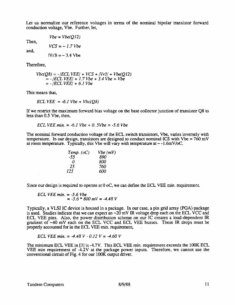
Let us nonnalize our reference voltages in tenns of the nominal bipolar transistor forwardconduction voltage, Vbe. Further, let,
Then,
and,
Therefore,
Vbe = Vbe(Q12)
VCS = -1.7 Vbe
IVr31 = - 3.4 Vbe
Vbc(Q8) =-JECL VEEj + VCS + jVr3j + Vbe(Q12)=-JECL VEEj + 1.7 Vbe + 3.4 Vbe + Vbe=-JECL VEEj + 6.1 Vbe
This means that,
ECL VEE = -6.1 Vbe + Vbc(Q8)
If we restrict the maximum forward bias voltage on the base collector junction of transistor Q8 toless than 0.5 Vbe, then,
ECL VEE min. =-6.1 Vbe + O. 5Vbe =-5.6 Vbe
The nominal forward conduction voltage of the ECL switch transistors, Vbe, varies inversely withtemperature. In our design, transistors are designed to conduct nominal ICS with Vbe =76Q mVat room temperature. Typically, this Vbe will vary with temperature at - -1.6mV10C.
Temp. (oC)-55o
25125
Vbe (mV)890800760600
Since our design is required to operate at 0 oC, we can defme the ECL VEE min. requirement.
ECL VEE min. = -5.6 Vbe=-5.6 * 800 mV =-4.48 V
Typically, a VLSI IC device is housed in a package. In our case, a pin grid array (PGA) packageis used. Studies indicate that we can expect an -20 mV IR voltage drop each on the ECL vec andECL VEE pins. Also, the power distribution scheme on our IC creates a load-dependent IRgradient of -40 mVeach on the ECL VCC and ECL VEE busses. These IR drops must beproperly accounted for in the ECL VEE min. requirement,
ECL VEE min. = -4.48 V - 0.12 V = -4.60 V
The minimum ECL VEE in [3] is -4.7V. This ECL VEE min. requirement exceeds the lOOK ECLVEE min requirement of -4.2V at the package power inputs. Therefore, we cannot use theconventional circuit of Fig. 4 for our lOOK output driver.
Tandem Computers 8/9/88 11

!ICHorICL
Q6
VTT (= -2V)
ECL VCCA
VX
(VCS + CI»
RT
50 OhmsVR3
RCM
Q7ICMI.Q8
Qll
RIEF2RIEFl
ECL VCC
RC !I2 n! RC
A
Q9
B
QlOQ2
ECL VEE
Fig. 3: Three Level Series Gated lOOK EeL Output Drivel'
We developed the schematic shown in Fig. 3 to improve the ECL VEE min. functionality of ourVLSI IC design. The use of a current mirror effectively reduces the ECL VEE min. require:mentsto acceptable levels. The diode stacking can be illustrated with reference to Fig. 3, whichrepresents our lOOK approach. In this circuit, the lowest voltage on the collector of the (:urrentsource transistor, Q8, with respect to ECL VCC, is:
Vc(Q8) =ECL VCC - /Vr3/ - Vbe(Q12)
Now, the voltage at the base of this current source transistor, Q8, with respect to ECL VCC is:
Vb(Q8) =ECL VCC - JECL VEEj + Vbe(Q8)
Therefore,
Vbc(Q8) = [ECL VCC - /ECL VEE/ + Vbe(Q8)] - [ECL VCC - /Vr3/ - Vbe(Q12)]= ECL VCC - /ECL VEE/ + Vbe(Q8) - ECL VCC + /Vr3/ + Vbe(Q12)=-/ECL VEE/ + Vbe(Q8) + /Vr3/ + Vbe(Q12)
Let us nonnalize our reference voltages in tenns of the nominal forward conduction voltage, Vbe.Further, let,
Tandem Computers 8/9/88 12

and,
Therefore,
Vbe = Vbe(Q12) = Vbe(Q8)
/VrJ/ =- 3.4 Vbe
Vbc(Q8) =-/ECL VEE/ + Vbe(Q8) + /VrJ/ + Vbe(Q12)=-/ECL VEE/ + Vbe + 3.4 Vbe + Vbe=-/ECL VEE/ + 5.4 Vbe
This means that.
ECL VEE =-5.4 Vbe + Vbc(Q8)
If we restrict the maximum forward bias voltage on the base collector junction of transistor Q8 toless than 0.5 Vbe. then.
ECL VEE min. = -5.4 Vbe + O. 5Vbe = -4.9 Vbe
Our design is required to operate at 0 oC. we can define the ECL VEE min. requirement.
ECL VEE min. =-4.9 Vbe=-4.9 * 800 mV =-3.92 V
Accounting for IR voltage drops,
ECL VEE min. =-3.92 V· 0.12 V =-4.04 V
This ECL VEE min. requirement is well within the lOOK ECL VEE min requirement of -4.2V atthe package power inputs.
CIRCUIT DESIGN OPTIMIZATION· CONCLUSIONS
We have shown the impact of internal ECL circuit optimization - with respect to logic swing andcomponent count· on ECL output circuit design. The additional design constraints added by lOOKoperation requirements are also addressed. We find that the resulting circuit requires a newframework for effective lOOK optimization of VOH, VOL temperature dependence. The followingsection develops this framework, and provides some guidelines for lOOK optimization.
lOOK OUTPUT TEMPERATURE COMPENSATION
Thus far, we have presented design trade-offs based on functionality and diode stackingconsiderations, which have led to the use of an effectively three-level series-gated ECL outputdriver. In order to accommodate three-level deep series-gating, this circuit employed a currentmirror technique to reduce maximum voltage diode stacking to within lOOK ECL VEE min. limits.
lOOK output levels, as distinct from lOKH output levels. exhibit near-perfect independence fromtemperature and power supply voltage variations. In particular, as the IC junction temperature isvaried from 0 degrees C to 125 degrees C, we find that the IC output lOOK levels remain withinthe temperature invariant bounds,
-880 mV <= VOH <= -1025 mY,-1625mV <= VOL <= -1810 mY.
Tandem Computers 819/88 13

Now we explore the design trade-offs required for successful lOOK operation of this circuit.VOH, VOL equations are first presented, followed by dVOH/dT and dVOljdT equations. Thedesign trade-offs inherent in these equations are then discussed, and some optimizationrecommendations made.
The VOH, VOL equations for the lOOK series-gated ECL output driver as shown in Fig. 3, are:
VOH= -{n * h**2 * RC(h+l)**2 RCM
VOL= -{2n * h**2 * RC(h+l)**2 RCM
In these equations,
(VCS-VBE) - 2RC*VIT - VDH + 3VBEH}/{3 + 2RC )(h+l)RT (h+l)RT
(VCS-VBE) - 2RC*VIT + VDL + 3VBEH}I{3 + 2RC )(h+1)RT (h+l)RT
n = Number of Emitters in the current mirror transistor. Defines Irefvs. ICM ratio.h =Transistor forward conduction current gain, commonly referred to as "Beta".
RC = Output comparator collector resistor (See Fig. 3).RCM = Current mirror resistor (See Fig. 3).VCS = Current Source voltage reference. VX-VBE = VCS. (See Fig. 3)VBE = Transistor forward conduction voltage, for Q7 (See Fig. 3).VTI = Output termination voltage, typically -2V.
RT = Output termination resistor, typically 50 Ohms.VOH = Transistor forward conduction voltage for Q5 (See Fig. 3).VOL = Transistor forward conduction voltage for Q4 (See Fig. 3).
VBEH = Transistor forward conduction voltage for Q6 (See Fig. 3).
Through these equations, we find that the temperature dependence of VOH and VOL can beadjusted by tuning the RC/RCM ratio. This is a unique aspect of this circuit. It effectivelyinvalidates the application of conventional lOOK output circuit temperature analysis to thisproblem. Therefore, we develop a new analysis which can be used to successfully design theappropriate lOOK temperature independence. In order to do this, we must first select the desiredVOH and VOL levels. Once these are known, we can solve for RC and RCM from the equationspresented above. Since RCM defines the output comparator current, ICM, it effectively controlsthe propagation delay of the output circuit also. Throught the use of computer-based circuitsimulators, such as SPICE, we can determine the appropriate ICM required to meet delayperformance objectives. This required ICM dictates the appropriate RCM value. The RC value isthen determined based on the required output logic swing. Since RC has a direct impact on theVOHmax. requirement, in practice IeM is over-designed to ensure an acceptably small value forRC. Typically, RC is less than 300 Ohms.
Once initial RC, RCM and n values have been determined, we can find anew, more optimized,RC/RCM ratio by solving the equations given below simultaneously. Note that the RC/RCM ratioaffects not only VOH and VOL, but also dVOH/dT and dVOljdT. Thus the new RC/RCM ratioderived above is not optimized for VOH, VOL temperature compensation. VOH, VOL, dVOH/dTand dVOL/dT need to be solved simultaneously in order to obtain minimal temperaturedependence. Therefore, we develop a unique technique to achieve desired VOH, VOL withminimal dVOH/DT and dVOljdT as follows.
ECL lOOK VOH & dVOH/dT EQUATIONS
Assume A and B are both at a logic H (high) in order to obtain a logic H at the output
VOH= -{n * h**2 * RC(h+1)**2 RCM
Tandem Computers
(VCS-VBE) - 2RC*VIT - VDH + 3VBEH}I{3 + 2RC )(h+l)RT (h+1)RT
(1)
8/9/88 14
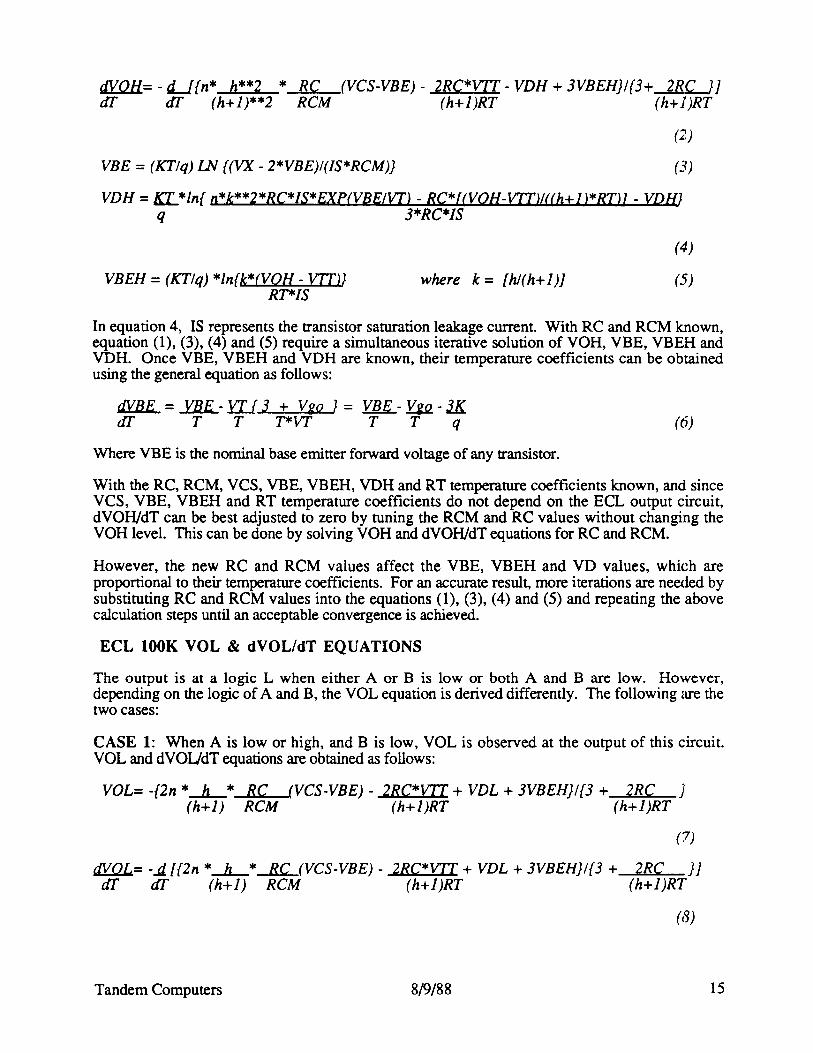
dVQH= - rLl{n* h**2 * Re (VeS-VBE) - 2Rc*m - VDH + 3VBEH}/{3+ 2Re )}dT dT (h+1)**2 ReM (h+l)RT (h+l')RT
(2)
VBE = (KTlq) IN {(VX - 2*VBE)I(IS*ReM)} (3)
VDH =KL*ln{ n*k**2*RC*IS*EXP(VBE/VT) - RC*UVOH-WU((h+J)*RTH - VDH}q 3*Re~S
VBEH =(KT/q) *In{k*(YOH - WURT*IS
where k = [h/(h+l)}
(4)
(5)
In equation 4, IS represents the transistor saturation leakage current. With RC and RCM known,equation (1), (3), (4) and (5) require a simultaneous iterative solution of VOH, VBE, VBEH andVDH. Once VBE, VBEH and VDH are known, their temperature coefficients can be obtainedusing the general equation as follows:
dYBE =.YllE-- YI.13 + V~Q ) = VBE -w-lKdT T T T*VT T T q
Where VBE is the nominal base emitter forward voltage of any transistor.
(6)
With the RC, RCM, VCS, VBE, VBEH, VDH and RT temperature coefficients known, and sinceVCS, VBE, VBEH and RT temperature coefficients do not depend on the ECL output circuit,dVOH/dT can be best adjusted to zero by tuning the RCM and RC values without changing theVOH level. This can be done by solving VOH and dVOH/dT equations for RC and RCM.
However, the new RC and RCM values affect the VBE, VBEH and VD values, whkh areproportional to their temperature coefficients. For an accurate result, more iterations are needed bysubstituting RC and RCM values into the equations (1), (3), (4) and (5) and repeating the abovecalculation steps until an acceptable convergence is achieved.
ECL lOOK VOL & dVOL/dT EQUATIONS
The output is at a logic L when either A or B is low or both A and B are low. However,depending on the logic of A and B, the VOL equation is derived differently. The following are thetwo cases:
CASE 1: When A is low or high, and B is low, VOL is observed at the output of this circuit.VOL and dVOljdT equations are obtained as follows:
VOL= -(2n *--h..-* Re(h+l) ReM
(VeS-VBE) - 2Re*m + VDL + 3VBEH}/{3 + 2RC )(h+l)RT (h+l)RT
(7)
dY..QL.= -.Ji.[(2n *--h..-* Re (VeS-VBE) - 2Re*w + VDL + 3VBEH}I{3 + 2Re )]dT dT (h+1) ReM (h+1)RT (h+l)RT
(8)
Tandem Computers 8/9/88 15

VOL= -{2n * h**2 * RC(h+1)**2 ReM
CASE 2: When B is high and A is low, VOL is observed at the output of this circuit. VOL anddVOUdT equations are obtained as follows:
(VCS-VBE) - 2RC*YIT + VDL + 3VBEH}/{3 + 2RC }(h+1)RT (h+1)RT
(9)
dY.QL.= -.d. [{2n * h**2 * Re (VeS-VBE) - 2Re*m + VDL + 3VBEH}/{3 + 2Re }]ar ar (h+1)**2 RCM (h+1)RT (h+1)RT
(10)
The only difference between Eq. (8) and Eq. (10) is the additional h/(h+1) factor in Eq. (10) whichis always smaller than one. Therefore, Eq. (8) is greater than Eq. (10). Since Eq. (8) is greaterthan the Eq.(lO), there is a very negligible error obtained if Eq.(10) is ignored. Therefore, we willuse Eq.(8) to obtain a desirable VOL level with minimal dVOUdT.
With equations (11), (12), (13), the RC and RCM values are solved using the same method asexplained in the VOH section.
VBE = (KT/q) * In {(VX - 2*VBE)/(IS*RCM)}
VDL = KI. * In ( n*k*RC*IS*EXP(YBE/VT) + RC*UVOL-WU((h+ll*RT)l - VDUq 3 * RC * IS
VBEL =(KT/q) * In (k*(VOL-W)/(RT*IS)}
RCIRCM OPTIMIZATION
(11)
(12)
(13)
To achieve dVOH/dT = 0 and dVOL/dT = 0, two different ratios of RC/RCM are required, as canbe seen from our analysis. This means that we cannot simultaneously get zero temperaturedependence for both VOH and VOL. Since we have to choose one ratio of RC/RCM to get thephysical RC and RCM values, an optimal way to determine this ratio is to equate dVOH/dT anddVOUdT,
dVOH/dT = dVOUdT,
and solve for RClRCM. By using this criterion, desirable VOH and VOL and minimal dVOH/dTand dVOUdT can be achieved.
In the following graph, titled VOH & VOL VS. RC/RCM, we present various RC/RCM ratios,and show their impact on VOH, VOL, dVOH/dT and dVOUdT. We find that the optimal valuesfor our application are,
RC = 269 OhmsRCM = 631 Ohms
RC/RCM =0.43.
Tandem Computers 8/9/88 16

VOH at VOL VS. RC/RCM
With these optimized values, the perfonnance of the output driver is,
Output Levels =f(Junction Temperature, degrees C) Comments
0 25 125
VOH(mV) = -979 -959 -892 PredictedVOH(mV) = -1000 -975 -910 SimulatedVOH(mV) = -995 -980 -920 Measured
VOL(mV) = -1778 -1752 -1681 PredictedVOL (mV) = -1775 -1750 -1645 SimulatedVOL(mV) = -1755 -1735 -1660 Measured
In the next graph, titled PREDICTION VS. SIMULATION VS. MEASUREMENT, we presentpredicted, simulated and measured perfonnance of our output circuit based on the values statedabove. In general, we find good agreement between prediction and measurement. Since oursimulations are for the nominal process, and do not acount for long metal interconnect between thebase of Q6 and Re, in Fig. 3, we find some deviation between measured and predictedperfonnance. This slight deviation also reflects upon the accuracy of computer models for ourdevices.
Tandem Computers 8/9/88 17

PREDICTION VS. SIMULATION VS. MEASUREMENT
We conclude that our analytical framework, as presented in this paper, has thus been verified byactual measurements.
CONCLUSIONS
In this paper, we have attempted to illustrate the complex, inter-related design optimization choicesrequired to achieve efficient, high speed silicon bipolar ECL VLSI ASICs. We presented threepossible design choices for an IC-internal comparator circuit, and then showed how our chosendesign methodology ensures adequate VNMH and VNML values and creates an optimal total logicvoltage swing, VI, without requiring a common mode resistor. It reduces the excessive VNMH ofthe conventional approach by developing a reference voltage optimized for internal voltage swingvalues. The benefits of this technique are a 30% reduction - from 845 mV to 600 mV - in the totallogic swing, without any loss of high or low noise margin. Thus the delay performance of thecircuit is improved significantly without requiring any increase in power dissipation.
We then showed the impact of this optimization on output driver circuit design, and for example,the need for a new analytical framework to understand the lOOK performance of the chosen outputcircuit design. An analytical framework for the WOK temperature compensation of an effectivethree-level series-gated ECL output driver was then developed and presented. To minimize overalltemperature dependence of VOH and VOL, we proposed,
dVOH/dT = dVOL/dT
as the optimization criterion. This is a requirement because, in order to achieve dVOH/dT = 0 anddVOl../dT = 0, two different ratios of RC/RCM are required. Since we have to choose one I1ltio of
Tandem Computers 8/9188 18

RC/RCM to get RC and RCM values, the best way to determine this ratio is to equate dVOH/dTand dVOLJdT (dVOH/dT =dVOLJdT) and solve for RC/RCM. By this method desirable VOHand VOL and minimal dVOH/dT and dVOLJdT can be achieved.
The actual circuit used in our ECL VLSI ASIC devices conformed to this criterion. Thes devicesare the basis of a high speed digital system currently under development. Results from thisanalysis have been shown to agree quite well with actual measurements made on such VLSIdevices, as well as computer-aided simulations.
REFERENCES
[1] P. R. Marley, "On-chip Temperature Compensation for ECL," Electron Products, Mar. 1,1971.
[2] P. R. Marley, "Design Considerations of Temperature Compensated Emitter Coupled Logic,"presented at the IEEE Int. Conv., Mar. 1971.
[3] H. H. Muller, W. K. Owens, and P. W. J. Verhofstadt, "Fully Compensated Emitter-CoupleLogic: Eliminating the Drawbacks of Conventional ECL," IEEE Journal of Solid-State Circu:lts,vol. SC-8, No.5, Oct. 1973.
AUTHORS
Aurangzeb Khan: A. Khan is Manager of Bipolar VLSI Development at Tandem Computers,Inc. He has been at Tandem since October, 1983, where he has been involved with chiparchitecture, circuit design and CAD methodology aspects of high performance bipolar ECL ASICdesign, as well as high speed system interconnect issues. In March 1988, he received TandemTOPS, and in May 1988, he received the Tandem TSD Award for Technical Excellence. He holdsseveral patents in high speed circuit desigin for ECL VLSI ICs.
In December 1975, Aurangzeb completed a B.Sc. at the University of The Punjab, in Pakistan, inPhysics/Mathematics, with highest academic honors. He then attended University of Califomia atBerkeley, completing a double major BSEECS, BSNE (Electrical Engineeering and NuclearEngineering) in December 1978. In January 1979, he joined Fairchild Semiconductor to designhigh speed ECL static RAMs. Concurrently, he attended Stanford University where, in March1981, he obtained an MSEE, and in June 1984, an MSEM. Aurangzeb played varsity andcompetitive Squash Racquets in Pakistan, at Berkeley and at Stanford. He is interested inphotography and travel.
Duc Le: Duc Le was born in Vietnam, on July 29, 1961. As a result of the war, he left his owncountry and arrived in the USA in June 1980. Mr. Le received the B.S. degree in ElectricalEngineering and Computer Science from University of California at Berkeley. In June 1988, hecompleted an MSEE degree at Stanford University in Electrical Engineering and ComputerScience. Mr. Le is a bipolar VLSI Development Engineer at Tandem Computers, Inc. inCupertino, California. His work includes analysis and design of Bipolar ECL gate arrays. Healso contributes to CAD tool development. Mr. Le is a member of the IEEE.
Dong Nguyen: D. V. Nguyen graduated with a B.S. degree in Electrical Engineering andComputer Science from University of California at Berkeley in 1986. Currently, he is pursuing aM.S. degree in EECS at University of Santa Clara. In 1986 he joined Tandem Computer Inc.,where he has been involved in high-speed ECL circuit design and development. His main areas ofinterest are high-speed circuit design and VLSI technology. Mr. Nguyen is a member of the IEEEand Tau Beta Pi.
Tandem Computers 8/9/88 19


Distributed by'1TANDEMCOMPUTERS
Corporate Information Center19333 Valko Parkway MS3-07Cupertino, CA 95014-2599

Recommended