Embed Size (px)
Citation preview

Vivado Design Suite Properties Reference Guide
UG912 (v2013.1) March 20, 2013

Properties Reference Guide www.xilinx.com 2UG912 (v2013.1) March 20, 2013
Notice of DisclaimerThe information disclosed to you hereunder (the “Materials”) is provided solely for the selection and use of Xilinx products. To the maximum extent permitted by applicable law: (1) Materials are made available "AS IS" and with all faults, Xilinx hereby DISCLAIMS ALL WARRANTIES AND CONDITIONS, EXPRESS, IMPLIED, OR STATUTORY, INCLUDING BUT NOT LIMITED TO WARRANTIES OF MERCHANTABILITY, NON-INFRINGEMENT, OR FITNESS FOR ANY PARTICULAR PURPOSE; and (2) Xilinx shall not be liable (whether in contract or tort, including negligence, or under any other theory of liability) for any loss or damage of any kind or nature related to, arising under, or in connection with, the Materials (including your use of the Materials), including for any direct, indirect, special, incidental, or consequential loss or damage (including loss of data, profits, goodwill, or any type of loss or damage suffered as a result of any action brought by a third party) even if such damage or loss was reasonably foreseeable or Xilinx had been advised of the possibility of the same. Xilinx assumes no obligation to correct any errors contained in the Materials or to notify you of updates to the Materials or to product specifications. You may not reproduce, modify, distribute, or publicly display the Materials without prior written consent. Certain products are subject to the terms and conditions of the Limited Warranties which can be viewed at http://www.xilinx.com/warranty.htm; IP cores may be subject to warranty and support terms contained in a license issued to you by Xilinx. Xilinx products are not designed or intended to be fail-safe or for use in any application requiring fail-safe performance; you assume sole risk and liability for use of Xilinx products in Critical Applications: http://www.xilinx.com/warranty.htm#critapps.© Copyright 2012-2013 Xilinx, Inc. Xilinx, the Xilinx logo, Artix, ISE, Kintex, Spartan, Virtex, Vivado, Zynq, and other designated brands included herein are trademarks of Xilinx in the United States and other countries. All other trademarks are the property of their respective owners.
Revision HistoryThe following table shows the revision history for this document.
Date Version Revision
03/20/2013 2013.1 Edited details of DCI_CASCADE, DIFF_TERM, and IOB. Added IOBDELAY, KEEPER, OUT_TERM, PULLUP, PULLDOWN, POST_CRC, POST_CRC_ACTION, POST_CRC_FREQ, POST_CRC_INIT_FLAG, and POST_CRC_SOURCE, properties.

Properties Reference Guide www.xilinx.com 3UG912 (v2013.1) March 20, 2013
Table of ContentsChapter 1: Introduction
Copying Examples from this Document . . . . . . . . . . . . . . . . . . . . . . . . . . . . . . . . . . . . . . . . . . . . . . . . 5About This Guide . . . . . . . . . . . . . . . . . . . . . . . . . . . . . . . . . . . . . . . . . . . . . . . . . . . . . . . . . . . . . . . . . . 5
Chapter 2: Vivado Design Suite PropertiesProperties Information . . . . . . . . . . . . . . . . . . . . . . . . . . . . . . . . . . . . . . . . . . . . . . . . . . . . . . . . . . . . . 7ASYNC_REG . . . . . . . . . . . . . . . . . . . . . . . . . . . . . . . . . . . . . . . . . . . . . . . . . . . . . . . . . . . . . . . . . . . . . . 8BEL. . . . . . . . . . . . . . . . . . . . . . . . . . . . . . . . . . . . . . . . . . . . . . . . . . . . . . . . . . . . . . . . . . . . . . . . . . . . . 12CLOCK_DEDICATED_ROUTE. . . . . . . . . . . . . . . . . . . . . . . . . . . . . . . . . . . . . . . . . . . . . . . . . . . . . . . . . 15COMPATIBLE_CONFIG_MODES. . . . . . . . . . . . . . . . . . . . . . . . . . . . . . . . . . . . . . . . . . . . . . . . . . . . . . 17DCI_CASCADE . . . . . . . . . . . . . . . . . . . . . . . . . . . . . . . . . . . . . . . . . . . . . . . . . . . . . . . . . . . . . . . . . . . . 19DIFF_TERM . . . . . . . . . . . . . . . . . . . . . . . . . . . . . . . . . . . . . . . . . . . . . . . . . . . . . . . . . . . . . . . . . . . . . . 21DONT_TOUCH. . . . . . . . . . . . . . . . . . . . . . . . . . . . . . . . . . . . . . . . . . . . . . . . . . . . . . . . . . . . . . . . . . . . 24DRIVE . . . . . . . . . . . . . . . . . . . . . . . . . . . . . . . . . . . . . . . . . . . . . . . . . . . . . . . . . . . . . . . . . . . . . . . . . . 26HIODELAY_GROUP . . . . . . . . . . . . . . . . . . . . . . . . . . . . . . . . . . . . . . . . . . . . . . . . . . . . . . . . . . . . . . . . 29HLUTNM . . . . . . . . . . . . . . . . . . . . . . . . . . . . . . . . . . . . . . . . . . . . . . . . . . . . . . . . . . . . . . . . . . . . . . . . 32IN_TERM . . . . . . . . . . . . . . . . . . . . . . . . . . . . . . . . . . . . . . . . . . . . . . . . . . . . . . . . . . . . . . . . . . . . . . . . 36INTERNAL_VREF . . . . . . . . . . . . . . . . . . . . . . . . . . . . . . . . . . . . . . . . . . . . . . . . . . . . . . . . . . . . . . . . . . 39IOB. . . . . . . . . . . . . . . . . . . . . . . . . . . . . . . . . . . . . . . . . . . . . . . . . . . . . . . . . . . . . . . . . . . . . . . . . . . . . 41IOBDELAY . . . . . . . . . . . . . . . . . . . . . . . . . . . . . . . . . . . . . . . . . . . . . . . . . . . . . . . . . . . . . . . . . . . . . . . 43IODELAY_GROUP . . . . . . . . . . . . . . . . . . . . . . . . . . . . . . . . . . . . . . . . . . . . . . . . . . . . . . . . . . . . . . . . . 45IOSTANDARD . . . . . . . . . . . . . . . . . . . . . . . . . . . . . . . . . . . . . . . . . . . . . . . . . . . . . . . . . . . . . . . . . . . . 48KEEP_HIERARCHY. . . . . . . . . . . . . . . . . . . . . . . . . . . . . . . . . . . . . . . . . . . . . . . . . . . . . . . . . . . . . . . . . 51KEEPER . . . . . . . . . . . . . . . . . . . . . . . . . . . . . . . . . . . . . . . . . . . . . . . . . . . . . . . . . . . . . . . . . . . . . . . . . 53LOC . . . . . . . . . . . . . . . . . . . . . . . . . . . . . . . . . . . . . . . . . . . . . . . . . . . . . . . . . . . . . . . . . . . . . . . . . . . . 55LUTNM . . . . . . . . . . . . . . . . . . . . . . . . . . . . . . . . . . . . . . . . . . . . . . . . . . . . . . . . . . . . . . . . . . . . . . . . . 57MARK_DEBUG . . . . . . . . . . . . . . . . . . . . . . . . . . . . . . . . . . . . . . . . . . . . . . . . . . . . . . . . . . . . . . . . . . . 61OUT_TERM . . . . . . . . . . . . . . . . . . . . . . . . . . . . . . . . . . . . . . . . . . . . . . . . . . . . . . . . . . . . . . . . . . . . . . 63PACKAGE_PIN. . . . . . . . . . . . . . . . . . . . . . . . . . . . . . . . . . . . . . . . . . . . . . . . . . . . . . . . . . . . . . . . . . . . 65POST_CRC . . . . . . . . . . . . . . . . . . . . . . . . . . . . . . . . . . . . . . . . . . . . . . . . . . . . . . . . . . . . . . . . . . . . . . . 67POST_CRC_ACTION . . . . . . . . . . . . . . . . . . . . . . . . . . . . . . . . . . . . . . . . . . . . . . . . . . . . . . . . . . . . . . . 69POST_CRC_FREQ . . . . . . . . . . . . . . . . . . . . . . . . . . . . . . . . . . . . . . . . . . . . . . . . . . . . . . . . . . . . . . . . . 71POST_CRC_INIT_FLAG . . . . . . . . . . . . . . . . . . . . . . . . . . . . . . . . . . . . . . . . . . . . . . . . . . . . . . . . . . . . . 73
Properties Reference Guide www.xilinx.com 4UG912 (v2013.1) March 20, 2013
POST_CRC_SOURCE . . . . . . . . . . . . . . . . . . . . . . . . . . . . . . . . . . . . . . . . . . . . . . . . . . . . . . . . . . . . . . . 75PROHIBIT . . . . . . . . . . . . . . . . . . . . . . . . . . . . . . . . . . . . . . . . . . . . . . . . . . . . . . . . . . . . . . . . . . . . . . . 77PULLDOWN. . . . . . . . . . . . . . . . . . . . . . . . . . . . . . . . . . . . . . . . . . . . . . . . . . . . . . . . . . . . . . . . . . . . . . 78PULLUP . . . . . . . . . . . . . . . . . . . . . . . . . . . . . . . . . . . . . . . . . . . . . . . . . . . . . . . . . . . . . . . . . . . . . . . . . 80SLEW . . . . . . . . . . . . . . . . . . . . . . . . . . . . . . . . . . . . . . . . . . . . . . . . . . . . . . . . . . . . . . . . . . . . . . . . . . . 82VCCAUX_IO. . . . . . . . . . . . . . . . . . . . . . . . . . . . . . . . . . . . . . . . . . . . . . . . . . . . . . . . . . . . . . . . . . . . . . 85
Appendix A: Additional ResourcesXilinx Resources . . . . . . . . . . . . . . . . . . . . . . . . . . . . . . . . . . . . . . . . . . . . . . . . . . . . . . . . . . . . . . . . . . 87Solution Centers. . . . . . . . . . . . . . . . . . . . . . . . . . . . . . . . . . . . . . . . . . . . . . . . . . . . . . . . . . . . . . . . . . 87References . . . . . . . . . . . . . . . . . . . . . . . . . . . . . . . . . . . . . . . . . . . . . . . . . . . . . . . . . . . . . . . . . . . . . . 87

Properties Reference Guide www.xilinx.com 5UG912 (v2013.1) March 20, 2013
Chapter 1
Introduction
Copying Examples from this DocumentCAUTION! Please read this section carefully before copying syntax or coding examples from this document into your code.
This guide gives numerous syntax and coding examples to assist you in inserting properties into your code. Problems may arise if you copy those examples directly from this PDF document into your code.
• PDF documents insert end of line markers into examples that wrap from line to line. These markers cause errors in your code.
• Copying examples that span more than one page carries extraneous header and footer information along with the example. This information causes errors in your code.
To avoid these problems, edit the example in an ASCII text editor to remove any unnecessary markers or information, then paste it into your code. You may skip this process for short examples that do not wrap from line to line, or that do not break across pages.
About This GuideThis Guide discusses the properties available for the Xilinx® Vivado™ Design Suite. It consists of the following:
• Chapter 1: This Introduction.
• Chapter 2, Vivado Design Suite Properties: For each Vivado Design Suite property, a description, supported architectures, applicable elements, values, syntax examples (Verilog, VHDL, and XDC), and affected steps in the design.
• Appendix A, Additional Resources :Resources and documents available on the Xilinx support website at www.xilinx.com/support.

Properties Reference Guide www.xilinx.com 7UG912 (v2013.1) March 20, 2013
Chapter 2
Vivado Design Suite Properties
Properties InformationThis chapter provides information about Xilinx® Vivado™ Design Suite properties. The entry for each property contains, where applicable
• A description of the property, including its primary uses
• The architectures the property supports
• The applicable elements for the property
• The values that can be used with the property
• Syntax examples, including, where applicable, examples for Verilog, VHDL, and XDC
• The affected steps in the design
• Cross references to other related properties

Properties Reference Guide www.xilinx.com 8UG912 (v2013.1) March 20, 2013
ASYNC_REGASYNC_REG specifies that:
• A register can receive asynchronous data on the D input pin relative to its source clock.
or
• The register is a synchronizing register within a synchronization chain.
During simulation, when a timing violation occurs, the default behavior is for a register element to output an 'X', or unknown state (not a 1 or 0). When this happens, anything that element drives will see an 'X' on its input and in turn enters an unknown state. This condition can propagate through the design, in some cases causing large sections of the design to become unknown, and sometimes the simulator can not recover from this state. ASYNC_REG modifies the register to output the last known value even though a timing violation occurs.
Specifying ASYNC_REG also affects optimization, placement, and routing to improve Mean Time Before Failure (MTBF) for registers that may go metastable. If ASYNC_REG is applied, the placer will ensure the flip-flops on a synchronization chain are placed closely to maximize MTBF. Registers with ASYNC_REG that are directly connected will be grouped and placed together into a single SLICE, assuming they have a compatible control set and the number of registers does not exceed the available resources of the SLICE.
X-Ref Target - Figure 2-1
Figure 2-1: Synchronizing Clock Domains

Properties Reference Guide www.xilinx.com 9UG912 (v2013.1) March 20, 2013
The following is a Verilog example of a two FF, or one-stage synchronizer, as shown in Figure 2-1, page 8. The registers synchronize a value from a separate clock domain. The ASYNC_REG property is attached to synchronizing stages with a value of TRUE:
(* ASYNC_REG = "TRUE" *) reg sync_0, sync_1;
always @(posedge clk) beginsync_1 <= sync_0;sync_0 <= en;. . .
With the ASYNC_REG property, the registers are grouped so that they are placed as close together as possible.:
Architecture SupportAll architectures
Applicable Elements• Cells (get_cells)
° Registers (FD, FDCE, FDPE, FDRE, FDSE)
X-Ref Target - Figure 2-2
Figure 2-2: Grouping Registers

Properties Reference Guide www.xilinx.com 10UG912 (v2013.1) March 20, 2013
Values• FALSE (default)
The register can be optimized away, or absorbed into a block such as SRL, DSP, or RAMB. No special simulation, placement, or routing rules will be applied to it.
• TRUE
The register is part of a synchronization chain. It will be preserved through implementation, placed near the other registers in the chain and used for MTBF reporting.
Syntax
Verilog Syntax
Place the Verilog attribute immediately before the instantiation or reg declaration of a register:
(* ASYNC_REG = "{TRUE|FALSE}" *)
Verilog Syntax Example
// Designates sync_regs as receiving asynchronous data(* ASYNC_REG = "TRUE" *) reg [2:0] sync_regs;
VHDL Syntax
Declare the VHDL attribute as follows:
attribute ASYNC_REG : string;
Specify the VHDL attribute as follows:
attribute ASYNC_REG of name: label is "{TRUE|FALSE}";
Where
• name is either:
° The instance name of an instantiated register
or
° The declared signal that will be inferred to a register

Properties Reference Guide www.xilinx.com 11UG912 (v2013.1) March 20, 2013
VHDL Syntax Example
attribute ASYNC_REG : string;signal sync_regs : std_logic_vector(2 downto 1);-- Designates sync_regs as receiving asynchronous dataattribute ASYNC_REG of sync_regs: label is "TRUE";
XDC Syntax
set_property ASYNC_REG value [get_cells instance_name]
Where
• instance_name is a register cell.
XDC Syntax Example
# Designates sync_regs as receiving asynchronous dataset_property ASYNC_REG TRUE [get_cells sync_regs*]
Note: When this property is set in both HDL code and in XDC, the XDC property takes precedence.
Affected Steps• launch_xsim
• synth_design
• place_design
• route_design
• phys_opt_design
• power_opt_design
• report_drc
• write_verilog
• write_vhdl

Properties Reference Guide www.xilinx.com 12UG912 (v2013.1) March 20, 2013
BELBEL specif ies a specific placement within a slice for a register or LUT. BEL is generally used with an associated LOC property to specify the exact placement of a register or LUT.
Architecture SupportAll architectures
Applicable Elements• Cells (get_cells)
° Register (FD, FDCE, FDPE, FDRE, FDSE)
° LUT (LUT1, LUT2, LUT3, LUT4, LUT5, LUT6, LUT6_2)
° SRL (SRL16E, SRLC32E)
° LUTRAM (RAM32X1D, RAM32X1S, RAM64X1S)
ValuesBEL site name
Syntax
Verilog Syntax
Place the Verilog attribute immediately before the instantiation of a LUT or register. The Verilog attribute can also be placed before the reg declaration of an inferred register, SRL, or LUTRAM.
(* BEL = "site_name" *)
Verilog Syntax Example
// Designates placed_reg to be placed in FF site A5FF(* BEL = "A5FF" *) reg placed_reg;
Properties Reference Guide www.xilinx.com 13UG912 (v2013.1) March 20, 2013
VHDL Syntax
Declare the VHDL attribute as follows:
attribute BEL : string;
For an instantiated instance, specify the VHDL attribute as follows:
attribute BEL of instance_name : label is "site_name";
Where
• instance_name is the instance name of an instantiated register, LUT, SRL, or LUTRAM.
VHDL Syntax Example
-- Designates instantiated register instance placed_reg to be placed in FF site A5FFattribute BEL of placed_reg : label is "A5FF";
For an inferred instance, specify the VHDL attribute as follows:
attribute BEL of signal_name : signal is "site_name";
Where
• signal_name is the signal name of an inferred register, LUT, SRL, or LUTRAM.
VHDL Syntax Example
-- Designates instantiated register instance placed_reg to be placed in FF site A5FFattribute BEL of placed_reg : signal is "A5FF";
XDC Syntax
set_property BEL site_name [get_cells instance_name]
Where
• instance_name is a register, LUT, SRL, or LUTRAM instance.
XDC Syntax Example
# Designates placed_reg to be placed in FF site A5FFset_property BEL A5FF [get_cells placed_reg]
Note: When this property is set in both HDL code and in XDC, the XDC property takes precedence.

Properties Reference Guide www.xilinx.com 14UG912 (v2013.1) March 20, 2013
Affected Steps• Design Floorplanning
• place_design
See AlsoLOC

Properties Reference Guide www.xilinx.com 15UG912 (v2013.1) March 20, 2013
CLOCK_DEDICATED_ROUTEUse CLOCK_DEDICATED_ROUTE to demote a clock placement DRC from an error to a warning when a clock source is placed in a sub-optimal location compared to its load clock buffer.
CAUTION! Setting CLOCK_DEDICATED_ROUTE to False may result in sub-optimal clock delays, resulting in potential timing and other issues.
Architecture SupportAll architectures
Applicable Elements• Nets (get_nets)
° Nets connected to the input of a global clock buffer (BUFG, BUFGCE, BUFGMUX, BUGCTRL)
Values• TRUE
• FALSE
• BACKBONE
Syntax
Verilog Syntax
Not applicable
VHDL Syntax
Not applicable

Properties Reference Guide www.xilinx.com 16UG912 (v2013.1) March 20, 2013
XDC Syntax
set_property CLOCK_DEDICATED_ROUTE value [get_nets net_name]
Where
• net_name is the signal name connected to the input of a global clock buffer.
XDC Syntax Example
# Designates clk_net to have relaxed clock placement rulesset_property CLOCK_DEDICATED_ROUTE FALSE [get_nets clk_net]
Affected Steps• place_design
• report_drc

Properties Reference Guide www.xilinx.com 17UG912 (v2013.1) March 20, 2013
COMPATIBLE_CONFIG_MODESCOMPATIBLE_CONFIG_MODES communicates which configuration mode to use for pin allocations and proper DRC messaging.
Architecture SupportAll architectures
Applicable Elements• Design (current_design)
Values• Slave Serial
• Slave Serial Mode
• Master Serial
• Master Serial Mode
• Slave SelectMap x8
• Slave SelectMAP Mode, 8-bit width
• Master SelectMap x8
• Master SelectMAP Mode , 8-bit width
• JTAG/Boundary Scan (default)
• Boundary Scan Mode
• Master SelectMap x16
• Master SelectMAP Mode, 16-bit width
• Slave SelectMap x32
• Slave SelectMAP Mode, 32-bit width
• Slave SelectMap x16
• Slave SelectMAP Mode, 16-bit width
• Master SPI x1
• Serial Peripheral Interface, 1-bit width
• Master SPI x2

Properties Reference Guide www.xilinx.com 18UG912 (v2013.1) March 20, 2013
• Serial Peripheral Interface, 2-bit width
• Master SPI x4
• Serial Peripheral Interface, 4-bit width
• Master BPI-Up x8
• Byte Peripheral Interface (Parallel NOR), 8-bit width
• Master BPI-Up x16
• Byte Peripheral Interface (Parallel NOR), 8-bit width
Syntax
Verilog Syntax
Not applicable
VHDL Syntax
Not applicable
XDC Syntax
set_property COMPATIBLE_CONFIG_MODES {value(s)} [current_design]
More than one configuration mode value can be supplied.
XDC Syntax Example
# Specify using Configuration Mode Serial Peripheral Interface, 4-bit widthset_property COMPATIBLE_CONFIG_MODES {{Master SPI x4}} [current_design]
Affected Steps• I/O Planning
• place_design
• report_drc
Properties Reference Guide www.xilinx.com 19UG912 (v2013.1) March 20, 2013
DCI_CASCADEDCI_CASCADE defines a master-slave relationship between a set of high-performance (HP) I/O banks. The digitally controlled impedance (DCI) reference voltage is chained from the master I/O bank to the slave I/O banks.
DCI_CASCADE specifies which adjacent banks use the DCI Cascade feature, thereby sharing reference resistors with a master bank. If several I/O banks in the same I/O bank column are using DCI, and all of those I/O banks use the same VRN/VRP resistor values, the internal VRN and VRP nodes can be cascaded so that only one pair of pins for all of the I/O banks in the entire I/O column is required to be connected to precision resistors. DCI_CASCADE identif ies the master bank and all associated slave banks for this feature. For more information refer to the 7 Series FPGAs SelectIO Resources User Guide (UG471) [Ref 3].
Architecture Support• Kintex™-7 devices
• Virtex®-7 devices
• Larger Zynq™ devices (XCZ030 and XC7Z045)
Applicable Elements• I/O Bank (get_iobanks)
° High Performance (HP) bank type
ValuesValid High Performance (HP) bank numbers. See
Syntax
Verilog Syntax
Not applicable
VHDL Syntax
Not applicable

Properties Reference Guide www.xilinx.com 20UG912 (v2013.1) March 20, 2013
XDC Syntax
set_property DCI_CASCADE {slave_banks} [get_iobanks master_bank]
Where
• slave_banks is a list of the bank numbers of the slave banks.
• master_bank is the bank number of the designated master bank.
XDC Syntax Example
# Designate Bank 14 as a master DCI Cascade bank and Banks 15 and 16 as its slavesset_property DCI_CASCADE {15 16} [get_iobanks 14]
Affected Steps• I/O planning
• place_design
• DRC
• write_bitstream
• report_power
See Also

Properties Reference Guide www.xilinx.com 21UG912 (v2013.1) March 20, 2013
DIFF_TERMThe differential termination (DIFF_TERM) property supports the differential I/O standards for inputs and bidirectional ports. It is used to enable or disable the built-in, 100Ω, differential termination. Refer to the 7 Series FPGAs SelectIO Resources User Guide (UG471) [Ref 3] from more information.
DIFF_TERM indicates a differential termination method should be used on differential input and bidirectional port buffers, and that the Vivado tool should add on-chip termination to the port.
Architecture SupportAll architectures
Applicable Elements• Ports (get_ports)
° Input or bidirectional ports connected to a differential input buffer
• Cells (get_cells)
° Differential input or bidirectional buffers (all IBUFDS and IOBUFDS variants)
• Applicable to elements using one of the following IOSTANDARDs:
° LVDS
° LVDS_25
° MINI_LVDS_25
° PPDS_25
° RSDS_25
Values• FALSE (default)
Differential termination is disabled.
• TRUE
Differential termination is enabled.

Properties Reference Guide www.xilinx.com 22UG912 (v2013.1) March 20, 2013
SyntaxRECOMMENDED: Use the instantiation template from the Language Templates or the Vivado Design Suite 7 Series FPGA Libraries Guide (UG953) [Ref 1] to specify the proper syntax.
Verilog Syntax
To set DIFF_TERM, assign the DIFF_TERM parameter on the instantiated differential buffer.
Verilog Syntax Example
The following example enables differential termination on the IBUFDS instance named clk_ibufds.
// IBUFDS: Differential Input Buffer // Virtex-7 // Xilinx HDL Language Template, version 2012.2 IBUFDS #( .DIFF_TERM("TRUE"), // Differential Termination .IBUF_LOW_PWR("TRUE"), // Low power="TRUE", Highest performance="FALSE" for the specified IOSTANDARD .IOSTANDARD("DEFAULT") // Specify the input I/O standard ) clk_ibufds ( .O(clk), // Buffer output .I(CLK_p), // Diff_p buffer input (connect directly to top-level port) .IB(CLK_n) // Diff_n buffer input (connect directly to top-level port) ); // End of clk_ibufds instantiation
VHDL Syntax
DIFF_TERM can be set by assigning the DIFF_TERM generic on the instantiated differential buffer.
VHDL Syntax Example
The following example enables differential termination on the IBUFDS instance named clk_ibufds.
-- IBUFDS: Differential Input Buffer-- Xilinx HDL Language Template, version 2012.2 clk_ibufds : IBUFDS generic map ( DIFF_TERM => TRUE, -- Differential Termination IBUF_LOW_PWR => TRUE, -- Low power (TRUE) vs. performance (FALSE) setting IOSTANDARD => "DEFAULT") port map ( O => clk, -- Buffer output I => CLK_p, -- Diff_p buffer input (connect directly to top-level port) IB => CLK_n -- Diff_n buffer input (connect directly to top-level port) ); -- End of clk_ibufds instantiation
Properties Reference Guide www.xilinx.com 23UG912 (v2013.1) March 20, 2013
XDC Syntax
set_property DIFF_TERM TRUE [get_ports port_name]
Where:
• set_property DIFF_TERM can be assigned to port objects.
• port_name is an input or bidirectional port connected to a differential buffer.
XDC Syntax Example
# Enables differential termination on port named CLK_pset_property DIFF_TERM TRUE [get_ports CLK_p]
Alternative XDC Syntax Example
This property can be applied to the buffer instance:
set_property DIFF_TERM TRUE [get_cells instance_name]
Where
• instance_name is an input or bidirectional differential buffer instance.
# Enables differential termination on buffer instance clk_ibufdsset_property DIFF_TERM TRUE [get_ports clk_ibufds]
Note: When this property is set in both HDL code and in XDC, the XDC property takes precedence.
Affected Steps• I/O Planning
• report_ssn
• report_power
See Also• IOSTANDARD
Properties Reference Guide www.xilinx.com 24UG912 (v2013.1) March 20, 2013
DONT_TOUCHDONT_TOUCH directs the tool to not optimize a user hierarchy or instantiated component so that optimization does not occur across its boundary. While this can assist floorplanning, analysis, and debugging, it may inhibit optimization, resulting in a larger, slower design.
RECOMMENDED: Register all outputs of a module instance in which a DONT_TOUCH is attached. To be most effective, apply this attribute before synthesis.
Architecture SupportAll architectures
Applicable Elements• Cells (get_cells)
° User defined instance
Values• FALSE (default)
Allows optimization across the hierarchy.
• TRUE
Preserves the hierarchy by not allowing optimization across the hierarchy boundary.
Syntax
Verilog Syntax
Place the Verilog attribute immediately before the user hierarchy instantiation:
(* DONT_TOUCH = "{TRUE|FALSE}" *)
Verilog Syntax Example
// Preserve the hierarchy of instance CLK1_rst_sync(* DONT_TOUCH = "TRUE" *) reset_sync #( .STAGES(5) ) CLK1_rst_sync ( .RST_IN(RST | ~LOCKED), .CLK(clk1_100mhz), .RST_OUT(rst_clk1) );
Properties Reference Guide www.xilinx.com 25UG912 (v2013.1) March 20, 2013
VHDL Syntax
Declare the VHDL attribute as follows:
attribute DONT_TOUCH : string;
Specify the VHDL attribute as follows:
attribute DONT_TOUCH of name: label is "{TRUE|FALSE}";
Where
• name is the instance name of a user defined instance.
VHDL Syntax Example
attribute DONT_TOUCH : string;-- Preserve the hierarchy of instance CLK1_rst_syncattribute DONT_TOUCH of CLK1_rst_sync: label is "TRUE";… CLK1_rst_sync : reset_sync PORT MAP ( RST_IN => RST_LOCKED, CLK => clk1_100mhz, RST_OUT => rst_clk1 );
XDC Syntax
set_property DONT_TOUCH {TRUE|FALSE} [get_cells instance_name]
Where
• instance_name is a register instance.
XDC Syntax Example
# Preserve the hierarchy of instance CLK1_rst_syncset_property DONT_TOUCH TRUE [get_cells CLK1_rst_sync]
Affected Steps• synth_design
• opt_design
• phys_opt_design
• floorplanning

Properties Reference Guide www.xilinx.com 26UG912 (v2013.1) March 20, 2013
DRIVEDRIVE specif ies output buffer drive strength in mA for output buffers configured with I/O standards that support programmable output drive strengths.
Architecture SupportAll architectures
Applicable Elements• Ports (get_ports)
° Output or bidirectional ports connected
• Cells (get_cells)
° Output Buffers (all OBUF variants)
ValuesInteger values:
• 2
• 4
• 6
• 8
• 12 (default)
• 16
• 24
Syntax
Verilog Syntax
To set this attribute when inferring I/O buffers, place the proper Verilog attribute syntax before the top-level output port declaration.
(* DRIVE = "{2|4|6|8|12|16|24}" *)

Properties Reference Guide www.xilinx.com 27UG912 (v2013.1) March 20, 2013
Verilog Syntax Example
// Sets the drive strength on the STATUS output port to 2 mA(* DRIVE = "2" *) output STATUS,
Alternative Verilog Syntax Example
If the output or bidirectional buffer is instantiated, DRIVE can be set by assigning the DRIVE parameter on the instantiated output buffer.
RECOMMENDED: Use the instantiation template from the Language Templates or the Vivado Design Suite 7 Series FPGA Libraries Guide (UG953) [Ref 1] to specify the proper syntax.
The following example sets the drive strength on the OBUF instance named status_obuf to 2 mA:
// OBUF: Single-ended Output Buffer // Virtex-7 // Xilinx HDL Language Template, version 2012.2OBUF #( .DRIVE(2), // Specify the output drive strength .IOSTANDARD("DEFAULT"), // Specify the output I/O standard .SLEW("SLOW") // Specify the output slew rate ) status_obuf ( .O(STATUS), // Buffer output (connect directly to top-level port) .I(status_int) // Buffer input );// End of status_obuf instantiation
VHDL Syntax
To set this attribute when inferring I/O buffers, place the proper VHDL attribute syntax before the top-level output port declaration.
Declare the VHDL attribute as follows:
attribute DRIVE : integer;
Specify the VHDL attribute as follows:
attribute DRIVE of port_name : signal is value;
Where
• port_name is a top-level output port.
VHDL Syntax Example
STATUS : out std_logic;attribute DRIVE : integer;-- Sets the drive strength on the STATUS output port to 2 mAattribute DRIVE of STATUS : signal is 2;

Properties Reference Guide www.xilinx.com 28UG912 (v2013.1) March 20, 2013
Alternative VHDL Syntax Example
If the output or bidirectional buffer is instantiated, DRIVE can be set by assigning the DRIVE generic on the instantiated output buffer.
The following example sets the drive strength on the OBUF instance named status_obuf to 2 mA. -- OBUF: Single-ended Output Buffer -- Virtex-7 -- Xilinx HDL Language Template, version 2012.2status_obuf : OBUF generic map ( DRIVE => 2, IOSTANDARD => "DEFAULT", SLEW => "SLOW") port map ( O => STATUS, -- Buffer output (connect directly to top-level port) I => status_int -- Buffer input );-- End of status_obuf instantiation
XDC Syntax
set_property DRIVE value [get_ports port_name]
Where
• port_name is an output or bidirectional port.
XDC Syntax Example
# Sets the drive strength of the port STATUS to 2 mAset_property DRIVE 2 [get_ports STATUS]
Note: When this property is set in both HDL code and in XDC, the XDC property takes precedence.
Affected Steps• I/O Planning
• Report Noise
• Report Power
See Also• OBUF
• OBUFT
• IOBUF

Properties Reference Guide www.xilinx.com 29UG912 (v2013.1) March 20, 2013
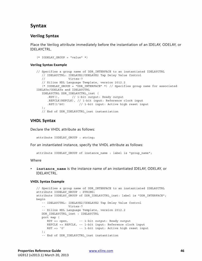
HIODELAY_GROUPHIODELAY_GROUP groups IDELAYCTRL components to their associated IDELAY or ODELAY instances for proper placement and replication.
If you use HIODELAY_GROUP to assign a group name to an IDELAYCTRL, you need to also associate an IDELAY or ODELAY cell to the group using the same HIODELAY_GROUP property.
IMPORTANT: Each cell may only belong to one HIODELAY_GROUP.
The following example uses set_property to group all the IDELAY/ODELAY elements associated with a specif ic IDELAYCTRL.
set_property HIODELAY_GROUP IO_DLY1 [get_cells MY_IDELAYCTRL_inst]set_property HIODELAY_GROUP IO_DLY1 [get_cells MY_IDELAY_inst]set_property HIODELAY_GROUP IO_DLY1 [get_cells MY_ODELAY_inst]
Difference Between HIODELAY_GROUP and IODELAY_GROUPHIODELAY_GROUP is uniquif ied per hierarchy. Use HIODELAY_GROUP when:
• You expect to have multiple instances of a module that contains an IDELAYCTRL.
and
• You do not intend to group that instance with any IDELAY or ODELAY instances in other logical hierarchies.
Architecture SupportAll architectures
Applicable Elements• Cells (get_cells)
° IDELAY, ODELAY, or IDELAYCTRL instances
ValuesAny specif ied group name

Properties Reference Guide www.xilinx.com 30UG912 (v2013.1) March 20, 2013
Syntax
Verilog Syntax
Place the Verilog attribute immediately before the instantiation of an IDELAY, ODELAY, or IDELAYCTRL.
(* HIODELAY_GROUP = "value" *)
Verilog Syntax Example
// Specifies a group name of DDR_INTERFACE to an instantiated IDELAYCTRL // IDELAYCTRL: IDELAYE2/ODELAYE2 Tap Delay Value Control // Virtex-7 // Xilinx HDL Language Template, version 2012.2 (* HIODELAY_GROUP = “DDR_INTERFACE” *) // Specifies group name for associated IDELAYs/ODELAYs and IDELAYCTRL IDELAYCTRL DDR_IDELAYCTRL_inst ( .RDY(), // 1-bit output: Ready output .REFCLK(REFCLK), // 1-bit input: Reference clock input .RST(1’b0) // 1-bit input: Active high reset input ); // End of DDR_IDELAYCTRL_inst instantiation
VHDL Syntax
Declare the VHDL attribute as follows:
attribute HIODELAY_GROUP : string;
For an instantiated instance, specify the VHDL attribute as follows:
attribute HIODELAY_GROUP of instance_name : label is "group_name";
Where
• instance_name is the instance name of an instantiated IDELAY, ODELAY, or IDELAYCTRL.
VHDL Syntax Example
// Specifies a group name of DDR_INTERFACE to an instantiated IDELAYCTRLattribute HIODELAY_GROUP : STRING;attribute HIODELAY_GROUP of DDR_IDELAYCTRL_inst: label is "DDR_INTERFACE";begin -- IDELAYCTRL: IDELAYE2/ODELAYE2 Tap Delay Value Control -- Virtex-7 -- Xilinx HDL Language Template, version 2012.2 DDR_IDELAYCTRL_inst : IDELAYCTRL port map ( RDY => open, -- 1-bit output: Ready output REFCLK => REFCLK, -- 1-bit input: Reference clock input RST => ‘0’ -- 1-bit input: Active high reset input ); -- End of DDR_IDELAYCTRL_inst instantiation

Properties Reference Guide www.xilinx.com 31UG912 (v2013.1) March 20, 2013
XDC Syntax
set_property HIODELAY_GROUP group_name [get_cells instance_name]
Where
• instance_name is the instance name of an IDELAY, ODELAY, or IDELAYCTRL.
XDC Syntax Example
# Specifies a group name of DDR_INTERFACE to an instantiated IDELAYCTRLset_property HIODELAY_GROUP DDR_INTERFACE [get_cells DDR_IDELAYCTRL_inst]
Note: When this property is set in both HDL code and in XDC, the XDC property takes precedence.
Affected Stepsplace_design
See Also• IODELAY_GROUP
• IDELAYCTRL
• IDELAYE2
• ODELAYE2

Properties Reference Guide www.xilinx.com 32UG912 (v2013.1) March 20, 2013
HLUTNMHLUTNM instructs the tool to place two LUT5, SRL16, or LUTRAM components with compatible inputs into the same LUT6 site. Specify the HLUTNM in pairs per hierarchy, with two of these specif ied on compatible instance types with the same group name.
Difference Between HLUTNM and LUTNMHLUTNM is uniquified per hierarchy.
• Use HLUTNM when you expect to have multiple instances of a module that contains LUT components to be grouped together.
• Use LUTNM to group two LUT components that exist in different hierarchies.
Architecture SupportAll architectures
Applicable Elements• Cells (get_cells)
° LUT (LUT1, LUT2, LUT3, LUT4, LUT5)
° SRL (SRL16E)
° LUTRAM (RAM32X1D, RAM32X1S)
ValuesA unique group name
Syntax
Verilog Syntax
Place the Verilog attribute immediately before the instantiation of a LUT.
The Verilog attribute must be used in pairs in the same logical hierarchy.
(* HLUTNM = "group_name" *)
Properties Reference Guide www.xilinx.com 33UG912 (v2013.1) March 20, 2013
Verilog Syntax Example
// Designates state0_inst to be placed in same LUT6 as state1_inst // LUT5: 5-input Look-Up Table with general output (Mapped to a LUT6) // Virtex-7 // Xilinx HDL Language Template, version 2012.2 (* HLUTNM = "LUT_group1" *) LUT5 #( .INIT(32'ha2a2aea2) // Specify LUT Contents ) state0_inst ( .O(state_out[0]), // LUT general output .I0(state_in[0]), // LUT input .I1(state_in[1]), // LUT input .I2(state_in[2]), // LUT input .I3(state_in[3]), // LUT input .I4(state_in[4]) // LUT input ); // End of state0_inst instantiation // LUT5: 5-input Look-Up Table with general output (Mapped to a LUT6) // Virtex-7 // Xilinx HDL Language Template, version 2012.2 (* HLUTNM = "LUT_group1" *) LUT5 #( .INIT(32'h00330073) // Specify LUT Contents ) state1_inst ( .O(state_out[1]), // LUT general output .I0(state_in[0]), // LUT input .I1(state_in[1]), // LUT input .I2(state_in[2]), // LUT input .I3(state_in[3]), // LUT input .I4(state_in[4]) // LUT input ); // End of state1_inst instantiation
VHDL Syntax
Declare the VHDL attribute as follows:
attribute HLUTNM : string;
For an instantiated instance, specify the VHDL attribute as follows:
attribute HLUTNM of instance_name : label is "group_name";
Where
• instance_name is a LUT1, LUT2, LUT3, LUT4, LUT5, SRL16, or LUTRAM instance.
The VHDL attribute must be used in pairs in the same logical hierarchy.

Properties Reference Guide www.xilinx.com 34UG912 (v2013.1) March 20, 2013
VHDL Syntax Example
-- Designates state0_inst to be placed in same LUT6 as state1_instattribute HLUTNM : string;attribute HLUTNM of state0_inst : label is "LUT_group1";attribute HLUTNM of state1_inst : label is "LUT_group1";begin -- LUT5: 5-input Look-Up Table with general output (Mapped to SliceM LUT6) -- Virtex-7 -- Xilinx HDL Language Template, version 2012.2 state0_inst : LUT5 generic map ( INIT => X"a2a2aea2") -- Specify LUT Contents port map ( O => state_out(0), -- LUT general output I0 => state_in(0), -- LUT input I1 => state_in(1), -- LUT input I2 => state_in(2), -- LUT input I3 => state_in(3), -- LUT input I4 => state_in(4) -- LUT input ); -- End of state0_inst instantiation -- LUT5: 5-input Look-Up Table with general output (Mapped to SliceM LUT6) -- Virtex-7 -- Xilinx HDL Language Template, version 2012.2 State1_inst : LUT5 generic map ( INIT => X"00330073") -- Specify LUT Contents port map ( O => state_out(1), -- LUT general output I0 => state_in(0), -- LUT input I1 => state_in(1), -- LUT input I2 => state_in(2), -- LUT input I3 => state_in(3), -- LUT input I4 => state_in(4) -- LUT input ); -- End of state1_inst instantiation
XDC Syntax
set_property HLUTNM group_name [get_cells instance_name]
Where
• instance_name is a LUT1, LUT2, LUT3, LUT4, LUT5, SRL16, or LUTRAM instance.
XDC Syntax Example
# Designates state0_inst LUT5 to be placed in same LUT6 as state1_instset_property HLUTNM LUT_group1 [get_cells state0_inst]set_property HLUTNM LUT_group1 [get_cells state1_inst]
Note: When this property is set in both HDL code and in XDC, the XDC property takes precedence.

Properties Reference Guide www.xilinx.com 35UG912 (v2013.1) March 20, 2013
Affected Stepsplace_design
See AlsoLUTNM

Properties Reference Guide www.xilinx.com 36UG912 (v2013.1) March 20, 2013
IN_TERMIN_TERM specif ies an un-calibrated input termination impedance value. IN_TERM is supported on High Range (HR) bank inputs only. For inputs in High Performance (HP) banks, specify a digitally controlled impedance (DCI) IOSTANDARD for on-chip termination.
The termination is present constantly on inputs, and on bidirectional pins whenever the output buffer is 3-stated. However, an important difference between this un-calibrated split-termination option and the 3-state split-termination DCI is that instead of calibrating to external reference resistors on the VRN and VRP pins when using DCI, this feature invokes internal resistors that have no calibration routine to compensate for temperature, process, or voltage variations. This option has target Thevenin equivalent resistance values of 40Ω, 50Ω, and 60Ω. For more information refer to the 7 Series FPGAs SelectIO Resources User Guide (UG471) [Ref 3].
Architecture SupportAll architectures on High Range (HR) bank inputs only.
Applicable Elements• Ports (get_ports)
° Input or bidirectional ports connected.
• Cells (get_cells)
° Input Buffers (all IBUF variants).
Values• NONE (default)
• TUNED_SPLIT
• UNTUNED_SPLIT_25
• UNTUNED_SPLIT_40
• UNTUNED_SPLIT_50
• UNTUNED_SPLIT_60
• UNTUNED_SPLIT_75
Properties Reference Guide www.xilinx.com 37UG912 (v2013.1) March 20, 2013
Syntax
Verilog Syntax
To set this attribute, place the proper Verilog attribute syntax before the top-level output port declaration.
(* IN_TERM = "{NONE|UNTUNED_SPLIT_40|UNTUNED_SPLIT_50|UNTUNED_SPLIT_60}" *)
Verilog Syntax Example
// Sets an on-chip input impedance of 50 Ohms to input ACT5(* IN_TERM = "UNTUNED_SPLIT_50" *) input ACT5,
VHDL Syntax
To set this attribute, place the proper VHDL attribute syntax before the top-level output port declaration.
Declare the VHDL attribute as follows:
attribute IN_TERM : string;
Specify the VHDL attribute as follows:
attribute IN_TERM of port_name : signal is value;
Where
• port_name is a top-level output port.
VHDL Syntax Example
ACT5 : in std_logic;attribute IN_TERM : string;-- Sets an on-chip input impedance of 50 Ohms to input ACT5attribute IN_TERM of ACT5 : signal is “UNTUNED_SPLIT_50”;
XDC Syntax
set_property IN_TERM value [get_ports port_name]
Where:
• IN_TERM can be assigned to port objects, and nets connected to port objects.
• port_name is an output or bidirectional port.

Properties Reference Guide www.xilinx.com 38UG912 (v2013.1) March 20, 2013
XDC Syntax Example
# Sets an on-chip input impedance of 50 Ohms to input ACT5set_property IN_TERM UNTUNED_SPLIT_50 [get_ports ACT5]
Note: When this property is set in both HDL code and in XDC, the XDC property takes precedence.
Affected Steps• I/O Planning
• Report Noise
• Report Power
See AlsoDIFF_TERM
DIFF_TERM
OUT_TERM

Properties Reference Guide www.xilinx.com 39UG912 (v2013.1) March 20, 2013
INTERNAL_VREFINTERNAL_VREF specif ies the use of an internal regulator on a bank to supply the voltage reference for standards requiring a reference voltage.
Architecture SupportAll architectures
Applicable Elements• I/O Bank (get_iobanks)
Values• 0.60
• 0.675
• 0.75
• 0.90
Syntax
Verilog Syntax
Not applicable
VHDL Syntax
Not applicable
XDC Syntax
set_property INTERNAL_VREF {value} [get_iobanks bank]
Where
• value is the reference voltage value.
XDC Syntax Example
# Designate Bank 14 to have a reference voltage of 0.75 Voltsset_property INTERNAL_VREF 0.75 [get_iobanks 14]
Properties Reference Guide www.xilinx.com 40UG912 (v2013.1) March 20, 2013
Affected Steps• I/O planning
• place_design
• DRC
• report_power
Properties Reference Guide www.xilinx.com 41UG912 (v2013.1) March 20, 2013
IOBIOB directs the tool to place a register in the input or output logic (I/O Block) to improve I/O timing.
Architecture SupportAll architectures
Applicable Elements• Ports (get_ports)
° Any port connected to a register
• Cells (get_cells)
° Registers connected directly to a top-level port
Values• FALSE (default)
• TRUE
Syntax
Verilog Syntax
To set this attribute, place the proper Verilog attribute syntax before the top-level output port declaration.
(* IOB = "{TRUE|FALSE}" *)
Verilog Syntax Example
// Place the register connected to ACK in the input logic site(* IOB = "TRUE" *) input ACK,
Alternative Verilog Syntax Example
The IOB attribute can be placed on an instantiated or inferred register connected to a top-level port.
Place the register connected to ACK in the input logic site.input ACK;(* IOB = “TRUE” *) reg ack_reg = 1’b0;always @(posedge CLK) ack_reg = 1’b0;

Properties Reference Guide www.xilinx.com 42UG912 (v2013.1) March 20, 2013
VHDL Syntax
To set this attribute, place the proper VHDL attribute syntax before the top-level output port declaration.
Declare the VHDL attribute as follows:
attribute IOB : string;
Specify the VHDL attribute as follows:
attribute IOB of <port_name>: signal is "{TRUE|FALSE}";
Where
• port_name is a top-level output port.
VHDL Syntax Example
ACK : in std_logic;attribute IOB : string;-- Place the register connected to ACK in the input logic siteattribute IOB of ACK: signal is "TRUE";
Alternative VHDL Syntax Example
The IOB attribute can be placed on an instantiated or inferred register connected to a top-level port. Place the register connected to ACK in the input logic site.
XDC Syntax
set_property IOB value [get_ports port_name]
Where
• value is TRUE or FALSE.
XDC Syntax Example
# Place the register connected to ACK in the input logic siteset_property IOB TRUE [get_ports ACK]
Note: When this property is set in both HDL code and in XDC, the XDC property takes precedence.
Affected Steps• place_design
Properties Reference Guide www.xilinx.com 43UG912 (v2013.1) March 20, 2013
IOBDELAYThe Input Output Block Delay (IOBDELAY) property sets the tap delay value of an IDELAY or IODELAY delay line cell. It specifies how the input path delay elements are to be programmed.
There are two possible destinations for input signals:
• The local IOB input FF
• A load external to the IOB
Xilinx devices allow a delay element to delay the signal going to one or both of these destinations.
Architecture SupportAll architectures
Applicable Elements• I/O Buffers (get_cells)
• Nets (get_nets)
Values• NONE: Sets the delay to OFF for both the IBUF and IFD paths.
• IBUF
° Sets the delay to OFF for any register inside the I/O component.
° Sets the delay to ON for the registers outside of the component if the input buffer drives a register D pin outside of the I/O component.
• IFD
° Sets the delay to ON for any register inside the I/O component.
° Sets the delay to OFF for the registers outside the component if a register occupies the input side of the I/O component, regardless of whether the register has the IOB=TRUE constraint.
• BOTH: Sets the delay to ON for both the IBUF and IFD paths.

Properties Reference Guide www.xilinx.com 44UG912 (v2013.1) March 20, 2013
Syntax
Verilog Syntax
Place the Verilog constraint immediately before the module or instantiation.
Specify the Verilog constraint as follows:
(* IOBDELAY = {NONE|BOTH|IBUF|IFD} *)
VHDL Syntax
Declare the VHDL constraint as follows:
attribute iobdelay: string;
Specify the VHDL constraint as follows:
attribute iobdelay of {component_name |label_name }: {component|label} is “{NONE|BOTH|IBUF|IFD}”;
XDC Syntax
set_property IOBDELAY value [get_cells cell_name]
Where:
• value is one of NONE, IBUF, IFD, BOTH
XDC Syntax Example
set_property IOBDELAY NONE [get_nets b[0]]
Note: You cannot set IOBDELAY on ports. However, you can set IOBDELAY on cells such as input buffers
Affected Steps• Timing
• Placement
• Routing
See Also

Properties Reference Guide www.xilinx.com 45UG912 (v2013.1) March 20, 2013
IODELAY_GROUPIODELAY_GROUP groups IDELAYCTRL cells together with their associated IDELAY and ODELAY cells to allow proper placement and replication.
If you use IODELAY_GROUP to assign a group name to an IDELAYCTRL, you need to also associate an IDELAY or ODELAY cell to the group using the same IODELAY_GROUP property.
IMPORTANT: Each cell may only belong to one IODELAY_GROUP.
The following example uses set_property to group all the IDELAY/ODELAY elements associated with a specif ic IDELAYCTRL.
set_property IODELAY_GROUP IO_DLY1 [get_cells MY_IDELAYCTRL_inst]set_property IODELAY_GROUP IO_DLY1 [get_cells MY_IDELAY_inst]set_property IODELAY_GROUP IO_DLY1 [get_cells MY_ODELAY_inst]
Difference Between IODELAY_GROUP and HIODELAY_GROUP IODELAY_GROUP can group elements across different hierarchies. Use IODELAY_GROUP to group I/O delay components in different hierarchies together.
HIODELAY_GROUP groups I/O delay components under the same hierarchical module.
Architecture SupportAll architectures
Applicable Elements• Cells (get_cells)
° IDELAY, ODELAY, or IDELAYCTRL instances
ValuesAny specif ied group name
Properties Reference Guide www.xilinx.com 46UG912 (v2013.1) March 20, 2013
Syntax
Verilog Syntax
Place the Verilog attribute immediately before the instantiation of an IDELAY, ODELAY, or IDELAYCTRL.
(* IODELAY_GROUP = "value" *)
Verilog Syntax Example
// Specifies a group name of DDR_INTERFACE to an instantiated IDELAYCTRL // IDELAYCTRL: IDELAYE2/ODELAYE2 Tap Delay Value Control // Virtex-7 // Xilinx HDL Language Template, version 2012.2 (* IODELAY_GROUP = “DDR_INTERFACE” *) // Specifies group name for associated IDELAYs/ODELAYs and IDELAYCTRL IDELAYCTRL DDR_IDELAYCTRL_inst ( .RDY(), // 1-bit output: Ready output .REFCLK(REFCLK), // 1-bit input: Reference clock input .RST(1’b0) // 1-bit input: Active high reset input ); // End of DDR_IDELAYCTRL_inst instantiation
VHDL Syntax
Declare the VHDL attribute as follows:
attribute IODELAY_GROUP : string;
For an instantiated instance, specify the VHDL attribute as follows:
attribute IODELAY_GROUP of instance_name : label is "group_name";
Where
• instance_name is the instance name of an instantiated IDELAY, ODELAY, or IDELAYCTRL.
VHDL Syntax Example
// Specifies a group name of DDR_INTERFACE to an instantiated IDELAYCTRLattribute IODELAY_GROUP : STRING;attribute IODELAY_GROUP of DDR_IDELAYCTRL_inst: label is "DDR_INTERFACE";begin -- IDELAYCTRL: IDELAYE2/ODELAYE2 Tap Delay Value Control -- Virtex-7 -- Xilinx HDL Language Template, version 2012.2 DDR_IDELAYCTRL_inst : IDELAYCTRL port map ( RDY => open, -- 1-bit output: Ready output REFCLK => REFCLK, -- 1-bit input: Reference clock input RST => ‘0’ -- 1-bit input: Active high reset input ); -- End of DDR_IDELAYCTRL_inst instantiation
Properties Reference Guide www.xilinx.com 47UG912 (v2013.1) March 20, 2013
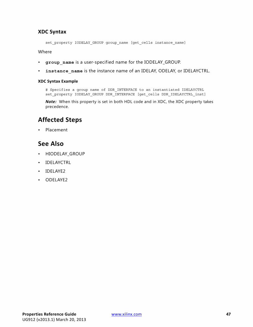
XDC Syntax
set_property IODELAY_GROUP group_name [get_cells instance_name]
Where
• group_name is a user-specif ied name for the IODELAY_GROUP.
• instance_name is the instance name of an IDELAY, ODELAY, or IDELAYCTRL.
XDC Syntax Example
# Specifies a group name of DDR_INTERFACE to an instantiated IDELAYCTRLset_property IODELAY_GROUP DDR_INTERFACE [get_cells DDR_IDELAYCTRL_inst]
Note: When this property is set in both HDL code and in XDC, the XDC property takes precedence.
Affected Steps• Placement
See Also• HIODELAY_GROUP
• IDELAYCTRL
• IDELAYE2
• ODELAYE2

Properties Reference Guide www.xilinx.com 48UG912 (v2013.1) March 20, 2013
IOSTANDARDIOSTANDARD specif ies which programmable I/O Standard to use to configure input, output, or bidirectional ports. You must specify an IOSTANDARD on all ports in order to create a bitstream.
Architecture SupportAll architectures
Applicable Elements• Ports (get_ports)
° Any port
• Cells (get_cells)
° I/O Buffers (all IBUF, OBUF, and IOBUF variants)
ValuesA valid I/O Standard for the target Xilinx FPGA. Refer to the 7 Series FPGAs SelectIO Resources User Guide (UG471) [Ref 3].
Syntax
Verilog Syntax
To set this attribute when inferring I/O buffers, place the proper Verilog attribute syntax before the top-level output port declaration.
(* IOSTANDARD = "value" *)
Verilog Syntax Example
// Sets the I/O Standard on the STATUS output to LVCMOS12(* IOSTANDARD = "LVCMOS12" *) output STATUS,
Alternative Verilog Syntax Example
If the I/O buffer is instantiated, IOSATNDARD can be set by assigning the IOSTANDARD parameter on the instantiated I/O buffer.
RECOMMENDED: Use the instantiation template from the Language Templates or the Vivado Design Suite 7 Series FPGA Libraries Guide (UG953) [Ref 1] to specify the proper syntax.

Properties Reference Guide www.xilinx.com 49UG912 (v2013.1) March 20, 2013
The following example sets the I/O Standard on the STATUS output to LVCMOS12.
// OBUF: Single-ended Output Buffer // Virtex-7 // Xilinx HDL Language Template, version 2012.2OBUF #( .DRIVE(12), // Specify the output drive strength .IOSTANDARD("LVCMOS12"), // Specify the output I/O standard .SLEW("SLOW") // Specify the output slew rate ) status_obuf ( .O(STATUS), // Buffer output (connect directly to top-level port) .I(status_int) // Buffer input );// End of status_obuf instantiation
VHDL Syntax
To set this attribute when inferring I/O buffers, place the proper VHDL attribute syntax before the top-level output port declaration.
Declare the VHDL attribute as follows:
attribute IOSTANDARD : string;
Specify the VHDL attribute as follows:
attribute IOSTANDARD of <port_name>: signal is "<standard>";
Where
• port_name is a top-level output port.
VHDL Syntax Example
STATUS : out std_logic;attribute IOSTANDARD : string;-- Sets the I/O Standard on the STATUS output to LVCMOS12attribute IOSTANDARD of STATUS: signal is "LVCMOS12";
Properties Reference Guide www.xilinx.com 50UG912 (v2013.1) March 20, 2013
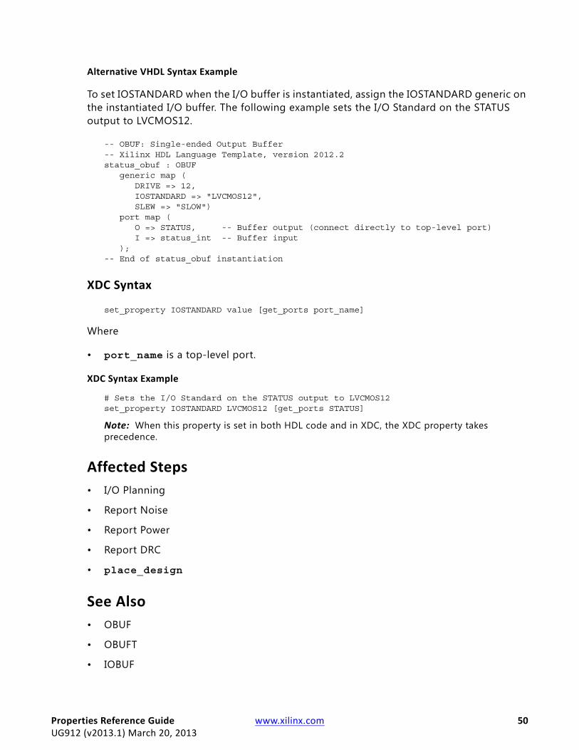
Alternative VHDL Syntax Example
To set IOSTANDARD when the I/O buffer is instantiated, assign the IOSTANDARD generic on the instantiated I/O buffer. The following example sets the I/O Standard on the STATUS output to LVCMOS12.
-- OBUF: Single-ended Output Buffer-- Xilinx HDL Language Template, version 2012.2status_obuf : OBUF generic map ( DRIVE => 12, IOSTANDARD => "LVCMOS12", SLEW => "SLOW") port map ( O => STATUS, -- Buffer output (connect directly to top-level port) I => status_int -- Buffer input );-- End of status_obuf instantiation
XDC Syntax
set_property IOSTANDARD value [get_ports port_name]
Where
• port_name is a top-level port.
XDC Syntax Example
# Sets the I/O Standard on the STATUS output to LVCMOS12set_property IOSTANDARD LVCMOS12 [get_ports STATUS]
Note: When this property is set in both HDL code and in XDC, the XDC property takes precedence.
Affected Steps• I/O Planning
• Report Noise
• Report Power
• Report DRC
• place_design
See Also• OBUF
• OBUFT
• IOBUF

Properties Reference Guide www.xilinx.com 51UG912 (v2013.1) March 20, 2013
KEEP_HIERARCHYKEEP_HIERARCHY directs the tool to retain a user hierarchy so that optimization does not occur across its boundary. While this can assist floorplanning, analysis, and debugging, it may inhibit optimization, resulting in a larger, slower design.
RECOMMENDED: To avoid these negative effects, register all outputs of a module instance in which a KEEP_HIERARCHY is attached. To be most effective, apply this attribute before synthesis.
Architecture SupportAll
Applicable Elements• Cells (get_cells)
° User defined instance
Values• FALSE (default)
Allows optimization across the hierarchy.
• TRUE
Preserves the hierarchy by not allowing optimization across the hierarchy boundary.
Syntax
Verilog Syntax
Place the Verilog attribute immediately before the user hierarchy instantiation:
(* KEEP_HIERARCHY = "{TRUE|FALSE}" *)
Verilog Syntax Example
// Preserve the hierarchy of instance CLK1_rst_sync(* KEEP_HIERARCHY = "TRUE" *) reset_sync #( .STAGES(5) ) CLK1_rst_sync ( .RST_IN(RST | ~LOCKED), .CLK(clk1_100mhz), .RST_OUT(rst_clk1) );
Properties Reference Guide www.xilinx.com 52UG912 (v2013.1) March 20, 2013
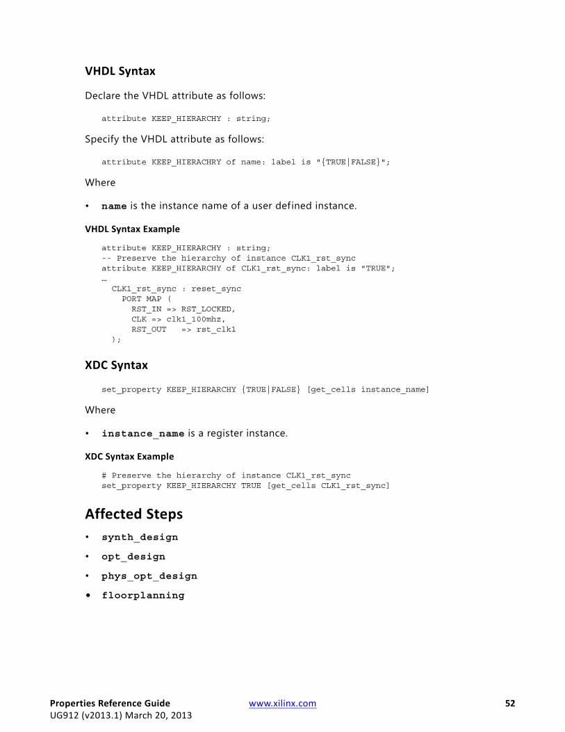
VHDL Syntax
Declare the VHDL attribute as follows:
attribute KEEP_HIERARCHY : string;
Specify the VHDL attribute as follows:
attribute KEEP_HIERACHRY of name: label is "{TRUE|FALSE}";
Where
• name is the instance name of a user defined instance.
VHDL Syntax Example
attribute KEEP_HIERARCHY : string;-- Preserve the hierarchy of instance CLK1_rst_syncattribute KEEP_HIERARCHY of CLK1_rst_sync: label is "TRUE";… CLK1_rst_sync : reset_sync PORT MAP ( RST_IN => RST_LOCKED, CLK => clk1_100mhz, RST_OUT => rst_clk1 );
XDC Syntax
set_property KEEP_HIERARCHY {TRUE|FALSE} [get_cells instance_name]
Where
• instance_name is a register instance.
XDC Syntax Example
# Preserve the hierarchy of instance CLK1_rst_syncset_property KEEP_HIERARCHY TRUE [get_cells CLK1_rst_sync]
Affected Steps• synth_design
• opt_design
• phys_opt_design
• floorplanning

Properties Reference Guide www.xilinx.com 53UG912 (v2013.1) March 20, 2013
KEEPERKEEPER applies a weak driver on a tri-stateable output or bidirectional port to preserve its value when not being driven. The KEEPER property retains the value of the output net to which it is attached.
For example, if logic 1 is being driven onto a net, KEEPER drives a weak or resistive 1 onto the net. If the net driver is then tri-stated, KEEPER continues to drive a weak or resistive 1 onto the net to preserve that value.
Input buffers (e.g., IBUF), 3-state output buffers (e.g., OBUFT), and bidirectional buffers (e.g., IOBUF) can have a weak pull-up resistor, a weak pull-down resistor, or a weak “keeper” circuit. This feature can be invoked by adding the one of the following properties to the net object connected to the buffer:
• PULLUP
• PULLDOWN
• KEEPER
Architecture SupportAll
Applicable Elements• Nets connected to I/O Buffers (get_nets)
Values• TRUE | YES: Use a keeper circuit to preserve the value on the net.
• FALSE | NO: Do not use a keeper circuit. Default.

Properties Reference Guide www.xilinx.com 54UG912 (v2013.1) March 20, 2013
Syntax
Verilog Syntax
Place the Verilog constraint immediately before the module or instantiation.
Specify the Verilog constraint as follows:
(* KEEPER = " {YES|NO|TRUE|FALSE}" *)
VHDL Syntax
Declare the VHDL constraint as follows:
attribute keeper: string;
Specify the VHDL constraint as follows:
attribute keeper of signal_name : signal is “{YES|NO|TRUE|FALSE}”;
XDC Syntax
set_property KEEPER {TRUE|FALSE} [get_nets net_name]
Where
• net_name is the name of a net connected to an IBUF, OBUFT, or IOBUF cell.
XDC Syntax Example
# Use a keeper circuit to preserve the value on the specified netset_property KEEPER true [get_nets n1]
Note: When this property is set in both HDL code and in XDC, the XDC property takes precedence.
Affected Steps
See AlsoKEEPER
PULLDOWN
PULLUP

Properties Reference Guide www.xilinx.com 55UG912 (v2013.1) March 20, 2013
LOCLOC specif ies a specif ic placement of a primitive component within the device.
Architecture SupportAll architectures
Applicable Elements• Cells (get_cells)
° Any primitive cell
ValuesSite name (for example, SLICE_X15Y14 or RAMB18_X6Y9)
Syntax
Verilog Syntax
Place the Verilog attribute immediately before the instantiation of a component.
The Verilog attribute can also be placed before the reg declaration of an inferred register, SRL, or LUTRAM when that reg can be placed into a single device site:
(* LOC = "site_name" *)// Designates placed_reg to be placed in Slice site SLICE_X0Y0(* LOC = "SLICE_X0Y0" *) reg placed_reg;
VHDL Syntax
Declare the VHDL attribute as follows:
attribute LOC : string;
For an instantiated instance, specify the VHDL attribute as follows:
attribute LOC of instance_name : label is "site_name";

Properties Reference Guide www.xilinx.com 56UG912 (v2013.1) March 20, 2013
Where
• instance_name is the instance name of an instantiated primitive.
VHDL Syntax Example
-- Designates instantiated register instance placed_reg to be placed-- in Slice site SLICE_X0Y0attribute LOC of placed_reg : label is "SLICE_X0Y0";
For an inferred instance, specify the VHDL attribute as follows:
attribute LOC of signal_name : signal is "site_name";
Where
• signal_name is the signal name of an inferred primitive that can be placed into a single site.
VHDL Syntax Example
-- Designates inferred register placed_reg to be placed in Slice site SLICE_X0Y0attribute LOC of placed_reg : signal is "SLICE_X0Y0";
XDC Syntax
set_property LOC site_name [get_cells instance_name]
Where
• instance_name is a primitive instance.
XDC Syntax Example
# Designates placed_reg to be placed in Slice site SLICE_X0Y0set_property LOC SLICE_X0Y0 [get_cells placed_reg]
Note: When this property is set in both HDL code and in XDC, the XDC property takes precedence.
Affected Steps• Design Floorplanning
• place_design
See Also• BEL
• PACKAGE_PIN
Properties Reference Guide www.xilinx.com 57UG912 (v2013.1) March 20, 2013
LUTNMLUTNM instructs the tool to place two LUT5, SRL16, or LUTRAM components with compatible inputs into the same LUT6 site. The LUTNM must be specified in pairs, with two of these specif ied on compatible instance types with the same group name.
Difference Between LUTNM and HLUTNM HLUTNM can be used to combine two LUT components that exist in different user hierarchy. Use LUTNM to group two LUT components that exist in the same user hierarchy.
Architecture SupportAll architectures
Applicable Elements• Cells (get_cells)
° LUT (LUT1, LUT2, LUT3, LUT4, LUT5)
° SRL (SRL16E)
° LUTRAM (RAM32X1D, RAM32X1S)
ValuesA unique group name
Syntax
Verilog Syntax
Place the Verilog attribute immediately before the instantiation of a LUT. The Verilog attribute must be used in pairs in the same logical hierarchy.
(* LUTNM = "group_name" *)

Properties Reference Guide www.xilinx.com 58UG912 (v2013.1) March 20, 2013
Verilog Syntax Example
// Designates state0_inst to be placed in same LUT6 as state1_inst // LUT5: 5-input Look-Up Table with general output (Mapped to a LUT6) // Virtex-7 // Xilinx HDL Language Template, version 2012.2 (* LUTNM = "LUT_group1" *) LUT5 #( .INIT(32'ha2a2aea2) // Specify LUT Contents ) state0_inst ( .O(state_out[0]), // LUT general outpu .I0(state_in[0]), // LUT input .I1(state_in[1]), // LUT input .I2(state_in[2]), // LUT input .I3(state_in[3]), // LUT input .I4(state_in[4]) // LUT input ); // End of state0_inst instantiation // LUT5: 5-input Look-Up Table with general output (Mapped to a LUT6) // Virtex-7 // Xilinx HDL Language Template, version 2012.2 (* LUTNM = "LUT_group1" *) LUT5 #( .INIT(32'h00330073) // Specify LUT Contents ) state1_inst ( .O(state_out[1]), // LUT general output .I0(state_in[0]), // LUT input .I1(state_in[1]), // LUT input .I2(state_in[2]), // LUT input .I3(state_in[3]), // LUT input .I4(state_in[4]) // LUT input ); // End of state1_inst instantiation
VHDL Syntax
Declare the VHDL attribute as follows:
attribute LUTNM : string;
For an instantiated instance, specify the VHDL attribute as follows:
attribute LUTNM of instance_name : label is "group_name";
Where
• instance_name is a LUT1, LUT2, LUT3, LUT4, LUT5, SRL16, or LUTRAM instance.
The VHDL attribute must be used in pairs in the same logical hierarchy.

Properties Reference Guide www.xilinx.com 59UG912 (v2013.1) March 20, 2013
VHDL Syntax Example
-- Designates state0_inst to be placed in same LUT6 as state1_instattribute LUTNM : string;attribute LUTNM of state0_inst : label is "LUT_group1";attribute LUTNM of state1_inst : label is "LUT_group1";begin -- LUT5: 5-input Look-Up Table with general output (Mapped to SliceM LUT6) -- Virtex-7 -- Xilinx HDL Language Template, version 2012.2 state0_inst : LUT5 generic map ( INIT => X"a2a2aea2") -- Specify LUT Contents port map ( O => state_out(0), -- LUT general output I0 => state_in(0), -- LUT input I1 => state_in(1), -- LUT input I2 => state_in(2), -- LUT input I3 => state_in(3), -- LUT input I4 => state_in(4) -- LUT input ); -- End of state0_inst instantiation -- LUT5: 5-input Look-Up Table with general output (Mapped to SliceM LUT6) -- Virtex-7 -- Xilinx HDL Language Template, version 2012.2 State1_inst : LUT5 generic map ( INIT => X"00330073") -- Specify LUT Contents port map ( O => state_out(1), -- LUT general output I0 => state_in(0), -- LUT input I1 => state_in(1), -- LUT input I2 => state_in(2), -- LUT input I3 => state_in(3), -- LUT input I4 => state_in(4) -- LUT input ); -- End of state1_inst instantiation
XDC Syntax
set_property LUTNM group_name [get_cells instance_name]
Where
• instance_name is a LUT1, LUT2, LUT3, LUT4, LUT5, SRL16, or LUTRAM instance.
XDC Syntax Example
# Designates state0_inst LUT5 to be placed in same LUT6 as state1_instset_property LUTNM LUT_group1 [get_cells U1/state0_inst]set_property LUTNM LUT_group1 [get_cells U2/state1_inst]
Note: When this property is set in both HDL code and in XDC, the XDC property takes precedence.

Properties Reference Guide www.xilinx.com 60UG912 (v2013.1) March 20, 2013
Affected Stepsplace_design
See AlsoHLUTNM

Properties Reference Guide www.xilinx.com 61UG912 (v2013.1) March 20, 2013
MARK_DEBUGUse MARK_DEBUG to specify that a net should be debugged using the ChipScope™ tool. This may prevent optimization that may have otherwise occurred to that signal. However, it provides an easy means to later observe the values on this signal during FPGA operation.
Architecture SupportAll architectures
Applicable Elements• Nets (get_nets)
° Any net accessible to the internal array.
Note: Some nets may have dedicated connectivity or other aspects that prohibit visibility for debug purposes.
Values• TRUE
• FALSE
Syntax
Verilog Syntax
To set this attribute, place the proper Verilog attribute syntax before the top-level output port declaration:
(* MARK_DEBUG = "{TRUE|FALSE}" *)
Verilog Syntax Example
// Marks an internal wire for ChipScope debug(* MARK_DEBUG = "TRUE" *) wire debug_wire,

Properties Reference Guide www.xilinx.com 62UG912 (v2013.1) March 20, 2013
VHDL Syntax
To set this attribute, place the proper VHDL attribute syntax before the top-level output port declaration.
Declare the VHDL attribute as follows:
attribute MARK_DEBUG : string;
Specify the VHDL attribute as follows:
attribute MARK_DEBUG of signal_name : signal is “{TRUE|FALSE}”;
Where
• signal_name is an internal signal.
VHDL Syntax Example
signal debug_wire : std_logic;attribute MARK_DEBUG : string;-- Marks an internal wire for ChipScope debugattribute MARK_DEBUG of debug_wire : signal is “TRUE”;
XDC Syntax
set_property MARK_DEBUG value [get_nets net_name]
Where
• net_name is a signal name.
XDC Syntax Example
# Marks an internal wire for ChipScope debugset_property MARK_DEBUG TRUE [get_nets debug_wire]
Affected Steps• place_design
• ChipScope
See AlsoDONT_TOUCH

Properties Reference Guide www.xilinx.com 63UG912 (v2013.1) March 20, 2013
OUT_TERMOUT_TERM sets the configuration of the output termination resistance for an output port
OUT_TERM specifies an un-calibrated output termination impedance value. OUT_TERM is supported on High Range (HR) bank outputs only.
For outputs in High Performance (HP) banks, use Digital Controlled Impedance (DCI) circuits for on-chip termination. Refer to DCI_CASCADE and DCI_VALUE for more information.
Architecture SupportAll architectures on High Range (HR) bank inputs only
Applicable Elements• Ports (get_ports)
° Output or bidirectional ports connected
• Cells (get_cells)
° Output Buffers (all OBUF variants)
Values• NONE (default)
• TUNED
• UNTUNED_25
• UNTUNED_50
• UNTUNED_75
Syntax
Verilog Syntax
To set this attribute, place the proper Verilog attribute syntax before the top-level output port declaration.
(* OUT_TERM = "{NONE|TUNED|UNTUNED_SPLIT_25|UNTUNED_SPLIT_50|UNTUNED_SPLIT_75}" *)
Properties Reference Guide www.xilinx.com 64UG912 (v2013.1) March 20, 2013
Verilog Syntax Example
// Sets an on-chip input impedance of 50 Ohms to input ACT5(* OUT_TERM = "UNTUNED_SPLIT_50" *) input ACT5,
VHDL Syntax
To set this attribute, place the proper VHDL attribute syntax before the top-level output port declaration. Declare the VHDL attribute as follows:
attribute OUT_TERM : string;
Specify the VHDL attribute as follows:
attribute OUT_TERM of port_name : signal is value;
Where
• port_name is a top-level output port.
VHDL Syntax Example
ACT5 : in std_logic;attribute OUT_TERM : string;-- Sets an on-chip input impedance of 50 Ohms to input ACT5attribute OUT_TERM of ACT5 : signal is “UNTUNED_SPLIT_50”;
XDC Syntax
set_property OUT_TERM value [get_ports port_name]
Where
• port_name is an output or bidirectional port.
XDC Syntax Example
# Sets an on-chip output impedance of 50 Ohms to output ACT5set_property OUT_TERM UNTUNED_SPLIT_50 [get_ports ACT5]
Note: When this property is set in both HDL code and in XDC, the XDC property takes precedence.
Affected Steps• I/O Planning
• report_noise
• report_power

Properties Reference Guide www.xilinx.com 65UG912 (v2013.1) March 20, 2013
PACKAGE_PINPACKAGE_PIN specif ies a specific placement of a top-level port in the logical design to a physical package pin on the device.
Architecture SupportAll architectures
Applicable Elements• Ports (get_ports)
° Any top-level port
ValuesPackage pin name
Syntax
Verilog Syntax
Place the Verilog attribute immediately before the port declaration:
(* PACKAGE_PIN = "pin_name" *)
Verilog Syntax Example
// Designates port CLK to be placed on pin B26(* PACKAGE_PIN = "B26" *) input CLK;
VHDL Syntax
Declare the VHDL attribute as follows:
attribute PACKAGE_PIN : string;
Specify the VHDL attribute as follows:
attribute PACKAGE_PIN of port_name : signal is "pin_name";
VHDL Syntax Example
-- Designates CLK to be placed on pin B26attribute PACKAGE_PIN of CLK : signal is "B26";

Properties Reference Guide www.xilinx.com 66UG912 (v2013.1) March 20, 2013
XDC Syntax
set_property PACKAGE_PIN pin_name [get_ports port_name]
XDC Syntax Example
# Designates CLK to be placed on pin B26set_property PACKAGE_PIN B26 [get_ports CLK]
Note: When this property is set in both HDL code and in XDC, the XDC property takes precedence.
Affected Steps• Pin planning
• place_design
See AlsoLOC

Properties Reference Guide www.xilinx.com 67UG912 (v2013.1) March 20, 2013
POST_CRCThe Post CRC (POST_CRC) constraint enables or disables the Cyclic Redundancy Check (CRC) error detection feature for configuration logic, allowing for notification of any possible change to the configuration memory.
Enabling the POST_CRC property controls the generation of a pre-computed CRC value in the bitstream. As the configuration data frames are loaded, the device calculates a Cyclic Redundancy Check (CRC) value from the configuration data packets. After the configuration data frames are loaded, the configuration bitstream can issue a Check CRC instruction to the device, followed by the pre-computed CRC value. If the CRC value calculated by the device does not match the expected CRC value in the bitstream, the device pulls INIT_B Low and aborts configuration. For more information refer to the 7 Series FPGA Configuration User Guide (UG470) [Ref 2].
When CRC is disabled a constant value is inserted in the bitstream in place of the CRC, and the device does not calculate a CRC.
Architecture Support• Artix-7
• Virtex-7
• Kintex-7
Applicable Elements• Design (current_design)
° The current implemented design.
Values• DISABLE: Disables the Post CRC checking feature (default).
• ENABLE: Enables the Post CRC checking feature.
Syntax
XDC Syntax
set_property POST_CRC ENABLE | DISABLE [current_design]
XDC Syntax Example
set_property POST_CRC Enable [current_design]
Properties Reference Guide www.xilinx.com 68UG912 (v2013.1) March 20, 2013
Affected Steps• write_bitstream
• launch_runs
See AlsoPOST_CRC_ACTION
POST_CRC_FREQ
POST_CRC_INIT_FLAG
POST_CRC_SOURCE

Properties Reference Guide www.xilinx.com 69UG912 (v2013.1) March 20, 2013
POST_CRC_ACTION The Post CRC Action property (POST_CRC_ACTION) applies to the configuration logic CRC error detection mode. This property determines the action that the device takes when a CRC mismatch is detected: correct the error, continue operation, or stop configuration.
During readback, the syndrome bits are calculated for every frame. If a single bit error is detected, the readback is stopped immediately. If correction is enabled using the POST_CRC_ACTION property, then the readback CRC logic performs correction on single bit errors. The frame in error is readback again, and using the syndrome information, the bit in error is fixed and written back to the frame. If the POST_CRC_ACTION is set to Correct_And_Continue, then the readback logic starts over from the first address. If the Correct_And_Halt option is set, the readback logic stops after correction. Refer to the 7 Series FPGA Configuration User Guide (UG470) [Ref 2].
This property is only applicable when POST_CRC is set to ENABLE.
Architecture Support• Artix-7
• Virtex-7
• Kintex-7
Applicable Elements• Design (current_design)
° The current implemented design.
Values• HALT: If a CRC mismatch is detected, stop reading back the bitstream, stop computing the
comparison CRC, and stop making the comparison against the pre-computed CRC.
• CONTINUE: If a CRC mismatch is detected by the CRC comparison, continue reading back the bitstream, computing the comparison CRC, and making the comparison against the pre-computed CRC.
• CORRECT_AND_CONTINUE: If a CRC mismatch is detected by the CRC comparison, it is corrected and continues reading back the bitstream, computing the comparison CRC, and making the comparison against the pre-computed CRC.
• CORRECT_AND_HALT: If a CRC mismatch is detected, it is corrected and stops reading back the bitstream, computing the comparison CRC, and making the comparison against the pre-computed CRC.
Properties Reference Guide www.xilinx.com 70UG912 (v2013.1) March 20, 2013
Syntax
XDC Syntax
set_property POST_CRC_ACTION <VALUE> [get_ports port_name]
Where:
• <VALUE> is one of the accepted values for the POST_CRC_ACTION property.
XDC Syntax Example
set_property POST_CRC_ACTION correct_and_continue [current_design]
Affected Steps• write_bitstream
• launch_runs
See AlsoPOST_CRC
POST_CRC_FREQ
POST_CRC_INIT_FLAG
POST_CRC_SOURCE

Properties Reference Guide www.xilinx.com 71UG912 (v2013.1) March 20, 2013
POST_CRC_FREQThe Post CRC Frequency property (POST_CRC_FREQ) controls the frequency with which the configuration CRC check is performed for the current design.
This property is only applicable when POST_CRC is set to ENABLE. Enabling the POST_CRC property controls the periodic comparison of a pre-computed CRC value in the bitstream with an internal CRC value computed by readback of the configuration memory cells.
The POST_CRC_FREQ defines the frequency in MHz of the readback function, with a default value of 1 MHz.
Architecture Support• Artix-7
• Virtex-7
• Kintex-7
Applicable Elements• Design (current_design)
° The current implemented design.
Values• Specify the frequency in MHz as an integer with one of the following accepted values:
° 1 2 3 4 6 7 8 10 12 13 16 17 22 25 26 27 33 40 44 50 66 100
° Default = 1 MHz
Syntax
XDC Syntax
set_property POST_CRC_FREQ <VALUE> [current_design]
Where:
• <VALUE> is one of the accepted values for the POST_CRC_FREQ property.
XDC Syntax Example
set_property POST_CRC_FREQ 50 [current_design]

Properties Reference Guide www.xilinx.com 72UG912 (v2013.1) March 20, 2013
Affected Steps• write_bitstream
• launch_runs
See AlsoPOST_CRC
POST_CRC_ACTION
POST_CRC_INIT_FLAG
POST_CRC_SOURCE

Properties Reference Guide www.xilinx.com 73UG912 (v2013.1) March 20, 2013
POST_CRC_INIT_FLAGThe Post CRC INIT Flag property (POST_CRC_INIT_FLAG) determines whether the INIT_B pin is enabled as an output for the SEU (Single Event Upset) error signal.
The error condition is always available from the FRAME_ECC site. However, when the POST_CRC_INIT_FLAG is ENABLED, which is the default, the INIT_B pin also flags the CRC error condition when it occurs.
This property is only applicable when POST_CRC is set to ENABLE.
Architecture Support• Artix-7
• Virtex-7
• Kintex-7
Applicable Elements• Design (current_design)
° The current implemented design.
Values• DISABLE: Disables the use of the INIT_B pin, with the FRAME_ECC site as the sole source
of the CRC error signal.
• ENABLE: Leaves the INIT_B pin enabled as a source of the CRC error signal. (Default)
Syntax
XDC Syntax
set_property POST_CRC_INIT_FLAG ENABLE | DISABLE [curent_design]
XDC Syntax Example
set_property POST_CRC_INIT_FLAG Enable [current_design]

Properties Reference Guide www.xilinx.com 74UG912 (v2013.1) March 20, 2013
Affected Steps• write_bitstream
• launch_runs
See AlsoPOST_CRC
POST_CRC_ACTION
POST_CRC_FREQ
POST_CRC_SOURCE

Properties Reference Guide www.xilinx.com 75UG912 (v2013.1) March 20, 2013
POST_CRC_SOURCEThe Post CRC Source (POST_CRC_SOURCE) constraint specifies the source of the CRC value when the configuration logic CRC error detection feature is used for notification of any possible change to the configuration memory.
This property is only applicable when POST_CRC is set to ENABLE.
Enabling the POST_CRC property controls the generation of a pre-computed CRC value in the bitstream. As the configuration data frames are loaded, the device calculates a Cyclic Redundancy Check (CRC) value from the configuration data packets. The POST_CRC_SOURCE property defines the expected CRC value as either coming from a pre-computed value, or as being taken from the configuration data in the first readback pass.
Architecture Support• Artix-7
• Virtex-7
• Kintex-7
Applicable Elements• Design (current_design)
° The current implemented design.
Values• PRE_COMPUTED: Determine an expected CRC value from the bitstream. (Default)
• FIRST_READBACK: Extract the actual CRC value from the first readback pass, to use for comparison with future readback iterations.

Properties Reference Guide www.xilinx.com 76UG912 (v2013.1) March 20, 2013
Syntax
XDC Syntax
set_property POST_CRC_SOURCE FIRST_READBACK | PRE_COMPUTED [current_design]
XDC Syntax Example
set_property POST_CRC_SOURCE PRE_COMPUTED [current_design]
Affected Steps• write_bitstream
• launch_runs
See AlsoPOST_CRC
POST_CRC_ACTION
POST_CRC_FREQ
POST_CRC_INIT_FLAG

Properties Reference Guide www.xilinx.com 77UG912 (v2013.1) March 20, 2013
PROHIBITPROHIBIT specif ies that a pin or site cannot be used for placement.
Architecture SupportAll architectures
Applicable Elements• Sites (get_sites)
• BELs (get_bels)
Values1
Syntax
Verilog Syntax
Not applicable
VHDL Syntax
Not applicable
XDC Syntax
set_property PROHIBIT 1 [get_sites site]
XDC Syntax Example
# Prohibit the use of package pin Y32set_property prohibit 1 [get_sites Y32]
Affected Steps• I/O planning
• place_design

Properties Reference Guide www.xilinx.com 78UG912 (v2013.1) March 20, 2013
PULLDOWNPULLDOWN applies a weak logic low level on a tri-stateable output or bidirectional port to prevent it from floating. The PULLDOWN property guarantees a logic Low level to allow tri-stated nets to avoid floating when not being driven.
Input buffers (e.g., IBUF), 3-state output buffers (e.g., OBUFT), and bidirectional buffers (e.g., IOBUF) can have a weak pull-up resistor, a weak pull-down resistor, or a weak “keeper” circuit. This feature can be invoked by adding the one of the following properties to the net object connected to the buffer:
• PULLUP
• PULLDOWN
• KEEPER
For more information see Vivado Design Suite 7 Series FPGA Libraries Guide (UG953) [Ref 1].
Architecture SupportAll
Applicable Elements• Nets connected to I/O Buffers (get_nets)
Values• TRUE | YES: Use a pulldown circuit to avoid signal floating when not being driven.
• FALSE | NO: Do not use a pulldown circuit. Default.
Syntax
Verilog Syntax
Place the Verilog attribute immediately before the module or instantiation. Specify as follows:
(* PULLDOWN = " {YES|NO|TRUE|FALSE}" *)

Properties Reference Guide www.xilinx.com 79UG912 (v2013.1) March 20, 2013
VHDL Syntax
Declare the VHDL attribute as follows:
attribute pulldown: string;
Specify the VHDL attribute as follows:
attribute pulldown of signal_name : signal is “{YES|NO|TRUE|FALSE}”;
XDC Syntax
set_property PULLDOWN {TRUE|FALSE} [get_nets net_name]
Where
• net_name is the name of a net connected to an IBUF, OBUFT, or IOBUF cell.
XDC Syntax Example
# Use a pulldown circuitset_property PULLDOWN true [get_nets n1]
Note: When this property is set in both HDL code and in XDC, the XDC property takes precedence.
Affected Steps
See AlsoKEEPER
PULLUP

Properties Reference Guide www.xilinx.com 80UG912 (v2013.1) March 20, 2013
PULLUPPULLUP applies a weak logic High on a tri-stateable output or bidirectional port to prevent it from floating. The PULLUP property guarantees a logic High level to allow tri-stated nets to avoid floating when not being driven.
Input buffers (e.g., IBUF), 3-state output buffers (e.g., OBUFT), and bidirectional buffers (e.g., IOBUF) can have a weak pull-up resistor, a weak pull-down resistor, or a weak “keeper” circuit. This feature can be invoked by adding the one of the following properties to the net object connected to the buffer:
• PULLUP
• PULLDOWN
• KEEPER
For more information see Vivado Design Suite 7 Series FPGA Libraries Guide (UG953) [Ref 1].
Architecture SupportAll
Applicable Elements• Nets connected to I/O Buffers (get_nets)
Values• TRUE | YES: Use a pullup circuit to avoid signal floating when not being driven.
• FALSE | NO: Do not use a pullup circuit. Default.
Syntax
Verilog Syntax
Place the Verilog attribute immediately before the module or instantiation. Specify as follows:
(* PULLUP = " {YES|NO|TRUE|FALSE}" *)

Properties Reference Guide www.xilinx.com 81UG912 (v2013.1) March 20, 2013
VHDL Syntax
Declare the VHDL attribute as follows:
attribute pullup: string;
Specify the VHDL attribute as follows:
attribute pullup of signal_name : signal is “{YES|NO|TRUE|FALSE}”;
XDC Syntax
set_property PULLUP {TRUE|FALSE} [get_nets net_name]
Where
• net_name is the name of a net connected to an IBUF, OBUFT, or IOBUF cell.
XDC Syntax Example
set_property PULLUP true [get_nets n1]
Note: When this property is set in both HDL code and in XDC, the XDC property takes precedence.
Affected Steps
See AlsoKEEPER
PULLDOWN

Properties Reference Guide www.xilinx.com 82UG912 (v2013.1) March 20, 2013
SLEWSLEW specif ies output buffer slew rate for output buffers configured with I/O standards that support programmable output slew rates.
Architecture SupportAll architectures
Applicable Elements• Ports (get_ports)
° Output or bidirectional ports connected
• Cells (get_cells)
° Output Buffers (all OBUF variants)
Values• SLOW (default)
• FAST
Syntax
Verilog Syntax
To set this attribute when inferring I/O buffers, place the proper Verilog attribute syntax before the top-level output port declaration.
(* DRIVE = "{SLOW|FAST}" *)
Verilog Syntax Example
// Sets the Slew rate to be FAST(* SLEW = "FAST" *) output FAST_DATA,
Alternative Verilog Syntax Example
To set SLEW when the output or bidirectional buffer is instantiated, assign the SLEW parameter on the instantiated output buffer.
RECOMMENDED: Use the instantiation template from the Language Templates or the Vivado Design Suite 7 Series FPGA Libraries Guide (UG953) [Ref 1] to specify the proper syntax.

Properties Reference Guide www.xilinx.com 83UG912 (v2013.1) March 20, 2013
The following example sets the slew rate on the OBUF instance named fast_data_obuf to FAST:
// OBUF: Single-ended Output Buffer // Virtex-7 // Xilinx HDL Language Template, version 2012.2OBUF #( .DRIVE(12), // Specify the output drive strength .IOSTANDARD("DEFAULT"), // Specify the output I/O standard .SLEW("FAST") // Specify the output slew rate ) fast_data_obuf ( .O(FAST_DATA), // Buffer output (connect directly to top-level port) .I(fast_data_int) // Buffer input );// End of fast_data_obuf instantiation
VHDL Syntax
To set this attribute when inferring I/O buffers, place the proper VHDL attribute syntax before the top-level output port declaration.
Declare the VHDL attribute as follows:
attribute SLEW : string;
Specify the VHDL attribute as follows:
attribute SLEW of port_name : signal is value;
Where
• port_name is a top-level output port.
VHDL Syntax Example
FAST_DATA : out std_logic;attribute SLEW : string;-- Sets the Slew rate to be FASTattribute SLEW of STATUS : signal is “FAST”;
Alternative VHDL Syntax Example
To set SLEW when the output or bidirectional buffer is instantiated, assign the SLEW generic on the instantiated output buffer.
RECOMMENDED: Use the instantiation template from the Language Templates or the Vivado Design Suite 7 Series FPGA Libraries Guide (UG953) [Ref 1] to specify the proper syntax.
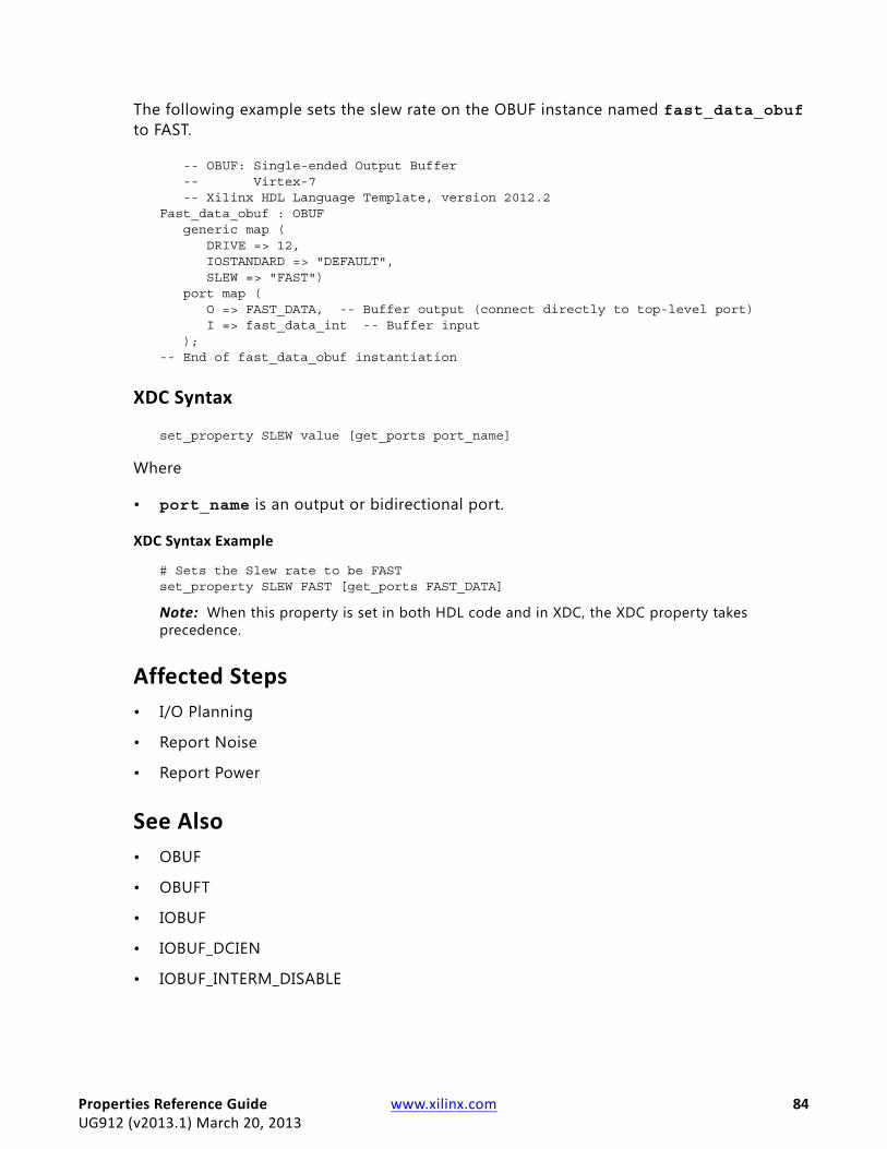
Properties Reference Guide www.xilinx.com 84UG912 (v2013.1) March 20, 2013
The following example sets the slew rate on the OBUF instance named fast_data_obuf to FAST.
-- OBUF: Single-ended Output Buffer -- Virtex-7 -- Xilinx HDL Language Template, version 2012.2Fast_data_obuf : OBUF generic map ( DRIVE => 12, IOSTANDARD => "DEFAULT", SLEW => "FAST") port map ( O => FAST_DATA, -- Buffer output (connect directly to top-level port) I => fast_data_int -- Buffer input );-- End of fast_data_obuf instantiation
XDC Syntax
set_property SLEW value [get_ports port_name]
Where
• port_name is an output or bidirectional port.
XDC Syntax Example
# Sets the Slew rate to be FASTset_property SLEW FAST [get_ports FAST_DATA]
Note: When this property is set in both HDL code and in XDC, the XDC property takes precedence.
Affected Steps• I/O Planning
• Report Noise
• Report Power
See Also• OBUF
• OBUFT
• IOBUF
• IOBUF_DCIEN
• IOBUF_INTERM_DISABLE

Properties Reference Guide www.xilinx.com 85UG912 (v2013.1) March 20, 2013
VCCAUX_IOVCCAUX_IO specif ies the operating voltage of the VCCAUX_IO rail for a given I/O.
DRCs are available to ensure that VCCAUX_IO property assignments are correct:
• VCCAUXIOBT (warning): ensures that ports with VCCAUX_IO values of NORMAL or HIGH are only placed in HP banks.
• VCCAUXIOSTD (warning): ensures that ports with VCCAUX_IO values of NORMAL or HIGH do not use IOSTANDARDs that are only supported in HR banks.
• VCCAUXIO (error): ensures that ports with VCCAUX_IO values of NORMAL are not constrained/placed in the same bank as a port with a VCCAUX_IO value of HIGH.
Architecture SupportAll architectures on High Performance (HP) bank I/O only
Applicable Elements• Ports (get_ports)
• Cells (get_cells)
° I/O buffers
Values• DONTCARE (default)
• NORMAL
• HIGH
Syntax
Verilog Syntax
To set this attribute, place the proper Verilog attribute syntax before the top-level output port declaration.
(* VCCAUXIO = "{DONTCARE|NORMAL|HIGH}" *)
Verilog Syntax Example
// Specifies a “HIGH” voltage for the VCCAUX_IO rail connected to this I/O(* VCCAUX_IO = "HIGH" *) input ACT3,
Properties Reference Guide www.xilinx.com 86UG912 (v2013.1) March 20, 2013
VHDL Syntax
To set this attribute, place the proper VHDL attribute syntax before the top-level output port declaration.
Declare the VHDL attribute as follows:
attribute VCCAUX_IO : string;
Specify the VHDL attribute as follows:
attribute VCCAUX_IO of port_name : signal is value;
Where
• port_name is a top-level port.
VHDL Syntax Example
ACT3 : in std_logic;attribute VCCAUX_IO : string;-- Specifies a “HIGH” voltage for the VCCAUX_IO rail connected to this I/Oattribute VCCAUX_IO of ACT3 : signal is “HIGH”;
XDC Syntax
set_property VCCAUX_IO value [get_ports port_name]
Where
• port_name is a top-level port.
XDC Syntax Example
# Specifies a “HIGH” voltage for the VCCAUX_IO rail connected to this I/Oset_property VCCAUX_IO HIGH [get_ports ACT3]
Note: When this property is set in both HDL code and in XDC, the XDC property takes precedence.
Affected Steps• I/O Planning
• place_design
• Report Power

Properties Reference Guide www.xilinx.com 87UG912 (v2013.1) March 20, 2013
Appendix A
Additional Resources
Xilinx ResourcesFor support resources such as Answers, Documentation, Downloads, and Forums, see the Xilinx® Support website at:
www.xilinx.com/support.
For a glossary of technical terms used in Xilinx documentation, see:
www.xilinx.com/company/terms.htm.
Solution CentersSee the Xilinx Solution Centers for support on devices, software tools, and intellectual property at all stages of the design cycle. Topics include design assistance, advisories, and troubleshooting tips.
References These documents provide supplemental material useful with this guide:
1. Vivado Design Suite 7 Series FPGA Libraries Guide (UG953)
2. 7 Series FPGA Configuration User Guide (UG470)
3. 7 Series FPGAs SelectIO Resources User Guide (UG471)
4. Vivado Design Suite Video Tutorials http://www.xilinx.com/training/vivado/index.htm
5. Vivado Design Suite Documentation www.xilinx.com/support/documentation/dt_vivado2013-1.htm