Embed Size (px)
Citation preview

R
ChipScope Pro 10.1Serial I/O ToolkitUser Guide
UG213 (v10.1) March 24, 2008
ChipScope Pro 10.1 Serial I/O Toolkit www.xilinx.com UG213 (v10.1) March 24, 2008
Xilinx is disclosing this user guide, manual, release note, and/or specification (the "Documentation") to you solely for use in the development of designs to operate with Xilinx hardware devices. You may not reproduce, distribute, republish, download, display, post, or transmit the Documentation in any form or by any means including, but not limited to, electronic, mechanical, photocopying, recording, or otherwise, without the prior written consent of Xilinx. Xilinx expressly disclaims any liability arising out of your use of the Documentation. Xilinx reserves the right, at its sole discretion, to change the Documentation without notice at any time. Xilinx assumes no obligation to correct any errors contained in the Documentation, or to advise you of any corrections or updates. Xilinx expressly disclaims any liability in connection with technical support or assistance that may be provided to you in connection with the Information.
THE DOCUMENTATION IS DISCLOSED TO YOU “AS-IS” WITH NO WARRANTY OF ANY KIND. XILINX MAKES NO OTHER WARRANTIES, WHETHER EXPRESS, IMPLIED, OR STATUTORY, REGARDING THE DOCUMENTATION, INCLUDING ANY WARRANTIES OF MERCHANTABILITY, FITNESS FOR A PARTICULAR PURPOSE, OR NONINFRINGEMENT OF THIRD-PARTY RIGHTS. IN NO EVENT WILL XILINX BE LIABLE FOR ANY CONSEQUENTIAL, INDIRECT, EXEMPLARY, SPECIAL, OR INCIDENTAL DAMAGES, INCLUDING ANY LOSS OF DATA OR LOST PROFITS, ARISING FROM YOUR USE OF THE DOCUMENTATION.
© 2006–2008 Xilinx, Inc. All rights reserved.
XILINX, the Xilinx logo, the Brand Window, and other designated brands included herein are trademarks of Xilinx, Inc. All other trademarks are the property of their respective owners.
Revision History
The following table shows the revision history for this document.
Date Version Revision
02/28/06 1.0 Initial Xilinx release.
09/18/06 8.2 Updated to 8.2i software version.
12/01/06 9.1Updated all chapters to be compatible with 9.1i tools;Updated version number to reflect version number of tools.
01/15/07 9.1.01Updated to include support for Virtex-5RocketIO GTP transceivers;Updated version number to reflect version number of tools.
05/30/07 9.2Updated all chapters to be compatible with 9.2i tools;Updated version number to reflect version number of tools.
03/24/08 10.1
Updated all chapters, including figures and screenshots to be compatible with 10.1 tools;Updated version number to reflect version number of tools.
Added support for Virtex-5 FXT devices. Added Xilinx CORE Generator tool to Table 1-1, page 11. Updated PC and Linux system requirements in Table 1-5, page 18 and Table 1-6, page 18 respectively. Removed Solaris support. Replaced software and licensing sections with updated “Software Installation and Licensing,” page 19. Updated Silicon Revision of Virtex-4 FX Devices, Table 2-1, page 24. Added “Using Multiple Platform Cable USB Connections,” page 44. Added “Sweep Test Settings Panel,” page 68. Added Appendix A, “References.”
R

ChipScope Pro 10.1 Serial I/O Toolkit www.xilinx.com 3UG213 (v10.1) March 24, 2008
Schedule of Figures . . . . . . . . . . . . . . . . . . . . . . . . . . . . . . . . . . . . . . . . . . . . . . . . . . . . . . . . . . 5
Schedule of Tables . . . . . . . . . . . . . . . . . . . . . . . . . . . . . . . . . . . . . . . . . . . . . . . . . . . . . . . . . . . 7
Preface: About This GuideUser Guide Contents . . . . . . . . . . . . . . . . . . . . . . . . . . . . . . . . . . . . . . . . . . . . . . . . . . . . . . . . . 9Additional Support Resources . . . . . . . . . . . . . . . . . . . . . . . . . . . . . . . . . . . . . . . . . . . . . . . . 9TypographicalConventions. . . . . . . . . . . . . . . . . . . . . . . . . . . . . . . . . . . . . . . . . . . . . . . . . . 10
Typographical . . . . . . . . . . . . . . . . . . . . . . . . . . . . . . . . . . . . . . . . . . . . . . . . . . . . . . . . . . . . 10Online Document . . . . . . . . . . . . . . . . . . . . . . . . . . . . . . . . . . . . . . . . . . . . . . . . . . . . . . . . . 10
Chapter 1: IntroductionChipScope Pro Serial I/O Toolkit Overview . . . . . . . . . . . . . . . . . . . . . . . . . . . . . . . . . 11ChipScope Pro Tools Description. . . . . . . . . . . . . . . . . . . . . . . . . . . . . . . . . . . . . . . . . . . . 11
Design Flow . . . . . . . . . . . . . . . . . . . . . . . . . . . . . . . . . . . . . . . . . . . . . . . . . . . . . . . . . . . . . 13ChipScope Pro Serial I/O Toolkit Cores Description . . . . . . . . . . . . . . . . . . . . . . . . . 14
ICON Core . . . . . . . . . . . . . . . . . . . . . . . . . . . . . . . . . . . . . . . . . . . . . . . . . . . . . . . . . . . . . . 14IBERT Core . . . . . . . . . . . . . . . . . . . . . . . . . . . . . . . . . . . . . . . . . . . . . . . . . . . . . . . . . . . . . . 14
System Requirements . . . . . . . . . . . . . . . . . . . . . . . . . . . . . . . . . . . . . . . . . . . . . . . . . . . . . . . 17Software Tools Requirements . . . . . . . . . . . . . . . . . . . . . . . . . . . . . . . . . . . . . . . . . . . . . . 17Communications Requirements . . . . . . . . . . . . . . . . . . . . . . . . . . . . . . . . . . . . . . . . . . . . 17Board Requirements . . . . . . . . . . . . . . . . . . . . . . . . . . . . . . . . . . . . . . . . . . . . . . . . . . . . . . 18Host System Requirements for Microsoft Windows . . . . . . . . . . . . . . . . . . . . . . . . . . . 18Host System Requirements for Linux . . . . . . . . . . . . . . . . . . . . . . . . . . . . . . . . . . . . . . . . 18
Software Installation and Licensing . . . . . . . . . . . . . . . . . . . . . . . . . . . . . . . . . . . . . . . . . 19Related Documents . . . . . . . . . . . . . . . . . . . . . . . . . . . . . . . . . . . . . . . . . . . . . . . . . . . . . . . . . 19
Chapter 2: Using the ChipScope Pro IBERT Core GeneratorIntroduction . . . . . . . . . . . . . . . . . . . . . . . . . . . . . . . . . . . . . . . . . . . . . . . . . . . . . . . . . . . . . . . . 21Core Generator Overview . . . . . . . . . . . . . . . . . . . . . . . . . . . . . . . . . . . . . . . . . . . . . . . . . . . 21Generating an IBERT Core . . . . . . . . . . . . . . . . . . . . . . . . . . . . . . . . . . . . . . . . . . . . . . . . . . 22
General IBERT Options . . . . . . . . . . . . . . . . . . . . . . . . . . . . . . . . . . . . . . . . . . . . . . . . . . . . 23Selecting the IBERT Clocking Options . . . . . . . . . . . . . . . . . . . . . . . . . . . . . . . . . . . . . . . 25Selecting the MGT Options. . . . . . . . . . . . . . . . . . . . . . . . . . . . . . . . . . . . . . . . . . . . . . . . . 28Selecting the General Purpose I/O (GPIO) Options . . . . . . . . . . . . . . . . . . . . . . . . . . . . 31Selecting the Example and Template Options . . . . . . . . . . . . . . . . . . . . . . . . . . . . . . . . . 33Generating the Design . . . . . . . . . . . . . . . . . . . . . . . . . . . . . . . . . . . . . . . . . . . . . . . . . . . . . 34
Chapter 3: Using the ChipScope Pro Core InserterCore Inserter Overview. . . . . . . . . . . . . . . . . . . . . . . . . . . . . . . . . . . . . . . . . . . . . . . . . . . . . . 35
Table of Contents
4 www.xilinx.com ChipScope Pro 10.1 Serial I/O ToolkitUG213 (v10.1) March 24, 2008
R
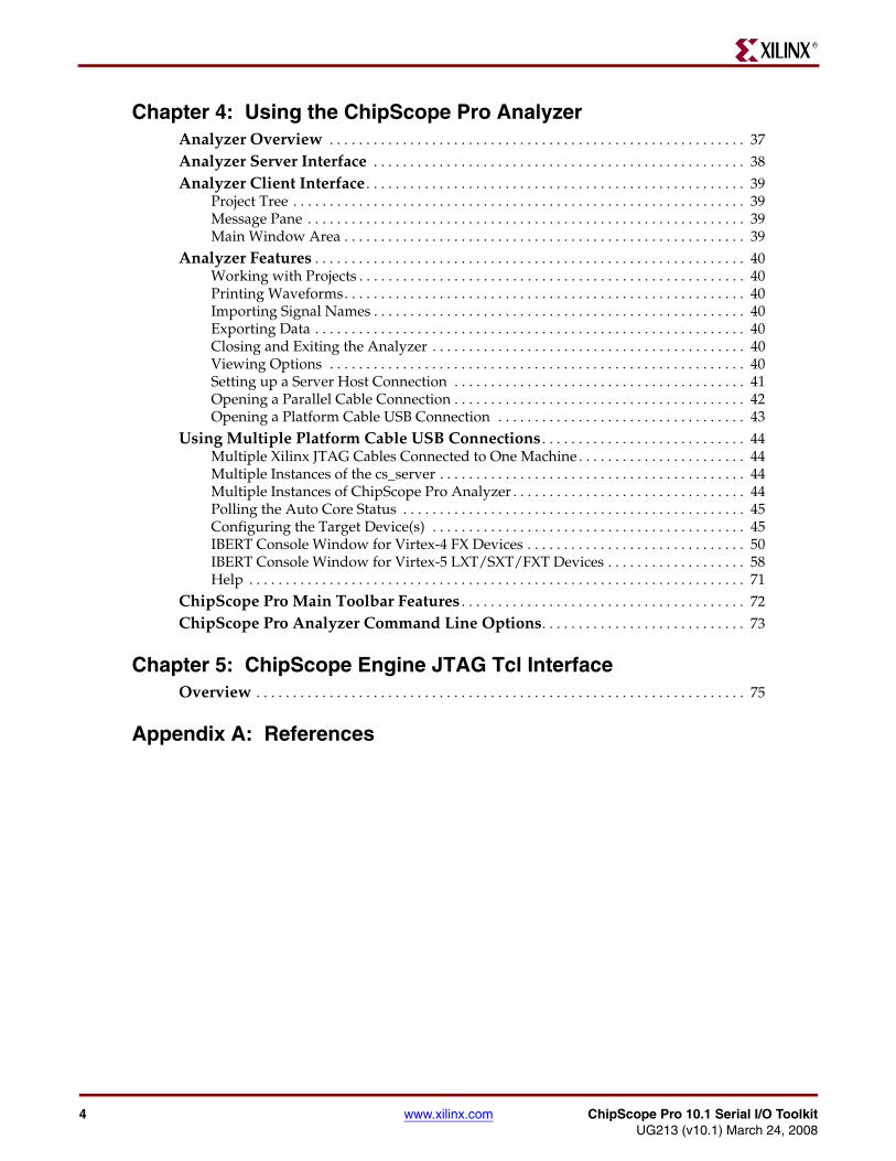
Chapter 4: Using the ChipScope Pro AnalyzerAnalyzer Overview . . . . . . . . . . . . . . . . . . . . . . . . . . . . . . . . . . . . . . . . . . . . . . . . . . . . . . . . . 37Analyzer Server Interface . . . . . . . . . . . . . . . . . . . . . . . . . . . . . . . . . . . . . . . . . . . . . . . . . . . 38Analyzer Client Interface . . . . . . . . . . . . . . . . . . . . . . . . . . . . . . . . . . . . . . . . . . . . . . . . . . . . 39
Project Tree . . . . . . . . . . . . . . . . . . . . . . . . . . . . . . . . . . . . . . . . . . . . . . . . . . . . . . . . . . . . . . 39Message Pane . . . . . . . . . . . . . . . . . . . . . . . . . . . . . . . . . . . . . . . . . . . . . . . . . . . . . . . . . . . . 39Main Window Area . . . . . . . . . . . . . . . . . . . . . . . . . . . . . . . . . . . . . . . . . . . . . . . . . . . . . . . 39
Analyzer Features . . . . . . . . . . . . . . . . . . . . . . . . . . . . . . . . . . . . . . . . . . . . . . . . . . . . . . . . . . . 40Working with Projects . . . . . . . . . . . . . . . . . . . . . . . . . . . . . . . . . . . . . . . . . . . . . . . . . . . . . 40Printing Waveforms. . . . . . . . . . . . . . . . . . . . . . . . . . . . . . . . . . . . . . . . . . . . . . . . . . . . . . . 40Importing Signal Names . . . . . . . . . . . . . . . . . . . . . . . . . . . . . . . . . . . . . . . . . . . . . . . . . . . 40Exporting Data . . . . . . . . . . . . . . . . . . . . . . . . . . . . . . . . . . . . . . . . . . . . . . . . . . . . . . . . . . . 40Closing and Exiting the Analyzer . . . . . . . . . . . . . . . . . . . . . . . . . . . . . . . . . . . . . . . . . . . 40Viewing Options . . . . . . . . . . . . . . . . . . . . . . . . . . . . . . . . . . . . . . . . . . . . . . . . . . . . . . . . . 40Setting up a Server Host Connection . . . . . . . . . . . . . . . . . . . . . . . . . . . . . . . . . . . . . . . . 41Opening a Parallel Cable Connection . . . . . . . . . . . . . . . . . . . . . . . . . . . . . . . . . . . . . . . . 42Opening a Platform Cable USB Connection . . . . . . . . . . . . . . . . . . . . . . . . . . . . . . . . . . 43
Using Multiple Platform Cable USB Connections . . . . . . . . . . . . . . . . . . . . . . . . . . . . 44Multiple Xilinx JTAG Cables Connected to One Machine . . . . . . . . . . . . . . . . . . . . . . . 44Multiple Instances of the cs_server . . . . . . . . . . . . . . . . . . . . . . . . . . . . . . . . . . . . . . . . . . 44Multiple Instances of ChipScope Pro Analyzer . . . . . . . . . . . . . . . . . . . . . . . . . . . . . . . . 44Polling the Auto Core Status . . . . . . . . . . . . . . . . . . . . . . . . . . . . . . . . . . . . . . . . . . . . . . . 45Configuring the Target Device(s) . . . . . . . . . . . . . . . . . . . . . . . . . . . . . . . . . . . . . . . . . . . 45IBERT Console Window for Virtex-4 FX Devices . . . . . . . . . . . . . . . . . . . . . . . . . . . . . . 50IBERT Console Window for Virtex-5 LXT/SXT/FXT Devices . . . . . . . . . . . . . . . . . . . 58Help . . . . . . . . . . . . . . . . . . . . . . . . . . . . . . . . . . . . . . . . . . . . . . . . . . . . . . . . . . . . . . . . . . . . 71
ChipScope Pro Main Toolbar Features . . . . . . . . . . . . . . . . . . . . . . . . . . . . . . . . . . . . . . . 72ChipScope Pro Analyzer Command Line Options. . . . . . . . . . . . . . . . . . . . . . . . . . . . 73
Chapter 5: ChipScope Engine JTAG Tcl InterfaceOverview . . . . . . . . . . . . . . . . . . . . . . . . . . . . . . . . . . . . . . . . . . . . . . . . . . . . . . . . . . . . . . . . . . . 75
Appendix A: References
ChipScope Pro 10.1 Serial I/O Toolkit www.xilinx.com 5UG213 (v10.1) March 24, 2008
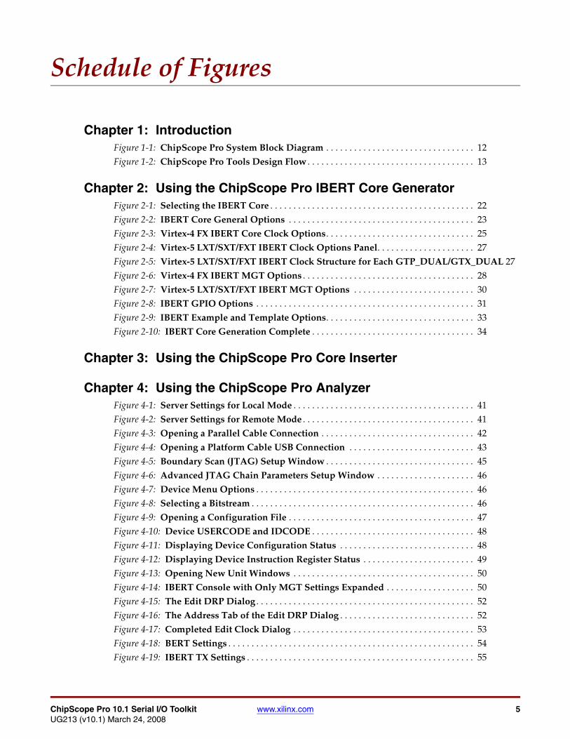
Chapter 1: IntroductionFigure 1-1: ChipScope Pro System Block Diagram . . . . . . . . . . . . . . . . . . . . . . . . . . . . . . . . 12Figure 1-2: ChipScope Pro Tools Design Flow . . . . . . . . . . . . . . . . . . . . . . . . . . . . . . . . . . . . 13
Chapter 2: Using the ChipScope Pro IBERT Core GeneratorFigure 2-1: Selecting the IBERT Core . . . . . . . . . . . . . . . . . . . . . . . . . . . . . . . . . . . . . . . . . . . . 22Figure 2-2: IBERT Core General Options . . . . . . . . . . . . . . . . . . . . . . . . . . . . . . . . . . . . . . . . 23Figure 2-3: Virtex-4 FX IBERT Core Clock Options. . . . . . . . . . . . . . . . . . . . . . . . . . . . . . . . 25Figure 2-4: Virtex-5 LXT/SXT/FXT IBERT Clock Options Panel. . . . . . . . . . . . . . . . . . . . . 27Figure 2-5: Virtex-5 LXT/SXT/FXT IBERT Clock Structure for Each GTP_DUAL/GTX_DUAL 27Figure 2-6: Virtex-4 FX IBERT MGT Options . . . . . . . . . . . . . . . . . . . . . . . . . . . . . . . . . . . . . 28Figure 2-7: Virtex-5 LXT/SXT/FXT IBERT MGT Options . . . . . . . . . . . . . . . . . . . . . . . . . . 30Figure 2-8: IBERT GPIO Options . . . . . . . . . . . . . . . . . . . . . . . . . . . . . . . . . . . . . . . . . . . . . . . 31Figure 2-9: IBERT Example and Template Options. . . . . . . . . . . . . . . . . . . . . . . . . . . . . . . . 33Figure 2-10: IBERT Core Generation Complete . . . . . . . . . . . . . . . . . . . . . . . . . . . . . . . . . . . 34
Chapter 3: Using the ChipScope Pro Core Inserter
Chapter 4: Using the ChipScope Pro AnalyzerFigure 4-1: Server Settings for Local Mode . . . . . . . . . . . . . . . . . . . . . . . . . . . . . . . . . . . . . . . 41Figure 4-2: Server Settings for Remote Mode . . . . . . . . . . . . . . . . . . . . . . . . . . . . . . . . . . . . . 41Figure 4-3: Opening a Parallel Cable Connection . . . . . . . . . . . . . . . . . . . . . . . . . . . . . . . . . 42Figure 4-4: Opening a Platform Cable USB Connection . . . . . . . . . . . . . . . . . . . . . . . . . . . 43Figure 4-5: Boundary Scan (JTAG) Setup Window . . . . . . . . . . . . . . . . . . . . . . . . . . . . . . . . 45Figure 4-6: Advanced JTAG Chain Parameters Setup Window . . . . . . . . . . . . . . . . . . . . . 46Figure 4-7: Device Menu Options . . . . . . . . . . . . . . . . . . . . . . . . . . . . . . . . . . . . . . . . . . . . . . . 46Figure 4-8: Selecting a Bitstream . . . . . . . . . . . . . . . . . . . . . . . . . . . . . . . . . . . . . . . . . . . . . . . . 46Figure 4-9: Opening a Configuration File . . . . . . . . . . . . . . . . . . . . . . . . . . . . . . . . . . . . . . . . 47Figure 4-10: Device USERCODE and IDCODE . . . . . . . . . . . . . . . . . . . . . . . . . . . . . . . . . . . 48Figure 4-11: Displaying Device Configuration Status . . . . . . . . . . . . . . . . . . . . . . . . . . . . . 48Figure 4-12: Displaying Device Instruction Register Status . . . . . . . . . . . . . . . . . . . . . . . . 49Figure 4-13: Opening New Unit Windows . . . . . . . . . . . . . . . . . . . . . . . . . . . . . . . . . . . . . . . 50Figure 4-14: IBERT Console with Only MGT Settings Expanded . . . . . . . . . . . . . . . . . . . 50Figure 4-15: The Edit DRP Dialog . . . . . . . . . . . . . . . . . . . . . . . . . . . . . . . . . . . . . . . . . . . . . . . 52Figure 4-16: The Address Tab of the Edit DRP Dialog . . . . . . . . . . . . . . . . . . . . . . . . . . . . . 52Figure 4-17: Completed Edit Clock Dialog . . . . . . . . . . . . . . . . . . . . . . . . . . . . . . . . . . . . . . . 53Figure 4-18: BERT Settings . . . . . . . . . . . . . . . . . . . . . . . . . . . . . . . . . . . . . . . . . . . . . . . . . . . . . 54Figure 4-19: IBERT TX Settings . . . . . . . . . . . . . . . . . . . . . . . . . . . . . . . . . . . . . . . . . . . . . . . . . 55
Schedule of Figures
6 www.xilinx.com ChipScope Pro 10.1 Serial I/O ToolkitUG213 (v10.1) March 24, 2008
R
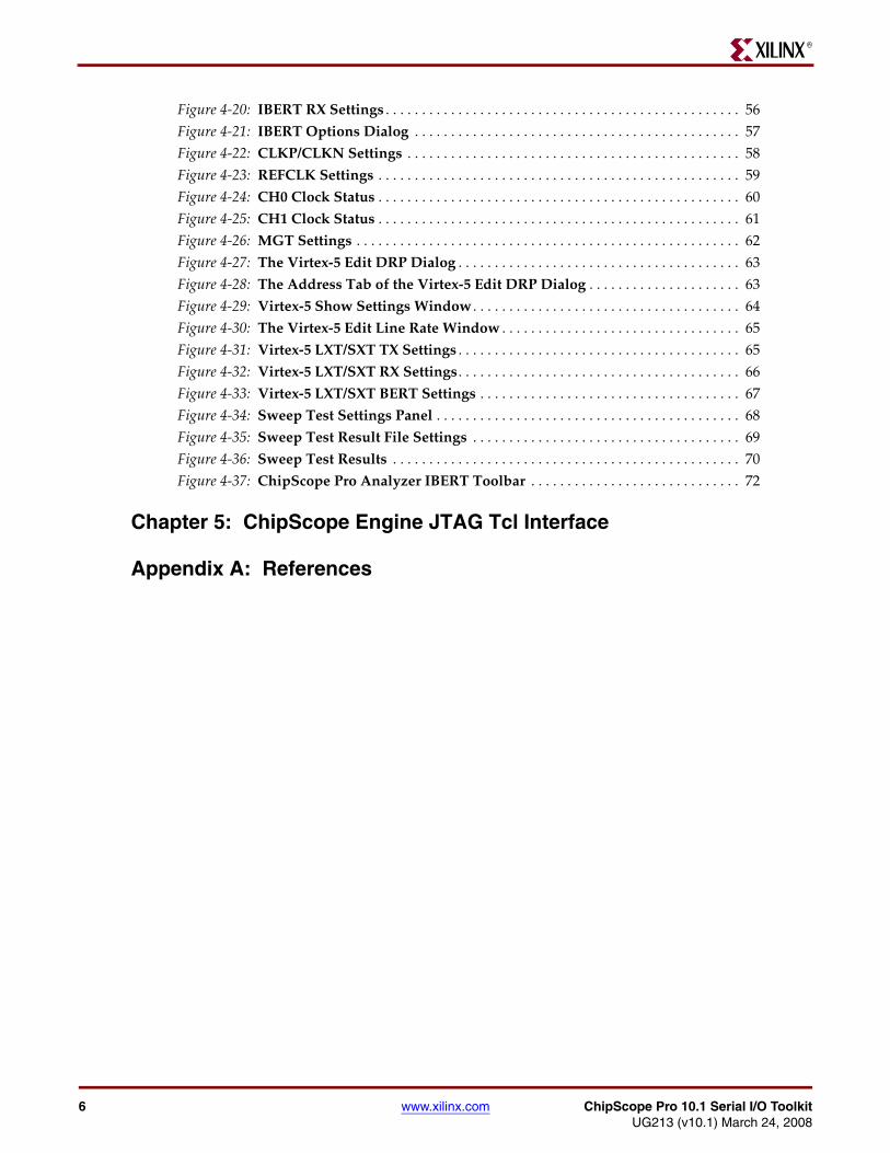
Figure 4-20: IBERT RX Settings . . . . . . . . . . . . . . . . . . . . . . . . . . . . . . . . . . . . . . . . . . . . . . . . . 56Figure 4-21: IBERT Options Dialog . . . . . . . . . . . . . . . . . . . . . . . . . . . . . . . . . . . . . . . . . . . . . 57Figure 4-22: CLKP/CLKN Settings . . . . . . . . . . . . . . . . . . . . . . . . . . . . . . . . . . . . . . . . . . . . . . 58Figure 4-23: REFCLK Settings . . . . . . . . . . . . . . . . . . . . . . . . . . . . . . . . . . . . . . . . . . . . . . . . . . 59Figure 4-24: CH0 Clock Status . . . . . . . . . . . . . . . . . . . . . . . . . . . . . . . . . . . . . . . . . . . . . . . . . . 60Figure 4-25: CH1 Clock Status . . . . . . . . . . . . . . . . . . . . . . . . . . . . . . . . . . . . . . . . . . . . . . . . . . 61Figure 4-26: MGT Settings . . . . . . . . . . . . . . . . . . . . . . . . . . . . . . . . . . . . . . . . . . . . . . . . . . . . . 62Figure 4-27: The Virtex-5 Edit DRP Dialog . . . . . . . . . . . . . . . . . . . . . . . . . . . . . . . . . . . . . . . 63Figure 4-28: The Address Tab of the Virtex-5 Edit DRP Dialog . . . . . . . . . . . . . . . . . . . . . 63Figure 4-29: Virtex-5 Show Settings Window . . . . . . . . . . . . . . . . . . . . . . . . . . . . . . . . . . . . . 64Figure 4-30: The Virtex-5 Edit Line Rate Window . . . . . . . . . . . . . . . . . . . . . . . . . . . . . . . . . 65Figure 4-31: Virtex-5 LXT/SXT TX Settings . . . . . . . . . . . . . . . . . . . . . . . . . . . . . . . . . . . . . . . 65Figure 4-32: Virtex-5 LXT/SXT RX Settings . . . . . . . . . . . . . . . . . . . . . . . . . . . . . . . . . . . . . . . 66Figure 4-33: Virtex-5 LXT/SXT BERT Settings . . . . . . . . . . . . . . . . . . . . . . . . . . . . . . . . . . . . 67Figure 4-34: Sweep Test Settings Panel . . . . . . . . . . . . . . . . . . . . . . . . . . . . . . . . . . . . . . . . . . 68Figure 4-35: Sweep Test Result File Settings . . . . . . . . . . . . . . . . . . . . . . . . . . . . . . . . . . . . . 69Figure 4-36: Sweep Test Results . . . . . . . . . . . . . . . . . . . . . . . . . . . . . . . . . . . . . . . . . . . . . . . . 70Figure 4-37: ChipScope Pro Analyzer IBERT Toolbar . . . . . . . . . . . . . . . . . . . . . . . . . . . . . 72
Chapter 5: ChipScope Engine JTAG Tcl Interface
Appendix A: References
ChipScope Pro 10.1 Serial I/O Toolkit www.xilinx.com 7UG213 (v10.1) March 24, 2008
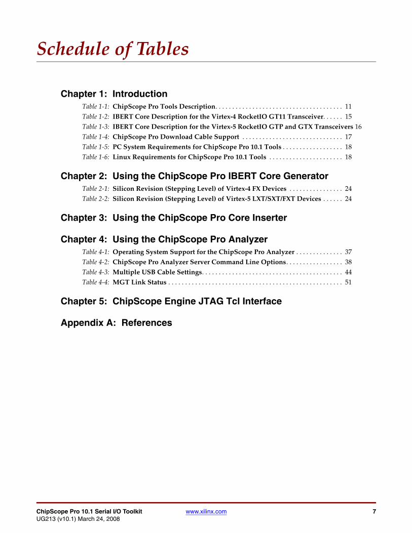
Chapter 1: IntroductionTable 1-1: ChipScope Pro Tools Description. . . . . . . . . . . . . . . . . . . . . . . . . . . . . . . . . . . . . . 11Table 1-2: IBERT Core Description for the Virtex-4 RocketIO GT11 Transceiver. . . . . . 15Table 1-3: IBERT Core Description for the Virtex-5 RocketIO GTP and GTX Transceivers 16Table 1-4: ChipScope Pro Download Cable Support . . . . . . . . . . . . . . . . . . . . . . . . . . . . . . 17Table 1-5: PC System Requirements for ChipScope Pro 10.1 Tools . . . . . . . . . . . . . . . . . . 18Table 1-6: Linux Requirements for ChipScope Pro 10.1 Tools . . . . . . . . . . . . . . . . . . . . . . 18
Chapter 2: Using the ChipScope Pro IBERT Core GeneratorTable 2-1: Silicon Revision (Stepping Level) of Virtex-4 FX Devices . . . . . . . . . . . . . . . . 24Table 2-2: Silicon Revision (Stepping Level) of Virtex-5 LXT/SXT/FXT Devices . . . . . . 24
Chapter 3: Using the ChipScope Pro Core Inserter
Chapter 4: Using the ChipScope Pro AnalyzerTable 4-1: Operating System Support for the ChipScope Pro Analyzer . . . . . . . . . . . . . . 37Table 4-2: ChipScope Pro Analyzer Server Command Line Options. . . . . . . . . . . . . . . . . 38Table 4-3: Multiple USB Cable Settings. . . . . . . . . . . . . . . . . . . . . . . . . . . . . . . . . . . . . . . . . . 44Table 4-4: MGT Link Status . . . . . . . . . . . . . . . . . . . . . . . . . . . . . . . . . . . . . . . . . . . . . . . . . . . . 51
Chapter 5: ChipScope Engine JTAG Tcl Interface
Appendix A: References
Schedule of Tables

8 www.xilinx.com ChipScope Pro 10.1 Serial I/O ToolkitUG213 (v10.1) March 24, 2008
R
ChipScope Pro 10.1 Serial I/O Toolkit www.xilinx.com 9UG213 (v10.1) March 24, 2008
R
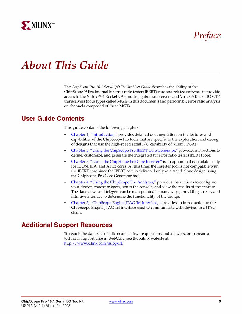
Preface
About This Guide
The ChipScope Pro 10.1 Serial I/O Toolkit User Guide describes the ability of the ChipScope™ Pro internal bit error ratio tester (IBERT) core and related software to provide access to the Virtex™-4 RocketIO™ multi-gigabit transceivers and Virtex-5 RocketIO GTP transceivers (both types called MGTs in this document) and perform bit error ratio analysis on channels composed of these MGTs.
User Guide ContentsThis guide contains the following chapters:
• Chapter 1, “Introduction,” provides detailed documentation on the features and capabilities of the ChipScope Pro tools that are specific to the exploration and debug of designs that use the high-speed serial I/O capability of Xilinx FPGAs.
• Chapter 2, “Using the ChipScope Pro IBERT Core Generator,” provides instructions to define, customize, and generate the integrated bit error ratio tester (IBERT) core.
• Chapter 3, “Using the ChipScope Pro Core Inserter,” is an option that is available only for ICON, ILA, and ATC2 cores. At this time, the Inserter tool is not compatible with the IBERT core since the IBERT core is delivered only as a stand-alone design using the ChipScope Pro Core Generator tool.
• Chapter 4, “Using the ChipScope Pro Analyzer,” provides instructions to configure your device, choose triggers, setup the console, and view the results of the capture. The data views and triggers can be manipulated in many ways, providing an easy and intuitive interface to determine the functionality of the design.
• Chapter 5, “ChipScope Engine JTAG Tcl Interface,” provides an introduction to the ChipScope Engine JTAG Tcl interface used to communicate with devices in a JTAG chain.
Additional Support ResourcesTo search the database of silicon and software questions and answers, or to create a technical support case in WebCase, see the Xilinx website at: http://www.xilinx.com/support.
10 www.xilinx.com ChipScope Pro 10.1 Serial I/O ToolkitUG213 (v10.1) March 24, 2008
Preface: About This GuideR
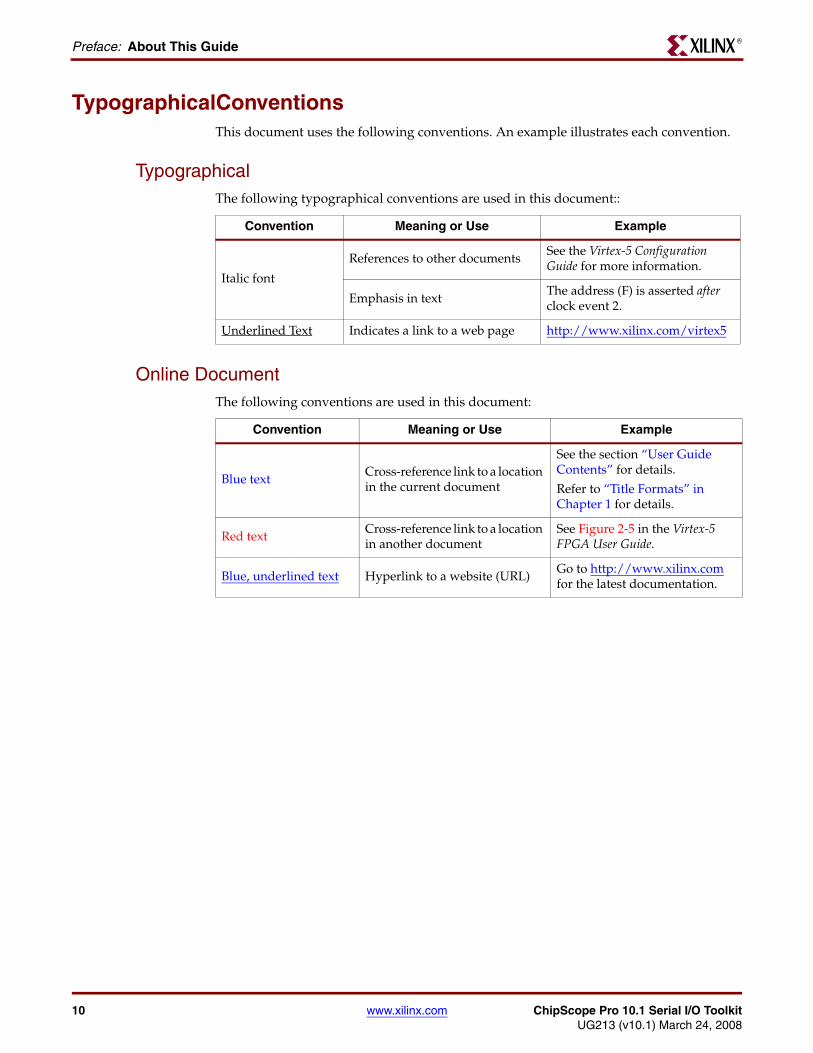
TypographicalConventionsThis document uses the following conventions. An example illustrates each convention.
TypographicalThe following typographical conventions are used in this document::
Online DocumentThe following conventions are used in this document:
Convention Meaning or Use Example
Italic font
References to other documentsSee the Virtex-5 Configuration Guide for more information.
Emphasis in textThe address (F) is asserted after clock event 2.
Underlined Text Indicates a link to a web page http://www.xilinx.com/virtex5
Convention Meaning or Use Example
Blue textCross-reference link to a location in the current document
See the section “User Guide Contents” for details.
Refer to “Title Formats” in Chapter 1 for details.
Red text Cross-reference link to a location in another document
See Figure 2-5 in the Virtex-5 FPGA User Guide.
Blue, underlined text Hyperlink to a website (URL) Go to http://www.xilinx.com for the latest documentation.
ChipScope Pro 10.1 Serial I/O Toolkit www.xilinx.com 11UG213 (v10.1) March 24, 2008
R
Chapter 1
Introduction
ChipScope Pro Serial I/O Toolkit OverviewThe ChipScope Pro 10.1 Serial I/O Toolkit User Guide provides detailed documentation on the features and capabilities of the ChipScope Pro tools that are specific to the exploration and debug of designs that use the high-speed serial I/O capability of Xilinx FPGAs. Specifically, this document describes the ability of the ChipScope Pro internal bit error ratio tester (IBERT) core and related software to provide access to the Virtex-4 RocketIO GT11 transceivers and Virtex-5 RocketIO GTP and GTX transceivers (all three types referred to as MGTs in this document) and perform bit error ratio analysis on channels composed of these MGTs.
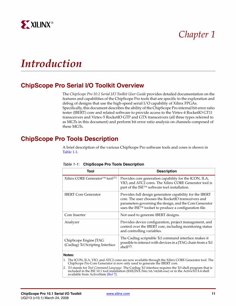
ChipScope Pro Tools DescriptionA brief description of the various ChipScope Pro software tools and cores is shown in Table 1-1.
Table 1-1: ChipScope Pro Tools Description
Tool Description
Xilinx CORE Generator™ tool(1) Provides core generation capability for the ICON, ILA, VIO, and ATC2 cores. The Xilinx CORE Generator tool is part of the ISE™ software tool installation.
IBERT Core Generator Provides full design generation capability for the IBERT core. The user chooses the RocketIO transceivers and parameters governing the design, and the Core Generator uses the ISE™ toolset to produce a configuration file.
Core Inserter Not used to generate IBERT designs.
Analyzer Provides device configuration, project management, and control over the IBERT core, including monitoring status and controlling variables.
ChipScope Engine JTAG (CseJtag) Tcl Scripting Interface
The CseJtag scriptable Tcl command interface makes it possible to interact with devices in a JTAG chain from a Tcl shell(2).
Notes: 1. The ICON, ILA, VIO, and ATC2 cores are now available through the Xilinx CORE Generator tool. The
ChipScope Pro Core Generator is now only used to generate the IBERT core.2. Tcl stands for Tool Command Language. The CseJtag Tcl interface requires the Tcl shell program that is
included in the ISE 10.1 tool installation ($XILINX/bin/nt/xtclsh.exe) or in the ActiveTcl 8.4 shell available from ActiveState [Ref 7].

12 www.xilinx.com ChipScope Pro 10.1 Serial I/O ToolkitUG213 (v10.1) March 24, 2008
Chapter 1: IntroductionR
Figure 1-1 shows a block diagram of a ChipScope Pro system. Users can place the ICON, ILA, IBA/OPB, IBA/PLB, VIO, and ATC2 cores (collectively called the ChipScope Pro cores) into their design by generating the cores with the Core Generator and instantiating them into the HDL source code. You can also insert the ICON, ILA, and ATC2 cores directly into the synthesized design netlist using the Core Inserter tool. The design is then placed and routed using the ISE 10.1 implementation tools. Next, the user downloads the bitstream into the device under test and analyzes the design with the Analyzer software.
The Analyzer tool supports the following download cables for communication between the PC and the devices in the JTAG Boundary Scan chain:
• Platform Cable USB
• Parallel Cable IV
• Parallel Cable III
• MultiPRO (JTAG mode only)
X-Ref Target - Figure 1-1
Figure 1-1: ChipScope Pro System Block Diagram
Board-Under-Test
Host Computer with ChipScope Pro Software
JTAGConnections
cs_pro_sys_blk_diag_ibert
ChipScopePro
Target Device Under Test
ParallelCable
IBERTCore
ICON Core

ChipScope Pro 10.1 Serial I/O Toolkit www.xilinx.com 13UG213 (v10.1) March 24, 2008
ChipScope Pro Tools DescriptionR
Design FlowThe tools design flow (Figure 1-2) merges easily with any standard FPGA design flow that uses a standard HDL synthesis tool and the ISE 10.1 implementation tools.
X-Ref Target - Figure 1-2
Figure 1-2: ChipScope Pro Tools Design Flow
Choose IBERT Options
Generate Design(Calls Xilinx ISE tools)
- Select Bitstream- Modify MGT Parameters- Calculate BER
cs_pro_tools_design_flow_ibert
ChipScope ProCore Generator
14 www.xilinx.com ChipScope Pro 10.1 Serial I/O ToolkitUG213 (v10.1) March 24, 2008
Chapter 1: IntroductionR
ChipScope Pro Serial I/O Toolkit Cores Description
ICON CoreAll of the cores use the JTAG Boundary Scan port to communicate to the host computer via a JTAG download cable. The ICON core provides a communications path between the JTAG Boundary Scan port of the target FPGA and up to 15 ILA, IBA/OPB, IBA/PLB, VIO, and/or ATC2 cores (as shown in Figure 1-1, page 12). For devices other than Virtex-4 or Virtex-5 devices, the ICON core uses either the USER1 or USER2 JTAG Boundary Scan instructions for communication via the BSCAN_VIRTEX primitive. The unused USER1 or USER2 scan chain of the BSCAN_VIRTEX primitive can also be exported for use in your application, if needed.
For Virtex-4 and Virtex-5 devices, the ICON core uses any one of the USER1, USER2, USER3 or USER4 scan chains available via the BSCAN_VIRTEX primitive. In Virtex-4 and Virtex-5 devices, it is not necessary to export unused USER scan chains since each BSCAN_VIRTEX primitive implements a single scan chain.
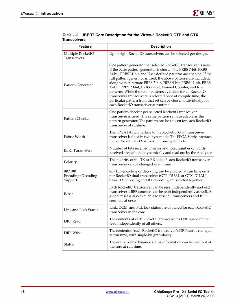
IBERT CoreThe IBERT core has all the logic to control, monitor, and change Virtex-4 and Virtex-5 RocketIO transceiver parameters and perform bit error ratio tests (see Table 1-2, page 15 and Table 1-3, page 16). The IBERT core has three major components:
• BERT Logic
♦ The BERT logic instantiated the actual RocketIO transceiver component, and contains the pattern generators and checkers. A variety of patterns are available, from simple clock-type patterns to full PRBS patterns to framed counter patterns utilizing commas and comma detection.
• Dynamic Reconfiguration Port (DRP) Logic
♦ Each RocketIO transceiver has a Dynamic Reconfiguration Port (DRP) on it, so that transceiver attributes can be changed in system. All attributes and DRP addresses are readable and writable in the IBERT core. Each RocketIO transceiver’s DRP can be accessed individually.
• Control and status logic
♦ Manages the operation of the IBERT core.

ChipScope Pro 10.1 Serial I/O Toolkit www.xilinx.com 15UG213 (v10.1) March 24, 2008
ChipScope Pro Serial I/O Toolkit Cores DescriptionR
Table 1-2: IBERT Core Description for the Virtex-4 RocketIO GT11 Transceiver
Feature Description
Multiple RocketIO Transceivers
Any number of RocketIO transceivers from 1 up to the number of transceivers available in the device can be selected.
Pattern Generator
One pattern generator per selected RocketIO transceiver is used. If the basic pattern generator is chosen, Clk patterns 1/2X, 1/10X, and 1/20X are used with PRBS 7. If the full pattern generator is used, the above patterns are included, along with PRBS 9, 11, 13, 15, 20, 29, and 31. An idle pattern (+K28.5, -K28.5) is available. The pattern can be chosen individually for each RocketIO transceiver at runtime.
Pattern Checker
One pattern checker per selected RocketIO transceiver is used. The same pattern set is available as the pattern generator. The pattern can be chosen individually for each RocketIO transceiver at runtime.
Fabric WidthThe FPGA fabric width to the RocketIO transceiver is customizable on a per-transceiver basis at generate time. Choices are 16, 20, 32, and 40 bits.
BERT ParametersNumber of bits received in error and total number of words received are gathered on the fly and read out by the Analyzer
Polarity The polarity of the TX or RX side of each RocketIO transceiver can be changed at runtime.
8B/10B Encoding/Decoding Support
8B/10B encoding or decoding can be enabled at run time on a per RocketIO transceiver basis. TX encoding and RX decoding can be chosen independently. Only fabric widths of 16 and 32 bits can use 8B/10B encoding.
Reset
Each RocketIO transceiver’s PCS/PMA can be reset independently, and each transceiver’s BER counters can be reset independently as well. A global reset is also available to reset all counters, PCSs, and PMAs at once.
Link and Lock Status
Link status, TX PLL lock status, and RX PLL lock status are gathered for each RocketIO transceiver in the core. An activity bit is also available, indicating if the status bit has changed state since the last time it was read.
DRP ReadThe contents of each RocketIO transceiver’s Dynamic Reconfiguration Port can be read independently of all others.
DRP WriteThe contents of each RocketIO transceiver’s DRP can be changed at run time, with single-bit granularity
StatusThe entire core’s dynamic status information can be read out of the core at run time.
16 www.xilinx.com ChipScope Pro 10.1 Serial I/O ToolkitUG213 (v10.1) March 24, 2008
Chapter 1: IntroductionR
Table 1-3: IBERT Core Description for the Virtex-5 RocketIO GTP and GTX Transceivers
Feature Description
Multiple RocketIO Transceivers
Up to eight RocketIO transceivers can be selected per design.
Pattern Generator
One pattern generator per selected RocketIO transceiver is used. If the basic pattern generator is chosen, the PRBS 7-bit, PRBS 23-bit, PRBS 31-bit, and User-defined patterns are enabled. If the full pattern generator is used, the above patterns are included, along with Alternate PRBS 7-bit, PRBS 9-bit, PRBS 11-bit, PRBS 15-bit, PRBS 20-bit, PRBS 29-bit, Framed Counter, and Idle patterns. While the set of patterns available for all RocketIO transceiver transceivers is selected once at compile time, the particular pattern from that set can be chosen individually for each RocketIO transceiver at runtime.
Pattern Checker
One pattern checker per selected RocketIO transceiver transceiver is used. The same pattern set is available as the pattern generator. The pattern can be chosen for each RocketIO transceiver at runtime.
Fabric WidthThe FPGA fabric interface to the RocketIO GTP transceiver transceiver is fixed in two-byte mode. The FPGA fabric interface to the RocketIO GTX is fixed in four-byte mode.
BERT ParametersNumber of bits received in error and total number of words received are gathered dynamically and read out by the Analyzer.
Polarity The polarity of the TX or RX side of each RocketIO transceiver transceiver can be changed at runtime.
8B/10B Encoding/Decoding Support
8B/10B encoding or decoding can be enabled at run time on a per RocketIO dual-transceiver (GTP_DUAL or GTX_DUAL) basis. TX encoding and RX decoding are selected together.
Reset
Each RocketIO transceiver can be reset independently and each transceiver’s BER counters can be reset independently as well. A global reset is also available to reset all transceivers and BER counters at once.
Link and Lock StatusLink, DCM, and PLL lock status are gathered for each RocketIO transceiver in the core.
DRP ReadThe contents of each RocketIO transceiver’s DRP space can be read independently of all others.
DRP WriteThe contents of each RocketIO transceiver’s DRP can be changed at run time, with single-bit granularity
StatusThe entire core’s dynamic status information can be read out of the core at run time.

ChipScope Pro 10.1 Serial I/O Toolkit www.xilinx.com 17UG213 (v10.1) March 24, 2008
System RequirementsR
System Requirements
Software Tools RequirementsThe Core Inserter, IBERT Core Generator, and Tcl/JTAG tools require that ISE 10.1 implementation tools be installed on your system. (Tcl stands for Tool Command Language and a Tcl shell is a shell program that is used to run Tcl scripts.) Tcl/JTAG requires the Tcl shell that is included in the ISE 10.1 tool installation ($XILINX/bin/nt/xtclsh.exe).
Communications RequirementsThe Analyzer supports the following download cables (see Table 1-4, page 17) for communication between the PC and the devices in the JTAG Boundary Scan chain:
• Platform Cable USB
• Parallel Cable IV
• Parallel Cable III
• MultiPRO
Table 1-4: ChipScope Pro Download Cable Support
Download Cable Features
Platform Cable USB • Uses the USB port (USB 2.0 or USB 1.1) to communicate with the Boundary Scan chain of the board-under-test
• Downloads at speeds up to 24 Mb/s throughput• Contains an adjustable voltage interface that enables it to communicate with systems and
device I/Os operating at 5V down to 1.5V• Windows and Linux OS support
Parallel Cable IV(1) • Uses the parallel port (that is, printer port) to communicate with the Boundary Scan chain of the board-under-test
• Downloads at speeds up to 5 Mb/s throughput• Contains an adjustable voltage interface that enables it to communicate with systems and
device I/Os operating at 5V down to 1.5V• Windows and Linux OS support
Parallel Cable III • Uses the parallel port (that is, printer port) to communicate with the Boundary Scan chain of the board-under-test
• Downloads at speeds up to 500 kb/s throughput• Contains an adjustable voltage interface that enables it to communicate with systems and
device I/Os operating at 5V down to 2.5V• Windows and Linux OS support
MultiPRO Cable • Uses the parallel port (that is, printer port) to communicate with the Boundary Scan chain of the board-under-test
• Downloads at speeds up to 5 Mb/s throughput• Contains an adjustable voltage interface that enables it to communicate with systems and
device I/Os operating at 5V down to 1.5V• Windows OS support only
1. The Parallel Cable IV cable is available for purchase from the Xilinx Online Store (from www.xilinx.com choose Online Store → Programming Cables).

18 www.xilinx.com ChipScope Pro 10.1 Serial I/O ToolkitUG213 (v10.1) March 24, 2008
Chapter 1: IntroductionR
Board RequirementsFor the Analyzer and download cable to work properly with the board-under-test, the following board-level requirements must be met:
• One or more Virtex, Virtex-E Virtex-II, Virtex-II Pro, Virtex-4, Virtex-5, Spartan™-II, Spartan-IIE, Spartan-3, Spartan-3E, Spartan-3A, and Spartan-3A DSP devices (including the QPro™ variants of these families) must be connected to a JTAG header that contains the TDI, TMS, TCK, and TDO pins
• If another device would normally drive the TDI, TMS, or TDI pins of the JTAG chain containing the target device(s), then jumpers on these signals are required to disable these sources, preventing contention with the download cable
• If using the Parallel Cable III download cable, then VCC (2.5V-5.0V) and GND headers must be available for powering the Parallel Cable III cable
• If using the Parallel Cable IV, MultiPRO, or Platform Cable USB download cable, then VREF (1.5-5.0V) and GND headers must be available for connecting to the Parallel Cable IV cable
Host System Requirements for Microsoft WindowsThe Core Generator, Core Inserter, and Analyzer (client and server modes) tools run on PC systems running the Microsoft Windows operating system and meet the requirements outlined in Table 1-5.
Host System Requirements for LinuxThe Core Generator and Core Inserter tools run on workstation systems running the Linux operating system and meet the requirements outlined in Table 1-6.
Note: The Linux version of the 10.1 IBERT Core Generator and Core Inserter tools require ISE 10.1 tools installed on the target system and $XILINX environment variable set up correctly.
Table 1-5: PC System Requirements for ChipScope Pro 10.1 Tools
OS Version Memory Java Environment
Windows XP Professional 32-bit
64-bit1024 MB
Java Run-time Environment version 1.5.0 (automatically included in ChipScope Pro 10.1 software installation)Windows Vista
Business
Table 1-6: Linux Requirements for ChipScope Pro 10.1 Tools
OS Version
Memory Java EnvironmentRed Hat EnterpriseLinux
4 WS32-bit
1024 MBJava Run-time Environment version 1.5.0 (automatically included in ChipScope Pro 10.1 software installation)
5 WS
4 WS64-bit
5 WS

ChipScope Pro 10.1 Serial I/O Toolkit www.xilinx.com 19UG213 (v10.1) March 24, 2008
Software Installation and LicensingR
Software Installation and LicensingFor ChipScope Pro software installation and licensing instructions, refer to the ISE 10.1 Design Suite Release Notes and Installation Guide available in the ISE Documentation [Ref 8].
Related DocumentsThe following documents provide further information:
• UG029, ChipScope Pro 10.1 Software and Cores User Guide [Ref 1]
• UG076, Virtex-4 FPGA RocketIO Multi-Gigabit Transceiver User Guide [Ref 4]
• UG196, Virtex-5 FPGA RocketIO GTP Transceiver User Guide [Ref 5]
• UG198, Virtex-5 FPGA RocketIO GTX Transceiver User Guide [Ref 6]

20 www.xilinx.com ChipScope Pro 10.1 Serial I/O ToolkitUG213 (v10.1) March 24, 2008
Chapter 1: IntroductionR

ChipScope Pro 10.1 Serial I/O Toolkit www.xilinx.com 21UG213 (v10.1) March 24, 2008
R
Chapter 2
Using the ChipScope Pro IBERT Core Generator
IntroductionThis chapter focuses only on generating the Integrated Bit Error Ratio Test (IBERT) core. IBERT core generation differs from all other ChipScope cores in that it generates a full design. The ISE tools take the output of IBERT Core Generator and generate a bitstream file (.bit) rather than a design netlist (.ngc).
Core Generator OverviewThe Xilinx CORE Generator tool is used to generate following Chipscope cores (along with most other Xilinx IP):
• Integrated Controller (ICON)
• Integrated Logic Analyzer (ILA)
• Virtual Input/Output (VIO)
• Agilent Trace Core 2 (ATC2)
For more information on generating and using:
• The ICON, ILA, VIO and ATC2 cores, see
♦ ChipScope Pro 10.1 Software and Cores User Guide [Ref 1]
• The IBA/OPB core in an embedded processor design, see:
♦ ChipScope OPB IBA Data Sheet [Ref 2]
♦ EDK Platform Studio online help [Ref 9]
• The IBA/PLB core in an embedded processor design, see
♦ ChipScope PLB IBA Data Sheet [Ref 3]
♦ EDK Platform Studio online help [Ref 9]

22 www.xilinx.com ChipScope Pro 10.1 Serial I/O ToolkitUG213 (v10.1) March 24, 2008
Chapter 2: Using the ChipScope Pro IBERT Core GeneratorR
Generating an IBERT CoreThe IBERT Core Generator tool provides the ability to define and generate a customized IBERT design. When all of the IBERT parameters have been chosen, a full design is generated, including a bitstream. The IBERT core cannot be included in a user’s design; it can only be generated in its own stand-alone design.
The first screen in the IBERT Core Generator only allows the selection of the IBERT core. Select IBERT (Integrated Bit Error Ratio Tester) core (Figure 2-1), and click Next.
X-Ref Target - Figure 2-1
Figure 2-1: Selecting the IBERT Core
ChipScope Pro 10.1 Serial I/O Toolkit www.xilinx.com 23UG213 (v10.1) March 24, 2008
Generating an IBERT CoreR
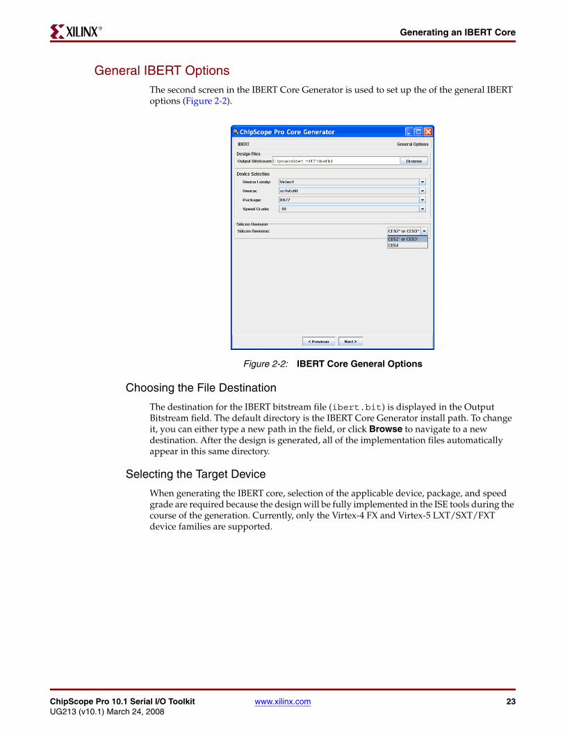
General IBERT OptionsThe second screen in the IBERT Core Generator is used to set up the of the general IBERT options (Figure 2-2).
Choosing the File Destination
The destination for the IBERT bitstream file (ibert.bit) is displayed in the Output Bitstream field. The default directory is the IBERT Core Generator install path. To change it, you can either type a new path in the field, or click Browse to navigate to a new destination. After the design is generated, all of the implementation files automatically appear in this same directory.
Selecting the Target Device
When generating the IBERT core, selection of the applicable device, package, and speed grade are required because the design will be fully implemented in the ISE tools during the course of the generation. Currently, only the Virtex-4 FX and Virtex-5 LXT/SXT/FXT device families are supported.
X-Ref Target - Figure 2-2
Figure 2-2: IBERT Core General Options
24 www.xilinx.com ChipScope Pro 10.1 Serial I/O ToolkitUG213 (v10.1) March 24, 2008
Chapter 2: Using the ChipScope Pro IBERT Core GeneratorR
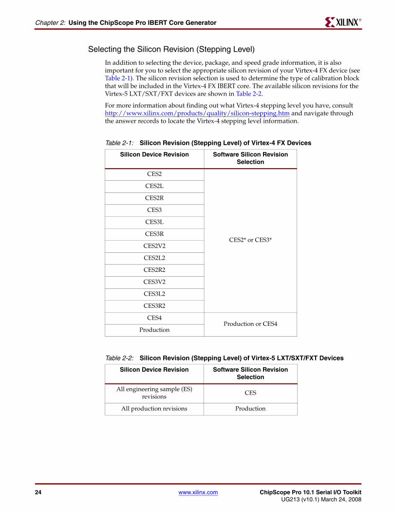
Selecting the Silicon Revision (Stepping Level)
In addition to selecting the device, package, and speed grade information, it is also important for you to select the appropriate silicon revision of your Virtex-4 FX device (see Table 2-1). The silicon revision selection is used to determine the type of calibration block that will be included in the Virtex-4 FX IBERT core. The available silicon revisions for the Virtex-5 LXT/SXT/FXT devices are shown in Table 2-2.
For more information about finding out what Virtex-4 stepping level you have, consult http://www.xilinx.com/products/quality/silicon-stepping.htm and navigate through the answer records to locate the Virtex-4 stepping level information.
Table 2-1: Silicon Revision (Stepping Level) of Virtex-4 FX Devices
Silicon Device Revision Software Silicon Revision Selection
CES2
CES2* or CES3*
CES2L
CES2R
CES3
CES3L
CES3R
CES2V2
CES2L2
CES2R2
CES3V2
CES3L2
CES3R2
CES4Production or CES4
Production
Table 2-2: Silicon Revision (Stepping Level) of Virtex-5 LXT/SXT/FXT Devices
Silicon Device Revision Software Silicon Revision Selection
All engineering sample (ES) revisions
CES
All production revisions Production
ChipScope Pro 10.1 Serial I/O Toolkit www.xilinx.com 25UG213 (v10.1) March 24, 2008
Generating an IBERT CoreR
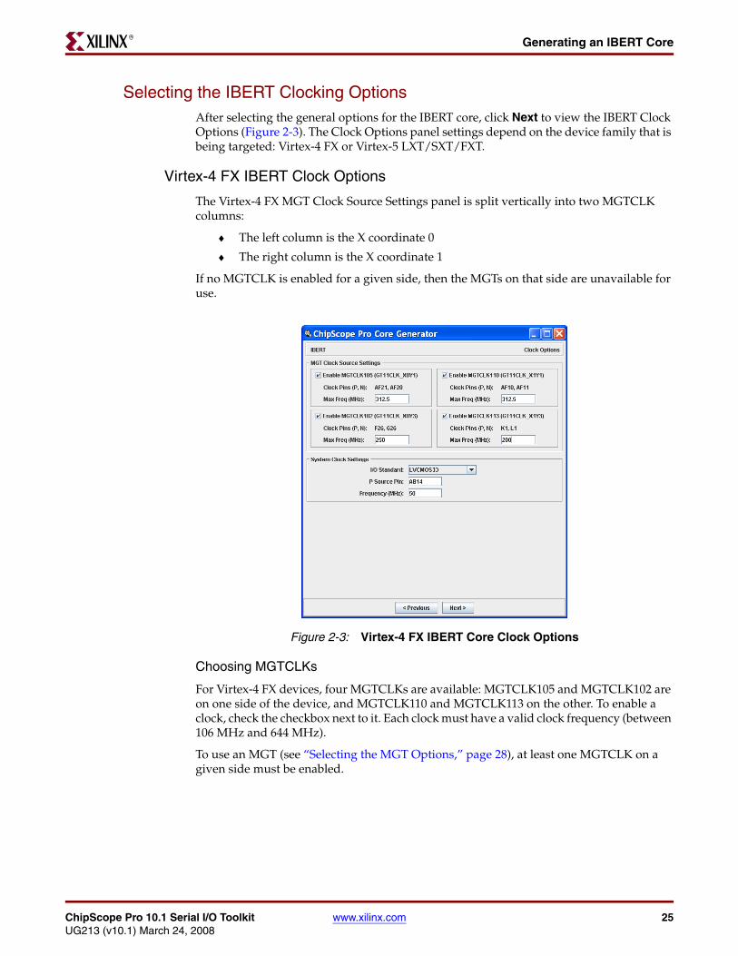
Selecting the IBERT Clocking OptionsAfter selecting the general options for the IBERT core, click Next to view the IBERT Clock Options (Figure 2-3). The Clock Options panel settings depend on the device family that is being targeted: Virtex-4 FX or Virtex-5 LXT/SXT/FXT.
Virtex-4 FX IBERT Clock Options
The Virtex-4 FX MGT Clock Source Settings panel is split vertically into two MGTCLK columns:
♦ The left column is the X coordinate 0
♦ The right column is the X coordinate 1
If no MGTCLK is enabled for a given side, then the MGTs on that side are unavailable for use.
Choosing MGTCLKs
For Virtex-4 FX devices, four MGTCLKs are available: MGTCLK105 and MGTCLK102 are on one side of the device, and MGTCLK110 and MGTCLK113 on the other. To enable a clock, check the checkbox next to it. Each clock must have a valid clock frequency (between 106 MHz and 644 MHz).
To use an MGT (see “Selecting the MGT Options,” page 28), at least one MGTCLK on a given side must be enabled.
X-Ref Target - Figure 2-3
Figure 2-3: Virtex-4 FX IBERT Core Clock Options

26 www.xilinx.com ChipScope Pro 10.1 Serial I/O ToolkitUG213 (v10.1) March 24, 2008
Chapter 2: Using the ChipScope Pro IBERT Core GeneratorR
System Clock Settings
The IBERT core requires a free-running system clock between 32 MHz and 210 MHz. The clock is divided or multiplied internally, resulting in a range of 50 - 100 MHz. To select the clock options:
1. Go to the System Clock Settings section.
2. Specify the I/O Standard from a drop down list of the standards available.
3. Enter the system clock pin location into the P Source Pin text field.
Note: For differential system clock inputs, only type in the P pin location. The ISE implementation tools will automatically determine the N pin location.
4. Enter the system clock frequency in MHz in the Frequency text field.
Note: The system clock frequency must be accurate for the IBERT design to function properly.
ChipScope Pro 10.1 Serial I/O Toolkit www.xilinx.com 27UG213 (v10.1) March 24, 2008
Generating an IBERT CoreR
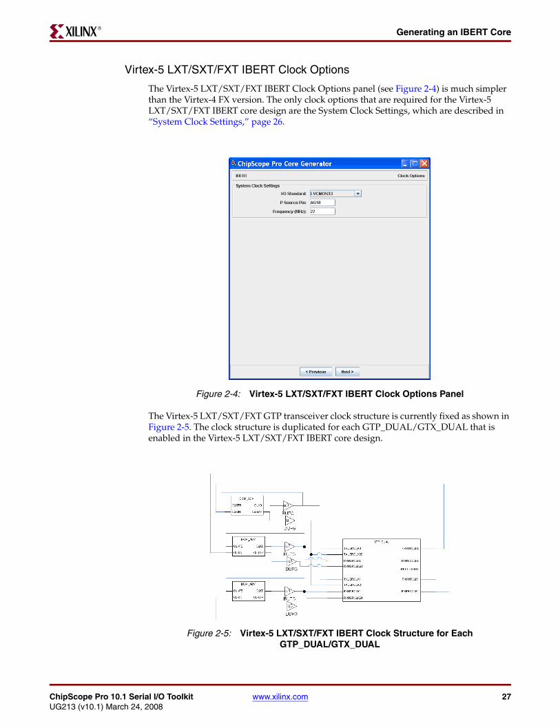
Virtex-5 LXT/SXT/FXT IBERT Clock Options
The Virtex-5 LXT/SXT/FXT IBERT Clock Options panel (see Figure 2-4) is much simpler than the Virtex-4 FX version. The only clock options that are required for the Virtex-5 LXT/SXT/FXT IBERT core design are the System Clock Settings, which are described in “System Clock Settings,” page 26.
The Virtex-5 LXT/SXT/FXT GTP transceiver clock structure is currently fixed as shown in Figure 2-5. The clock structure is duplicated for each GTP_DUAL/GTX_DUAL that is enabled in the Virtex-5 LXT/SXT/FXT IBERT core design.
X-Ref Target - Figure 2-4
Figure 2-4: Virtex-5 LXT/SXT/FXT IBERT Clock Options Panel
X-Ref Target - Figure 2-5
Figure 2-5: Virtex-5 LXT/SXT/FXT IBERT Clock Structure for Each GTP_DUAL/GTX_DUAL

28 www.xilinx.com ChipScope Pro 10.1 Serial I/O ToolkitUG213 (v10.1) March 24, 2008
Chapter 2: Using the ChipScope Pro IBERT Core GeneratorR
Selecting the MGT OptionsAfter selecting the clock options for the IBERT core, click Next to view the IBERT MGT Options (Figure 2-6). The MGT Options panel settings depend on the device family that is being targeted: Virtex-4 FX or Virtex-5 LXT/SXT/FXT.
Virtex-4 FX IBERT MGT Options
The Virtex-4 FX IBERT MGT Options panel is split vertically into two MGT columns (see Figure 2-6):
♦ The left column is the X coordinate 0
♦ The right column is the X coordinate 1
The IBERT core can be configured to include any combination of the MGTs in the device. To enable an MGT, check the checkbox next to the desired MGT. The various information and parameters for that particular MGT will then be enabled (black). If one of the MGTs in a pair is enabled, the other MGT in the pair must be included, even if it is not enabled. If the checkbox next to it is not checked, that MGT will be included in the design as an idle MGT, that is, with no pattern generator or checker logic included.
MGTCLK Source
There are two MGTCLKs for each column of MGTs, and each MGT pair can choose which clock to use for transmitting and receiving data. Both MGTs in an MGT pair must have the same clock settings. This MGTCLK source and multiplier value can be changed at runtime in the ChipScope Pro Analyzer.
X-Ref Target - Figure 2-6
Figure 2-6: Virtex-4 FX IBERT MGT Options

ChipScope Pro 10.1 Serial I/O Toolkit www.xilinx.com 29UG213 (v10.1) March 24, 2008
Generating an IBERT CoreR
Max Line Rate
The line rate of an MGT is a multiple of the frequency of the MGTCLK source, expressed in megabits per second (Mb/s). That multiple is either 8, 10, 16, 20, 32, or 40. For example, if the given MGT chooses MGTCLK102 as its clock source, and MGTCLK102 has a specified frequency of 312.5 MHz, then the line rates in the Max Line Rate combo box is 2500, 3125, 5000, 6250, and 10000.
Max VCO Rate
Some line rates can have multiple Voltage Controlled Oscillator settings. This combo box is populated with the choices available. Many line rates have only one valid VCO setting.
TX User CLK Source
Each active MGT in the IBERT core has logic connected to it that implements the PRBS pattern generators and checkers, as well as other logic. The RX side logic is always clocked by the recovered clock (from the RXRECCLK1 pin of the GT11 component). This recovered clock goes through a global buffer (BUFG) and then to the pattern checker logic. On the TX side, the clock comes from the TXOUTCLK1 pin. However, if the application calls for multiple MGTs to operate at the same clock rate, BUFGs can be conserved by clocking the TX logic of one MGT from a different MGT’s TXOUTCLK1 source. The user can choose which MGT’s TXOUTCLK1 will clock the pattern generator logic. Only MGTs on the same side of the device are available.
Fabric Data Width
Each MGT has a data interface to the FPGA logic, where the pattern generator and checker logic is implemented. This data interface can be 16, 20, 32, or 40 bits wide. Only 16 and 32 bit widths support 8B/10B encoding.
Note: 16 and 20-bit fabric widths are not supported at line rates greater than 6.25 Gb/s.
Pattern Type
The Pattern Type dictates which patterns are available for generating and detecting for a given MGT. If the Basic type is chosen, only CLK1/2X, CLK1/10X, CLK1/20X, and PRBS 7 (X7 + X6 + 1) are available. If the Full type is chosen, all of the Basic patterns are available, in addition to PRBS 9, 11, 15, 20, 23, 29, 31, an alternative PRBS 7 pattern (X7 + X + 1), an Idle pattern, and a Counter pattern. Choosing the Full pattern type makes the design considerably larger, and lengthens generate time.
Resource Usage
The current resource usage of the IBERT core is displayed at the top of the IBERT Options panel. Each time an MGT is checked in the table, an additional MGT is added to the usage. The current number of BUFGs (global clock buffers) is also displayed. The number of BUFGs used cannot exceed 32.

30 www.xilinx.com ChipScope Pro 10.1 Serial I/O ToolkitUG213 (v10.1) March 24, 2008
Chapter 2: Using the ChipScope Pro IBERT Core GeneratorR
Virtex-5 LXT/SXT/FXT IBERT MGT Options
The Virtex-5 LXT/SXT/FXT IBERT MGT Options panel is divided into three sections:
• Resource Usage
• Pattern Settings
• GTP/GTX Settings
Resource Usage
The current resource usage of the IBERT core is displayed at the top of the IBERT Options panel. Each time an GTP_DUAL/GTX_DUAL is checked in the table, an additional GTP_DUAL/GTX_DUAL is added to the total number used. The current number of digital clock managers (DCMs) is also displayed. The number of DCMs used cannot exceed the maximum number of DCMs for the selected FPGA device.
Pattern Settings
The Pattern Type dictates which patterns are available for generation and detection for all GTP_DUAL/GTX_DUALs. The available pattern types are PRBS 7-bit (X7 + X6 + 1), PRBS 7-bit Alt (X7 + X + 1), PRBS 9-bit, PRBS 11-bit, PRBS 15-bit, PRBS 20-bit, PRBS 23-bit, PRBS 29-bit, PRBS 31-bit, User Pattern (which can be used to generate any 20-bit data pattern, including clock patterns), Framed Counter, and Idle Pattern. The default patterns are PRBS 7-bit, PRBS 23-bit, PRBS 31-bit, and User Pattern.
GTP/GTX Settings
In the GTP/GTX Settings section, each GTP_DUAL/GTX_DUAL of the Virtex-5 LXT/SXT/FXT device can be enabled and configured independently from one another. If a GTP_DUAL/GTX_DUAL is enabled, the maximum line rate and appropriate reference clock frequency needs to be specified. Only valid reference clock frequencies, FB, REF, and DIVSEL PLL settings are allowed for a given maximum line rate.
X-Ref Target - Figure 2-7
Figure 2-7: Virtex-5 LXT/SXT/FXT IBERT MGT Options
ChipScope Pro 10.1 Serial I/O Toolkit www.xilinx.com 31UG213 (v10.1) March 24, 2008
Generating an IBERT CoreR
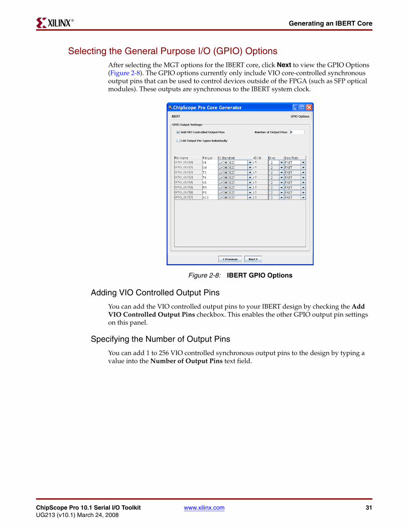
Selecting the General Purpose I/O (GPIO) OptionsAfter selecting the MGT options for the IBERT core, click Next to view the GPIO Options (Figure 2-8). The GPIO options currently only include VIO core-controlled synchronous output pins that can be used to control devices outside of the FPGA (such as SFP optical modules). These outputs are synchronous to the IBERT system clock.
Adding VIO Controlled Output Pins
You can add the VIO controlled output pins to your IBERT design by checking the Add VIO Controlled Output Pins checkbox. This enables the other GPIO output pin settings on this panel.
Specifying the Number of Output Pins
You can add 1 to 256 VIO controlled synchronous output pins to the design by typing a value into the Number of Output Pins text field.
X-Ref Target - Figure 2-8
Figure 2-8: IBERT GPIO Options

32 www.xilinx.com ChipScope Pro 10.1 Serial I/O ToolkitUG213 (v10.1) March 24, 2008
Chapter 2: Using the ChipScope Pro IBERT Core GeneratorR
Editing the Output Pin Parameters
You need to specify the location and other characteristics of the GPIO output pins in the Core Generator. Using the Edit Output Pin Types Individually checkbox, you can control the location, I/O standard, output drive and slew rate of each individual GPIO_OUT pin. Leaving the Edit Output Pin Types Individually checkbox empty allows you to specify the IO Standard, VCCO, Drive and Slew Rate as a group of pins.
Pin Name
The IBERT core currently only supports GPIO output pins that are called GPIO_OUT[n] (where n is the bit index into the bus called GPIO_OUT). The names of the pins cannot be changed.
Pin Loc
The Pin Loc column is used to set the location of the GPIO_OUT pin.
IO Standard
The IO Standard column is used to set the I/O standard of each individual GPIO_OUT pin. The IO standards that are available for selection depend on the device family. Currently, only single-ended IO standards are supported by the IBERT GPIO output pin feature. The names of the IO standards are the same as those in the IOSTANDARD section of the Constraints Guide in the Xilinx Software Manual at http://www.xilinx.com/support.
VCCO
The VCCO column setting denotes the output voltage of the pin driver and depends on the IO Standard selection.
Drive
The Drive column setting denotes the maximum output drive current of the pin driver and ranges from 2 to 24 mA, depending on the IO Standard selection.
Slew Rate
The Slew Rate column can be set to either FAST or SLOW for each individual GPIO_OUT pin.
ChipScope Pro 10.1 Serial I/O Toolkit www.xilinx.com 33UG213 (v10.1) March 24, 2008
Generating an IBERT CoreR
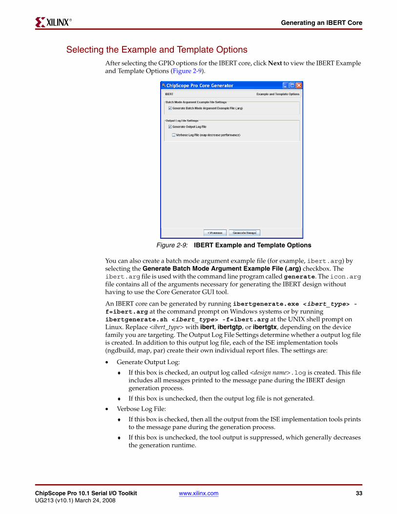
Selecting the Example and Template OptionsAfter selecting the GPIO options for the IBERT core, click Next to view the IBERT Example and Template Options (Figure 2-9).
You can also create a batch mode argument example file (for example, ibert.arg) by selecting the Generate Batch Mode Argument Example File (.arg) checkbox. The ibert.arg file is used with the command line program called generate. The icon.arg file contains all of the arguments necessary for generating the IBERT design without having to use the Core Generator GUI tool.
An IBERT core can be generated by running ibertgenerate.exe <ibert_type> -f=ibert.arg at the command prompt on Windows systems or by running ibertgenerate.sh <ibert_type> -f=ibert.arg at the UNIX shell prompt on Linux. Replace <ibert_type> with ibert, ibertgtp, or ibertgtx, depending on the device family you are targeting. The Output Log File Settings determine whether a output log file is created. In addition to this output log file, each of the ISE implementation tools (ngdbuild, map, par) create their own individual report files. The settings are:
• Generate Output Log:
♦ If this box is checked, an output log called <design name>.log is created. This file includes all messages printed to the message pane during the IBERT design generation process.
♦ If this box is unchecked, then the output log file is not generated.
• Verbose Log File:
♦ If this box is checked, then all the output from the ISE implementation tools prints to the message pane during the generation process.
♦ If this box is unchecked, the tool output is suppressed, which generally decreases the generation runtime.
X-Ref Target - Figure 2-9
Figure 2-9: IBERT Example and Template Options
34 www.xilinx.com ChipScope Pro 10.1 Serial I/O ToolkitUG213 (v10.1) March 24, 2008
Chapter 2: Using the ChipScope Pro IBERT Core GeneratorR
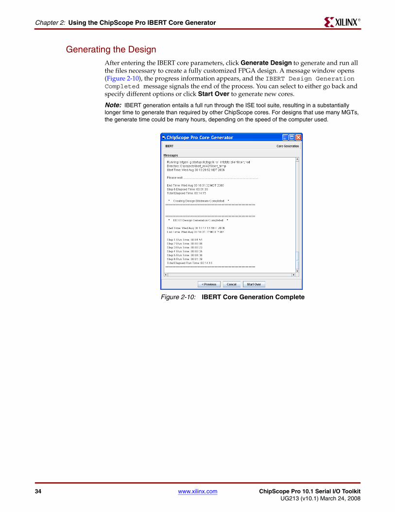
Generating the DesignAfter entering the IBERT core parameters, click Generate Design to generate and run all the files necessary to create a fully customized FPGA design. A message window opens (Figure 2-10), the progress information appears, and the IBERT Design Generation Completed message signals the end of the process. You can select to either go back and specify different options or click Start Over to generate new cores.
Note: IBERT generation entails a full run through the ISE tool suite, resulting in a substantially longer time to generate than required by other ChipScope cores. For designs that use many MGTs, the generate time could be many hours, depending on the speed of the computer used.
X-Ref Target - Figure 2-10
Figure 2-10: IBERT Core Generation Complete
ChipScope Pro 10.1 Serial I/O Toolkit www.xilinx.com 35UG213 (v10.1) March 24, 2008
R
Chapter 3
Using the ChipScope Pro Core Inserter
Core Inserter OverviewThe ChipScope Pro Core Inserter is a post-synthesis tool used to generate a netlist that includes the user design as well as parameterized ICON, ILA, and ATC2 cores as needed. The Core Inserter cannot be used to insert IBERT cores into the user design because the IBERT core is currently delivered as a stand-alone design only. For more information on how to use the Inserter tool to insert ICON, ILA, and ATC2 cores into your design, see the ChipScope Pro 10.1 Software and Cores User Guide [Ref 1].

36 www.xilinx.com ChipScope Pro 10.1 Serial I/O ToolkitUG213 (v10.1) March 24, 2008
Chapter 3: Using the ChipScope Pro Core InserterR

ChipScope Pro 10.1 Serial I/O Toolkit www.xilinx.com 37UG213 (v10.1) March 24, 2008
R
Chapter 4
Using the ChipScope Pro Analyzer
Analyzer OverviewThe ChipScope Pro Analyzer tool interfaces directly to the ICON, ILA, IBA/OPB, IBA/PLB, VIO, ATC2, and IBERT cores (collectively called the ChipScope Pro cores). You can configure your device, choose triggers, setup the console, and view the results of the capture. The data views and triggers can be manipulated in many ways, providing an easy and intuitive interface to determine the functionality of the design.
Note: Even though the Analyzer tool will detect the presence of an ATC2 core, an Agilent Logic Analyzer attached to a JTAG cable is required to control and communicate with the ATC2 core.
The Analyzer tool is made up of two distinct applications: the server and the client. The Analyzer server is a command line application that connects to the JTAG chain of the target system using any of the supported JTAG download cables shown in Table 4-1. The Analyzer client is a graphical user interface (GUI) application that allows you to interact with the devices in the JTAG chain and the cores that are found in those devices.
The Analyzer server and client can run on the same machine (local host mode) or on different machines (remote mode). Remote mode is useful in the following situations:
• You need to debug a system that is in a different location
• You need to share a single system resource with other team members
• You need to demonstrate a problem or feature to someone who is not at your location
Remote mode is available on all operating systems, as shown in Table 4-1.
Table 4-1: Operating System Support for the ChipScope Pro Analyzer
ApplicationWindows XP Pro(32-bit and 64-bit)
Red Hat Linux EnterprisesWS 3 and 4
(32-bit and 64-bit)
Analyzer Server
Yes
Supported JTAG cables:
• Platform Cable USB• Parallel Cable IV• Parallel Cable III• MultiPRO
Yes
Supported JTAG cables:
• Platform Cable USB• Parallel Cable IV• Parallel Cable III• MultiPRO
Analyzer Client
Yes
(Local and Remote)
Yes
(Local and Remote)

38 www.xilinx.com ChipScope Pro 10.1 Serial I/O ToolkitUG213 (v10.1) March 24, 2008
Chapter 4: Using the ChipScope Pro AnalyzerR
Analyzer Server InterfaceThe Analyzer server command line application is available on Windows and Linux operating systems, as shown in Table 4-1, page 37. If you desire to debug a target system that is connected directly to your local machine via a JTAG download cable, then you do not need to start the server manually. You only need to start the server application manually when you desire to interact with the server from a remote client.
Note: The Analyzer server application can handle only one client connection at a time.
The server can be started as follows:
• The Analyzer server is started on Windows machines by executing $CHIPSCOPE/cs_server.bat <command line options>
• The Analyzer server is started on Linux machines by executing $CHIPSCOPE/bin/lin/cs_server.sh <command line options>
where the $CHIPSCOPE environment variable points to the 10.1 installation directory. The Analyzer server application has several <command line options> that are described in Table 4-2. You can customize the server scripts as needed.
Refer to “Setting up a Server Host Connection,” page 41 for more information on how to connect to the server application from the Analyzer client application.
Table 4-2: ChipScope Pro Analyzer Server Command Line Options
Command Line Option Description
-port <portnumber> Used to specify the TCP/IP port number that is used by the client and server to establish a connection. The default port number is 50001.
-password <password> Used to protect the server from unauthorized access. No password is set by default.
-l <logfile> Used to specify the location of the log file. The default log file location is:
$HOME/.chipscope/cs_analyzer_<portnumber>.log
where $HOME is the users home directory and <portnumber> is the TCP/IP port number used by the server.

ChipScope Pro 10.1 Serial I/O Toolkit www.xilinx.com 39UG213 (v10.1) March 24, 2008
Analyzer Client InterfaceR
Analyzer Client InterfaceThe Analyzer client interface consists of four parts:
• Project tree in the upper part of the split pane on the left side of the window
• Signal browser in the lower part of the split pane on the left side of the window
• Message pane at the bottom of the window
• Main window area
Both the project tree/signal browser split pane and the Message pane can be hidden by deselecting those options in the View menu. Additionally, the size of each pane can be adjusted by dragging the bar located between the panes to a new location. Each pane can be maximized or minimized by clicking on the arrow buttons on the pane separator bars. This chapter focuses on the interface to the IBERT core. Some parts of the ChipScope Analyzer (like the Signal Browser) are not used with the IBERT core, and are not addressed in this chapter. For information on those features, see the ChipScope Pro 10.1 Software and Cores User Guide [Ref 1].
Project TreeThe project tree is a graphical representation of the JTAG chain and the cores in the devices in the chain. Although all devices in the chain are displayed in the tree, only valid target devices (Virtex, Virtex-E, Virtex-II, Virtex-II Pro, Virtex-4, Virtex-5, Spartan-II, Spartan-IIE, Spartan-3, Spartan-3E, Spartan-3A, Spartan-3A DSP, and their QPro variants) can contain cores and be operated upon. Leaf nodes in the tree appear when further operations are available.
For instance, a leaf node for each unit appears when that device is configured with a core-enabled bitstream. Context-sensitive menus are available for each level of hierarchy in the tree. To access the context-sensitive menu, right-click on the node in the tree. Device and unit renaming, child window opening, device configuration, and project operations can all be done through these menus. To rename a device or core unit node in the project tree, right-click on the node and select Rename. To end the editing, press Enter or the up or down arrow key, or click on another node in the tree.
Message PaneThe Message pane displays a scroll list of status messages. Error messages appear in red. The Message pane can be resized by dragging the split bar above it to a new location. This also changes the height of the project tree/signal browser split pane.
Main Window AreaThe main window area can display multiple child windows (such as Trigger, Waveform, Listing, Plot windows) at the same time. Each window can be resized, minimized, maximized, and moved as needed.

40 www.xilinx.com ChipScope Pro 10.1 Serial I/O ToolkitUG213 (v10.1) March 24, 2008
Chapter 4: Using the ChipScope Pro AnalyzerR
Analyzer Features
Working with ProjectsProjects hold important information about the Analyzer program state, such as signal naming, signal ordering, bus configurations, and trigger conditions. They allow you to conveniently store and retrieve this information between Analyzer sessions
When you first run the Analyzer tool, a new project is automatically created and is titled new project. To open an existing project, select File → Open Project, or select one of the recently used projects in the File menu. The title bar of the Analyzer and the project tree displays the project name. If the new project is not saved during the course of the session, a dialog box appears when the Analyzer is about to exit, asking you if you wish to save the project.
Creating and Saving A New Project
To create a new project, select File → New Project. A new project called new project is created and made active in the Analyzer. To save the new project under a different name, select File → Save Project. The project file will have a .cpj extension.
Saving Projects
To rename the current project, or to save a copy to another filename, select File → Save Project As, type the new name in the File name dialog box, and click Save.
Printing WaveformsThe IBERT core does not have waveforms, therefore, this menu option is not applicable.
Importing Signal NamesThe IBERT core does not have signals connected to it the way ILA, IBA/PLB, IBA/OPB, and VIO, so the File → Import menu option is not applicable.
Exporting DataThe IBERT core does not capture data to export, so this menu option is not applicable.
Closing and Exiting the AnalyzerTo exit the Analyzer, select File → Exit. The current active project is automatically saved upon exit.
Viewing OptionsThe split pane on the left of the Analyzer window and the Message pane at the bottom of the window can both be hidden or displayed per the user’s choice. Both are displayed the first time the Analyzer is launched. To hide the project tree/signal browser split pane, uncheck it under View → Project Tree. To hide the Message pane, uncheck it under View → Messages.
ChipScope Pro 10.1 Serial I/O Toolkit www.xilinx.com 41UG213 (v10.1) March 24, 2008
Analyzer FeaturesR
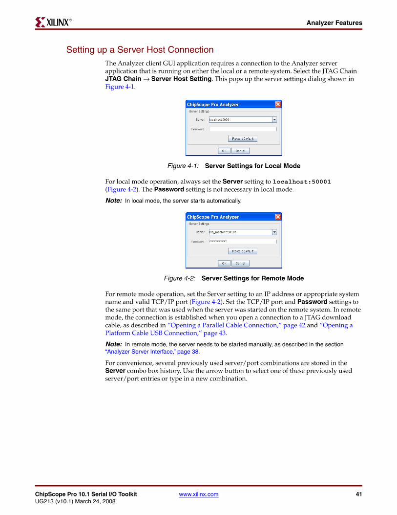
Setting up a Server Host ConnectionThe Analyzer client GUI application requires a connection to the Analyzer server application that is running on either the local or a remote system. Select the JTAG Chain JTAG Chain → Server Host Setting. This pops up the server settings dialog shown in Figure 4-1.
For local mode operation, always set the Server setting to localhost:50001 (Figure 4-2). The Password setting is not necessary in local mode.
Note: In local mode, the server starts automatically.
For remote mode operation, set the Server setting to an IP address or appropriate system name and valid TCP/IP port (Figure 4-2). Set the TCP/IP port and Password settings to the same port that was used when the server was started on the remote system. In remote mode, the connection is established when you open a connection to a JTAG download cable, as described in “Opening a Parallel Cable Connection,” page 42 and “Opening a Platform Cable USB Connection,” page 43.
Note: In remote mode, the server needs to be started manually, as described in the section “Analyzer Server Interface,” page 38.
For convenience, several previously used server/port combinations are stored in the Server combo box history. Use the arrow button to select one of these previously used server/port entries or type in a new combination.
X-Ref Target - Figure 4-1
Figure 4-1: Server Settings for Local Mode
X-Ref Target - Figure 4-2
Figure 4-2: Server Settings for Remote Mode
42 www.xilinx.com ChipScope Pro 10.1 Serial I/O ToolkitUG213 (v10.1) March 24, 2008
Chapter 4: Using the ChipScope Pro AnalyzerR
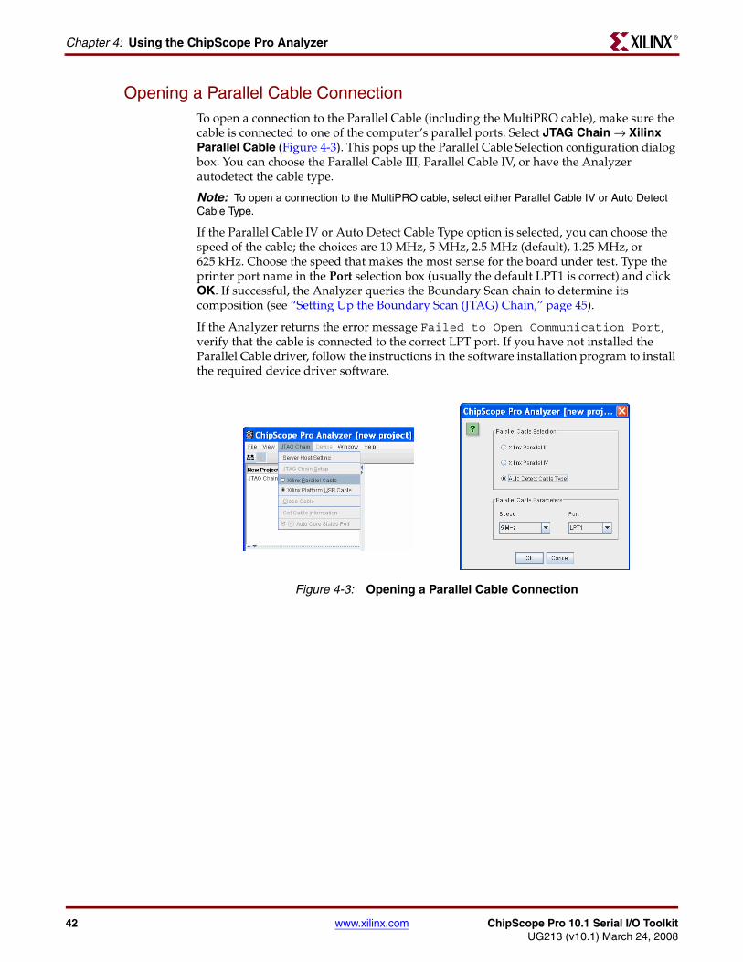
Opening a Parallel Cable ConnectionTo open a connection to the Parallel Cable (including the MultiPRO cable), make sure the cable is connected to one of the computer’s parallel ports. Select JTAG Chain → Xilinx Parallel Cable (Figure 4-3). This pops up the Parallel Cable Selection configuration dialog box. You can choose the Parallel Cable III, Parallel Cable IV, or have the Analyzer autodetect the cable type.
Note: To open a connection to the MultiPRO cable, select either Parallel Cable IV or Auto Detect Cable Type.
If the Parallel Cable IV or Auto Detect Cable Type option is selected, you can choose the speed of the cable; the choices are 10 MHz, 5 MHz, 2.5 MHz (default), 1.25 MHz, or 625 kHz. Choose the speed that makes the most sense for the board under test. Type the printer port name in the Port selection box (usually the default LPT1 is correct) and click OK. If successful, the Analyzer queries the Boundary Scan chain to determine its composition (see “Setting Up the Boundary Scan (JTAG) Chain,” page 45).
If the Analyzer returns the error message Failed to Open Communication Port, verify that the cable is connected to the correct LPT port. If you have not installed the Parallel Cable driver, follow the instructions in the software installation program to install the required device driver software.
X-Ref Target - Figure 4-3
Figure 4-3: Opening a Parallel Cable Connection

ChipScope Pro 10.1 Serial I/O Toolkit www.xilinx.com 43UG213 (v10.1) March 24, 2008
Analyzer FeaturesR
Opening a Platform Cable USB ConnectionTo open a connection to the Platform cable (including the MultiPRO cable), make sure the cable is connected to one of the computer’s parallel ports. Selecting the JTAG Chain → Xilinx Platform USB Cable menu option pops up a dialog window (Figure 4-4).
Platform Cable USB Clock Speeds
You can choose the speed of the cable from any of the settings: 24 MHz, 12 MHz, 6 MHz, 3 MHz (default), 1.5 MHz, or 750 kHz. Choose the speed that makes the most sense for the board under test.
Platform Cable USB Port Number
You can also choose the USB port from a selection of port enumerations in the range of USB2<n>, where <n> is an integer value is 1 through 127. The default port setting is USB21. The USB port enumeration number is based on the order in which the Platform Cable USB download cables are plugged into USB ports of the system. For instance, the first Platform Cable USB download cable plugged into the system is assigned the port enumeration of USB21, the second cable is assigned USB22, and so on.
Note: The enumerations are not necessarily preserved when the system is power cycled. Also, there is currently no way to identify a particular Platform Cable USB other than by physically plugging the cables into the system in a particular order.
X-Ref Target - Figure 4-4
Figure 4-4: Opening a Platform Cable USB Connection

44 www.xilinx.com ChipScope Pro 10.1 Serial I/O ToolkitUG213 (v10.1) March 24, 2008
Chapter 4: Using the ChipScope Pro AnalyzerR
Using Multiple Platform Cable USB ConnectionsTo use ChipScope Pro Analyzer with multiple cables, you need three things:
1. “Multiple Xilinx JTAG Cables Connected to One Machine”
2. “Multiple Instances of the cs_server” application running on one machine, each one listening to a different port
3. “Multiple Instances of ChipScope Pro Analyzer” running on that same machine, or a different machine (via the remote server feature)
Multiple Xilinx JTAG Cables Connected to One MachineTo interact with multiple JTAG cables connected to the same machine, you first need to be able to connect multiple Platform Cable USB, Parallel Cable III, or Parallel Cable IV cables to the machine. In the case of Platform Cable USB cables, you may need to use one or more USB hubs depending on how many cables you need. In the case of PC3/PC4, you may need one or more parallel port extender cards.
Note: Currently, enumerations are not associated with a particular physical Platform Cable USB cable. This means that rebooting your machine may result in different associations between enumerations and physical cables. One work-around is to unplug all cables and re-plug them in the order you wish for them to be enumerated.
Multiple Instances of the cs_serverSet up the ChipScope Pro Analyzer to use multiple cables first by starting multiple instances of the cs_server.exe Windows application or cs_server.sh Linux application on the same machine using different ports. For instance, to start up two servers on different ports on Linux, use:
# cs_server.sh -port 50001
# cs_server.sh -port 50002
Multiple Instances of ChipScope Pro AnalyzerStart and configure multiple ChipScope Pro Analyzer client instances as shown in Table 4-3. Each instance of the Analyzer will connect to a different cs_server and cable enumeration.
Table 4-3: Multiple USB Cable Settings
Analyzer Instance #
Server Host SettingPlatform Cable
USB Port #
1 <IP Address>:50001 USB21
2 <IP Address>:50002 USB22
ChipScope Pro 10.1 Serial I/O Toolkit www.xilinx.com 45UG213 (v10.1) March 24, 2008
Using Multiple Platform Cable USB ConnectionsR
Polling the Auto Core StatusWhen cores are armed, the interface cable queries the cores on a regular basis to determine the status of the capture. If other programs are using the cable at the same time as the Analyzer, it can be beneficial to turn this polling off. This can be done in the JTAG Chain menu by unchecking JTAG Chain → Auto Core Status Poll.
If this polling option is unchecked, when the Run or Trigger Immediate operation is performed, the Analyzer will not query the cores automatically to determine the status. This does not completely disable communication with the cable; it only disables the periodic polling when cores are armed. If one or more cores trigger after the polling has been turned off, the capture buffer will not be downloaded from the device and displayed in any of the data viewer(s) until the Auto Core Status Poll option is turned on again.
Configuring the Target Device(s)You can use the Analyzer software with one or more valid target devices. The first step is to set up all of the devices in the Boundary Scan chain.
Setting Up the Boundary Scan (JTAG) Chain
After the Analyzer has successfully communicated with a download cable, it automatically queries the Boundary Scan (JTAG) chain to find its composition. All Xilinx FPGA, CPLD, PROM, and System ACE devices are automatically detected. The entire IDCODE can be verified for valid target devices. To view the chain composition, select JTAG Chain → JTAG Chain Setup. A dialog box appears with all detected devices in order.
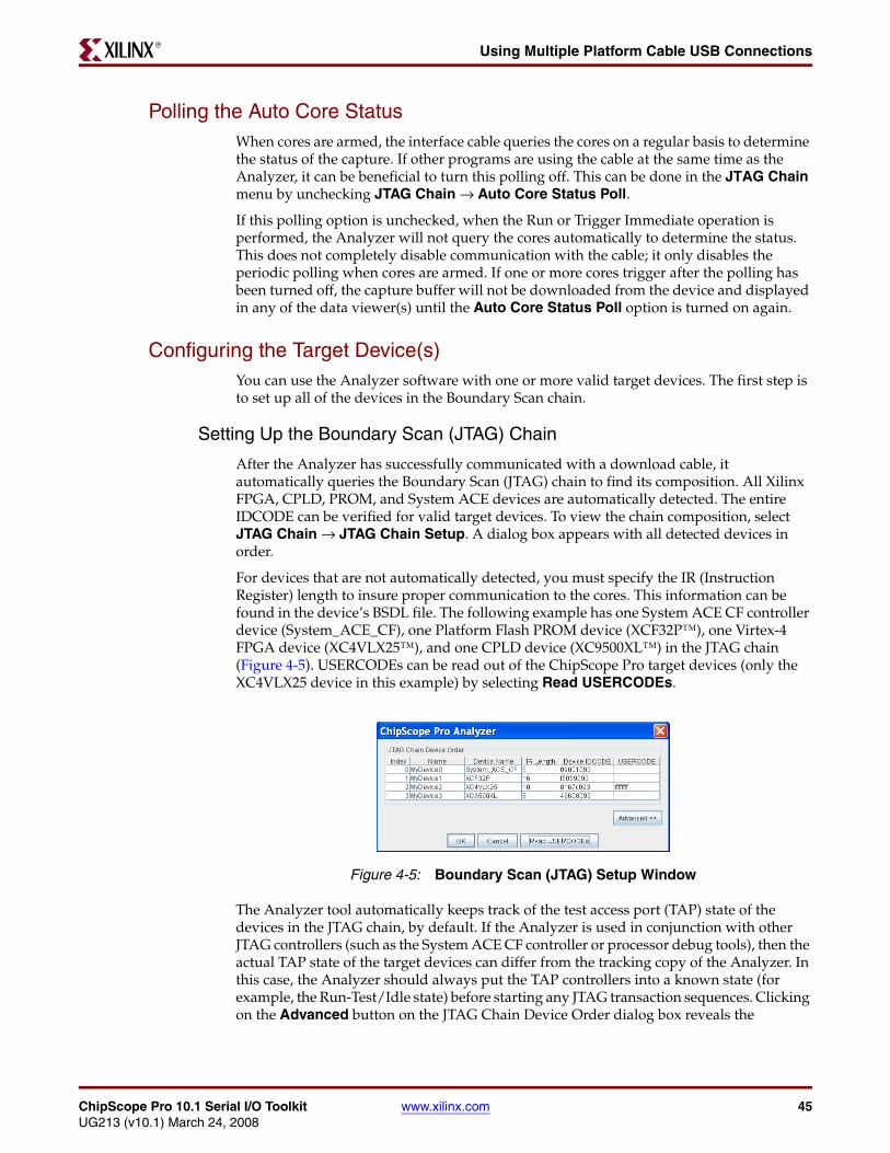
For devices that are not automatically detected, you must specify the IR (Instruction Register) length to insure proper communication to the cores. This information can be found in the device’s BSDL file. The following example has one System ACE CF controller device (System_ACE_CF), one Platform Flash PROM device (XCF32P™), one Virtex-4 FPGA device (XC4VLX25™), and one CPLD device (XC9500XL™) in the JTAG chain (Figure 4-5). USERCODEs can be read out of the ChipScope Pro target devices (only the XC4VLX25 device in this example) by selecting Read USERCODEs.
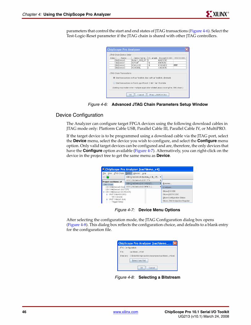
The Analyzer tool automatically keeps track of the test access port (TAP) state of the devices in the JTAG chain, by default. If the Analyzer is used in conjunction with other JTAG controllers (such as the System ACE CF controller or processor debug tools), then the actual TAP state of the target devices can differ from the tracking copy of the Analyzer. In this case, the Analyzer should always put the TAP controllers into a known state (for example, the Run-Test/Idle state) before starting any JTAG transaction sequences. Clicking on the Advanced button on the JTAG Chain Device Order dialog box reveals the
X-Ref Target - Figure 4-5
Figure 4-5: Boundary Scan (JTAG) Setup Window
46 www.xilinx.com ChipScope Pro 10.1 Serial I/O ToolkitUG213 (v10.1) March 24, 2008
Chapter 4: Using the ChipScope Pro AnalyzerR
parameters that control the start and end states of JTAG transactions (Figure 4-6). Select the Test-Logic-Reset parameter if the JTAG chain is shared with other JTAG controllers.
Device Configuration
The Analyzer can configure target FPGA devices using the following download cables in JTAG mode only: Platform Cable USB, Parallel Cable III, Parallel Cable IV, or MultiPRO.
If the target device is to be programmed using a download cable via the JTAG port, select the Device menu, select the device you wish to configure, and select the Configure menu option. Only valid target devices can be configured and are, therefore, the only devices that have the Configure option available (Figure 4-7). Alternatively, you can right-click on the device in the project tree to get the same menu as Device.
After selecting the configuration mode, the JTAG Configuration dialog box opens (Figure 4-8). This dialog box reflects the configuration choice, and defaults to a blank entry for the configuration file.
X-Ref Target - Figure 4-6
Figure 4-6: Advanced JTAG Chain Parameters Setup Window
X-Ref Target - Figure 4-7
Figure 4-7: Device Menu Options
X-Ref Target - Figure 4-8
Figure 4-8: Selecting a Bitstream

ChipScope Pro 10.1 Serial I/O Toolkit www.xilinx.com 47UG213 (v10.1) March 24, 2008
Using Multiple Platform Cable USB ConnectionsR
To select the BIT file to download, click on Select New File. The Open Configuration File dialog box (Figure 4-9) opens. Using the browser, select the device file you want to use to configure the target device. It is important to select a BIT file generated with the proper BitGen settings. Specifically, the -g StartupClk:JtagClk option must be used in BitGen in order for configuration to be successful.
Once you locate and select the proper device file, click Open to return to the JTAG Configuration dialog box (Figure 4-8, page 46).
Once the BIT file has been chosen, click OK to configure the device.
Observing Configuration Progress
While the device is being configured, the status of the configuration is displayed at the bottom of the Analyzer window. If the DONE status is not displayed, a dialog box opens, explaining the problem encountered during configuration. If the download is successful, the target device is automatically queried for cores, and the project tree is updated with the number of cores present. A folder is created for each core unit found and Trigger Setup, Waveform, and Listing leaf nodes appear under each unit. A Bus Plot leaf node appears only if the core unit is determined to be an ILA core.
X-Ref Target - Figure 4-9
Figure 4-9: Opening a Configuration File

48 www.xilinx.com ChipScope Pro 10.1 Serial I/O ToolkitUG213 (v10.1) March 24, 2008
Chapter 4: Using the ChipScope Pro AnalyzerR
Displaying JTAG User and ID Codes
One method of verifying that the target device was configured correctly is to upload the device and user-defined ID codes from the target device. The user-defined ID code is the 8-digit hexadecimal code that can be set using the BitGen option -g UserID.
Note: The IBERT Core Generator does not allow the programming of JTAG User Codes in the target FPGA.
To upload and display the user-defined ID code for a particular device, select the Show USERCODE option from the Device menu for a particular device (Figure 4-7, page 46). Select the Show IDCODE option from the Device menu to display the fixed device ID code for a particular device. The results of these queries are displayed in the messages window (Figure 4-10). The IDCODE and USERCODE can also be displayed in the JTAG Chain Setup dialog box, JTAG Chain → JTAG Chain Setup (Figure 4-5, page 45).
Displaying Configuration Status Information
The 32-bit configuration status register contains information such as status of the configuration pins and other internal signals. If configuration problems occur, select Show Configuration Status from the Device menu for a particular target device to display this information in the messages window (Figure 4-11).
Note: All target devices contain two internal registers that contain status information: 1) The Configuration Status register (32 bits); and 2) the JTAG Instruction register (variable length, depending on the device). Only valid target devices have a Configuration Status register. Although all devices have a JTAG Instruction register that can be read, the implementation of that particular device determines whether any status information is present. Refer to each device’s respective data sheet for more information.
X-Ref Target - Figure 4-10
Figure 4-10: Device USERCODE and IDCODE
X-Ref Target - Figure 4-11
Figure 4-11: Displaying Device Configuration Status

ChipScope Pro 10.1 Serial I/O Toolkit www.xilinx.com 49UG213 (v10.1) March 24, 2008
Using Multiple Platform Cable USB ConnectionsR
For some devices, the JTAG Instruction register also contains status information. Use Device → Show Instruction Register to display this information in the messages window for any device in the JTAG chain (Figure 4-12). X-Ref Target - Figure 4-12
Figure 4-12: Displaying Device Instruction Register Status

50 www.xilinx.com ChipScope Pro 10.1 Serial I/O ToolkitUG213 (v10.1) March 24, 2008
Chapter 4: Using the ChipScope Pro AnalyzerR
IBERT Console Window for Virtex-4 FX DevicesTo open the console for a IBERT core for Virtex-4 FX devices, select Window → New Unit Windows and the core desired (Figure 4-13). A dialog box displays for that core, and you can select the IBERT Console (Figure 4-13). Windows cannot be closed from this dialog box.
The same operation can by achieved by double-clicking on the IBERT Console leaf node in the project tree, or by right-clicking on the IBERT Console leaf node and selecting Open IBERT Console.
The IBERT Console is made up of vertical columns and horizontal sections (see Figure 4-14). Each column represents a specific active RocketIO multi-gigabit transceiver (MGT) in the device. Columns and rows in the table can be reordered by dragging and dropping them. Rows can only be reordered within their own section, they cannot be dragged to other sections.
The horizontal sections are MGT Settings, BERT Settings, TX Settings, and RX Settings. Click on each section heading to collapse or expand that section.
X-Ref Target - Figure 4-13
Figure 4-13: Opening New Unit Windows
X-Ref Target - Figure 4-14
Figure 4-14: IBERT Console with Only MGT Settings Expanded

ChipScope Pro 10.1 Serial I/O Toolkit www.xilinx.com 51UG213 (v10.1) March 24, 2008
Using Multiple Platform Cable USB ConnectionsR
The column header title is the MGT number (for example, MGT105B), and the color of the column header reflects the link status (see Table 4-4).
MGT Settings
The MGT Settings section contains basic control and status information about the given MGT.
MGT Alias
The MGT Alias is a user-definable name for an MGT. It defaults to the MGT number, but clicking on the alias itself allows the user to change the alias into something else.
MGT Location
The MGT Location gives the X and Y coordinates of the MGT in the device, which cannot be changed. The X-Y location is the location used to constrain an MGT design in a UCF file.
MGT Link Status
The MGT Link Status is only a reflection of the receive-side logic. The link status indicates whether the receive logic of the MGT is receiving data that it expects, at the expected data rate. Green means that the link is solid, yellow means that the link is unstable, and red means there is no link at all.
TX Lock and RX Lock
The TX Lock and RX Lock are status lights indicating the lock status of the TX and RX PLLs. Green means it is locked, yellow means the lock status is changing, and red means the PLL is not locked.
MGT Loopback Mode
The MGT Loopback Mode is a control to change the MGT loopback setting. The design is initialized when this control is set to Serial. Serial sets the MGT to do an internal loopback of both the PCS and PMA. The Fabric loopback setting acts as a mirror; that is, the MGT transmits whatever it has received. A link is seen with the Fabric setting only when external text equipment is used.
MGT Channel Reset
The MGT Channel Reset performs a PCS and PMA reset of the given MGT, including the PLLs. Because the TX PLL is shared between both MGTs in the tile (for example, MGT103A and MGT103B), performing an MGT Channel Reset affects both MGTs in the tile.
Table 4-4: MGT Link Status
Color Link Status
Green The MGT is linked (receiving valid data).
YellowThe link is unstable and is rapidly transitioning between linked and not linked status.
Red There is no link.

52 www.xilinx.com ChipScope Pro 10.1 Serial I/O ToolkitUG213 (v10.1) March 24, 2008
Chapter 4: Using the ChipScope Pro AnalyzerR
Edit DRP
All the attributes for an MGT can be viewed or changed via the DRP. Click on the Edit DRP button to bring up that MGT’s Edit DRP dialog (Figure 4-15).
In the Attribute tab, you can choose the attribute you wish to view or change using the DRP Attribute combo box. The attributes are organized alphabetically. After an attribute is chosen, the DRP is read at that moment, and the current value for that attribute is displayed in the Current Value field. The radio buttons on the bottom right of the dialog indicate the radix of the two value fields. To enter in a new value, type it into the Hex or Binary Value field, and click the Apply button. If you want to modify a specific DRP address, and not a specific attribute, click the DRP Address tab. This tab is recommended for advanced users (Figure 4-16).
Choose the address you want to modify in the Address combobox. The current value displays in Hex or Binary, according to the radio buttons. To change the value, type in a new value in the Value field, and a mask in the Mask field. Any combination of bits is masked out. A mask bit of 1 changes the bit; a mask bit of 0 leaves the bit unchanged. Once the value and mask have been entered, click Apply to enter the changes. To dismiss the dialog, click Cancel.
Dump DRP
The attributes of each MGT can be controlled through the Dynamic Reconfiguration Port (DRP). Clicking on the Dump DRP button will read that MGT’s DRP, parse the results into the various attributes, and print the results to the Messages pane. The results of the DRP read also appear in the cs_analyzer log file.
X-Ref Target - Figure 4-15
Figure 4-15: The Edit DRP Dialog
X-Ref Target - Figure 4-16
Figure 4-16: The Address Tab of the Edit DRP Dialog

ChipScope Pro 10.1 Serial I/O Toolkit www.xilinx.com 53UG213 (v10.1) March 24, 2008
Using Multiple Platform Cable USB ConnectionsR
Export UCF
When the Dump DRP function is used, all the attributes for the MGT are printed to the screen. However, they are printed in binary format, and not all attributes are applicable for a user design. When the Export UCF button is clicked, the user is prompted to specify a file location, and a UCF file is written that adheres to the formatting required.
Edit Clock Settings
The line rate settings for each MGT can be changed in-system at runtime. The Edit Clock Settings dialog is used for this task. It’s called the Edit Clock Settings dialog because the setting for all the PLL clock dividers are affected when the line rate is changed. Click on the Edit... button to bring up the Edit Clock dialog (Figure 4-17).
In the first field, type the new line rate in MHz, and click the Set button. The Preferred VCO and REFCLK Freq dialogs will be populated with values. Choose the VCO rate (many times there is only one valid VCO rate), and the REFCLK Frequency. The REFCLK Frequency is the external clock on the board going to the MGTCLK component you chose above. For a given line rate, up to six REFCLK frequencies are available. If your frequency is not listed, see the Virtex-4 FPGA RocketIO Multi-Gigabit Transceiver User Guide [Ref 4] for information on valid line rate and divider settings.
After all the fields are filled out, click Apply to automatically apply the new settings to both the TX and RX PLLs. Because the TX PLL is shared among the two MGTs in a pair, changing the line rate can affect the link status of the other MGT in the pair.
Fabric Width
This is a status field, indicating the width of the data interface between the MGT and the FPGA fabric around it. This is also the width of the pattern generators. The Fabric Width can be either 16, 20, 32, or 40 bits. Line rates of 6 Gb/s or greater are not supported for fabric widths of 16 or 20 bits.
X-Ref Target - Figure 4-17
Figure 4-17: Completed Edit Clock Dialog

54 www.xilinx.com ChipScope Pro 10.1 Serial I/O ToolkitUG213 (v10.1) March 24, 2008
Chapter 4: Using the ChipScope Pro AnalyzerR
BERT Settings
The BERT Settings section contains rows governing the bit error ratio tester (BERT).
RX Bit Error Ratio
The RX Bit Error Ratio field contains the currently calculated bit error ratio for that MGT. It is expressed as an exponent. For instance, 1.000E-12 means that one bit error happens (on average) for every trillion bits received.
RX Line Rate
The RX Line Rate is the calculated line rate for the MGT. It uses the userclk to time the design, so an inaccurate or unstable userclk causes this number to be inaccurate or fluctuate. If there is no link, the RX Line Rate field displays N/A.
RX Received Words
The RX Received Words field contains a running tally of the number of words received. The word size is the same as the Fabric Width. This count resets when the BERT Counter Reset button is pushed.
RX Total Bit Errors
The RX Total Bit Errors field contains a running tally of the number of bit errors detected. This count resets when the BERT Counter Reset button is pushed.
BERT Reset
The BERT Reset button resets the bit error and received words counters. It is appropriate to reset the BERT counters after the MGT is linked and stable.
X-Ref Target - Figure 4-18
Figure 4-18: BERT Settings

ChipScope Pro 10.1 Serial I/O Toolkit www.xilinx.com 55UG213 (v10.1) March 24, 2008
Using Multiple Platform Cable USB ConnectionsR
TX Settings
The TX Settings section controls and displays information about the transmit side of the MGT (Figure 4-19).
TX User Clock Source
The TX User Clock Source field shows which clock is driving the TX logic, for example, the pattern generator. If the TX User Clock Source is not the same MGT as the column indicates, those two MGTs must have the same TX clock settings.
TX PMA Clock Select
The TX PMA Clock Select combos show which MGTCLK component is clocking the TX PLLs. Only two MGTCLK components are available on each side of the device, so only two choices are available.
TX Data Pattern
The TX Data Pattern combo box controls which patterns are sent (TX). The choices for the Basic pattern generator (chosen at Generate time) are 1/2X Clock, 1/10X Clock, 1/20X Clock, and 7 Bit PRBS (using the X7 + X6 + 1 polynomial). The Full pattern generator contains all the Basic patterns, plus 9-, 11-, 15-, 20-, 23-, 29-, and 31-bit PRBS patterns, an alternative 7-bit PRBS pattern (using the X7 + X + 1 polynomial), an Idle (K28.5 ±) pattern, and a framed counter pattern.
TX Encoding
If the Fabric Width of an MGT is either 16 or 32 bits and the MGT has been linked, then 8B/10B encoding/decoding is available. Select 8B/10B in the TX Encoding combo box to turn on encoding.
Invert TX Polarity
The MGT has a port that controls the polarity of all the data sent and received. To flip the polarity of the TX side of the MGT, check the Invert TX Polarity box.
Inject TX Error
The Inject button flips the polarity of only one bit in only one transmitted word. The MGT receiver that is connected to this MGT transmitter should detect a single bit error.
X-Ref Target - Figure 4-19
Figure 4-19: IBERT TX Settings

56 www.xilinx.com ChipScope Pro 10.1 Serial I/O ToolkitUG213 (v10.1) March 24, 2008
Chapter 4: Using the ChipScope Pro AnalyzerR
RX Settings
The RX Settings section controls and displays information about the receive side of the MGT (Figure 4-20).
RX User Clock Source
The RX User clock is always driven by the RXRECCLK1 pin from the MGT. This clock is the recovered clock from the received data.
RX PMA Clock Select
The RX PMA Clock Select combos show which MGTCLK component is clocking the TX PLLs. Only two MGTCLK components are available on each side of the device, so only two choices are available.
RX Data Pattern
The RX Data Pattern combo box controls which patterns are received and checked for by the receiver (RX). The choices for the Basic pattern generator (chosen at Generate time) are 1/2X Clock, 1/10X Clock, 1/20X Clock, and 7 Bit PRBS (using the X7 + X6 + 1 polynomial). The Full pattern generator contains all the Basic patterns, plus 9-, 11-, 15-, 20-, 23-, 29-, and 31-bit PRBS patterns, an alternative 7-bit PRBS pattern (using the X7 + X + 1 polynomial), an Idle (K28.5 ±) pattern, and a framed counter pattern.
RX Decoding
If the Fabric Width of an MGT is either 16 or 32 bits and the MGT has been linked, then 8B/10B encoding/decoding is available. Select 8B/10B in the RX Decoding combo box to turn on decoding.
Invert RX Polarity
The MGT has a port that controls the polarity of all the data sent and received. To flip the polarity of the RX side, check the Invert RX Polarity box.
X-Ref Target - Figure 4-20
Figure 4-20: IBERT RX Settings

ChipScope Pro 10.1 Serial I/O Toolkit www.xilinx.com 57UG213 (v10.1) March 24, 2008
Using Multiple Platform Cable USB ConnectionsR
IBERT Toolbar and Menu Options
Reset All
To reset all the channels in the IBERT core, use IBERT → Reset All or click the Reset All button in the toolbar.
IBERT Console Options
To open the IBERT Console Options window, use IBERT → IBERT Console Options or click the IBERT Console Options button in the toolbar.
JTAG Scan Rate and Scan Now
The JTAG Scan Rate toolbar and IBERT → JTAG Scan Rate menu options are used to select how frequently the Analyzer software queries the IBERT core for status information. The default is 1s between queries, but it can be set to 250 ms, 500 ms, 1s, 2s, 5s, or Manual Scan. When Manual Scan is selected, use IBERT → Scan Now or the Scan Now (or S!) toolbar button to query the IBERT core.
IBERT Options Dialog
To open the IBERT Options dialog (Figure 4-21), either choose IBERT → IBERT Console Options from the menu, or click on the IBERT Console Options button on the toolbar.X-Ref Target - Figure 4-21
Figure 4-21: IBERT Options Dialog
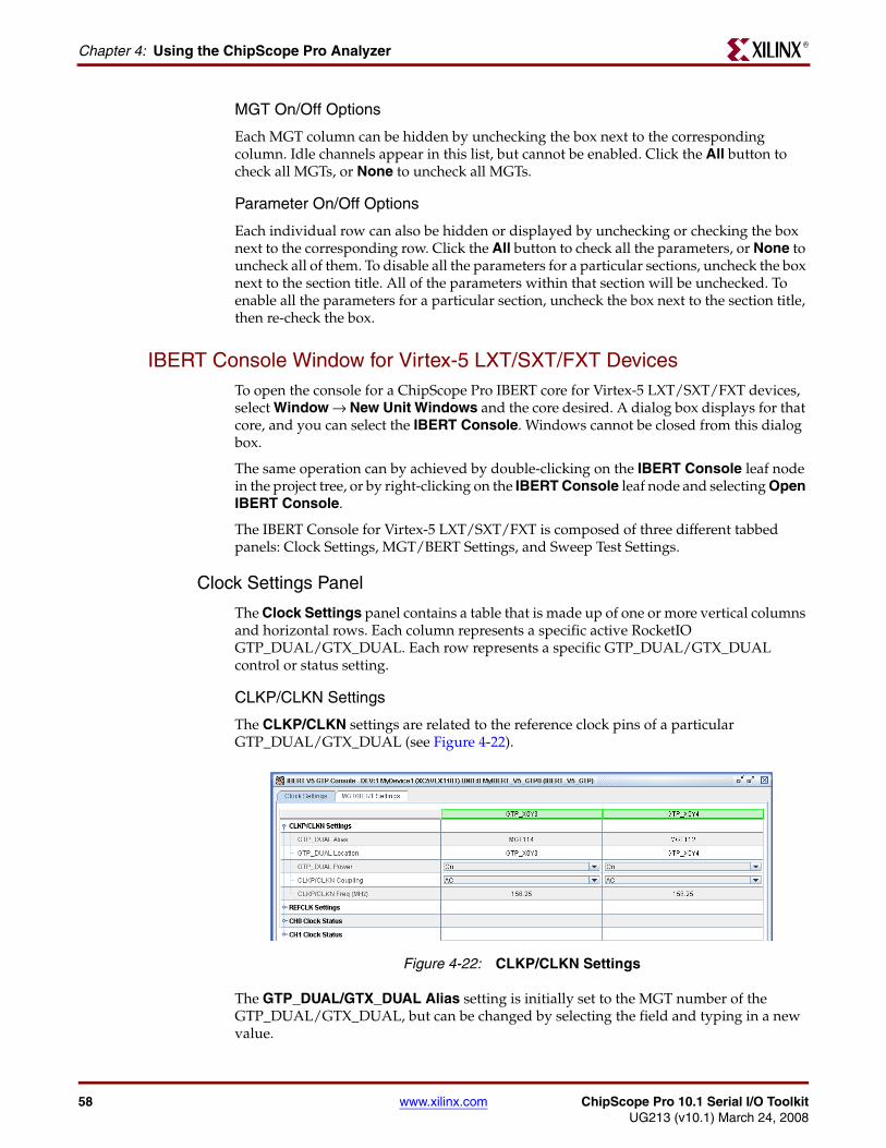
58 www.xilinx.com ChipScope Pro 10.1 Serial I/O ToolkitUG213 (v10.1) March 24, 2008
Chapter 4: Using the ChipScope Pro AnalyzerR
MGT On/Off Options
Each MGT column can be hidden by unchecking the box next to the corresponding column. Idle channels appear in this list, but cannot be enabled. Click the All button to check all MGTs, or None to uncheck all MGTs.
Parameter On/Off Options
Each individual row can also be hidden or displayed by unchecking or checking the box next to the corresponding row. Click the All button to check all the parameters, or None to uncheck all of them. To disable all the parameters for a particular sections, uncheck the box next to the section title. All of the parameters within that section will be unchecked. To enable all the parameters for a particular section, uncheck the box next to the section title, then re-check the box.
IBERT Console Window for Virtex-5 LXT/SXT/FXT DevicesTo open the console for a ChipScope Pro IBERT core for Virtex-5 LXT/SXT/FXT devices, select Window → New Unit Windows and the core desired. A dialog box displays for that core, and you can select the IBERT Console. Windows cannot be closed from this dialog box.
The same operation can by achieved by double-clicking on the IBERT Console leaf node in the project tree, or by right-clicking on the IBERT Console leaf node and selecting Open IBERT Console.
The IBERT Console for Virtex-5 LXT/SXT/FXT is composed of three different tabbed panels: Clock Settings, MGT/BERT Settings, and Sweep Test Settings.
Clock Settings Panel
The Clock Settings panel contains a table that is made up of one or more vertical columns and horizontal rows. Each column represents a specific active RocketIO GTP_DUAL/GTX_DUAL. Each row represents a specific GTP_DUAL/GTX_DUAL control or status setting.
CLKP/CLKN Settings
The CLKP/CLKN settings are related to the reference clock pins of a particular GTP_DUAL/GTX_DUAL (see Figure 4-22).
The GTP_DUAL/GTX_DUAL Alias setting is initially set to the MGT number of the GTP_DUAL/GTX_DUAL, but can be changed by selecting the field and typing in a new value.
X-Ref Target - Figure 4-22
Figure 4-22: CLKP/CLKN Settings

ChipScope Pro 10.1 Serial I/O Toolkit www.xilinx.com 59UG213 (v10.1) March 24, 2008
Using Multiple Platform Cable USB ConnectionsR
The GTP_DUAL/GTX_DUAL Location setting denotes the X/Y coordinate of the GTP_DUAL/GTX_DUAL in the device.
The GTP_DUAL/GTX_DUAL Power setting is used to control the power of the reference clock circuitry of the GTP_DUAL/GTX_DUAL. This power control needs to be set to On to enable any GTP_DUAL/GTX_DUAL functionality. Also, this power control needs to be On for any GTP_DUAL/GTX_DUAL that is participating in reference clock sharing (either as a reference clock source or an intermediate pass-through tile).
The CLKP/CLKN Coupling setting controls the type of coupling used by the GTP_DUAL/GTX_DUAL reference clock pins. The valid settings are AC or DC.
The CLKP/CLKN Freq (MHz) denotes the frequency of the reference clock source that is connected to the CLKP and CLKN pins of the particular GTP_DUAL/GTX_DUAL component. The default value is the reference clock frequency that was specified during IBERT core generation. The frequency value can be changed by selecting the cell in the table and typing in a new value.
REFCLK Settings
The REFCLK settings are related to the reference clock input source and other related parameters of a particular GTP_DUAL/GTX_DUAL (see Figure 4-23).
The REFCLK Input setting allows you to select the reference clock source for a particular GTP_DUAL/GTX_DUAL from any of the valid GTP_DUALs/GTX_DUALs in the system. The following rules apply when selecting reference clock inputs:
1. The reference clock source needs to originate from a GTP_DUAL/GTX_DUAL that is no more than three tiles above or below the destination GTP_DUAL/GTX_DUAL. For instance, the reference clock for GTP_DUAL_X0Y5 can be GTP_DUAL_X0Y2 (which is three tiles away), but cannot be GTP_DUAL_X0Y1 (which is four tiles away).
2. The reference clock source GTP_DUAL/GTX_DUAL, destination GTP_DUAL/GTX_DUAL, and all GTP_DUALs/GTX_DUALs in between must use the same REFCLK Input selection. For instance, in order for GTP_DUAL_X0Y2 to use GTP_DUAL_X0Y0 as the reference clock input source, GTP_DUAL_X0Y1 must also use GTP_DUAL_X0Y0 as the reference clock input source.
3. The GTP_DUAL/GTX_DUAL Power setting for the reference clock source GTP_DUAL/GTX_DUAL, destination GTP_DUAL/GTX_DUAL, and all GTP_DUALs/GTX_DUALs in between must be set to On.
The GTP_DUAL/GTX_DUAL PLL Status indicator shows the lock status of the PLL that is inside of the GTP_DUAL/GTX_DUAL component. The valid states of this status indicator are LOCKED (green) or NOT LOCKED (red).
X-Ref Target - Figure 4-23
Figure 4-23: REFCLK Settings
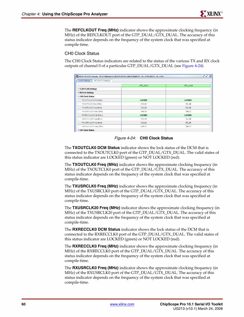
60 www.xilinx.com ChipScope Pro 10.1 Serial I/O ToolkitUG213 (v10.1) March 24, 2008
Chapter 4: Using the ChipScope Pro AnalyzerR
The REFCLKOUT Freq (MHz) indicator shows the approximate clocking frequency (in MHz) of the REFCLKOUT port of the GTP_DUAL/GTX_DUAL. The accuracy of this status indicator depends on the frequency of the system clock that was specified at compile-time.
CH0 Clock Status
The CH0 Clock Status indicators are related to the status of the various TX and RX clock outputs of channel 0 of a particular GTP_DUAL/GTX_DUAL (see Figure 4-24).
The TXOUTCLK0 DCM Status indicator shows the lock status of the DCM that is connected to the TXOUTCLK0 port of the GTP_DUAL/GTX_DUAL. The valid states of this status indicator are LOCKED (green) or NOT LOCKED (red).
The TXOUTCLK0 Freq (MHz) indicator shows the approximate clocking frequency (in MHz) of the TXOUTCLK0 port of the GTP_DUAL/GTX_DUAL. The accuracy of this status indicator depends on the frequency of the system clock that was specified at compile-time.
The TXUSRCLK0 Freq (MHz) indicator shows the approximate clocking frequency (in MHz) of the TXUSRCLK0 port of the GTP_DUAL/GTX_DUAL. The accuracy of this status indicator depends on the frequency of the system clock that was specified at compile-time.
The TXUSRCLK20 Freq (MHz) indicator shows the approximate clocking frequency (in MHz) of the TXUSRCLK20 port of the GTP_DUAL/GTX_DUAL. The accuracy of this status indicator depends on the frequency of the system clock that was specified at compile-time.
The RXRECCLK0 DCM Status indicator shows the lock status of the DCM that is connected to the RXRECCLK0 port of the GTP_DUAL/GTX_DUAL. The valid states of this status indicator are LOCKED (green) or NOT LOCKED (red).
The RXRECCLK0 Freq (MHz) indicator shows the approximate clocking frequency (in MHz) of the RXRECCLK0 port of the GTP_DUAL/GTX_DUAL. The accuracy of this status indicator depends on the frequency of the system clock that was specified at compile-time.
The RXUSRCLK0 Freq (MHz) indicator shows the approximate clocking frequency (in MHz) of the RXUSRCLK0 port of the GTP_DUAL/GTX_DUAL. The accuracy of this status indicator depends on the frequency of the system clock that was specified at compile-time.
X-Ref Target - Figure 4-24
Figure 4-24: CH0 Clock Status

ChipScope Pro 10.1 Serial I/O Toolkit www.xilinx.com 61UG213 (v10.1) March 24, 2008
Using Multiple Platform Cable USB ConnectionsR
The RXUSRCLK20 Freq (MHz) indicator shows the approximate clocking frequency (in MHz) of the RXUSRCLK20 port of the GTP_DUAL/GTX_DUAL. The accuracy of this status indicator depends on the frequency of the system clock that was specified at compile-time.
CH1 Clock Status
The CH1 Clock Status indicators are related to the status of the various RX clock outputs of channel 1 of a particular GTP_DUAL/GTX_DUAL (see Figure 4-25).
The RXRECCLK1 DCM Status indicator shows the lock status of the DCM that is connected to the RXRECCLK1 port of the GTP_DUAL/GTX_DUAL. The valid states of this status indicator are LOCKED (green) or NOT LOCKED (red).
The RXRECCLK1 Freq (MHz) indicator shows the approximate clocking frequency (in MHz) of the RXRECCLK1 port of the GTP_DUAL/GTX_DUAL. The accuracy of this status indicator depends on the frequency of the system clock that was specified at compile-time.
The RXUSRCLK1 Freq (MHz) indicator shows the approximate clocking frequency (in MHz) of the RXUSRCLK1 port of the GTP_DUAL/GTX_DUAL. The accuracy of this status indicator depends on the frequency of the system clock that was specified at compile-time.
The RXUSRCLK21 Freq (MHz) indicator shows the approximate clocking frequency (in MHz) of the RXUSRCLK21 port of the GTP_DUAL/GTX_DUAL. The accuracy of this status indicator depends on the frequency of the system clock that was specified at compile-time.
X-Ref Target - Figure 4-25
Figure 4-25: CH1 Clock Status

62 www.xilinx.com ChipScope Pro 10.1 Serial I/O ToolkitUG213 (v10.1) March 24, 2008
Chapter 4: Using the ChipScope Pro AnalyzerR
MGT/BERT Settings Panel
The MGT/BERT Settings panel contains a table that is made up of one or more vertical columns and horizontal rows. Each column represents a specific active RocketIO GTP/GTX channel. Each row represents a specific GTP/GTX or GTP_DUAL/GTX_DUAL control or status setting.
MGT Settings
The MGT Settings control and status indicators are related to the various settings for a particular GTP_DUAL/GTX_DUAL channel (see Figure 4-26).
The MGT Alias setting is initially set to the MGT and channel number of the GTP/GTX channel, but can be changed by selecting the field and typing in a new value.
The GTP_DUA/GTX_DUAL Location setting denotes the X/Y coordinate of the GTP_DUAL/GTX_DUAL in the device.
The MGT Link Status indicator is displays the status of the link detection logic that is connected to the receiver of a particular GTP/GTX channel. The valid states of this status indicator are LOCKED (green) and NOT LOCKED (red).
The REFCLKOUT PLL Status indicator shows the lock status of the PLL that is connected to the REFCLKOUT port of the GTP_DUAL/GTX_DUAL. The valid states of this status indicator are LOCKED (green) or NOT LOCKED (red).
The Loopback Mode setting is used to control the loopback mode of a particular GTP/GTX channel. The valid choices for loopback mode are:
• None: No feedback path is used.
• Near-End PCS: The circuit is wholly contained within the near-end GTP/GTX channel. It starts at the TX fabric interface, passes through the PCS, and returns immediately to the RX fabric interface without ever passing through the PMA side of the GTP/GTX channel.
• Near-End PMA: The circuit is wholly contained within the near-end GTP/GTX channel. It starts at the TX fabric interface, passes through the PCS, through the PMA, back through the PCS, and returns to the RX fabric interface.
X-Ref Target - Figure 4-26
Figure 4-26: MGT Settings

ChipScope Pro 10.1 Serial I/O Toolkit www.xilinx.com 63UG213 (v10.1) March 24, 2008
Using Multiple Platform Cable USB ConnectionsR
• Far-End PMA: The circuit originates and ends at some external channel endpoint (for example, a piece of test equipment or another device) but passes through the part of the GTP/GTX channel. For this GTP/GTX loopback mode, the signal comes into the RX pins, passes through the PMA circuitry, and returns immediately to the TX pins.
• Far-End PCS: The circuit originates and ends at some external channel endpoint (for example, a piece of test equipment or another device) but passes through part of the GTP/GTX channel. For this GTP/GTX loopback mode, the signal comes into the RX pins, passes through the PMA, through the PCS, back through the PMA, and returns to the TX pins.
• Far-End Fabric: The circuit originates and ends at some external channel endpoint (for example, a piece of test equipment or another device) but passes through the entire GTP/GTX channel and related fabric logic. For this GTP/GTX loopback mode, the signal comes into the RX pins, passes through the PMA and PCS, through a shallow fabric-based FIFO, back through the PCS and PMA, and finally returns to the TX pins.
The Channel Reset button resets the GTP/GTX channel by clearing and resetting all internal PMA and PCS circuitry as well as the related fabric interfaces.
All the attributes for an MGT can be viewed or changed via the Dynamic Reconfiguration Port (DRP). Click on the Edit DRP button to bring up that GTP_DUAL/GTX_DUAL’s Edit DRP dialog (Figure 4-27).
In the By Attribute Name tab, you can choose the attribute you wish to view or change using the Attribute Name combo box. The attributes are organized alphabetically. After an attribute is chosen, the DRP is read at that moment, and the current value for that attribute is displayed in the Current Value field. The radio buttons near the bottom of the dialog indicate the radix of the two value fields. To specify a new value, select the radix type (Binary Value, Hex Value, or UCF Value), enter text into the New Value field, and click the Apply button.
If you want to modify a specific DRP address, and not a specific attribute, click the By DRP Address tab. This tab is recommended for advanced users (Figure 4-28).
X-Ref Target - Figure 4-27
Figure 4-27: The Virtex-5 Edit DRP Dialog
X-Ref Target - Figure 4-28
Figure 4-28: The Address Tab of the Virtex-5 Edit DRP Dialog
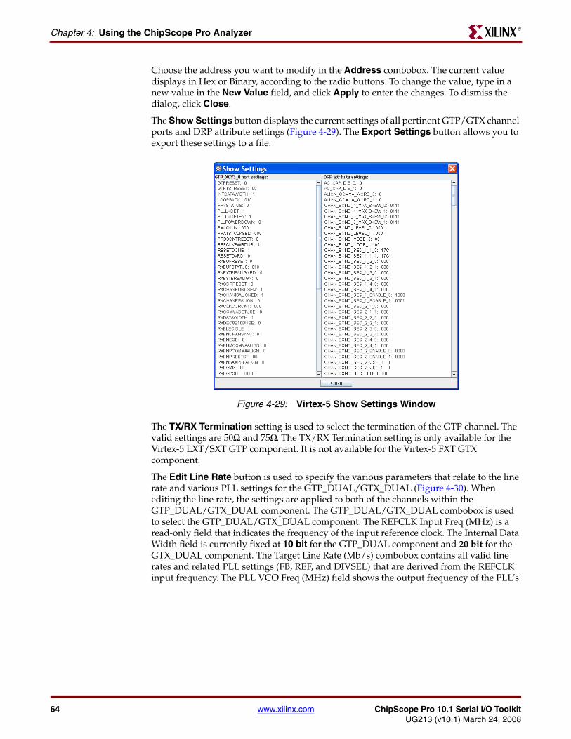
64 www.xilinx.com ChipScope Pro 10.1 Serial I/O ToolkitUG213 (v10.1) March 24, 2008
Chapter 4: Using the ChipScope Pro AnalyzerR
Choose the address you want to modify in the Address combobox. The current value displays in Hex or Binary, according to the radio buttons. To change the value, type in a new value in the New Value field, and click Apply to enter the changes. To dismiss the dialog, click Close.
The Show Settings button displays the current settings of all pertinent GTP/GTX channel ports and DRP attribute settings (Figure 4-29). The Export Settings button allows you to export these settings to a file.
The TX/RX Termination setting is used to select the termination of the GTP channel. The valid settings are 50Ω and 75Ω. The TX/RX Termination setting is only available for the Virtex-5 LXT/SXT GTP component. It is not available for the Virtex-5 FXT GTX component.
The Edit Line Rate button is used to specify the various parameters that relate to the line rate and various PLL settings for the GTP_DUAL/GTX_DUAL (Figure 4-30). When editing the line rate, the settings are applied to both of the channels within the GTP_DUAL/GTX_DUAL component. The GTP_DUAL/GTX_DUAL combobox is used to select the GTP_DUAL/GTX_DUAL component. The REFCLK Input Freq (MHz) is a read-only field that indicates the frequency of the input reference clock. The Internal Data Width field is currently fixed at 10 bit for the GTP_DUAL component and 20 bit for the GTX_DUAL component. The Target Line Rate (Mb/s) combobox contains all valid line rates and related PLL settings (FB, REF, and DIVSEL) that are derived from the REFCLK input frequency. The PLL VCO Freq (MHz) field shows the output frequency of the PLL’s
X-Ref Target - Figure 4-29
Figure 4-29: Virtex-5 Show Settings Window

ChipScope Pro 10.1 Serial I/O Toolkit www.xilinx.com 65UG213 (v10.1) March 24, 2008
Using Multiple Platform Cable USB ConnectionsR
voltage-controlled oscillator (VCO). The table at the bottom of the Edit Line Rate window shows all line rate-related attributes for the GTP_DUAL/GTX_DUAL.
The Coding combobox is used to select the type of encoding and decoding used by the TX and RX sides of the GTP/GTX channel, respectively. The valid selections are None and 8B/10B.
TX Settings
The TX Settings control and status indicators are related to the various TX settings for a particular GTP/GTX channel (see Figure 4-31).
The TXOUTCLK DCM Status indicator shows the lock status of the DCM that is connected to the TXOUTCLK0 port of the GTP_DUAL/GTX_DUAL. The valid states of this status indicator are LOCKED (green) or NOT LOCKED (red).
The Invert TX Polarity setting controls the polarity of the data sent out of the TX pins of the GTP/GTX channel. To flip the polarity of the TX side of the GTP/GTX, check the Invert TX Polarity box.
The Inject TX Bit Error button inverts the polarity of a single bit in a single transmitted word. The receiver endpoint of the channel that is connected to this transmitter should detect a single bit error.
X-Ref Target - Figure 4-30
Figure 4-30: The Virtex-5 Edit Line Rate Window
X-Ref Target - Figure 4-31
Figure 4-31: Virtex-5 LXT/SXT TX Settings

66 www.xilinx.com ChipScope Pro 10.1 Serial I/O ToolkitUG213 (v10.1) March 24, 2008
Chapter 4: Using the ChipScope Pro AnalyzerR
The TX Diff Boost combobox controls the state of the TX_DIFF_BOOST attribute that is used to enhance the TX Diff Output Swing (also known as the transmitter differential output swing controlled by the TXDIFFCTRL and TXBUFDIFFCTRL ports) and TX Pre-Emphasis (also known as the transmitter pre-emphasis controlled by the TXPREEMPHASIS ports) port settings of the GTP/GTX channel. The TX Diff Boost control is only available for the Virtex-5 LXT/SXT GTP component. It is not available for the Virtex-5 FXT GTX component. For valid combinations of values for these settings, refer to the Virtex-5 FPGA RocketIO GTP Transceiver User Guide [Ref 5] or the Virtex-5 FPGA RocketIO GTX Transceiver User Guide [Ref 6].
RX Settings
The TX Settings control and status indicators are related to the various TX settings for a particular GTP/GTX channel (see Figure 4-32).
The RXOUTCLK DCM Status indicator shows the lock status of the DCM that is connected to the RXOUTCLK port of the GTP/GTX channel. The valid states of this status indicator are LOCKED (green) or NOT LOCKED (red).
The Invert RX Polarity setting controls the polarity of the data received from the RX pins of the GTP/GTX channel. To flip the polarity of the RX side of the GTP/GTX, check the Invert RX Polarity box.
The RX Coupling and RX Termination Voltage settings work together to control the coupling and termination networks of the GTP/GTX channel receiver. For valid combinations of values for these two settings, refer to the Virtex-5 FPGA RocketIO GTP Transceiver User Guide [Ref 5] or the Virtex-5 FPGA RocketIO GTX Transceiver User Guide [Ref 6].
The Enable RX EQ check box enables the receiver equalization of the GTP/GTX channel. If receive equalization is enabled, then you can use the RX EQ WB/HP Ratio and RX EQ HP Pole Loc settings to control the wide-band/high-pass filter ratio and high-pass filter pole location of the GTP/GTX channel receiver, respectively. For valid combinations of values for these two settings, refer to the Virtex-5 FPGA RocketIO GTP Transceiver User Guide [Ref 5] or the Virtex-5 FPGA RocketIO GTX Transceiver User Guide [Ref 6].
X-Ref Target - Figure 4-32
Figure 4-32: Virtex-5 LXT/SXT RX Settings
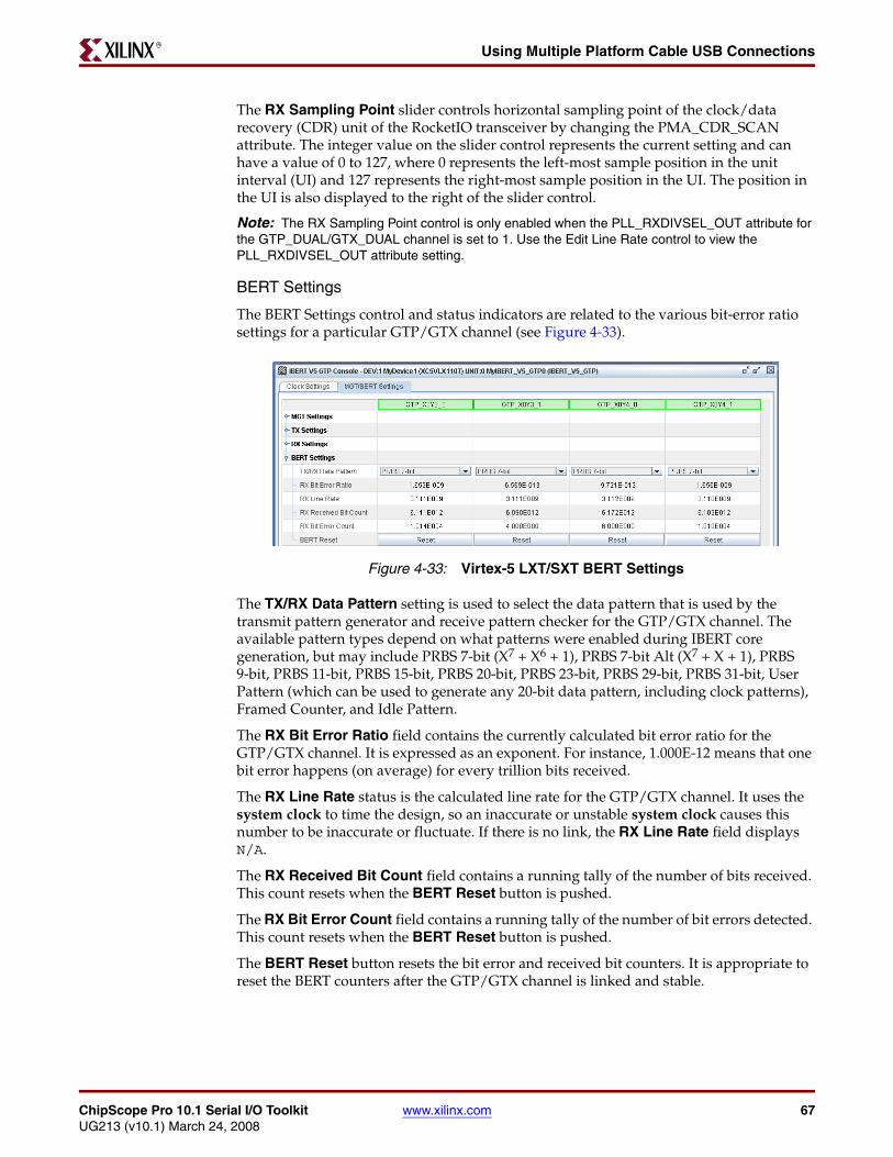
ChipScope Pro 10.1 Serial I/O Toolkit www.xilinx.com 67UG213 (v10.1) March 24, 2008
Using Multiple Platform Cable USB ConnectionsR
The RX Sampling Point slider controls horizontal sampling point of the clock/data recovery (CDR) unit of the RocketIO transceiver by changing the PMA_CDR_SCAN attribute. The integer value on the slider control represents the current setting and can have a value of 0 to 127, where 0 represents the left-most sample position in the unit interval (UI) and 127 represents the right-most sample position in the UI. The position in the UI is also displayed to the right of the slider control.
Note: The RX Sampling Point control is only enabled when the PLL_RXDIVSEL_OUT attribute for the GTP_DUAL/GTX_DUAL channel is set to 1. Use the Edit Line Rate control to view the PLL_RXDIVSEL_OUT attribute setting.
BERT Settings
The BERT Settings control and status indicators are related to the various bit-error ratio settings for a particular GTP/GTX channel (see Figure 4-33).
The TX/RX Data Pattern setting is used to select the data pattern that is used by the transmit pattern generator and receive pattern checker for the GTP/GTX channel. The available pattern types depend on what patterns were enabled during IBERT core generation, but may include PRBS 7-bit (X7 + X6 + 1), PRBS 7-bit Alt (X7 + X + 1), PRBS 9-bit, PRBS 11-bit, PRBS 15-bit, PRBS 20-bit, PRBS 23-bit, PRBS 29-bit, PRBS 31-bit, User Pattern (which can be used to generate any 20-bit data pattern, including clock patterns), Framed Counter, and Idle Pattern.
The RX Bit Error Ratio field contains the currently calculated bit error ratio for the GTP/GTX channel. It is expressed as an exponent. For instance, 1.000E-12 means that one bit error happens (on average) for every trillion bits received.
The RX Line Rate status is the calculated line rate for the GTP/GTX channel. It uses the system clock to time the design, so an inaccurate or unstable system clock causes this number to be inaccurate or fluctuate. If there is no link, the RX Line Rate field displays N/A.
The RX Received Bit Count field contains a running tally of the number of bits received. This count resets when the BERT Reset button is pushed.
The RX Bit Error Count field contains a running tally of the number of bit errors detected. This count resets when the BERT Reset button is pushed.
The BERT Reset button resets the bit error and received bit counters. It is appropriate to reset the BERT counters after the GTP/GTX channel is linked and stable.
X-Ref Target - Figure 4-33
Figure 4-33: Virtex-5 LXT/SXT BERT Settings

68 www.xilinx.com ChipScope Pro 10.1 Serial I/O ToolkitUG213 (v10.1) March 24, 2008
Chapter 4: Using the ChipScope Pro AnalyzerR
Sweep Test Settings Panel
The Sweep Test Settings panel is used to set up a channel test that sweeps through various Virtex-5 RocketIO GTP and GTX transceiver settings. This feature is not available for Virtex-4 FX transceivers. The TX and RX settings are for the same RocketIO transceiver. Sweeping through both TX and RX settings will only work if the transceiver is set to one of the near-end or external loopback modes. Sweeping through RX parameters only can be performed when the corresponding TX endpoint for the link resides in a different device or a different transceiver in the same device.
The Sweep Test Settings tabbed panel is shown in Figure 4-34. It consists of two sections: the Sweep Test Setup and Sweep Test Results sub-panels.
X-Ref Target - Figure 4-34
Figure 4-34: Sweep Test Settings Panel

ChipScope Pro 10.1 Serial I/O Toolkit www.xilinx.com 69UG213 (v10.1) March 24, 2008
Using Multiple Platform Cable USB ConnectionsR
Sweep Test Setup
Setting up the sweep test involves selecting parameters to sweep through, setting up the sweep test result file, and selecting the time per sweep iteration.
Setting Up Sweep Parameters
The RocketIO transceiver parameters that are available for sweep include the following:
• TX Diff Boost (available for GTP only)
• TX Diff Output Swing
• TX Pre-Emphasis
• RX EQ Enable
• RX EQ WB/HP Ratio
• RX EQ HP Pole Loc
• RX Sampling Point
The sweep parameters can be initialized in one of two ways:
• Click the Clear All Parameters button to clear all parameters to the Select… option.
• Click the Set Parameters to Current Values button to set the parameters to their current values on the MGT/BERT Settings panel.
The order of the parameters in the Sweep Parameter table dictates how the parameters will be swept. The values of the parameters near the top of the table are swept less frequently than the parameters near the bottom of the table. In other words, the parameters near the top of the table are in the outer loops of the sweep algorithm while the parameters near the bottom of the table are in the inner loops of the sweep algorithm. The order of the parameters in the table cannot be changed.
Each parameter must be set up with a start and end value. The order of the parameter values cannot be changed. Once you select the start value, the end values available for selection will change automatically to include only valid selections. If you do not want to sweep through a parameter, set the start and end values for that parameter to the same value. The Sweep Value Count column indicates how many values will be swept through for a particular parameter. Once all sweep parameters have valid start and end values, the total number of sweep iterations are shown in the Total Iterations field.
Setting Up Sweep Test Result File
The results from a sweep test are displayed in the Sweep Test Status panel and are also sent to a sweep test result file. Clicking on the Sweep Test Result File Settings button brings up the dialog window shown in Figure 4-35.
The location of the file and the number of sweep iterations stored in each file can both be set by the user. If the total number of sweep iterations exceeds the file limit, multiple files
X-Ref Target - Figure 4-35
Figure 4-35: Sweep Test Result File Settings

70 www.xilinx.com ChipScope Pro 10.1 Serial I/O ToolkitUG213 (v10.1) March 24, 2008
Chapter 4: Using the ChipScope Pro AnalyzerR
with starting iteration number appended to the base file name will be created in the same directory as the initial result file.
Sweep Test Results
After the sweep test has been set up, the test can be started by clicking the Start button. Once the Start button is clicked, the sweep parameter table will be disabled and the test will start running as shown in Figure 4-36.
As the sweep test runs, the current sweep result file, current iteration, elapsed time, and estimated time remaining status indicators are displayed. The sweep results are shown in the text area near the bottom of the screen. The sweep test can be paused by clicking on the Pause button or stopped completely by clicking on the Reset button.
X-Ref Target - Figure 4-36
Figure 4-36: Sweep Test Results
ChipScope Pro 10.1 Serial I/O Toolkit www.xilinx.com 71UG213 (v10.1) March 24, 2008
Using Multiple Platform Cable USB ConnectionsR
IBERT Toolbar and Menu Options
Reset All
To reset all the channels in the IBERT core, use IBERT_V5GTP/GTX → Reset All or click the Reset All button in the toolbar.
JTAG Scan Rate and Scan Now
The JTAG Scan Rate toolbar and IBERT_V5GTP/GTX → JTAG Scan Rate menu options are used to select how frequently the Analyzer software queries the IBERT core for status information. The default is 1s between queries, but it can be set to 250 ms, 500 ms, 1s, 2s, 5s, or Manual Scan. When Manual Scan is selected, use IBERT_V5GTP/GTX → Scan Now or the Scan Now (or S!) toolbar button to query the IBERT core.
Help
Viewing the Help Pages
The Analyzer help pages contain information for only the currently opened versions of the software and each of the core units. Selecting Help → About: ChipScope Software displays the version of the software. Selecting Help → About: Cores displays detailed core parameters for every detected core. Individual core parameters can be displayed by right-clicking on the unit in the project tree and selecting Show Core Info.
You do not need to reinstall the tools to convert your evaluation version to a full version. You can register an evaluation version of the Analyzer by selecting the Help → Register ChipScope Pro menu option and typing in the appropriate full-version registration ID. More information on how to obtain a full version of ChipScope Pro software is available from the ChipScope Pro Products page [Ref 10].
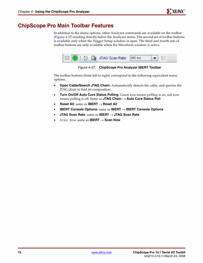
72 www.xilinx.com ChipScope Pro 10.1 Serial I/O ToolkitUG213 (v10.1) March 24, 2008
Chapter 4: Using the ChipScope Pro AnalyzerR
ChipScope Pro Main Toolbar FeaturesIn addition to the menu options, other Analyzer commands are available on the toolbar (Figure 4-37) residing directly below the Analyzer menu. The second set of toolbar buttons is available only when the Trigger Setup window is open. The third and fourth sets of toolbar buttons are only available when the Waveform window is active.
The toolbar buttons (from left to right) correspond to the following equivalent menu options:
• Open Cable/Search JTAG Chain: Automatically detects the cable, and queries the JTAG chain to find its composition
• Turn On/Off Auto Core Status Polling: Green icon means polling is on, red icon means polling is off. Same as JTAG Chain → Auto Core Status Poll
• Reset All: same as IBERT → Reset All
• IBERT Console Options: same as IBERT → IBERT Console Options
• JTAG Scan Rate: same as IBERT → JTAG Scan Rate
• Scan Now: same as IBERT → Scan Now
X-Ref Target - Figure 4-37
Figure 4-37: ChipScope Pro Analyzer IBERT Toolbar

ChipScope Pro 10.1 Serial I/O Toolkit www.xilinx.com 73UG213 (v10.1) March 24, 2008
ChipScope Pro Analyzer Command Line OptionsR
ChipScope Pro Analyzer Command Line OptionsOn Windows systems, the Analyzer can be started either from the command line or from the Start menu.
• On Windows systems, you can invoke the analyzer from the command line by running:
♦ $CHIPSCOPE\analzyer.exe
• On Linux systems, you can invoke the analyzer from the command line by running:
♦ $CHIPSCOPE/bin/lin/analzyer.sh
where $CHIPSCOPE is the installation location.
Optional Arguments
The following command line options are available, if run from the command line:
-geometry <width>x<height>+<left edge x coord>+<top edge y coord>
Set location, width and height of the Analyzer program window.
-project <path and filename>
Reads in specified project file at start. Default is not to read a project file at start up.
-init <path and filename>
Read specified init file at start up and write to the same file when the Analyzer exits. The default is: %userprofile%\.chipscope\cs_analyzer.ini
-log <path and filename>
-log stdout
Write log messages to the specified file. Specifying stdout will write to standard output. The default is: $HOME/.chipscope/cs_analyzer.log
Windows Command Line Example
C:\Xilinx\10.1\ChipScope\bin\nt\analyzer.exe -log c:\proj\t\t.log -init C:\proj\t\t.ini -project c:\proj\t\t.cpj -geometry 1000x300+30+600

74 www.xilinx.com ChipScope Pro 10.1 Serial I/O ToolkitUG213 (v10.1) March 24, 2008
Chapter 4: Using the ChipScope Pro AnalyzerR
ChipScope Pro 10.1 Serial I/O Toolkit www.xilinx.com 75UG213 (v10.1) March 24, 2008
R
Chapter 5
ChipScope Engine JTAG Tcl Interface
OverviewThis interface provides Tcl scripting access to JTAG download cables via the ChipScope Engine JTAG (CseJtag) communication library. The purpose of the CseJtag Tcl interface is to provide a simple scripting system to access basic JTAG functions. In a few lines of Tcl script, you can scan and manipulate the JTAG chain through standard Xilinx cables.
For more information on how to use the CseJtag Tcl interface, see the ChipScope Pro 10.1 Software and Cores User Guide [Ref 1].

76 www.xilinx.com ChipScope Pro 10.1 Serial I/O ToolkitUG213 (v10.1) March 24, 2008
Chapter 5: ChipScope Engine JTAG Tcl InterfaceR

ChipScope Pro 10.1 Serial I/O Toolkit www.xilinx.com 77UG213 (v10.1) March 24, 2008
R
Appendix A
References
Documents specific to ChipScope Pro software and cores:
1. UG029,ChipScope Pro 10.1 Software and Cores User Guide
2. DS282, ChipScope OPB IBA Data Sheet
3. DS283, ChipScope PLB IBA Data Sheet
Documents specific to RocketIO transceivers:
4. UG076, Virtex-4 FPGA RocketIO Multi-Gigabit Transceiver User Guide
5. UG196, Virtex-5 FPGA RocketIO GTP Transceiver User Guide
6. UG198, Virtex-5 FPGA RocketIO GTX Transceiver User Guide
Other references:
7. ActiveState
Xilinx Tools and Solutions
8. ISE Software Manuals
9. EDK Platform Studio Online Help
10. ChipScope Pro Tools and Software


![í ChipScope Pro Software and Cores - Xilinx...User Guide [] UG029 (v14.3) October 16, 2012 [] í ChipScope Pro Software and Cores User Guide UG029 (v14.3) October 16, 2012 This document](https://img.dokumen.tips/doc/110x75/6009e0e96935ee13bd57fbc9/-chipscope-pro-software-and-cores-xilinx-user-guide-ug029-v143-october.jpg)