Embed Size (px)
Citation preview

LogiCORE IP AXI to APB Bridge v2.0
Product Guide for Vivado Design Suite
PG073 October 2, 2013

AXI to APB Bridge v2.0 www.xilinx.com 2PG073 October 2, 2013
Table of Contents
IP Facts
Chapter 1: Overview
Feature Summary. . . . . . . . . . . . . . . . . . . . . . . . . . . . . . . . . . . . . . . . . . . . . . . . . . . . . . . . . . . . . . . . . . 5
Licensing and Ordering Information . . . . . . . . . . . . . . . . . . . . . . . . . . . . . . . . . . . . . . . . . . . . . . . . . . . 5
Chapter 2: Product Specification
Standards Compliance . . . . . . . . . . . . . . . . . . . . . . . . . . . . . . . . . . . . . . . . . . . . . . . . . . . . . . . . . . . . . . 7
Resource Utilization. . . . . . . . . . . . . . . . . . . . . . . . . . . . . . . . . . . . . . . . . . . . . . . . . . . . . . . . . . . . . . . . 7
Port Descriptions . . . . . . . . . . . . . . . . . . . . . . . . . . . . . . . . . . . . . . . . . . . . . . . . . . . . . . . . . . . . . . . . . . 7
Chapter 3: Designing with the Core
General Design Guidelines . . . . . . . . . . . . . . . . . . . . . . . . . . . . . . . . . . . . . . . . . . . . . . . . . . . . . . . . . 12
Clocking. . . . . . . . . . . . . . . . . . . . . . . . . . . . . . . . . . . . . . . . . . . . . . . . . . . . . . . . . . . . . . . . . . . . . . . . . 13
Resets . . . . . . . . . . . . . . . . . . . . . . . . . . . . . . . . . . . . . . . . . . . . . . . . . . . . . . . . . . . . . . . . . . . . . . . . . . 13
Timing Diagram . . . . . . . . . . . . . . . . . . . . . . . . . . . . . . . . . . . . . . . . . . . . . . . . . . . . . . . . . . . . . . . . . . 14
Chapter 4: Customizing and Generating the Core
Vivado Integrated Design Environment . . . . . . . . . . . . . . . . . . . . . . . . . . . . . . . . . . . . . . . . . . . . . . . 15
Output Generation. . . . . . . . . . . . . . . . . . . . . . . . . . . . . . . . . . . . . . . . . . . . . . . . . . . . . . . . . . . . . . . . 17
Chapter 5: Simulation
Chapter 6: Synthesis and Implementation
Chapter 7: Example Design
Overview . . . . . . . . . . . . . . . . . . . . . . . . . . . . . . . . . . . . . . . . . . . . . . . . . . . . . . . . . . . . . . . . . . . . . . . 20
Implementing the Example Design. . . . . . . . . . . . . . . . . . . . . . . . . . . . . . . . . . . . . . . . . . . . . . . . . . . 21
Example Design Directory Structure. . . . . . . . . . . . . . . . . . . . . . . . . . . . . . . . . . . . . . . . . . . . . . . . . . 21
Simulating the Example Design. . . . . . . . . . . . . . . . . . . . . . . . . . . . . . . . . . . . . . . . . . . . . . . . . . . . . . 22
Send Feedback

AXI to APB Bridge v2.0 www.xilinx.com 3PG073 October 2, 2013
Chapter 8: Test Bench
Appendix A: Migrating and Upgrading
Migrating to the Vivado Design Suite. . . . . . . . . . . . . . . . . . . . . . . . . . . . . . . . . . . . . . . . . . . . . . . . . 25
Upgrading in the Vivado Design Suite . . . . . . . . . . . . . . . . . . . . . . . . . . . . . . . . . . . . . . . . . . . . . . . . 25
Appendix B: Debugging
Finding Help on Xilinx.com . . . . . . . . . . . . . . . . . . . . . . . . . . . . . . . . . . . . . . . . . . . . . . . . . . . . . . . . . 26
Debug Tools . . . . . . . . . . . . . . . . . . . . . . . . . . . . . . . . . . . . . . . . . . . . . . . . . . . . . . . . . . . . . . . . . . . . . 28
Appendix C: Additional Resources
Xilinx Resources . . . . . . . . . . . . . . . . . . . . . . . . . . . . . . . . . . . . . . . . . . . . . . . . . . . . . . . . . . . . . . . . . . 29
References . . . . . . . . . . . . . . . . . . . . . . . . . . . . . . . . . . . . . . . . . . . . . . . . . . . . . . . . . . . . . . . . . . . . . . 29
Revision History . . . . . . . . . . . . . . . . . . . . . . . . . . . . . . . . . . . . . . . . . . . . . . . . . . . . . . . . . . . . . . . . . . 30
Notice of Disclaimer. . . . . . . . . . . . . . . . . . . . . . . . . . . . . . . . . . . . . . . . . . . . . . . . . . . . . . . . . . . . . . . 30
Send Feedback
AXI to APB Bridge v2.0 www.xilinx.com 4PG073 October 2, 2013 Product Specification
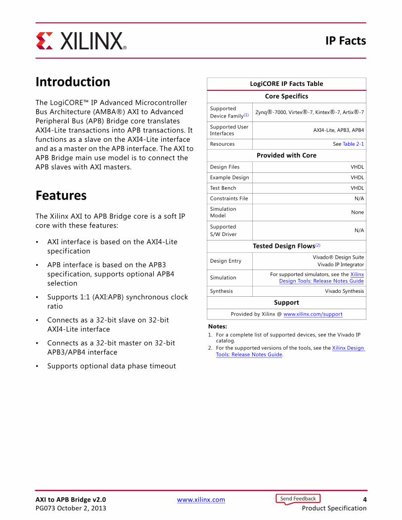
Introduction
The LogiCORE™ IP Advanced Microcontroller Bus Architecture (AMBA®) AXI to Advanced Peripheral Bus (APB) Bridge core translates AXI4-Lite transactions into APB transactions. It functions as a slave on the AXI4-Lite interface and as a master on the APB interface. The AXI to APB Bridge main use model is to connect the APB slaves with AXI masters.
Features
The Xilinx AXI to APB Bridge core is a soft IP core with these features:
• AXI interface is based on the AXI4-Lite specif ication
• APB interface is based on the APB3 specif ication, supports optional APB4 selection
• Supports 1:1 (AXI:APB) synchronous clock ratio
• Connects as a 32-bit slave on 32-bit AXI4-Lite interface
• Connects as a 32-bit master on 32-bit APB3/APB4 interface
• Supports optional data phase timeout
IP Facts
LogiCORE IP Facts Table
Core Specifics
Supported Device Family(1) Zynq®-7000, Virtex®-7, Kintex®-7, Artix®-7
Supported User Interfaces AXI4-Lite, APB3, APB4
Resources See Table 2-1
Provided with Core
Design Files VHDL
Example Design VHDL
Test Bench VHDL
Constraints File N/A
Simulation Model None
Supported S/W Driver
N/A
Tested Design Flows(2)
Design EntryVivado® Design Suite
Vivado IP Integrator
Simulation For supported simulators, see the XilinxDesign Tools: Release Notes Guide
Synthesis Vivado Synthesis
Support
Provided by Xilinx @ www.xilinx.com/support
Notes: 1. For a complete list of supported devices, see the Vivado IP
catalog.2. For the supported versions of the tools, see the Xilinx Design
Tools: Release Notes Guide.
Send Feedback

AXI to APB Bridge v2.0 www.xilinx.com 5PG073 October 2, 2013
Chapter 1
OverviewThe main function of the LogiCORE™ IP AXI to Advanced Peripheral Bus (APB) Bridge core is to connect APB slaves to AXI masters. It translates AXI4-Lite transactions into APB transactions.
Feature SummaryThe 32-bit AXI4-Lite interface on the AXI to APB Bridge core is based on the AMBA AXI and ACE Protocol Specification v2.0 [Ref 1]. The core functions as a 32-bit slave on this interface.
The 32-bit APB interface of the core is based on the AP3 interface as described in the AMBA APB Protocol Specification v2.0 [Ref 1]. The core supports the optional APB4 interface as well. The core functions as a 32-bit master on the APB3/APB4 interface.
The AXI to APB Bridge core supports a 1:1 (AXI:APB) synchronous clock ratio as well as data phase timeout.
Licensing and Ordering InformationThis Xilinx LogiCORE IP module is provided at no additional cost with the Xilinx Vivado® Design Suite under the terms of the Xilinx End User License.
Information about this and other Xilinx LogiCORE IP modules is available at the Xilinx Intellectual Property page. For information on pricing and availability of other Xilinx LogiCORE IP modules and tools, contact your local Xilinx sales representative.
Send Feedback

AXI to APB Bridge v2.0 www.xilinx.com 6PG073 October 2, 2013
Chapter 2
Product SpecificationThe AXI to APB Bridge core translates AXI4-Lite transactions into APB transactions. The bridge functions as a slave on the AXI4-Lite interface and as a master on the APB interface.
The AXI to APB Bridge core block diagram, shown in Figure 2-1, is described in subsequent sections.
AXI4‐Lite Slave Interface
The AXI4-Lite Slave Interface module provides a bidirectional slave interface to the AXI. The AXI address and data bus widths are always fixed to 32 bits. When both write and read transfers are simultaneously requested on AXI4-Lite, the read request is given more priority than the write request. This module also contains the data phase timeout logic for generating a SLVERR response on the AXI interface when an APB slave does not respond.
APB Master Interface
The APB Master module provides the APB master interface on the APB. This interface can be APB3 or APB4, which can be selected by setting the generic for APB protocol. When it is set to APB4, the m_apb_pstrb and m_apb_pprot signals are driven at the APB interface. The APB address and data bus widths are f ixed to 32 bits.
X-Ref Target - Figure 2-1
Figure 2‐1: AXI to APB Bridge Core Block Diagram
AXI4-LiteSlave
Interface
APB Master
Interface
AXI4-Lite
AddressDecoder
Multiplexer
APB3/APB4
DS759_01
Send Feedback

AXI to APB Bridge v2.0 www.xilinx.com 7PG073 October 2, 2013
Chapter 2: Product Specification
Standards ComplianceThe AXI to APB Bridge core is based on the AMBA® AXI4-Lite specification [Ref 1] and the APB3/APB4 specif ication [Ref 1].
Resource UtilizationBecause the AXI to APB Bridge module is used with other design pieces in the FPGA, the resource utilization and timing numbers reported in this section are estimates only. When the AXI to APB Bridge core is combined with other pieces of the FPGA design, the utilization of FPGA resources and timing of the design varies from the results reported here.
The AXI to APB Bridge core resource utilization benchmarks for several parameter combinations, measured with 7 Series FPGAs as the target device, are shown in Table 2-1.
Note: Performance and utilization numbers for Zynq®-7000 devices are expected to be similar to those for 7 Series devices.
Port DescriptionsTable 2-2 shows the I/O signals of the AXI to APB Bridge core.
Table 2‐1: Performance and Resource Utilization Benchmarks 7 Series FPGAs
Parameter Values (other parameters at default value) Device Resources Performance
Number of slaves APB Protocol Timeout value Slices Slice Flip-Flops LUTs FMAX (MHz)
1 APB4 64 119 364 286 200
4 APB4 64 136 370 372 200
8 APB4 64 174 386 475 200
16 APB3 64 181 402 549 200
Table 2‐2: I/O Signal Description
Signal Name Interface I/OInitial State
Description
AXI Interface System Signals
s_axi_aclk System I - AXI clock.
s_axi_aresetn System I - AXI reset, active-Low.
AXI Write Address Channel Signals
Send Feedback

AXI to APB Bridge v2.0 www.xilinx.com 8PG073 October 2, 2013
Chapter 2: Product Specification
s_axi_awaddr[31:0] AXI4-Lite I -AXI Write address. The write address bus gives the address of the f irst transfer in a write burst transaction.
s_axi_awprot[2:0](1) AXI4-Lite I -
Protection type. This signal indicates the normal, privileged, or secure protection level of the write transaction and whether the transaction is a data access or an instruction access. The default value is normal non secure data access.
s_axi_awvalid AXI4-Lite I -Write address valid. This signal indicates that valid write address and control information are available.
s_axi_awready AXI4-Lite O 0Write address ready. This signal indicates that the slave is ready to accept an address and associated control signals.
AXI Write Data Channel Signals
s_axi_wdata[31:0] AXI4-Lite I - Write data bus
s_axi_wstb[3:0](1)AXI4-Lite I - Write strobes. This signal indicates which
byte lanes to update in memory.
s_axi_wvalid AXI4-Lite I - Write valid. This signal indicates that valid write data and strobes are available.
s_axi_wready AXI4-Lite O 0 Write ready. This signal indicates that the slave can accept the write data.
AXI Write Response Channel Signals
s_axi_bresp[1:0] AXI4-Lite O 0 Write response. This signal indicates the status of the write transaction.
s_axi_bvalid AXI4-Lite O 0 Write response valid. This signal indicates that a valid write response is available.
s_axi_bready AXI4-Lite I - Response ready. This signal indicates that the master can accept the response information.
AXI Read Address Channel Signals
s_axi_araddr[31:0] AXI4-Lite I - Read address. The read address bus gives the initial address of a read burst transaction.
s_axi_arprot[2:0](1) AXI4-Lite I -
Protection type. This signal provides protection unit information for the read transaction. The default value is normal non secure data access.
s_axi_arvalid AXI4-Lite I -
Read address valid. When High, this signal indicates that the read address and control information is valid and remains stable until the address acknowledgement signal, s_axi_arredy, is High.
Table 2‐2: I/O Signal Description (Cont’d)
Signal Name Interface I/O Initial State
Description
Send Feedback

AXI to APB Bridge v2.0 www.xilinx.com 9PG073 October 2, 2013
Chapter 2: Product Specification
s_axi_arready AXI4-Lite O 0Read address ready. This signal indicates that the slave is ready to accept an address and associated control signals.
AXI Read Data Channel Signals
s_axi_rdata[31:0] AXI4-Lite O 0 Read data bus.
s_axi_rresp[1:0] AXI4-Lite O 0 Read response. This signal indicates the status of the read transfer.
s_axi_rvalid AXI4-Lite O 0Read valid. This signal indicates that the required read data is available and the read transfer can complete.
s_axi_rready AXI4-Lite I -Read ready. This signal indicates that the master can accept the read data and response information.
APB Signals
m_apb_pclk APB O 0 APB Clock. s_axi_aclk is tied to m_apb_pclk.
m_apb_presetn APB O 0 APB Reset, active-Low. s_axi_aresetn is tied to m_apb_presetn.
m_apb_paddr[31:0] APB O 0 Address. This is the APB address bus and is f ixed to 32 bit.
m_apb_pprot[2:0](1) APB O 0
Protection type. This signal indicates the normal, privileged, or secure protection level of the transaction and whether the transaction is a data access or an instruction access.
m_apb_psel APB O 0
Select. The AXI to APB Bridge core generates this signal to each peripheral bus slave. It indicates that the slave device is selected and that a data transfer is required. There is a m_apb_psel signal for each slave. Port width depends on the number of slave connected to the bridge.
m_apb_penable APB O 0 Enable. This signal indicates the second and subsequent cycles of an APB transfer.
m_apb_pwrite APB O 0Direction. This signal indicates an APB write access when High and an APB read access when Low.
m_apb_pwdata[31:0] APB O 0
Write data. This bus is driven by the AXI to APB Bridge core during write cycles when m_apb_pwrite is High. This bus is f ixed to 32-bits wide.
Table 2‐2: I/O Signal Description (Cont’d)
Signal Name Interface I/O Initial State
Description
Send Feedback

AXI to APB Bridge v2.0 www.xilinx.com 10PG073 October 2, 2013
Chapter 2: Product Specification
m_apb_pstrb[3:0](1) APB O 0
Write strobes. This signal indicates which byte lanes to update during a write transfer. Write strobes must not be active during a read transfer.
m_apb_pready APB I -
Ready. The APB slave uses this signal to extend an APB transfer. The port width depends on the number of slave interfaces created.
m_apb_prdata[31:0] APB I -Read Data. The selected slave drives this bus during read cycles when m_apb_pwrite is Low. This bus is f ixed to 32-bits wide.
m_apb_prdata2[31:0] APB I -Read Data. The selected slave drives this bus during read cycles when m_apb_pwrite is Low. This bus is f ixed at 32-bits wide.
m_apb_prdata3[31:0] APB I -Read Data. The selected slave drives this bus during read cycles when m_apb_pwrite is Low. This bus is f ixed at 32-bits wide.
m_apb_prdata4[31:0] APB I -Read Data. The selected slave drives this bus during read cycles when m_apb_pwrite is Low. This bus is f ixed at 32-bits wide.
m_apb_prdata5[31:0] APB I -Read Data. The selected slave drives this bus during read cycles when m_apb_pwrite is Low. This bus is f ixed at 32-bits wide.
m_apb_prdata6[31:0] APB I -Read Data. The selected slave drives this bus during read cycles when m_apb_pwrite is Low. This bus is f ixed at 32-bits wide.
m_apb_prdata7[31:0] APB I -Read Data. The selected slave drives this bus during read cycles when m_apb_pwrite is Low. This bus is f ixed at 32-bits wide.
m_apb_prdata8[31:0] APB I -Read Data. The selected slave drives this bus during read cycles when m_apb_pwrite is Low. This bus is f ixed at 32-bits wide.
m_apb_prdata9[31:0] APB I -Read Data. The selected slave drives this bus during read cycles when m_apb_pwrite is Low. This bus is f ixed at 32-bits wide.
m_apb_prdata10[31:0] APB I -Read Data. The selected slave drives this bus during read cycles when m_apb_pwrite is Low. This bus is f ixed at 32-bits wide.
m_apb_prdata11[31:0] APB I -Read Data. The selected slave drives this bus during read cycles when m_apb_pwrite is Low. This bus is f ixed at 32-bits wide.
m_apb_prdata12[31:0] APB I -Read Data. The selected slave drives this bus during read cycles when m_apb_pwrite is Low. This bus is f ixed at 32-bits wide.
Table 2‐2: I/O Signal Description (Cont’d)
Signal Name Interface I/O Initial State
Description
Send Feedback

AXI to APB Bridge v2.0 www.xilinx.com 11PG073 October 2, 2013
Chapter 2: Product Specification
m_apb_prdata13[31:0] APB I -Read Data. The selected slave drives this bus during read cycles when m_apb_pwrite is Low. This bus is f ixed at 32-bits wide.
m_apb_prdata14[31:0] APB I -Read Data. The selected slave drives this bus during read cycles when m_apb_pwrite is Low. This bus is f ixed at 32-bits wide.
m_apb_prdata15[31:0] APB I -Read Data. The selected slave drives this bus during read cycles when m_apb_pwrite is Low. This bus is f ixed at 32-bits wide.
m_apb_prdata16[31:0] APB I -Read Data. The selected slave drives this bus during read cycles when m_apb_pwrite is Low. This bus is f ixed at 32-bits wide.
m_apb_pslverr[c_apb_num_slaves-1:0] APB I - This signal indicates a transfer failure.
Notes: 1. This signal is only used when APB protocol is set to APB4.
Table 2‐2: I/O Signal Description (Cont’d)
Signal Name Interface I/O Initial State
Description
Send Feedback

AXI to APB Bridge v2.0 www.xilinx.com 12PG073 October 2, 2013
Chapter 3
Designing with the CoreThis chapter includes guidelines and additional information to facilitate designing with the core.
General Design Guidelines
Memory Mapping
The AXI memory map and the APB memory map are one single complete 32-bit (4 GB) memory space. The AXI to APB Bridge core does not modify the address for APB; hence, the address that is presented on the APB is exactly as received on the AXI.
Read and Write Ordering
When a read request and a write request are issued simultaneously (s_axi_awvalid/s_axi_wvalid and s_axi_arvalid are asserted High) from the AXI4-Lite interface, the AXI to APB Bridge core gives priority to the read request over the write request. When both write and read requests are always valid, the write request is initiated on the APB after the read is requested on the APB.
AXI Response Signaling
The AXI Slave interface does not support exclusive read or write access. An exokay response is never seen from the AXI interface.
Endianness
Both AXI and APB are little-endian.
Address/Data Translation
No address/data translation/conversion from AXI4-Lite to APB takes place inside AXI to APB Bridge core. The write/read address from AXI4-Lite is passed to APB address. AXI4-Lite write data is passed on to APB and APB read data is passed on to AXI4-Lite read data.
Send Feedback

AXI to APB Bridge v2.0 www.xilinx.com 13PG073 October 2, 2013
Chapter 3: Designing with the Core
APB4 Operation
When the APB protocol generic is set to apb4, the AXI to APB Bridge core drives m_apb_pstrb and m_apb_pprot signals. s_axi_wstrb is passed to m_apb_pstrb during write transfers. s_axi_arprot is driven on m_apb_pprot during a read transfer, and s_axi_awprot is driven on m_apb_pprot during a write transfer.
Bridge Error Conditions
m_apb_pslverr on APB results with the response of SLVERR on the AXI4-Lite interface. The AXI to APB Bridge core never generates DECERR. In Timeout condition if there is no response from APB slave the AXI-Lite interface generates SLVERR.
Bridge Timeout Condition
A data phase timeout is implemented inside the AXI to APB Bridge core, when c_dphase_timeout is not equal to 0. When a request is issued from AXI, the AXI to APB Bridge core translates this request into corresponding APB transfer. If there is no response to the request by the APB slave (m_apb_pready is not asserted), the core waits for the number of clock cycles mentioned in the Timeout generic, then responds to AXI with SLVERR response (and drives zeroes on s_axi_rdata during read transfer).
ClockingThe AXI to APB Bridge core is a synchronous design and uses s_axi_aclk at both AXI and APB interfaces. m_apb_pclk is driven by the core (tied to s_axi_aclk).
Resetss_axi_aresetn is a synchronous, active-Low reset input that resets the AXI to APB Bridge core upon assertion. The s_axi_aresetn signal is also used to reset the APB interface. m_apb_presetn is driven by the core (tied to s_axi_aresetn).
Send Feedback

AXI to
APB Brid
ge v2
.0www.xilin
x.com
14
PG073 Octo
ber 2
, 2013
Chapter 3
:Design
ing w
ith th
e Core
Timing DiagramThe timing diagram shown in Table 3-1 illustrates the AXI to APB Bridge core operation for various read and write transfers. This diagram shows that when both write and read requests are active, the read request is given higher priority.X-Ref Target - Figure 3-1
Figure 3‐1: AXI to APB Bridge Timing
Send Feedback

AXI to APB Bridge v2.0 www.xilinx.com 15PG073 October 2, 2013
Chapter 4
Customizing and Generating the CoreThis chapter includes information on using the Vivado® Design Suite to customize and generate the core.
If you are customizing and generating the core in the Vivado IP Integrator, see the Vivado Design Suite User Guide: Designing IP Subsystems using IP Integrator (UG994) [Ref 5] for detailed information. IP Integrator might auto-compute certain configuration values when validating or generating the design. To check whether the values do change, see the description of the parameter in this chapter. To view the parameter value you can run the validate_bd_design command in the Tcl Console.
Vivado Integrated Design EnvironmentYou can customize the IP for use in your design by specifying values for the various parameters associated with the IP core using the following steps:
1. Open a project by selecting File > Open Project or create a new project by selecting File > New Project.
2. In the Vivado IP catalog, expand AXI_Infrastructure in the View by Function pane.
3. Select AXI APB Bridge in the IP catalog.
4. Double-click the IP, or select the Customize IP command from the toolbar or popup menu.
For details, see:
• “Working with IP” and “Customizing IP for the Design” in the Vivado Design Suite User Guide: Designing with IP (UG896) [Ref 4]
• “Working with the Vivado IDE” in the Vivado Design Suite User Guide: Getting Started (UG910) [Ref 6]
Note: Figures in this chapter are illustrations of the Vivado Integrated Design Environment (IDE). This layout might vary from the current version.
The Customize IP dialog box for AXI to APB Bridge (Figure 4-1) contains two pages for configuring the core.
Send Feedback

AXI to APB Bridge v2.0 www.xilinx.com 16PG073 October 2, 2013
Chapter 4: Customizing and Generating the Core
Basic
The Basic page contains the basic configurations like number of APB slaves, APB protocol, and timeout value. See Figure 4-1.
IMPORTANT: Each slave base address/ high address must be configured in the Slave Addresses page.
Slave Addresses
The Slave Addresses page contains the APB slave base addresses and high addresses.
Note: In IP Integrator, all base and high addresses of all slaves are greyed out and auto-updated when a slave is connected.
X-Ref Target - Figure 4-1
Figure 4‐1: AXI APB Bridge Core Basic Configuration
Send Feedback

AXI to APB Bridge v2.0 www.xilinx.com 17PG073 October 2, 2013
Chapter 4: Customizing and Generating the Core
Output GenerationFor details, see “Generating IP Output Products” in the Vivado Design Suite User Guide: Designing with IP (UG896) [Ref 4].
X-Ref Target - Figure 4-2
Figure 4‐2: AXI APB Bridge Core Slave Addresses Configuration
Send Feedback

AXI to APB Bridge v2.0 www.xilinx.com 18PG073 October 2, 2013
Chapter 5
SimulationThis chapter contains information about simulating in the Vivado® Design Suite environment.
• For comprehensive information about Vivado Design Suite simulation components, as well as information about using supported third party tools, see the Vivado Design Suite User Guide: Logic Simulation (UG900) [Ref 8].
• For information about simulating the example design, see Simulating the Example Design.
Send Feedback

AXI to APB Bridge v2.0 www.xilinx.com 19PG073 October 2, 2013
Chapter 6
Synthesis and ImplementationThis chapter contains information about synthesizing and implementing IP in the Vivado® Design Suite environment.
• For details about synthesis and implementation, see “Synthesizing IP” and “Implementing IP” in the Vivado Design Suite User Guide: Designing with IP (UG896) [Ref 4].
• For information about synthesizing and implementing the example design, see Implementing the Example Design.
Send Feedback

AXI to APB Bridge v2.0 www.xilinx.com 20PG073 October 2, 2013
Chapter 7
Example DesignThis chapter contains information about the provided example design in the Vivado® Design Suite environment.
OverviewThe top module instantiates all components of the core and example design that are needed to implement the design in hardware, as shown in Figure 7-1. This includes clock generator (MMCME2) and example design module with logic for AXI transaction generator and APB transaction checker.
X-Ref Target - Figure 7-1
Figure 7‐1: Block Diagram of Example Design
Send Feedback

AXI to APB Bridge v2.0 www.xilinx.com 21PG073 October 2, 2013
Chapter 7: Example Design
This example design demonstrates transactions on AXI interfaces of the DUT.
Clock generator: MMCME2 is used to generate the clock for the example design. It generates 100 MHz clock for s_axi_aclk of the DUT. The DUT is under reset until MMCME2 is locked.
AXI transaction generation: Handles write and read transactions on AXI-lite interface of the bridge.
Capture APB transaction: Serves as APB slave to the bridge and handles write and read transactions from the AXI interface of the bridge.
Implementing the Example DesignAfter following the steps described in Chapter 4, Customizing and Generating the Core, implement the example design as follows:
1. Right-click on the core in the Hierarchy window, and select Open IP Example Design.
2. A new window opens where you can specify a directory for the example design. Select a new directory, or keep the default directory.
3. A new project is automatically created in the selected directory and it is opened in a new window.
4. Uncomment the IO constraints settings in <component_name>_exdes.xdc specif ied in table 8-3.
5. In the Flow Navigator (left side pane), click Run Implementation and follow the directions.
6. Note that GPIO_LED_7 on the KC705 board glows when the test case in the example design is passed. For more information, see the KC705 Evaluation Board for the Kintex-7 FPGA User Guide (UG810) [Ref 7].
Example Design Directory StructureIn the current project directory, a new project called <component_name>_example is created and the f iles are delivered in the <component_name>_example/<component_name>_example.srcs/ directory. This directory and its subdirectories contain all the source f iles that are required to create the AXI to APB Bridge core example design.
Send Feedback

AXI to APB Bridge v2.0 www.xilinx.com 22PG073 October 2, 2013
Chapter 7: Example Design
Example Design Directory
Table 7-1 shows the f iles delivered in the <component_name>_example/<component_name>_example.srcs/sources_1/imports/example_design/ directory.
Simulation Directory
Table 7-2 shows the f iles delivered in the <component_name>_example/<component_name>_example.srcs/sources_1/ sim_1/imports/simulation/ directory.
Constraints Directory
Table 7-3 shows the f iles delivered in the <component_name>_example/<component_name>_example.srcs/sources_1/ constrs_1/imports/example_design/ directory.
Simulating the Example DesignUsing the example design delivered as part of the AXI to APB Bridge core, you can quickly simulate and observe the behavior of the core.
The AXI Transaction generation block generates a write and a read transaction to the DUT. The DUT then converts the transaction to APB. The APB Transaction is then captured through the write data and provides the data requested.
Table 7‐1: Example Design Directory
Name Description
<component_name>_exdes.vhd Top-level HDL file for the example design.
clock_gen.vhd Clock generation module for example design.
Table 7‐2: Simulation Directory
Name Description
<component_name>_exdes_tb.vhd Test Bench for Exdes.
Table 7‐3: Constraints Directory
Name Description
<component_name>_exdes.xdc Top-level constraints f ile for the example design.
Send Feedback

AXI to APB Bridge v2.0 www.xilinx.com 23PG073 October 2, 2013
Chapter 7: Example Design
Setting up the Simulation
The Xilinx simulation libraries must be mapped into the simulator. To set up the Xilinx simulation models, see the Vivado Design Suite User Guide: Logic Simulation (UG900) [Ref 8]. To switch simulators, click Simulation Settings in the Flow Navigator (left pane). In the Simulation options list, change Target Simulator.
The example design supports functional (behavioral) and post-synthesis simulations. For information about how to run simulation, see the Vivado Design Suite User Guide: Logic Simulation (UG900) [Ref 8].
Simulation Results
The simulation script compiles the AXI to APB Bridge core example design, and supporting simulation f iles. It then runs the simulation and checks to ensure that it completed successfully.
If the test passes, the following message is displayed:
Test Completed Successfully
If the test fails, the following message is displayed.
Test Failed !! Test Timed Out.
Send Feedback

AXI to APB Bridge v2.0 www.xilinx.com 24PG073 October 2, 2013
Chapter 8
Test BenchThis chapter contains information about the provided test bench in the Vivado® Design Suite environment.
Figure 8-1 shows test bench for AXI to APB Bridge core example design. The top level test bench generates 200 MHz clock and drives initial reset to the example design.
X-Ref Target - Figure 8-1
Figure 8‐1: AXI to APB Bridge Core Example Design Test Bench
Send Feedback

AXI to APB Bridge v2.0 www.xilinx.com 25PG073 October 2, 2013
Appendix A
Migrating and UpgradingThis appendix contains information about migrating a design from ISE® Design Suite to the Vivado® Design Suite, and for upgrading to a more recent version of the IP core. For customers upgrading in the Vivado Design Suite, important details (where applicable) about any port changes and other impacts to user logic are included.
Migrating to the Vivado Design SuiteFor information on migrating to the Vivado® Design Suite, see Vivado Design Suite Migration Methodology Guide (UG911) [Ref 9].
Upgrading in the Vivado Design SuiteThere are no port or parameter changes.
Send Feedback

AXI to APB Bridge v2.0 www.xilinx.com 26PG073 October 2, 2013
Appendix B
DebuggingThis appendix includes details about resources available on the Xilinx Support website and debugging tools.
Finding Help on Xilinx.comTo help in the design and debug process when using the AXI to ABP Bridge, the Xilinx Support web page (www.xilinx.com/support) contains key resources such as product documentation, release notes, answer records, information about known issues, and links for obtaining further product support.
Documentation
This product guide is the main document associated with the AXI to ABP Bridge. This guide, along with documentation related to all products that aid in the design process, can be found on the Xilinx Support web page (www.xilinx.com/support) or by using the Xilinx Documentation Navigator.
Download the Xilinx Documentation Navigator from the Design Tools tab on the Downloads page (www.xilinx.com/download). For more information about this tool and the features available, open the online help after installation.
Answer Records
Answer Records include information about commonly encountered problems, helpful information on how to resolve these problems, and any known issues with a Xilinx product. Answer Records are created and maintained daily ensuring that users have access to the most accurate information available.
Answer Records for this core can also be located by using the Search Support box on the main Xilinx support web page. To maximize your search results, use proper keywords such as
• Product name
• Tool message(s)
Send Feedback

AXI to APB Bridge v2.0 www.xilinx.com 27PG073 October 2, 2013
Appendix B: Debugging
• Summary of the issue encountered
A filter search is available after results are returned to further target the results.
Master Answer Record for the AXI to ABP Bridge
AR: 54439
Contacting Technical Support
Xilinx provides technical support at www.xilinx.com/support for this LogiCORE™ IP product when used as described in the product documentation. Xilinx cannot guarantee timing, functionality, or support of product if implemented in devices that are not defined in the documentation, if customized beyond that allowed in the product documentation, or if changes are made to any section of the design labeled DO NOT MODIFY.
To contact Xilinx Technical Support:
1. Navigate to www.xilinx.com/support.
2. Open a WebCase by selecting the WebCase link located under Additional Resources.
When opening a WebCase, include:
• Target FPGA including package and speed grade.
• All applicable Xilinx Design Tools and simulator software versions.
• Additional f iles based on the specif ic issue might also be required. See the relevant sections in this debug guide for guidelines about which f ile(s) to include with the WebCase.
Note: Access to WebCase is not available in all cases. Login to the WebCase tool to see your specif ic support options.
Send Feedback

AXI to APB Bridge v2.0 www.xilinx.com 28PG073 October 2, 2013
Appendix B: Debugging
Debug ToolsThere are many tools available to address AXI to ABP Bridge design issues. It is important to know which tools are useful for debugging various situations.
Vivado Lab Tools
Vivado® lab tools insert logic analyzer (ILA) and virtual I/O (VIO) cores directly into your design. Vivado lab tools allow you to set trigger conditions to capture application and integrated block port signals in hardware. Captured signals can then be analyzed. This feature represents the functionality in the Vivado IDE that is used for logic debugging and validation of a design running in Xilinx devices in hardware.
The Vivado logic analyzer is used to interact with the logic debug LogiCORE IP cores, including:
• ILA 2.0 (and later versions)
• VIO 2.0 (and later versions)
See Vivado Design Suite User Guide: Programming and Debugging (UG908) [Ref 10].
• The interface is not being held in reset, and s_axi_areset is an active-Low reset.
• The interface is enabled, and s_axi_aclken is active-High (if used).
• The main core clocks are toggling and that the enables are also asserted.
• If the simulation has been run, verify in simulation and/or a Vivado Lab tools capture that the waveform is correct for accessing the AXI4-Lite interface.
Send Feedback

AXI to APB Bridge v2.0 www.xilinx.com 29PG073 October 2, 2013
Appendix C
Additional Resources
Xilinx ResourcesFor support resources such as Answers, Documentation, Downloads, and Forums, see the Xilinx Support website at:
www.xilinx.com/support
For a glossary of technical terms used in Xilinx documentation, see:
www.xilinx.com/company/terms.htm
ReferencesThese documents provide supplemental material useful with this product guide:
1. ARM® AMBA® documentation (infocenter.arm.com/help/index.jsp?topic=/com.arm.doc.ihi0051a/index.html):
° AMBA AXI and ACE Protocol Specification, AXI3, AXI4, and AXI4-Lite, v2.0
° AMBA APB Protocol Specification v2.0
2. 7 Series FPGAs Overview (DS180)
3. LogiCORE IP AXI Interconnect Product Guide (PG059)
4. Vivado Design Suite User Guide: Designing with IP (UG896)
5. Vivado Design Suite User Guide: Designing IP Subsystems using IP Integrator (UG994)
6. Vivado Design Suite User Guide: Getting Started (UG910)
7. KC705 Evaluation Board for the Kintex-7 FPGA User Guide (UG810)
8. Vivado Design Suite User Guide: Logic Simulation (UG900)
9. Vivado Design Suite Migration Methodology Guide (UG911)
10. Vivado Design Suite User Guide: Programming and Debugging (UG908)
Send Feedback

AXI to APB Bridge v2.0 www.xilinx.com 30PG073 October 2, 2013
Appendix C: Additional Resources
Revision HistoryThe following table shows the revision history for this document.
Notice of DisclaimerThe information disclosed to you hereunder (the “Materials”) is provided solely for the selection and use of Xilinx products. To the maximum extent permitted by applicable law: (1) Materials are made available “AS IS” and with all faults, Xilinx hereby DISCLAIMS ALL WARRANTIES AND CONDITIONS, EXPRESS, IMPLIED, OR STATUTORY, INCLUDING BUT NOT LIMITED TO WARRANTIES OF MERCHANTABILITY, NON-INFRINGEMENT, OR FITNESS FOR ANY PARTICULAR PURPOSE; and (2) Xilinx shall not be liable (whether in contract or tort, including negligence, or under any other theory of liability) for any loss or damage of any kind or nature related to, arising under, or in connection with, the Materials (including your use of the Materials), including for any direct, indirect, special, incidental, or consequential loss or damage (including loss of data, profits, goodwill, or any type of loss or damage suffered as a result of any action brought by a third party) even if such damage or loss was reasonably foreseeable or Xilinx had been advised of the possibility of the same. Xilinx assumes no obligation to correct any errors contained in the Materials or to notify you of updates to the Materials or to product specifications. You may not reproduce, modify, distribute, or publicly display the Materials without prior written consent. Certain products are subject to the terms and conditions of the Limited Warranties which can be viewed at http://www.xilinx.com/warranty.htm; IP cores may be subject to warranty and support terms contained in a license issued to you by Xilinx. Xilinx products are not designed or intended to be fail-safe or for use in any application requiring fail-safe performance; you assume sole risk and liability for use of Xilinx products in Critical Applications: http://www.xilinx.com/warranty.htm#critapps.© Copyright 2012 - 2013 Xilinx, Inc. Xilinx, the Xilinx logo, Artix, ISE, Kintex, Spartan, Virtex, Vivado, Zynq, and other designated brands included herein are trademarks of Xilinx in the United States and other countries. All other trademarks are the property of their respective owners.
Date Version Revision
07/25/12 1.0 Initial Xilinx release. This release supports Vivado Design Suite 2012.2 and Xilinx Platform Studio. This document replaces DS788, LogiCORE IP AXI to APB Bridge Data Sheet.
10/02/2013 2.0 • Updated core to v2.0.• Added Vivado IP integrator support.• Changed signal names to lowercase.• Removed design parameter descriptions.• Added example design and test bench details.• Added Debugging appendix.
Send Feedback