Embed Size (px)
Citation preview
DS785 January 18, 2012 www.xilinx.com 1Product Specification
© Copyright 2010–2012 Xilinx, Inc. Xilinx, the Xilinx logo, Artix, ISE, Kintex, Spartan, Virtex, Zynq, and other designated brands included herein are trademarks of Xilinx in the United States and other countries. ARM is a registered trademark of ARM in the EU and other countries. The AMBA trademark is a registered trademark of ARM Limited. All other trademarks are the property of their respective owners.
IntroductionThe Xilinx® Universal Serial Bus 2.0 High Speed Devicewith an AMBA® AXI interface enables USB connectivity toa design using a minimal amount of resources. Thisinterface is suitable for USB-centric, high-performancedesigns, bridges and legacy port replacement operations.
Features• AXI Interface based on the AXI4 specification
• Supports high speed, high bandwidth isochronous transactions.
• Optional DMA mode to increase throughput during the data transfers
• Supports burst lengths of 1-256 beats with INCR type transfers
• Optional USB error detection, updates error count and generates error interrupt
• Optional feature support for unaligned transfers on the master interface
• Compliant with the USB 2.0 specification
• Supports High Speed and Full Speed
• Supports Universal Transceiver Macrocell Interface (UTMI) + Low Pin Interface (ULPI) to an external USB PHY
• Supports access to ULPI PHY registers
• Parameterized ULPI PHY reset
• Resume and reset detection in low-power mode
• Supports Resuming of Host from low-power mode with Remote Wake-up signalling.
• Supports up to eight endpoints, including one control endpoint 0. Endpoints 1 - 7 can be bulk, interrupt, or isochronous. Endpoints are individually configurable.
• Supports two ping-pong buffers for each endpoint except for endpoint 0
LogiCORE IP AXI Universal SerialBus 2.0 Device (v3.01a)
DS785 January 18, 2012 Product Specification
LogiCORE IP Facts Table
Core Specifics
Supported Device Family(1)
Zynq™-7000, Artix™-7, Virtex-7, Kintex-7,(2)
Virtex-6(3), Spartan-6(4)
Supported User Interfaces
AXI4, ULPI
Resources
See Table 27 through Table 29.
Provided with Core
Documentation Product Specification
Design Files VHDL
Example Design Provided with standalone drivers
Test Bench Not Provided
Constraints File UCF
Simulation Model
ModelSim/NCprotect encrypted
Supported S/W Driver(6) Standalone and Linux
Tested Design Tools
Design Entry Tools
ISE 13.4
Simulation Mentor Graphics ModelSim(5)
Synthesis Tools XST
Support
Provided by Xilinx, Inc.
Notes: 1. For a complete list of supported derivative devices, see the
IDS Embedded Edition Derivative Device Support.2. For more information on 7 series devices, see [Ref 1].3. For more information on Virtex-6 devices, see [Ref 2].4. For more information on Spartan-6 devices, see [Ref 3].5. For the supported versions of the tools, see the ISE Design
Suite 13: Release Notes Guide.6. Standalone driver information can be found in the EDK or
SDK installation directory. See xilinx_drivers.htm <install_directory>/doc/usenglish. Linux OS and driver support information is available from http://wiki.xilinx.com.
DS785 January 18, 2012 www.xilinx.com 2Product Specification
LogiCORE IP AXI Universal Serial Bus 2.0 Device (v3.01a)
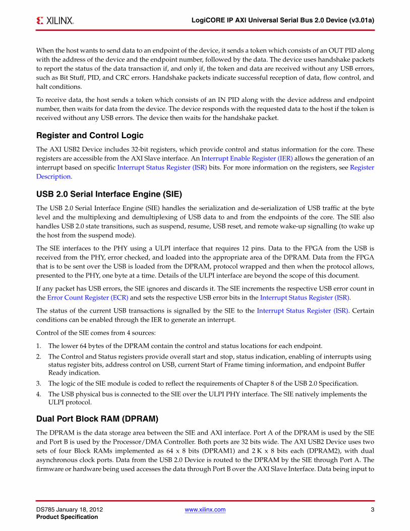
Functional DescriptionThe USB 2.0 protocol multiplexes many devices over a single, half-duplex, serial bus. The bus runs at 480 Mb/s(High Speed) or at 12 Mb/s (Full Speed) and is designed to be plug-and-play. The host always controls the bus andsends tokens to each device specifying the required action. Each device has an address on the USB 2.0 bus and hasone or more endpoints that are sources or sinks of data. All devices have the system control endpoint (endpoint 0).
The AXI USB2 Device has eight endpoints, one control endpoint (endpoint 0) and seven user endpoints. Endpoint0 of the USB 2.0 Device has different requirements to the seven user endpoints. Endpoint 0 handles controltransactions only, which start with an 8-byte setup packet and are then followed by zero or more data packets. Thesetup packet is always stored in a dedicated location in the Dual Port Random Access Memory (DPRAM) at anaddress offset of 0x80. When a setup packet is received, the SETUPPkt bit of the Interrupt Status Register (ISR) isset. Data packets are a maximum of 64 bytes. These data packets are stored in a single bidirectional data buffer setup by the configuration memory of Endpoint 0, located at the address offset 0x0 in the DPRAM. When a datapacket is transmitted or received successfully, the FIFOBufFree and FIFOBufRdy bits of the Interrupt StatusRegister (ISR) are set respectively.
The seven user endpoints of the AXI USB2 Device can be configured as bulk, interrupt or isochronous. In addition,endpoints can be configured as INPUT (to the host) or OUTPUT (from the host). Each of these endpoints has twoping-pong buffers of the same size for endpoint data. The user endpoints data buffers are unidirectional, and areconfigured by the Endpoint Configuration and Status register of the respective endpoint. The size of the buffers canbe configured from 0 to 512 bytes for bulk, 64 bytes for interrupt, and up to 1024 bytes for isochronous endpoints.
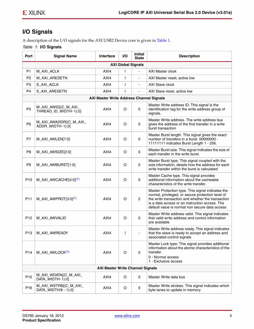
The AXI USB 2.0 High Speed Device core with the AXI and ULPI interfaces is shown in Figure 1 and described inthe subsequent sections.
X-Ref Target - Figure 1
Figure 1: AXI USB2 Device with AXI and ULPI Interfaces
AXIMaster
Interface
AXISlave
Interface
DMAController
USB 2.0SIE
ULPIPHY
AXI USB2 Device
DPRAM 2
Por
t A
Por
t B
32-bit
DPRAM 1
Por
t A
Por
t B
32-bit
Register andControl Logic
32-bit
32-bit
32-bit
32-bit
32-bit
8-bitULPI
Interface
USBBus
32-bitAXI
Interface
DS785_01
Notes:1. The DMA Controller and the AXI Master Interface Module will be included if the parameter C_INCLUDE_DMA=1.2. Enabling DMA logic disconnects the AXI slave interface from DPRAM2.
See Note 1.
See Note 2.
DS785 January 18, 2012 www.xilinx.com 3Product Specification
LogiCORE IP AXI Universal Serial Bus 2.0 Device (v3.01a)
When the host wants to send data to an endpoint of the device, it sends a token which consists of an OUT PID alongwith the address of the device and the endpoint number, followed by the data. The device uses handshake packetsto report the status of the data transaction if, and only if, the token and data are received without any USB errors,such as Bit Stuff, PID, and CRC errors. Handshake packets indicate successful reception of data, flow control, andhalt conditions.
To receive data, the host sends a token which consists of an IN PID along with the device address and endpointnumber, then waits for data from the device. The device responds with the requested data to the host if the token isreceived without any USB errors. The device then waits for the handshake packet.
Register and Control Logic
The AXI USB2 Device includes 32-bit registers, which provide control and status information for the core. Theseregisters are accessible from the AXI Slave interface. An Interrupt Enable Register (IER) allows the generation of aninterrupt based on specific Interrupt Status Register (ISR) bits. For more information on the registers, see RegisterDescription.
USB 2.0 Serial Interface Engine (SIE)
The USB 2.0 Serial Interface Engine (SIE) handles the serialization and de-serialization of USB traffic at the bytelevel and the multiplexing and demultiplexing of USB data to and from the endpoints of the core. The SIE alsohandles USB 2.0 state transitions, such as suspend, resume, USB reset, and remote wake-up signalling (to wake upthe host from the suspend mode).
The SIE interfaces to the PHY using a ULPI interface that requires 12 pins. Data to the FPGA from the USB isreceived from the PHY, error checked, and loaded into the appropriate area of the DPRAM. Data from the FPGAthat is to be sent over the USB is loaded from the DPRAM, protocol wrapped and then when the protocol allows,presented to the PHY, one byte at a time. Details of the ULPI interface are beyond the scope of this document.
If any packet has USB errors, the SIE ignores and discards it. The SIE increments the respective USB error count inthe Error Count Register (ECR) and sets the respective USB error bits in the Interrupt Status Register (ISR).
The status of the current USB transactions is signalled by the SIE to the Interrupt Status Register (ISR). Certainconditions can be enabled through the IER to generate an interrupt.
Control of the SIE comes from 4 sources:
1. The lower 64 bytes of the DPRAM contain the control and status locations for each endpoint.
2. The Control and Status registers provide overall start and stop, status indication, enabling of interrupts using status register bits, address control on USB, current Start of Frame timing information, and endpoint Buffer Ready indication.
3. The logic of the SIE module is coded to reflect the requirements of Chapter 8 of the USB 2.0 Specification.
4. The USB physical bus is connected to the SIE over the ULPI PHY interface. The SIE natively implements the ULPI protocol.
Dual Port Block RAM (DPRAM)
The DPRAM is the data storage area between the SIE and AXI interface. Port A of the DPRAM is used by the SIEand Port B is used by the Processor/DMA Controller. Both ports are 32 bits wide. The AXI USB2 Device uses twosets of four Block RAMs implemented as 64 x 8 bits (DPRAM1) and 2 K x 8 bits each (DPRAM2), with dualasynchronous clock ports. Data from the USB 2.0 Device is routed to the DPRAM by the SIE through Port A. Thefirmware or hardware being used accesses the data through Port B over the AXI Slave Interface. Data being input to
DS785 January 18, 2012 www.xilinx.com 4Product Specification
LogiCORE IP AXI Universal Serial Bus 2.0 Device (v3.01a)
the AXI USB2 Device is loaded through the AXI Slave Interface to Port B, into appropriate locations in the DPRAM.When the host requests data from the device, the SIE accesses this data from Port A.
The DPRAM is seen by the SIE as DPRAM1 and DPRAM2. DPRAM2 has seven endpoint FIFOs for endpoint 1-7.DPRAM1 has the endpoint 0 FIFO and the control register area which defines how the memory is arranged andreports the status of each FIFO buffer (ready, not ready or count). Each FIFO is double buffered to help support thehigh throughput possible with USB 2.0. One buffer can be used for a current USB transaction, while the other bufferis available to the user application for processing. The SIE treats the storage area as FIFOs. The firmware orhardware can access the storage as ordinary RAM over the AXI Slave Interface.
AXI Slave Interface
The AXI Slave interface in the core performs the following operations:
• Responds to AXI transactions to read from or write to the 32-bit control registers, status registers, and DPRAM.
• Supports byte, half word, and word transfers for the DPRAM, but only word transfers are supported for the registers.
AXI Master Interface
The AXI Master interface in the core performs the following operations:
• Performs read and write transactions as a AXI master in DMA mode.
• In DMA mode, interrupts are generated based on DMA Done and DMA Error conditions.
DMA Controller
The Direct Memory Access (DMA) controller is included in the AXI USB2 Device core if the C_INCLUDE_DMAparameter is set to 1. The DMA controller provides simple Direct Memory Access services between DPRAM2 andan external memory device or peripheral on the AXI interface. The DMA controller transfers data from a sourceaddress to a destination address without processor intervention for a given length. It provides programmableregisters (for both directions read from and write to DPRAM2), source address, destination address, and transferlength. The source and destination address counters are increment-only. It also supports AXI burst transfers. TheDMA controller in the core performs data transfers between DPRAM2K and external memory only.
In a DMA transfer the DPRAM2 address should always be an aligned address. A user configurable parameterC_DMA_UA_TRANS_SUPPORT is defined to configure the support of un-aligned external memory addresses.When the parameter C_DMA_UA_TRANS_SUPPORT is set to 1, the DMA controller takes care of the datare-alignment and the DMA source or destination registers can be un-aligned addresses depending on the directionbit in the DMA control register. When C_DMA_UA_TRANS_SUPPORT is set to 0, the DMA controller supportsonly aligned addresses.
ULPI PHY
The USB PHY can be any ULPI compliant PHY. The primary function of the PHY is to manage the bit levelserialization and de-serialization of USB 2.0 traffic. To do so, it must detect and recover the USB clock. The clockruns at 480 MHz, a speed that is too fast for practical implementation on the FPGA. Because 480 MHz is also too fastfor the USB SIE clock, the PHY interfaces to the SIE on a byte serial basis and generates a 60 MHz clock which runson the SIE side of the USB 2.0 Device.
DS785 January 18, 2012 www.xilinx.com 5Product Specification
LogiCORE IP AXI Universal Serial Bus 2.0 Device (v3.01a)
I/O SignalsA description of the I/O signals for the AXI USB2 Device core is given in Table 1.
Table 1: I/O Signals
Port Signal Name Interface I/O InitialState Description
AXI Global Signals
P1 M_AXI_ACLK AXI4 I - AXI Master clock
P2 M_AXI_ARESETN AXI4 I - AXI Master reset, active low
P3 S_AXI_ACLK AXI4 I - AXI Slave clock
P4 S_AXI_ARESETN AXI4 I - AXI Slave reset, active low
AXI Master Write Address Channel Signals
P5 M_AXI_AWID[(C_M_AXI_THREAD_ID_WIDTH-1):0] AXI4 O 0
Master Write address ID. This signal is the identification tag for the write address group of signals.
P6 M_AXI_AWADDR[(C_M_AXI_ADDR_WIDTH-1):0] AXI4 O 0
Master Write address. The write address bus gives the address of the first transfer in a write burst transaction
P7 M_AXI_AWLEN[7:0] AXI4 O 0Master Burst length. This signal gives the exact number of transfers in a burst. 00000000 - 11111111 indicates Burst Length 1 - 256.
P8 M_AXI_AWSIZE[2:0] AXI4 O 0 Master Burst size. This signal indicates the size of each transfer in the write burst.
P9 M_AXI_AWBURST[1:0] AXI4 O 0Master Burst type. This signal coupled with the size information, details how the address for each write transfer within the burst is calculated
P10 M_AXI_AWCACHE[4:0](1) AXI4 O 0Master Cache type. This signal provides additional information about the cacheable characteristics of the write transfer.
P11 M_AXI_AWPROT[3:0](1) AXI4 O 2
Master Protection type. This signal indicates the normal, privileged, or secure protection level of the write transaction and whether the transaction is a data access or an instruction access. The default value is normal non secure data access
P12 M_AXI_AWVALID AXI4 O 0Master Write address valid. This signal indicates that valid write address and control information are available
P13 M_AXI_AWREADY AXI4 I -Master Write address ready. This signal indicates that the slave is ready to accept an address and associated control signals
P14 M_AXI_AWLOCK(1) AXI4 O 0
Master Lock type: This signal provides additional information about the atomic characteristics of the transfer.0 - Normal access1 - Exclusive access
AXI Master Write Channel Signals
P15 M_AXI_WDATA[(C_M_AXI_DATA_WIDTH-1):0] AXI4 O 0 Master Write data bus
P16 M_AXI_WSTRB[(C_M_AXI_DATA_WIDTH/8 - 1):0] AXI4 O 0 Master Write strobes. This signal indicates which
byte lanes to update in memory
DS785 January 18, 2012 www.xilinx.com 6Product Specification
LogiCORE IP AXI Universal Serial Bus 2.0 Device (v3.01a)
P17 M_AXI_WLAST AXI4 O 0 Master Write last. This signal indicates the last transfer in a write burst
P18 M_AXI_WVALID AXI4 O 0 Master Write valid. This signal indicates that valid write data and strobes are available
P19 M_AXI_WREADY AXI4 I - Master Write ready. This signal indicates that the slave can accept the write data
AXI Master Write Response Channel Signals
P20 M_AXI_BID[(C_M_AXI_THREAD_ID_WIDTH-1):0] AXI4 I -
Master Write response ID. This signal is the identification tag of the write response. The BID value must match the AWID value of the write transaction to which the slave is responding
P21 M_AXI_BRESP[1:0] AXI4 I - Master Write response. This signal indicates the status of the write transaction
P22 M_AXI_BVALID AXI4 I - Master Write response valid. This signal indicates that a valid write response is available
P23 M_AXI_BREADY AXI4 O - Master Response ready. This signal indicates that the master can accept the response information
AXI Master Read Address Channel Signals
P24 M_AXI_ARID[(C_M_AXI_THREAD_ID_WIDTH-1):0] AXI4 O 0
Master Read address ID. This signal is the identification tag for the read address group of signals
P25 M_AXI_ARADDR[(C_M_AXI_ADDR_WIDTH-1):0] AXI4 O 0 Master Read address. The read address bus
gives the initial address of a read burst transaction
P26 M_AXI_ARLEN[7:0] AXI4 O 0Master Burst length. This signal gives the exact number of transfers in a burst. 00000000 - 11111111 indicates Burst Length 1 - 256.
P27 M_AXI_ARSIZE[2:0] AXI4 O 0 Master Burst size. This signal indicates the size of each transfer in the read burst.
P28 M_AXI_ARBURST[1:0] AXI4 O 0Master Burst type. The burst type, coupled with the size information, details how the address for each read transfer within the burst is calculated.
P29 M_AXI_ARCACHE[4:0](1) AXI4 O 0Master Cache type. This signal provides additional information about the cacheable characteristics of the read transfer.
P30 M_AXI_ARPROT[3:0](1) AXI4 O 2
Master Protection type. This signal provides protection unit information for the read transaction. The default value is normal non secure data access
P31 M_AXI_ARVALID AXI4 O 0
Master Read address valid. This signal indicates, when high, that the read address and control information is valid and remains stable until the address acknowledgement signal, ARREDY, is high.
P32 M_AXI_ARREADY AXI4 I -Master Read address ready. This signal indicates that the slave is ready to accept an address and associated control signals.
Table 1: I/O Signals (Cont’d)
Port Signal Name Interface I/O InitialState Description
DS785 January 18, 2012 www.xilinx.com 7Product Specification
LogiCORE IP AXI Universal Serial Bus 2.0 Device (v3.01a)
P33 M_AXI_ARLOCK(1) AXI4 O 0
Master Lock type: This signal provides additional information about the atomic characteristics of the transfer.0 - Normal access1 - Exclusive access
AXI Master Read Data Channel Signals
P34 M_AXI_RID[(C_M_AXI_THREAD_ID_WIDTH-1):0] AXI4 I -
Master Read ID tag. This signal is the ID tag of the read data group of signals. The RID value is generated by the slave and must match the ARID value of the read transaction to which it is responding.
P35 M_AXI_RDATA[(C_M_AXI_DATA_WIDTH-1):0] AXI4 I - Master Read data bus
P36 M_AXI_RRESP[1:0] AXI4 I - Master Read response. This signal indicates the status of the read transfer.
P37 M_AXI_RLAST AXI4 I - Master Read last. This signal indicates the last transfer in a read burst
P38 M_AXI_RVALID AXI4 I -Master Read valid. This signal indicates that the required read data is available and the read transfer can complete
P39 M_AXI_RREADY AXI4 O 0Master Read ready. This signal indicates that the master can accept the read data and response information
AXI Slave Write Address Channel Signals
P40 S_AXI_AWID[(C_S_AXI_ID_WIDTH-1):0] AXI4 I -
Slave Write address ID: This signal is the identification tag for the write address group of signals.
P41 S_AXI_AWADDR[(C_S_AXI_ADDR_WIDTH-1):0] AXI4 I -
Slave Write address: The write address bus gives the address of the first transfer in a write burst transaction.
P42 S_AXI_AWLEN[7:0] AXI4 I -Slave Burst length: This signal gives the exact number of transfers in a burst. 00000000 - 11111111 indicates Burst Length 1 - 256.
P43 S_AXI_AWSIZE[2:0] AXI4 I -
Slave Burst size: This signal indicates the size of each transfer in the burst.000 - 1 byte001 - 2 byte (half word)010 - 4 byte (word)011 - 8 byte (double word)others - NA
P44 S_AXI_AWBURST[1:0] AXI4 I -
Slave Burst type: This signal coupled with the size information, details how the address for each transfer within the burst is calculated.00 - FIXED01 - INCR10 - WRAP11 - Reserved
Table 1: I/O Signals (Cont’d)
Port Signal Name Interface I/O InitialState Description
DS785 January 18, 2012 www.xilinx.com 8Product Specification
LogiCORE IP AXI Universal Serial Bus 2.0 Device (v3.01a)
P45 S_AXI_AWLOCK(1) AXI4 I -
Slave Lock type: This signal provides additional information about the atomic characteristics of the transfer.0 - Normal access1 - Exclusive access
P46 S_AXI_AWCACHE[3:0](1) AXI4 I -
Slave Cache type: This signal indicates the bufferable, cacheable, write-through, write-back and allocate attributes of the transactionBit-0 : Bufferable (B)Bit-1 : Cacheable (C)Bit-2 : Read Allocate (RA)Bit-3 : Write Allocate (WA)The combination where C=0 and WA/RA=1 are reserved.
P47 S_AXI_AWPROT[2:0](1) AXI4 I -
Slave Protection type: This signal indicates the normal, privileged, or secure protection level of the transaction and whether the transaction is a data access or an instruction access.Bit-0 : 0=Normal access, 1=Privileged accessBit-1 : 0=Secure access, 1=Non-secure accessBit-2 : 0=Data access; 1=Instruction access
P48 S_AXI_AWVALID AXI4 I -Slave Write address valid: This signal indicates that valid write address and control information are available.
P49 S_AXI_AWREADY AXI4 O 0Slave Write address ready: This signal indicates that the slave is ready to accept an address and associated control signals.
AXI Slave Write Channel Signals
P50 S_AXI_WDATA[(C_S_AXI_DATA_WIDTH-1):0] AXI4 I - Slave Write data bus.
P51 S_AXI_WSTRB[((C_S_AXI_DATA_WIDTH/8) - 1):0] AXI4 I - Slave Write strobes: This signal indicates which
byte lanes in S_AXI_WDATA are valid.
P52 S_AXI_WLAST AXI4 I - Slave Write last: This signal indicates the last transfer in a write burst.
P53 S_AXI_WVALID AXI4 I - Slave Write valid: This signal indicates that valid write data and strobes are available.
P54 S_AXI_WREADY AXI4 O 0 Slave Write ready: This signal indicates that the slave can accept the write data.
AXI Slave Write Response Channel Signals
P55 S_AXI_BID[(C_S_AXI_ID_WIDTH-1):0] AXI4 O 0
Slave Write response ID: This signal is the identification tag of the write response. The BID value must match the AWID value of the write transaction to which the slave is responding.
P56 S_AXI_BRESP[1:0] AXI4 O 0
Slave Write response: This signal indicates the status of the write transaction.00 - OKAY01 - EXOKAY - NA10 - SLVERR11 - DECERR - NA
P57 S_AXI_BVALID AXI4 O 0 Slave Write response valid: This signal indicates that a valid write response is available.
Table 1: I/O Signals (Cont’d)
Port Signal Name Interface I/O InitialState Description
DS785 January 18, 2012 www.xilinx.com 9Product Specification
LogiCORE IP AXI Universal Serial Bus 2.0 Device (v3.01a)
P58 S_AXI_BREADY AXI4 I - Slave Response ready: This signal indicates that the master can accept the response information.
AXI Slave Read Address Channel Signals
P59 S_AXI_ARID[(C_S_AXI_ID_WIDTH-1):0] AXI4 I -
Slave Read address ID: This signal is the identification tag for the read address group of signals.
P60 S_AXI_ARADDR[(C_S_AXI_ADDR_WIDTH-1):0] AXI4 I - Slave Read address: The read address bus gives
the initial address of a read burst transaction.
P61 S_AXI_ARLEN[7:0] AXI4 I -Slave Burst length: This signal gives the exact number of transfers in a burst. 00000000 - 11111111 indicates Burst Length 1 - 256.
P62 S_AXI_ARSIZE[2:0] AXI4 I -
Slave Burst size: This signal indicates the size of each transfer in the burst.000 - 1 byte001 - 2 byte (Half word)010 - 4 byte (word)011 - 8 byte (double word)others - NA
P63 S_AXI_ARBURST[1:0] AXI4 I -
Slave Burst type: The burst type, coupled with the size information, details how the address for each transfer within the burst is calculated.00 - FIXED01 - INCR10 - WRAP11 - Reserved
P64 S_AXI_ARLOCK(1) AXI4 I -
Slave Lock type: This signal provides additional information about the atomic characteristics of the transfer.0 - Normal access1 - Exclusive access
P65 S_AXI_ARCACHE[3:0](1) AXI4 I -
Slave Cache type: This signal provides additional information about the cacheable characteristics of the transfer.Bit-0 : Bufferable (B)Bit-1 : Cacheable (C)Bit-2 : Read Allocate (RA)Bit-3 : Write Allocate (WA)The combination where C=0 and WA/RA=1 are reserved.
P66 S_AXI_ARPROT[2:0](1) AXI4 I - Slave Protection type: This signal provides protection unit information for the transaction.
P67 S_AXI_ARVALID AXI4 I -
Slave Read address valid: This signal indicates, when high, that the read address and control information is valid and remains stable until the address acknowledgement signal, S_AXI_ARREADY, is high.
P68 S_AXI_ARREADY AXI4 O 0Slave Read address ready: This signal indicates that the slave is ready to accept an address and associated control signals.
Table 1: I/O Signals (Cont’d)
Port Signal Name Interface I/O InitialState Description
DS785 January 18, 2012 www.xilinx.com 10Product Specification
LogiCORE IP AXI Universal Serial Bus 2.0 Device (v3.01a)
AXI Slave Read Data Channel Signals
P69 S_AXI_RID[(C_S_AXI_ID_WIDTH-1):0] AXI4 O 0
Slave Read ID tag: This signal is the ID tag of the read data group of signals. The S_AXI_RID value is generated by the slave and must match the ARID value of the read transaction to which it is responding.
P70 S_AXI_RDATA[(C_S_AXI_DATA_WIDTH-1):0] AXI4 O 0 Slave Read data bus.
P71 S_AXI_RRESP[1:0] AXI4 O 0
Slave Read response: This signal indicates the status of the read transfer.00 - OKAY01 - EXOKAY - NA10 - SLVERR11 - DECERR - NA
P72 S_AXI_RLAST AXI4 O 0 Slave Read last: This signal indicates the last transfer in a read burst.
P73 S_AXI_RVALID AXI4 O 0Slave Read valid: This signal indicates that the required read data is available and the read transfer can complete.
P74 S_AXI_RREADY AXI4 I -Slave Read ready: This signal indicates that the master can accept the read data and response information.
System Signals
P75 USB_Irpt System O 0 USB Interrupt
USB Specific Signals
P76 ULPI_Clock USB I - All USB protocol interface signals are synchronous to this clock
P77 ULPI_Dir USB I - Direction of data flow between the PHY and SIE
P78 ULPI_Next USB I - Indicator of when the PHY is ready for the next bit
P79 ULPI_Stop USB O 0 Indicator that transmission of last byte is complete
P80 ULPI_Reset(2) USB O 1 Reset to the ULPI PHY
P81 ULPI_Data_I(7:0) USB I - Input data from the PHY to the SIE
P82 ULPI_Data_O(7:0) USB O 0 Output data from the SIE to the PHY
P83 ULPI_Data_T USB O 0ULPI_Data is a 3-state port with ULPI_Data_I as the IN port, ULPI_Data_O as the OUT port and ULPI_Data_T as the 3-state output
Optional Ports Used for Debug Purpose
P84 Configured USB O 0 Used for USB2.0 Certification - Test mode NAK
P85 Spare1 USB O 0 Used for USB2.0 Certification -Test mode J
P86 Spare2 USB O 0 Used for USB2.0 Certification - Test mode K
P87 Vbus_detect USB O 0 0 = Indicates valid VBUS has not been detected1 = Indicates Valid VBUS has been detected
P88 Show_currentspeed USB O 0 0 = indicates Full Speed1 = indicates High Speed
Table 1: I/O Signals (Cont’d)
Port Signal Name Interface I/O InitialState Description
DS785 January 18, 2012 www.xilinx.com 11Product Specification
LogiCORE IP AXI Universal Serial Bus 2.0 Device (v3.01a)
Design ParametersTo obtain an AXI USB2 Device that is uniquely tailored to the system requirements, certain features can beparameterized in the AXI USB2 Device design. The features that can be parameterized in the Xilinx AXI USB2Device design are shown in Table 2.
Inferred Parameters
In addition to the parameters listed in Table 2, there are also parameters that are inferred for each AXI interface inthe EDK tools. Through the design, these EDK-inferred parameters control the behavior of the AXI Interconnect.For a complete list of the interconnect settings related to the AXI interface, see [Ref 4].
P89 Running USB O 0
0 = indicates that the SIE is in reset state and does not respond to USB traffic1= indicates that the SIE is finished USB reset and is ready to respond to USB traffic
P90 Suspended USB O 0
0 = Indicates AXI USB2 Device has been suspended1 = Indicates AXI USB2 Device has not been suspended
P91 Disconnected USB O 0 0 = Indicates AXI USB2 Device is connected1 = Indicates AXI USB2 Device is disconnected
Notes: 1. This signal has no significance in the design; if the signal is an input it is not used; outputs are hard-coded to default values.2. The polarity of the ULPI reset port is user-configurable. The C_PHY_RESET_TYPE parameter defines the type of the ULPI reset
as either active high or active low.
Table 2: Design Parameters
Generic Feature/Description Parameter Name Allowable
ValuesReset Value VHDL Type
System Parameter
G1 Device family C_FAMILY spartan6, virtex6, 7 series, zynq virtex6 string
G2 AXI USB2 Device Base Address C_BASEADDR Valid Address(1),(2) None std_logic_vector
G3 AXI USB2 Device High Address C_HIGHADDR Valid Address(1),(2) None std_logic_vector
AXI4 Master Interface Parameters
G4 AXI Master address bus width C_M_AXI_ADDR_WIDTH 32 32 integer
G5 AXI Master data bus width C_M_AXI_DATA_WIDTH 32 32 integer
G6 AXI Master Identification tag width C_M_AXI_THREAD_ID_WIDTH 1-2 1 integer
AXI4 Slave Interface Parameters
G7 AXI Slave address bus width C_S_AXI_ADDR_WIDTH 32 32 integer
G8 AXI Slave data bus width C_S_AXI_DATA_WIDTH 32 32 integer
G9 AXI Slave Identification tag width C_S_AXI_ID_WIDTH 1- 16 4 integer
Table 1: I/O Signals (Cont’d)
Port Signal Name Interface I/O InitialState Description
DS785 January 18, 2012 www.xilinx.com 12Product Specification
LogiCORE IP AXI Universal Serial Bus 2.0 Device (v3.01a)
Allowable Parameter Combinations The address-range size specified by C_BASEADDR and C_HIGHADDR must be a power of 2, and must be at least0x7FFF. For example, if C_BASEADDR = 0x80000000, C_HIGHADDR must be at least = 0x80007FFF.
Parameter - Port DependenciesThe width of some of the AXI USB2 Device signals depends on parameters selected in the design. The dependenciesbetween the AXI USB2 Device design parameters and I/O signals are shown in Table 3.
USB2.0 Core Specific Parameters
G10 Implementation of DMA C_INCLUDE_DMA 0-1(3) 1 integer
G11 Type of ULPI PHY reset C_PHY_RESET_TYPE 0-1(4) 1 integer
G12 Enables USB error counters C_INCLUDE_USBERR_LOGIC 0-1(5) 0 integer
G13 Select Buffer typeon ULPI Clock
C_ULPI_CLK_BUFFER_TYPE
IBUFG/IBUF/BUFG/BUFR/NONE(6) IBUFG string
G14
Support for un-aligned transactions on DMA. This parameter is valid only when C_INCLUDE_DMA is set.
C_DMA_UA_TRANS_SUPPORT 0-1(7) 0 integer
Notes: 1. Address range specified by C_BASEADDR and C_HIGHADDR must be at least 0x8000 and must be power of 2. C_BASEADDR
must be multiple of the range, where the range is C_HIGHADDR - C_BASEADDR + 12. No default value is specified to ensure that the actual value is set; that is, if the value is not set, a compiler error is generated. The
address range must be at least 0x7FFF. For example, C_BASEADDR = 0x80000000, C_HIGHADDR = 0x80007FFF.3. If C_INCLUDE_DMA = 1, the DMA controller logic is included in the core. The RAM can be accessed for endpoint 1-7 buffers
through the DMA controller only; enabling the DMA logic disconnects the AXI slave interface from endpoint 1-7 buffers.4. If C_PHY_RESET_TYPE = 1, the core puts an active high reset condition on the ULPI reset port. Otherwise the core drives an
active low hard reset condition.5. If C_INCLUDE_USBERR_LOGIC = 1, USB ERROR interrupt generation logic is included; otherwise the core excludes the USB
ERROR interrupt generation logic from the core. This parameter is added to reduce the resources used for the generation of USB ERROR interrupt and the respective counters from the core
6. The buffer type on the ULPI clock port can be selected by configuring the C_ULPI_CLK_BUFFGER_TYPE parameter.7. If C_DMA_UA_TRANS_SUPPORT = 1, the DMA controller supports un-aligned addresses. If this parameter is set to ‘0’, the DMA
controller does not support un-aligned transactions. The aligned addresses for DMA transactions must be sent.
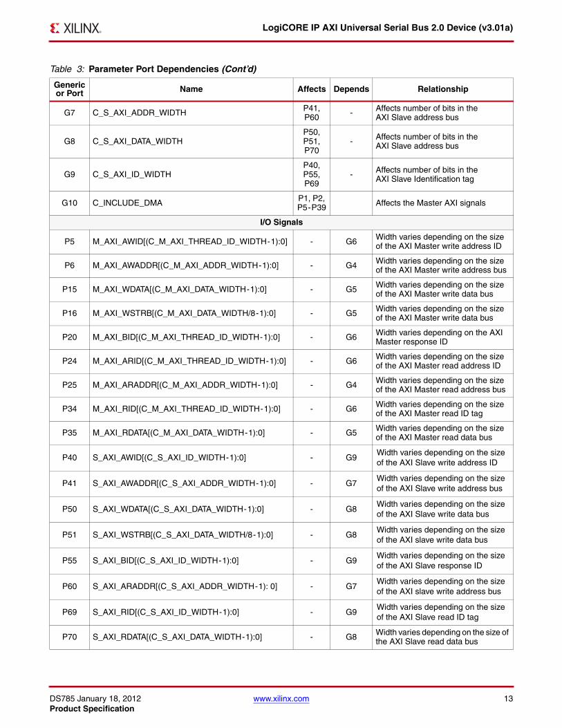
Table 3: Parameter Port Dependencies
Genericor Port Name Affects Depends Relationship
Design Parameters
G4 C_M_AXI_ADDR_WIDTH P6, P25 - Affects number of bits in the AXI Master address bus
G5 C_M_AXI_DATA_WIDTHP15, P16, P35
- Affects number of bits in the AXI Master data bus
G6 C_M_AXI_THREAD_ID_WIDTH
P5, P20, P24, P34
- Affects number of bits in the AXI Master Identification tag
Table 2: Design Parameters (Cont’d)
DS785 January 18, 2012 www.xilinx.com 13Product Specification
LogiCORE IP AXI Universal Serial Bus 2.0 Device (v3.01a)
G7 C_S_AXI_ADDR_WIDTH P41, P60 - Affects number of bits in the
AXI Slave address bus
G8 C_S_AXI_DATA_WIDTHP50, P51, P70
- Affects number of bits in theAXI Slave address bus
G9 C_S_AXI_ID_WIDTHP40, P55, P69
- Affects number of bits in theAXI Slave Identification tag
G10 C_INCLUDE_DMA P1, P2, P5-P39 Affects the Master AXI signals
I/O Signals
P5 M_AXI_AWID[(C_M_AXI_THREAD_ID_WIDTH-1):0] - G6 Width varies depending on the sizeof the AXI Master write address ID
P6 M_AXI_AWADDR[(C_M_AXI_ADDR_WIDTH-1):0] - G4 Width varies depending on the sizeof the AXI Master write address bus
P15 M_AXI_WDATA[(C_M_AXI_DATA_WIDTH-1):0] - G5 Width varies depending on the sizeof the AXI Master write data bus
P16 M_AXI_WSTRB[(C_M_AXI_DATA_WIDTH/8-1):0] - G5 Width varies depending on the sizeof the AXI Master write data bus
P20 M_AXI_BID[(C_M_AXI_THREAD_ID_WIDTH-1):0] - G6 Width varies depending on the AXIMaster response ID
P24 M_AXI_ARID[(C_M_AXI_THREAD_ID_WIDTH-1):0] - G6 Width varies depending on the sizeof the AXI Master read address ID
P25 M_AXI_ARADDR[(C_M_AXI_ADDR_WIDTH-1):0] - G4 Width varies depending on the sizeof the AXI Master read address bus
P34 M_AXI_RID[(C_M_AXI_THREAD_ID_WIDTH-1):0] - G6 Width varies depending on the sizeof the AXI Master read ID tag
P35 M_AXI_RDATA[(C_M_AXI_DATA_WIDTH-1):0] - G5 Width varies depending on the sizeof the AXI Master read data bus
P40 S_AXI_AWID[(C_S_AXI_ID_WIDTH-1):0] - G9Width varies depending on the sizeof the AXI Slave write address ID
P41 S_AXI_AWADDR[(C_S_AXI_ADDR_WIDTH-1):0] - G7Width varies depending on the sizeof the AXI Slave write address bus
P50 S_AXI_WDATA[(C_S_AXI_DATA_WIDTH-1):0] - G8Width varies depending on the sizeof the AXI Slave write data bus
P51 S_AXI_WSTRB[(C_S_AXI_DATA_WIDTH/8-1):0] - G8Width varies depending on the sizeof the AXI slave write data bus
P55 S_AXI_BID[(C_S_AXI_ID_WIDTH-1):0] - G9Width varies depending on the sizeof the AXI Slave response ID
P60 S_AXI_ARADDR[(C_S_AXI_ADDR_WIDTH-1): 0] - G7Width varies depending on the size of the AXI slave write address bus
P69 S_AXI_RID[(C_S_AXI_ID_WIDTH-1):0] - G9Width varies depending on the size of the AXI Slave read ID tag
P70 S_AXI_RDATA[(C_S_AXI_DATA_WIDTH-1):0] - G8 Width varies depending on the size of the AXI Slave read data bus
Table 3: Parameter Port Dependencies (Cont’d)
Genericor Port Name Affects Depends Relationship
DS785 January 18, 2012 www.xilinx.com 14Product Specification
LogiCORE IP AXI Universal Serial Bus 2.0 Device (v3.01a)
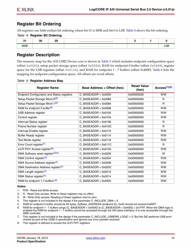
Register Bit OrderingAll registers use little-endian bit ordering where bit-31 is MSB and bit-0 is LSB. Table 4 shows the bit ordering.
Register DescriptionThe memory map for the AXI USB2 Device core is shown in Table 5 which includes endpoint configuration space(offset 0x0000), setup packet storage space (offset 0x0080), RAM for endpoint 0 buffer (offset 0x0088), registerspace for the USB registers (offset 0x0100), and RAM for endpoint 1 - 7 buffers (offset 0x4000). Table 6 lists themapping for endpoint configuration space. All offsets are word offsets.
Table 4: Register Bit Ordering
31 30 29 . . . . . . . . . . . . . . . . . . . . . . 2 1 0
MSB . . . . . . . . . . . . . . . . . . . . . . LSB
Table 5: Register Address Map
Register Name Base Address + Offset (hex)Reset Value
(hex)Access(1)(2)
Endpoint Configuration and Status registers C_BASEADDR + 0x0000 0x00000000 R/W
Setup Packet Storage Word 0(2) C_BASEADDR + 0x0080 0x00000000 R
Setup Packet Storage Word 1(2) C_BASEADDR + 0x0084 0x00000000 R
RAM for endpoint 0 buffer(6) C_BASEADDR + 0x0088 0x00000000 R/W
USB Address register C_BASEADDR + 0x0100 0x00000000 R/W
Control register C_BASEADDR + 0x0104 0x00000000 R/W
Interrupt Status register C_BASEADDR + 0x0108 0x00000000 R
Frame Number register C_BASEADDR + 0x010C 0x00000000 R
Interrupt Enable register C_BASEADDR + 0x0110 0x00000000 R/W
Buffer Ready register C_BASEADDR + 0x0114 0x00000000 R/W
Test Mode register C_BASEADDR + 0x0118 0x00000000 R/W
Error Count register(7) C_BASEADDR + 0x011C 0x00000000 R
ULPI PHY Access register(8) C_BASEADDR + 0x0120 0x00000000 R/W
DMA Software reset register(3)(4) C_BASEADDR + 0x0200 0x00000000 W
DMA Control register(4) C_BASEADDR + 0x0204 0x00000000 R/W
DMA Source Address register(4) C_BASEADDR + 0x0208 0x00000000 R/W
DMA Destination Address register(4) C_BASEADDR + 0x020C 0x00000000 R/W
DMA Length register(4) C_BASEADDR + 0x0210 0x00000000 R/W
DMA Status register(4) C_BASEADDR + 0x0214 0x00000000 R/W
RAM for endpoint 1-7 buffers (6) C_BASEADDR + 0x4000 0x00000000 R/W
Notes: 1. R/W - Read and Write access2. R - Read Only access. Write to these registers has no effect3. W - Write Only access. Reading of these registers returns zero4. This register is not included in the design if the parameter C_INCLUDE_DMA = 05. RAM for endpoint 0 buffer should be 64 bytes, EpBase_ADDRESS (endpoint 0)+ 0x40 should not exceed 0x00FF6. RAM for endpoint 1 - 7 buffers range (C_BASEADDR + 0x4000) to (C_BASEADDR + 0x4000) + 0x1FFF. When the DMA logic is
enabled the RAM for endpoint 1 - 7 buffers cannot be accessed through the AXI slave interface; It is only accessible through the DMA controller.
7. This register is not included in the design if the parameter C_INCLUDE_USBERR_LOGIC = 0. But the SIE performs USB error checks as part of the USB2.0 specification and ignores any error packets received.
8. This register is defined to access the ULPI PHY registers.
DS785 January 18, 2012 www.xilinx.com 15Product Specification
LogiCORE IP AXI Universal Serial Bus 2.0 Device (v3.01a)
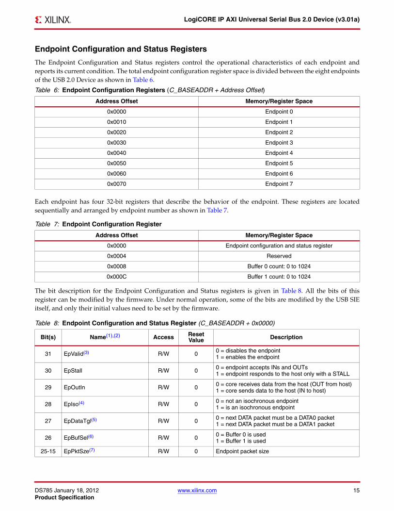
Endpoint Configuration and Status Registers
The Endpoint Configuration and Status registers control the operational characteristics of each endpoint andreports its current condition. The total endpoint configuration register space is divided between the eight endpointsof the USB 2.0 Device as shown in Table 6.
Each endpoint has four 32-bit registers that describe the behavior of the endpoint. These registers are locatedsequentially and arranged by endpoint number as shown in Table 7.
The bit description for the Endpoint Configuration and Status registers is given in Table 8. All the bits of thisregister can be modified by the firmware. Under normal operation, some of the bits are modified by the USB SIEitself, and only their initial values need to be set by the firmware.
Table 6: Endpoint Configuration Registers (C_BASEADDR + Address Offset)
Address Offset Memory/Register Space
0x0000 Endpoint 0
0x0010 Endpoint 1
0x0020 Endpoint 2
0x0030 Endpoint 3
0x0040 Endpoint 4
0x0050 Endpoint 5
0x0060 Endpoint 6
0x0070 Endpoint 7
Table 7: Endpoint Configuration Register
Address Offset Memory/Register Space
0x0000 Endpoint configuration and status register
0x0004 Reserved
0x0008 Buffer 0 count: 0 to 1024
0x000C Buffer 1 count: 0 to 1024
Table 8: Endpoint Configuration and Status Register (C_BASEADDR + 0x0000)
Bit(s) Name(1),(2) Access Reset Value Description
31 EpValid(3) R/W 0 0 = disables the endpoint1 = enables the endpoint
30 EpStall R/W 0 0 = endpoint accepts INs and OUTs1 = endpoint responds to the host only with a STALL
29 EpOutIn R/W 0 0 = core receives data from the host (OUT from host)1 = core sends data to the host (IN to host)
28 EpIso(4) R/W 0 0 = not an isochronous endpoint1 = is an isochronous endpoint
27 EpDataTgl(5) R/W 0 0 = next DATA packet must be a DATA0 packet1 = next DATA packet must be a DATA1 packet
26 EpBufSel(6) R/W 0 0 = Buffer 0 is used1 = Buffer 1 is used
25-15 EpPktSze(7) R/W 0 Endpoint packet size
DS785 January 18, 2012 www.xilinx.com 16Product Specification
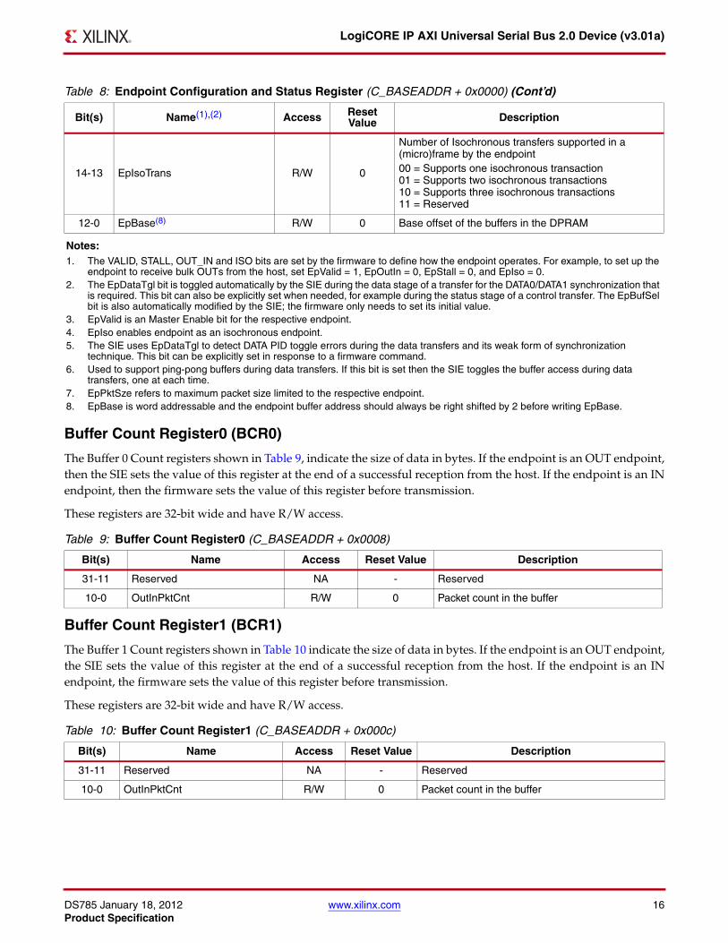
LogiCORE IP AXI Universal Serial Bus 2.0 Device (v3.01a)
Buffer Count Register0 (BCR0)
The Buffer 0 Count registers shown in Table 9, indicate the size of data in bytes. If the endpoint is an OUT endpoint,then the SIE sets the value of this register at the end of a successful reception from the host. If the endpoint is an INendpoint, then the firmware sets the value of this register before transmission.
These registers are 32-bit wide and have R/W access.
Buffer Count Register1 (BCR1)
The Buffer 1 Count registers shown in Table 10 indicate the size of data in bytes. If the endpoint is an OUT endpoint,the SIE sets the value of this register at the end of a successful reception from the host. If the endpoint is an INendpoint, the firmware sets the value of this register before transmission.
These registers are 32-bit wide and have R/W access.
14-13 EpIsoTrans R/W 0
Number of Isochronous transfers supported in a (micro)frame by the endpoint00 = Supports one isochronous transaction01 = Supports two isochronous transactions10 = Supports three isochronous transactions11 = Reserved
12-0 EpBase(8) R/W 0 Base offset of the buffers in the DPRAM
Notes: 1. The VALID, STALL, OUT_IN and ISO bits are set by the firmware to define how the endpoint operates. For example, to set up the
endpoint to receive bulk OUTs from the host, set EpValid = 1, EpOutIn = 0, EpStall = 0, and EpIso = 0.2. The EpDataTgl bit is toggled automatically by the SIE during the data stage of a transfer for the DATA0/DATA1 synchronization that
is required. This bit can also be explicitly set when needed, for example during the status stage of a control transfer. The EpBufSel bit is also automatically modified by the SIE; the firmware only needs to set its initial value.
3. EpValid is an Master Enable bit for the respective endpoint.4. EpIso enables endpoint as an isochronous endpoint.5. The SIE uses EpDataTgl to detect DATA PID toggle errors during the data transfers and its weak form of synchronization
technique. This bit can be explicitly set in response to a firmware command.6. Used to support ping-pong buffers during data transfers. If this bit is set then the SIE toggles the buffer access during data
transfers, one at each time.7. EpPktSze refers to maximum packet size limited to the respective endpoint.8. EpBase is word addressable and the endpoint buffer address should always be right shifted by 2 before writing EpBase.
Table 9: Buffer Count Register0 (C_BASEADDR + 0x0008)
Bit(s) Name Access Reset Value Description
31-11 Reserved NA - Reserved
10-0 OutInPktCnt R/W 0 Packet count in the buffer
Table 10: Buffer Count Register1 (C_BASEADDR + 0x000c)
Bit(s) Name Access Reset Value Description
31-11 Reserved NA - Reserved
10-0 OutInPktCnt R/W 0 Packet count in the buffer
Table 8: Endpoint Configuration and Status Register (C_BASEADDR + 0x0000) (Cont’d)
Bit(s) Name(1),(2) Access Reset Value Description
DS785 January 18, 2012 www.xilinx.com 17Product Specification
LogiCORE IP AXI Universal Serial Bus 2.0 Device (v3.01a)
USB Address Register (UAR)
The USB Address register, shown in Table 11 contains the host-assigned USB address of the device. There are 128possible USB devices on the USB; therefore, the register takes values from 0 to 127. The lower seven bits of theregister (6:0) are used to set the address. An address of 0 indicates that the device is un-enumerated. Address 0 is thedefault address of all USB devices at plug-in time and the address value on hardware reset. This register is 32-bitwide and has R/W access.
Control Register (CR)
As shown in Table 12, the MstRdy bit indicates SIE operation. When clear, the USB SIE is paused and does notrespond to any USB activity. When set, the SIE operates normally. The RmteWkup bit initiates remote wake-upsignalling to the host when the device has been suspended by the host. The core generates USBRsm interrupt afterthe successful completion of remote wake-up signalling with host. The RmteWkup bit remains set until firmwareclears it.
Interrupt Status Register (ISR)
The Interrupt Status Register (ISR) shown in Table 13, reports status on the operation of the AXI USB2 Device core.The bits in this register are cleared as soon as they are read.
Table 11: USB Address Register (C_BASEADDR + 0x0100)
Bit(s) Name Access Reset Value Description
31-7 Reserved NA - Reserved
6-0 USBAddr R/W 0 Indicates the USB address of the device.
Table 12: Control Register (C_BASEADDR + 0x0104)
Bit(s) Name Access Reset Value Description
31 MstRdy R/W 0 0 = SIE is paused and does not respond to any USB activity1 = SIE operates normally
30 RmteWkup R/W 0 0 = SIE does nothing1 = SIE sends remote wake-up signalling to host
29-0 Reserved NA - Reserved
Table 13: Interrupt Status Register (C_BASEADDR + 0x0108)
Bit(s) Name Access Reset Value Description
31 Reserved NA - Reserved
30 ULPIAccComp R 0 0 = ULPI PHY Access Complete has not occurred1 = ULPI PHY Access Complete has occurred
29 BitStufErr(2) R 0 0 = Bit Stuff error has not occurred1 = Bit Stuff error has occurred
28 PidErr(2) R 0 0 = PID error has not occurred1 = PID error has occurred
27 CrcErr(2) R 0 0 = CRC error has not occurred1 = CRC error has occurred
26 DmaDne(1) R 0 0 = DMA operation is not done1 = DMA operation is done
DS785 January 18, 2012 www.xilinx.com 18Product Specification
LogiCORE IP AXI Universal Serial Bus 2.0 Device (v3.01a)
25 DmaErr(1) R 0 0 = DMA error has not occurred1 = DMA error has occurred
24 USBRsm(3) R 0 0 = Core has not received resume signalling from host1 = Core received resume signalling from host
23 USBRst(3) R 0 0 = Core has not received USB reset from host 1 = Core received USB reset from host
22 USBSpnd(3) R 0 0 = Core not in suspend state1 = Core in suspend state
21 USBDsc(3) R 0 0 = Core connected to host1 = Core is disconnected from host
20 FIFOBufRdy R 0 0 = Endpoint 0 packet has not been received by core1 = Endpoint 0 packet has been received by core
19 FIFOBufFree R 0 0 = Endpoint 0 packet has been transmitted by core1 = Endpoint 0 packet has not been transmitted by core
18 SETUPPkt R 0 0 = Endpoint 0 Setup packet has not been received by core1 = Endpoint 0 Setup packet has been received
17 SOFPkt R 0 0 = Start of Frame packet has not been received by core1 = Start of Frame packet has been received by core
16 HighSpd R 00 = Core is running at Full Speed1 = core is running at High Speed
15 Ep7ProcBuf1 R 00 = Endpoint 7, buffer 1 not processed1 = Endpoint 7, buffer 1 processed
14 Ep6ProcBuf1 R 00 = Endpoint 6, buffer 1 not processed1 = Endpoint 6, buffer 1 processed
13 Ep5ProcBuf1 R 00 = Endpoint 5, buffer 1 not processed1 = Endpoint 5, buffer 1 processed
12 Ep4ProcBuf1 R 00 = Endpoint 4, buffer 1 not processed1 = Endpoint 4, buffer 1 processed
11 Ep3ProcBuf1 R 00 = Endpoint 3, buffer 1 not processed1 = Endpoint 3, buffer 1 processed
10 Ep2ProcBuf1 R 00 = Endpoint 2, buffer 1 not processed1 = Endpoint 2, buffer 1 processed
9 Ep1ProcBuf1 R 00 = Endpoint 1, buffer 1 not processed1 = Endpoint 1, buffer 1 processed
8 Reserved NA - Reserved
7 Ep7ProcBuf0 R 00 = Endpoint 7, buffer 0 not processed1 = Endpoint 7, buffer 0 processed
6 Ep6ProcBuf0 R 00 = Endpoint 6, buffer 0 not processed1 = Endpoint 6, buffer 0 processed
5 Ep5ProcBuf0 R 00 = Endpoint 5, buffer 0 not processed1 = Endpoint 5, buffer 0 processed
4 Ep4ProcBuf0 R 00 = Endpoint 4, buffer 0 not processed1 = Endpoint 4, buffer 0 processed
Table 13: Interrupt Status Register (C_BASEADDR + 0x0108) (Cont’d)
Bit(s) Name Access Reset Value Description
DS785 January 18, 2012 www.xilinx.com 19Product Specification
LogiCORE IP AXI Universal Serial Bus 2.0 Device (v3.01a)
The USB 2.0 Device has a single interrupt line (USB_Irpt) to indicate an interrupt. Interrupts are indicated byasserting the USB_Irpt signal (transition of the USB_Irpt from a logic '0' to a logic '1').
The Interrupt Enable Register (IER) allows specific bits of the Interrupt Status Register (ISR) to generate interrupts.The MstEnbl bit of the Interrupt Enable Register (IER) register allows all interrupts to be disabled simultaneously.The interrupt condition is cleared when the corresponding bit of the Interrupt Status Register (ISR) is cleared bywriting a ’1’ to it. During power on, the USB_Irpt signal is driven Low.
The following two conditions cause the USB_Irpt signal to be asserted:
• If a bit in the ISR is '1' and the corresponding bit in the IER is '1'.
• Changing an IER bit from a '0' to '1' when the corresponding bit in the ISR is already '1'.
Two conditions cause the USB_Irpt signal to be de-asserted:
• Clearing a bit in the ISR, that is, by reading the ISR, provided that the corresponding bit in the IER is '1'.
• Changing an IER bit from '1' to '0', when the corresponding bit in the ISR is '1'.
When both de-assertion and assertion conditions occur simultaneously, the USB_Irpt signal is de-asserted first, thenis reasserted if the assertion condition remains true.
Frame Number Register (FNR)
The Frame Number Register (FNR) shown in Table 14 is composed of two fields: Frame and Microframe. Framesare sent once every 1 ms and denote the beginning of a USB frame. Host scheduling starts at the start of Frame Time.The Microframe field is the result of additional Start of Frame tokens, sent once every 125 µs. When the USB isoperated in High Speed mode, this can generate a potentially high rate of interrupts. Therefore, the interrupt enableof Start of Frame should be used with caution.
Frame count values are of 11 bits and Microframe count values are of 3 bits.
3 Ep3ProcBuf0 R 00 = Endpoint 3, buffer 0 not processed1 = Endpoint 3, buffer 0 processed
2 Ep2ProcBuf0 R 00 = Endpoint 2, buffer 0 not processed1 = Endpoint 2, buffer 0 processed
1 Ep1ProcBuf0 R 00 = Endpoint 1, buffer 0 not processed1 = Endpoint 1, buffer 0 processed
0 Ep0ProcBuf0 R 00 = Endpoint 0, buffer 0 not processed1 = Endpoint 0, buffer 0 processed
Notes: 1. This bit is undefined if the parameter C_INCLUDE_DMA = 02. This bit is undefined if the parameter C_INCLUDE_USBERR_LOGIC = 03. This bit indicates the current status of the AXI USB2 Device core.
Table 14: Frame Number Register (C_BASEADDR + 0x010C)
Bit(s) Name Access Reset Value Description
31-14 Reserved NA - Reserved for future use
13-3 FrmNum R 0 Frame numbers - 0 to 2047
2-0 uFrmNum R 0 Microframe numbers - 0 to 7
Table 13: Interrupt Status Register (C_BASEADDR + 0x0108) (Cont’d)
Bit(s) Name Access Reset Value Description
DS785 January 18, 2012 www.xilinx.com 20Product Specification
LogiCORE IP AXI Universal Serial Bus 2.0 Device (v3.01a)
Interrupt Enable Register (IER)
The Interrupt Enable Register (IER) shown in Table 15 allows specific bits of the Interrupt Status Register (ISR) togenerate interrupts. The MstEnbl bit of this register allows all interrupts to be disabled simultaneously. Theinterrupt condition is cleared when the corresponding bit of the Interrupt Status Register (ISR) is cleared. A specificbit of the IER can be cleared to prevent a long duration condition, such as USB reset, from continuously generatingan interrupt.
Table 15: Interrupt Enable Register (C_BASEADDR + 0x0110)
Bit(s) Name Access Reset Value Description
31 MstEnbl R/W 0 0 = Disables the setting of all other interrupts1 = Enables setting of all other interrupts
30 ULPIAccComp R/W 0 0 = Disables ULPI PHY Access Complete interrupt1 = Enables ULPI PHY Access Complete interrupt
29 BitStufErr(2) R/W 0 0 = Disables Bit Stuff error interrupt1 = Enable Bit Stuff error interrupt
28 PidErr(2) R/W 0 0 = Disables PID error interrupt1 = Enables PID error interrupt
27 CrcErr(2) R/W 0 0 = Disables CRC error interrupt1 = Enables CRC error interrupt
26 DmaDne(1) R/W 0 0 = Disables DMA Done interrupt1 = Enables DMA Done interrupt
25 DmaErr(1) R/W 0 0 = Disables DMA Error interrupt1 = Enables DMA Error interrupt
24 USBRsm R/W 0 0 = Disables USB Resume interrupt1 = Enables USB Resume interrupt
23 USBRst R/W 00 = Disables USB reset interrupt1 = Enables USB reset interrupt
22 USBSpnd R/W 0 0 = Disables USB Suspend interrupt1 = Enables USB Suspend interrupt
21 USBDsc R/W 0 0 = Disables USB Disconnect interrupt1 = Enables USB Disconnect interrupt
20 FIFOBufRdy R/W 0 0 = Disables FIFIOBufRdy interrupt1 = Enables FIFIOBufRdy interrupt
19 FIFOBufFree R/W 0 0 = Disables FIFOBufFree interrupt1 = Enables FIFOBufFree interrupt
18 SETUPPkt R/W 0 0 = Disables Setup Packet received interrupt1 = Enables Setup Packet received interrupt
17 SOFPkt R/W 0 0 = Disables Start of Frame received interrupt1 = Enables Start of Frame received interrupt
16 HighSpd R/W 0 0 = Disables core operates in High Speed interrupt1 = Enables core operates in High Speed interrupt
15 Ep7ProcBuf1 R/W 0 0 = Disables endpoint 7, buffer 1 processed interrupt1 = Enables endpoint 7, buffer 1 processed interrupt
14 Ep6ProcBuf1 R/W 0 0 = Disables endpoint 6, buffer 1 processed interrupt1 = Enables endpoint 6, buffer 1 processed interrupt
13 Ep5ProcBuf1 R/W 0 0 = Disables endpoint 5, buffer 1 processed interrupt1 = Enables endpoint 5, buffer 1 processed interrupt
DS785 January 18, 2012 www.xilinx.com 21Product Specification
LogiCORE IP AXI Universal Serial Bus 2.0 Device (v3.01a)
Buffer Ready Register (BRR)
The Buffer Ready Register (BRR) has a buffer ready bit corresponding to each buffer of each endpoint, as shown inTable 16. The firmware sets each bit when that buffer is ready for either USB IN or USB OUT traffic. Until that bit isset, an attempted IN or OUT to/from the buffer results in a NAK to the host. The ability of the buffer to handle anIN or OUT is determined by the EpOutIn bit in the Configuration and Status register of the correspondingendpoint. It should be noted that per the USB 2.0 Specification, endpoint 0 has only one buffer that handles IN orOUT.
12 Ep4ProcBuf1 R/W 0 0 = Disables endpoint 4, buffer 1 processed interrupt1 = Enables endpoint 4, buffer 1 processed interrupt
11 Ep3ProcBuf1 R/W 0 0 = Disables endpoint 3, buffer 1 processed interrupt1 = Enables endpoint 3, buffer 1 processed interrupt
10 Ep2ProcBuf1 R/W 0 0 = Disables endpoint 2, buffer 1 processed interrupt1 = Enables endpoint 2, buffer 1 processed interrupt
9 Ep1ProcBuf1 R/W 0 0 = Disables endpoint 1, buffer 1 processed interrupt1 = Enables endpoint 1, buffer 1 processed interrupt
8 Reserved NA - Reserved
7 Ep7ProcBuf0 R/W 0 0 = Disables endpoint 7, buffer 0 processed interrupt1 = Enables endpoint 7, buffer 0 processed interrupt
6 Ep6ProcBuf0 R/W 0 0 = Disables endpoint 6, buffer 0 processed interrupt1 = Enables endpoint 6, buffer 0 processed interrupt
5 Ep5ProcBuf0 R/W 0 0 = Disables endpoint 5, buffer 0 processed interrupt1 = Enables endpoint 5, buffer 0 processed interrupt
4 Ep4ProcBuf0 R/W 0 0 = Disables endpoint 4, buffer 0 processed interrupt1 = Enables endpoint 4, buffer 0 processed interrupt
3 Ep3ProcBuf0 R/W 0 0 = Disables endpoint 3, buffer 0 processed interrupt1 = Enables endpoint 3, buffer 0 processed interrupt
2 Ep2ProcBuf0 R/W 0 0 = Disables endpoint 2, buffer 0 processed interrupt1 = Enables endpoint 2, buffer 0 processed interrupt
1 Ep1ProcBuf0 R/W 0 0 = Disables endpoint 1, buffer 0 processed interrupt1 = Enables endpoint 1, buffer 0 processed interrupt
0 Ep0ProcBuf0 R/W 0 0 = Disables endpoint 0, buffer 0 processed interrupt1 = Enables endpoint 0, buffer 0 processed interrupt
Notes: 1. This bit is undefined if the parameter C_INCLUDE_DMA = 02. This bit is undefined if the parameter C_INCLUDE_USBERR_LOGIC = 0
Table 16: Buffer Ready Register (C_BASEADDR + 0x0114)
Bit(s) Name Access Reset Value Description
31-16 Reserved R 0 Reserved for future use
15 Ep7Buf1Rdy R/W 00 = Endpoint 7, buffer 1 is not ready for SIE transfer1 = Endpoint 7, buffer 1 is ready for SIE transfer
14 Ep6Buf1Rdy R/W 00 = Endpoint 6, buffer 1 is not ready for SIE transfer1 = Endpoint 6, buffer 1 is ready for SIE transfer
Table 15: Interrupt Enable Register (C_BASEADDR + 0x0110) (Cont’d)
Bit(s) Name Access Reset Value Description
DS785 January 18, 2012 www.xilinx.com 22Product Specification
LogiCORE IP AXI Universal Serial Bus 2.0 Device (v3.01a)
Test Mode Register (TMR)
The Test Mode Register (TMR) described in Table 17 defines the different test modes in which the AXI USB2 Deviceoperates. The USB Implementors Forum, the organization that controls USB logo certification, requires all USB 2.0devices that operate at High Speed support these test modes.
The AXI USB2 Device provides test mode support to facilitate compliance testing.
13 Ep5Buf1Rdy R/W 00 = Endpoint 5, buffer 1 is not ready for SIE transfer1 = Endpoint 5, buffer 1 is ready for SIE transfer
12 Ep4Buf1Rdy R/W 00 = Endpoint 4, buffer 1 is not ready for SIE transfer1 = Endpoint 4, buffer 1 is ready for SIE transfer
11 Ep3Buf1Rdy R/W 00 = Endpoint 3, buffer 1 is not ready for SIE transfer1 = Endpoint 3, buffer 1 is ready for SIE transfer
10 Ep2Buf1Rdy R/W 00 = Endpoint 2, buffer 1 is not ready for SIE transfer1 = Endpoint 2, buffer 1 is ready for SIE transfer
9 Ep1Buf1Rdy R/W 00 = Endpoint 1, buffer 1 is not ready for SIE transfer1 = Endpoint 1, buffer 1 is ready for SIE transfer
8 Reserved NA - Reserved
7 Ep7Buf0Rdy R/W 00 = Endpoint 7, buffer 0 is not ready for SIE transfer1 = Endpoint 7, buffer 0 is ready for SIE transfer
6 Ep6Buf0Rdy R/W 00 = Endpoint 6, buffer 0 is not ready for SIE transfer1 = Endpoint 6, buffer 0 is ready for SIE transfer
5 Ep5Buf0Rdy R/W 00 = Endpoint 5, buffer 0 is not ready for SIE transfer1 = Endpoint 5, buffer 0 is ready for SIE transfer
4 Ep4Buf0Rdy R/W 00 = Endpoint 4, buffer 0 is not ready for SIE transfer1 = Endpoint 4, buffer 0 is ready for SIE transfer
3 Ep3Buf0Rdy R/W 00 = Endpoint 3, buffer 0 is not ready for SIE transfer1 = Endpoint 3, buffer 0 is ready for SIE transfer
2 Ep2Buf0Rdy R/W 00 = Endpoint 2, buffer 0 is not ready for SIE transfer1 = Endpoint 2, buffer 0 is ready for SIE transfer
1 Ep1Buf0Rdy R/W 00 = Endpoint 1, buffer 0 is not ready for SIE transfer1 = Endpoint 1, buffer 0 is ready for SIE transfer
0 Ep0Buf0Rdy R/W 00 = Endpoint 0, buffer 0 is not ready for SIE transfer1 = Endpoint 0, buffer 0 is ready for SIE transfer
Table 17: Test Mode Register (C_BASEADDR + 0x0118)
Bit(s) Name Access Reset Value Description
31-3 Reserved R 0 Reserved for future use
2-0 TestMde R/W 0
Value defines the test mode 0 - Normal Mode1 - Test Mode J2 - Test Mode K3 - Test Mode NAK4 - Test Mode Packet
Table 16: Buffer Ready Register (C_BASEADDR + 0x0114) (Cont’d)
Bit(s) Name Access Reset Value Description
DS785 January 18, 2012 www.xilinx.com 23Product Specification
LogiCORE IP AXI Universal Serial Bus 2.0 Device (v3.01a)
Four test modes are supported:
• Test Mode J: The core transmits a continuous chirp J and remains in this state until the time when it is reset.
• Test Mode K: The core transmits a continuous chirp K and remains in this state until the time when it is reset.
• Test Mode NAK: The core searches for any IN token with a valid crc5. If crc5 is valid, the core sends a NAK, otherwise it waits for the next valid IN token. The core remains in this state until it is reset.
• Test Mode Packet: As specified by the USB 2.0 Specification, the core transmits a test packet which is composed of a predefined sequence of bytes and is used for analog testing of the USB in High Speed mode. The packet data is loaded into a predefined sequence of locations in the DPRAM. This routine repeats continuously until the core is reset.
Error Count Register (ECR)
The Error Count Register (ECR) (ECR) is described in Table 18. This register contains three counters each of 8-bitwidth. They are BitStuffErrCnt, PidErrCnt, and CrcErrCnt. When USB reset or read to this register is requested, allthese counters are cleared and assigned to reset values.
When the PHY detects seven consecutive ones (1s) on the bus (bit stuff error condition), the SIE incrementsBitStuffErrCnt by one and BitStufErr bit of Interrupt Status Register (ISR) is set.
Whenever four PID check bits are not complement to their respective packet identifier bits while receiving thepacket, the SIE increments PidErrCnt by one and PidErr bit of Interrupt Status Register (ISR) is set.
Whenever the received CRC does not match with the CRC calculated on the received packet (that is, for CRC5 whilereceiving token and for CRC16 while receiving data), the SIE increments CrcErrCnt by one and CrcErr bit ofInterrupt Status Register (ISR) is set.
ULPI PHY Access Register (UPAR)
The ULPI PHY Access Register (UPAR) shown in Table 19 defines the type of access (read or write) to the ULPI PHYregisters.
Read: When type of access is configured as read, the user application:
• Writes the address of the PHY register into PHYReg Addr and sets the WriteNotRead bit to ‘0’
• The core asserts the busy bit of the ULPI PHY Access Register (UPAR) until a successful read is performed from the respective PHY register
• The SIE updates the PHY register read data into PHYRdWrData after a successful read from the PHY register
• The core clears the busy bit of the ULPI PHY Access Register (UPAR) and sets the ULPIAccComp bit of the Interrupt Status Register (ISR).
Table 18: Error Count Register (C_BASEADDR + 0x011C) (1)(2)
Bit(s) Name Access Reset Value Description
31-24 Reserved NA - Reserved
23-16 BitStuffErrCnt R 0x0 Bit Stuff Error Counter
15-8 PidErrCnt R 0x0 PID Error Counter
7-0 CrcErrCnt R 0x0 CRC Error Counter
Notes: 1. This register is read-only.2. When any of the counters reach 255, they roll back and start counting from 0.
DS785 January 18, 2012 www.xilinx.com 24Product Specification
LogiCORE IP AXI Universal Serial Bus 2.0 Device (v3.01a)
Write: When the type of access is configured as write, the user application:
• Writes the address of the PHY register into PHYRegAddr and PHYRdWrData, and sets the WriteNotRead bit to ‘1’.
• The core asserts the busy bit of the ULPI PHY Access Register (UPAR) until a successful write is performed on the respective PHY register.
• The core clears the busy bit of the ULPI PHY Access Register (UPAR) after a successful write to the PHY register and sets ULPIAccComp bit of the Interrupt Status Register (ISR).
DMA Software Reset Register (DSRR)
The DMA Software Reset Register (DSRR) shown in Table 20 defines reset to the DMA modules by AXI USB2Device core when C_INCLUDE_DMA set to 1.
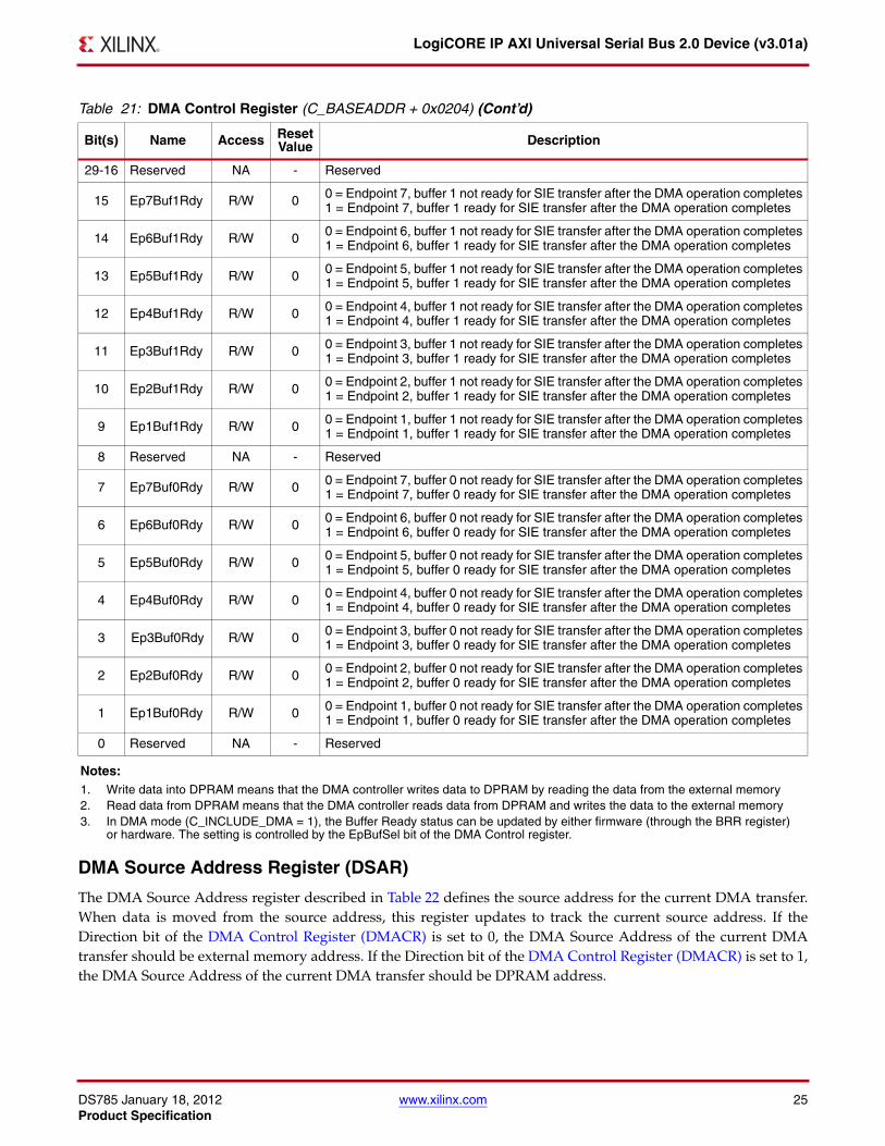
DMA Control Register (DMACR)
The DMA Control Register (DMACR) described in Table 21 defines the direction of the transfer as either Read orWrite to DPRAM2. The EpBufSel bit determines whether the SIE side Buffer Ready status is updated by Hardwarewhen the DMA is complete or by firmware through the BRR register. If EpBufSel is set to 1, the DMA Controllerupdates Buffer Ready status to the SIE based on bits [16:31] of the register at the end of a successful DMA transferonly.
Table 19: ULPI PHY Access Register (C_BASEADDR + 0x0120) (1)(2)(3)
Bit(s) Name Access Reset Value Description
31 busy R 0 0 = SIE is not busy1 = SIE is busy
30-16 Reserved NA - Reserved
15-8 PHYRdWrData R/W 0x0 PHY register read or write data
7 Reserved NA - Reserved
6 WriteNotRead R/W 0 0 = SIE reads the PHY register1 = SIE writes the PHY register
5-0 PHYRegAddr R/W 0x0 PHY register address
Notes: 1. The SIE performs the register access onto the ULPI PHY register when ULPI Bus is IDLE (for example, when there is no data
exchange between the ULPI PHY and the SIE). If the ULPI Bus is busy with ongoing data transfer, the SIE waits for ULPI Bus IDLE to perform the ULPI PHY register access.
2. Unsuccessful writes to the ULPI PHY access register result when the busy bit is set to ‘1’.3. ULPI PHY register access is not supported without assertion of MASTER_ENABLE bit of Control Register (CR).
Table 20: DMA Software Reset Register (C_BASEADDR + 0x0200)
Bit(s) Name Access Reset Value Description
31-0 DmaRst W NA A write of 0x0000000A causes the reset to the DMA modules.
Table 21: DMA Control Register (C_BASEADDR + 0x0204)
Bit(s) Name Access ResetValue Description
31 Direction(1) (2) R/W 0 0 = Write data into DPRAM21 = Read data from DPRAM2
30 EpBufSel(3) R/W 0 0 = Buffer Ready set by Firmware1 = Buffer Ready set by DMA Controller
DS785 January 18, 2012 www.xilinx.com 25Product Specification
LogiCORE IP AXI Universal Serial Bus 2.0 Device (v3.01a)
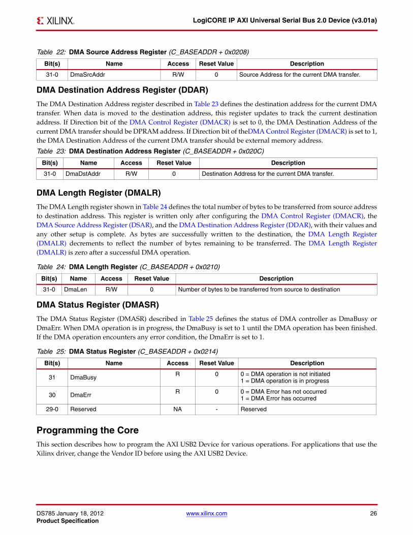
DMA Source Address Register (DSAR)
The DMA Source Address register described in Table 22 defines the source address for the current DMA transfer.When data is moved from the source address, this register updates to track the current source address. If theDirection bit of the DMA Control Register (DMACR) is set to 0, the DMA Source Address of the current DMAtransfer should be external memory address. If the Direction bit of the DMA Control Register (DMACR) is set to 1,the DMA Source Address of the current DMA transfer should be DPRAM address.
29-16 Reserved NA - Reserved
15 Ep7Buf1Rdy R/W 0 0 = Endpoint 7, buffer 1 not ready for SIE transfer after the DMA operation completes1 = Endpoint 7, buffer 1 ready for SIE transfer after the DMA operation completes
14 Ep6Buf1Rdy R/W 0 0 = Endpoint 6, buffer 1 not ready for SIE transfer after the DMA operation completes1 = Endpoint 6, buffer 1 ready for SIE transfer after the DMA operation completes
13 Ep5Buf1Rdy R/W 0 0 = Endpoint 5, buffer 1 not ready for SIE transfer after the DMA operation completes1 = Endpoint 5, buffer 1 ready for SIE transfer after the DMA operation completes
12 Ep4Buf1Rdy R/W 0 0 = Endpoint 4, buffer 1 not ready for SIE transfer after the DMA operation completes1 = Endpoint 4, buffer 1 ready for SIE transfer after the DMA operation completes
11 Ep3Buf1Rdy R/W 0 0 = Endpoint 3, buffer 1 not ready for SIE transfer after the DMA operation completes1 = Endpoint 3, buffer 1 ready for SIE transfer after the DMA operation completes
10 Ep2Buf1Rdy R/W 0 0 = Endpoint 2, buffer 1 not ready for SIE transfer after the DMA operation completes1 = Endpoint 2, buffer 1 ready for SIE transfer after the DMA operation completes
9 Ep1Buf1Rdy R/W 0 0 = Endpoint 1, buffer 1 not ready for SIE transfer after the DMA operation completes1 = Endpoint 1, buffer 1 ready for SIE transfer after the DMA operation completes
8 Reserved NA - Reserved
7 Ep7Buf0Rdy R/W 0 0 = Endpoint 7, buffer 0 not ready for SIE transfer after the DMA operation completes1 = Endpoint 7, buffer 0 ready for SIE transfer after the DMA operation completes
6 Ep6Buf0Rdy R/W 0 0 = Endpoint 6, buffer 0 not ready for SIE transfer after the DMA operation completes1 = Endpoint 6, buffer 0 ready for SIE transfer after the DMA operation completes
5 Ep5Buf0Rdy R/W 0 0 = Endpoint 5, buffer 0 not ready for SIE transfer after the DMA operation completes1 = Endpoint 5, buffer 0 ready for SIE transfer after the DMA operation completes
4 Ep4Buf0Rdy R/W 0 0 = Endpoint 4, buffer 0 not ready for SIE transfer after the DMA operation completes1 = Endpoint 4, buffer 0 ready for SIE transfer after the DMA operation completes
3 Ep3Buf0Rdy R/W 0 0 = Endpoint 3, buffer 0 not ready for SIE transfer after the DMA operation completes1 = Endpoint 3, buffer 0 ready for SIE transfer after the DMA operation completes
2 Ep2Buf0Rdy R/W 0 0 = Endpoint 2, buffer 0 not ready for SIE transfer after the DMA operation completes1 = Endpoint 2, buffer 0 ready for SIE transfer after the DMA operation completes
1 Ep1Buf0Rdy R/W 0 0 = Endpoint 1, buffer 0 not ready for SIE transfer after the DMA operation completes1 = Endpoint 1, buffer 0 ready for SIE transfer after the DMA operation completes
0 Reserved NA - Reserved
Notes: 1. Write data into DPRAM means that the DMA controller writes data to DPRAM by reading the data from the external memory2. Read data from DPRAM means that the DMA controller reads data from DPRAM and writes the data to the external memory3. In DMA mode (C_INCLUDE_DMA = 1), the Buffer Ready status can be updated by either firmware (through the BRR register)
or hardware. The setting is controlled by the EpBufSel bit of the DMA Control register.
Table 21: DMA Control Register (C_BASEADDR + 0x0204) (Cont’d)
Bit(s) Name Access ResetValue Description
DS785 January 18, 2012 www.xilinx.com 26Product Specification
LogiCORE IP AXI Universal Serial Bus 2.0 Device (v3.01a)
DMA Destination Address Register (DDAR)
The DMA Destination Address register described in Table 23 defines the destination address for the current DMAtransfer. When data is moved to the destination address, this register updates to track the current destinationaddress. If Direction bit of the DMA Control Register (DMACR) is set to 0, the DMA Destination Address of thecurrent DMA transfer should be DPRAM address. If Direction bit of theDMA Control Register (DMACR) is set to 1,the DMA Destination Address of the current DMA transfer should be external memory address.
DMA Length Register (DMALR)
The DMA Length register shown in Table 24 defines the total number of bytes to be transferred from source addressto destination address. This register is written only after configuring the DMA Control Register (DMACR), theDMA Source Address Register (DSAR), and the DMA Destination Address Register (DDAR), with their values andany other setup is complete. As bytes are successfully written to the destination, the DMA Length Register(DMALR) decrements to reflect the number of bytes remaining to be transferred. The DMA Length Register(DMALR) is zero after a successful DMA operation.
DMA Status Register (DMASR)
The DMA Status Register (DMASR) described in Table 25 defines the status of DMA controller as DmaBusy orDmaErr. When DMA operation is in progress, the DmaBusy is set to 1 until the DMA operation has been finished.If the DMA operation encounters any error condition, the DmaErr is set to 1.
Programming the CoreThis section describes how to program the AXI USB2 Device for various operations. For applications that use theXilinx driver, change the Vendor ID before using the AXI USB2 Device.
Table 22: DMA Source Address Register (C_BASEADDR + 0x0208)
Bit(s) Name Access Reset Value Description
31-0 DmaSrcAddr R/W 0 Source Address for the current DMA transfer.
Table 23: DMA Destination Address Register (C_BASEADDR + 0x020C)
Bit(s) Name Access Reset Value Description
31-0 DmaDstAddr R/W 0 Destination Address for the current DMA transfer.
Table 24: DMA Length Register (C_BASEADDR + 0x0210)
Bit(s) Name Access Reset Value Description
31-0 DmaLen R/W 0 Number of bytes to be transferred from source to destination
Table 25: DMA Status Register (C_BASEADDR + 0x0214)
Bit(s) Name Access Reset Value Description
31 DmaBusy R 0 0 = DMA operation is not initiated1 = DMA operation is in progress
30 DmaErr R 0 0 = DMA Error has not occurred1 = DMA Error has occurred
29-0 Reserved NA - Reserved
DS785 January 18, 2012 www.xilinx.com 27Product Specification
LogiCORE IP AXI Universal Serial Bus 2.0 Device (v3.01a)
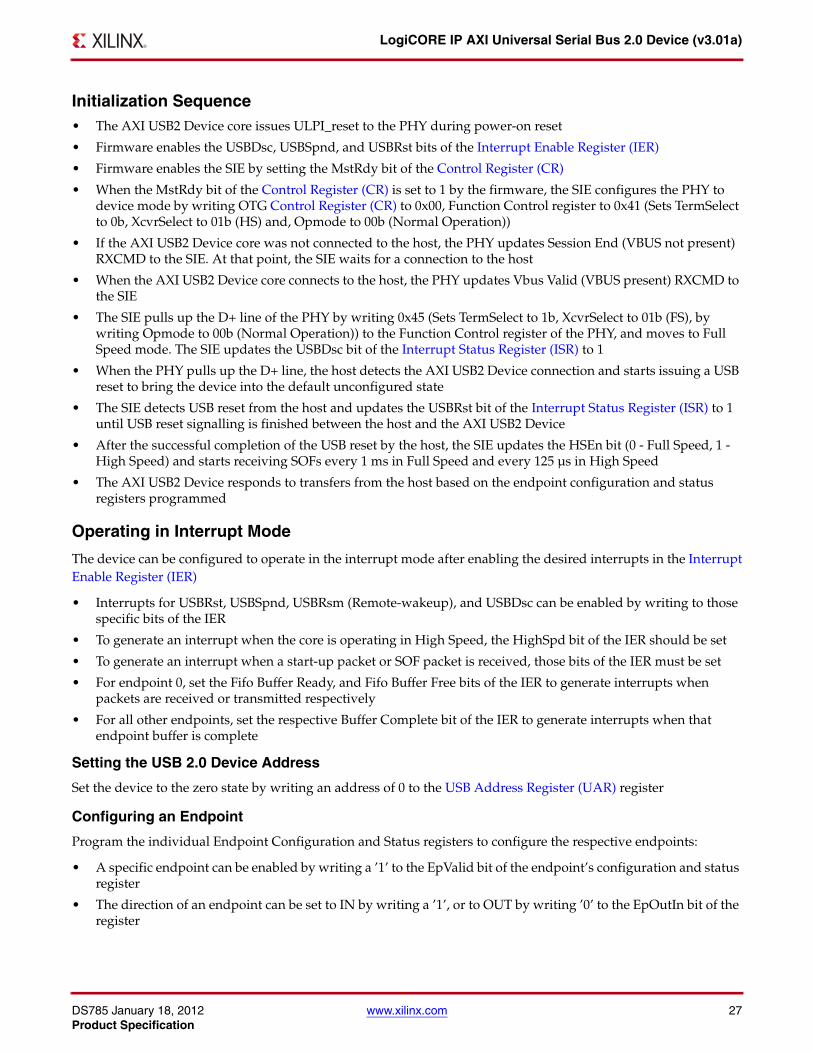
Initialization Sequence• The AXI USB2 Device core issues ULPI_reset to the PHY during power-on reset
• Firmware enables the USBDsc, USBSpnd, and USBRst bits of the Interrupt Enable Register (IER)
• Firmware enables the SIE by setting the MstRdy bit of the Control Register (CR)
• When the MstRdy bit of the Control Register (CR) is set to 1 by the firmware, the SIE configures the PHY to device mode by writing OTG Control Register (CR) to 0x00, Function Control register to 0x41 (Sets TermSelect to 0b, XcvrSelect to 01b (HS) and, Opmode to 00b (Normal Operation))
• If the AXI USB2 Device core was not connected to the host, the PHY updates Session End (VBUS not present) RXCMD to the SIE. At that point, the SIE waits for a connection to the host
• When the AXI USB2 Device core connects to the host, the PHY updates Vbus Valid (VBUS present) RXCMD to the SIE
• The SIE pulls up the D+ line of the PHY by writing 0x45 (Sets TermSelect to 1b, XcvrSelect to 01b (FS), by writing Opmode to 00b (Normal Operation)) to the Function Control register of the PHY, and moves to Full Speed mode. The SIE updates the USBDsc bit of the Interrupt Status Register (ISR) to 1
• When the PHY pulls up the D+ line, the host detects the AXI USB2 Device connection and starts issuing a USB reset to bring the device into the default unconfigured state
• The SIE detects USB reset from the host and updates the USBRst bit of the Interrupt Status Register (ISR) to 1 until USB reset signalling is finished between the host and the AXI USB2 Device
• After the successful completion of the USB reset by the host, the SIE updates the HSEn bit (0 - Full Speed, 1 - High Speed) and starts receiving SOFs every 1 ms in Full Speed and every 125 µs in High Speed
• The AXI USB2 Device responds to transfers from the host based on the endpoint configuration and status registers programmed
Operating in Interrupt Mode
The device can be configured to operate in the interrupt mode after enabling the desired interrupts in the InterruptEnable Register (IER)
• Interrupts for USBRst, USBSpnd, USBRsm (Remote-wakeup), and USBDsc can be enabled by writing to those specific bits of the IER
• To generate an interrupt when the core is operating in High Speed, the HighSpd bit of the IER should be set
• To generate an interrupt when a start-up packet or SOF packet is received, those bits of the IER must be set
• For endpoint 0, set the Fifo Buffer Ready, and Fifo Buffer Free bits of the IER to generate interrupts when packets are received or transmitted respectively
• For all other endpoints, set the respective Buffer Complete bit of the IER to generate interrupts when that endpoint buffer is complete
Setting the USB 2.0 Device Address
Set the device to the zero state by writing an address of 0 to the USB Address Register (UAR) register
Configuring an Endpoint
Program the individual Endpoint Configuration and Status registers to configure the respective endpoints:
• A specific endpoint can be enabled by writing a ’1’ to the EpValid bit of the endpoint’s configuration and status register
• The direction of an endpoint can be set to IN by writing a ’1’, or to OUT by writing ’0’ to the EpOutIn bit of the register
DS785 January 18, 2012 www.xilinx.com 28Product Specification
LogiCORE IP AXI Universal Serial Bus 2.0 Device (v3.01a)
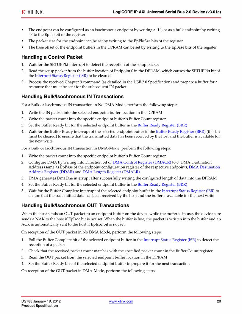
• The endpoint can be configured as an isochronous endpoint by writing a ’1’ , or as a bulk endpoint by writing ’0’ to the EpIso bit of the register
• The packet size for the endpoint can be set by writing to the EpPktSze bits of the register
• The base offset of the endpoint buffers in the DPRAM can be set by writing to the EpBase bits of the register
Handling a Control Packet1. Wait for the SETUPPkt interrupt to detect the reception of the setup packet
2. Read the setup packet from the buffer location of Endpoint 0 in the DPRAM, which causes the SETUPPkt bit of the Interrupt Status Register (ISR) to be cleared
3. Process the received Chapter 9 command (as detailed in the USB 2.0 Specification) and prepare a buffer for a response that must be sent for the subsequent IN packet
Handling Bulk/Isochronous IN Transactions
For a Bulk or Isochronous IN transaction in No DMA Mode, perform the following steps:
1. Write the IN packet into the selected endpoint buffer location in the DPRAM
2. Write the packet count into the specific endpoint buffer’s Buffer Count register
3. Set the Buffer Ready bit for the selected endpoint buffer in the Buffer Ready Register (BRR)
4. Wait for the Buffer Ready interrupt of the selected endpoint buffer in the Buffer Ready Register (BRR) (this bit must be cleared) to ensure that the transmitted data has been received by the host and the buffer is available for the next write
For a Bulk or Isochronous IN transaction in DMA-Mode, perform the following steps:
1. Write the packet count into the specific endpoint buffer’s Buffer Count register
2. Configure DMA by writing into Direction bit of DMA Control Register (DMACR) to 0, DMA Destination Address (same as EpBase of the endpoint configuration register of the respective endpoint), DMA Destination Address Register (DDAR) and DMA Length Register (DMALR)
3. DMA generates DmaDne interrupt after successfully writing the configured length of data into the DPRAM
4. Set the Buffer Ready bit for the selected endpoint buffer in the Buffer Ready Register (BRR)
5. Wait for the Buffer Complete interrupt of the selected endpoint buffer in the Interrupt Status Register (ISR) to ensure that the transmitted data has been received by the host and the buffer is available for the next write
Handling Bulk/Isochronous OUT Transactions
When the host sends an OUT packet to an endpoint buffer on the device while the buffer is in use, the device coresends a NAK to the host if EpIsoc bit is not set. When the buffer is free, the packet is written into the buffer and anACK is automatically sent to the host if EpIsoc bit is not set.
On reception of the OUT packet in No DMA Mode, perform the following steps:
1. Poll the Buffer Complete bit of the selected endpoint buffer in the Interrupt Status Register (ISR) to detect the reception of a packet
2. Check that the received packet count matches with the specified packet count in the Buffer Count register
3. Read the OUT packet from the selected endpoint buffer location in the DPRAM
4. Set the Buffer Ready bits of the selected endpoint buffer to prepare it for the next transaction
On reception of the OUT packet in DMA-Mode, perform the following steps:
DS785 January 18, 2012 www.xilinx.com 29Product Specification
LogiCORE IP AXI Universal Serial Bus 2.0 Device (v3.01a)
1. Poll the Buffer Complete bit of the selected endpoint buffer in the Interrupt Status Register (ISR) to detect the reception of a packet
2. Check the received packet count matches with the specified packet count in the Buffer Count register
3. Read the OUT packet by configure DMA by writing into Direction bit of DMA Control Register (DMACR) to 1, DMA Source Address Register (DSAR) (same as EpBase of the endpoint configuration register of the respective endpoint), DMA Destination Address Register (DDAR) and DMA Length Register (DMALR)
4. DMA generates DmaDne interrupt after successfully reading the configured length of data into the DPRAM2
5. Set the Buffer Ready bits of the selected endpoint buffer to prepare it for the next transaction
USB Reset Signalling
When the host wants to start communicating with a device it starts by applying a 'reset' condition which sets thedevice to its default unconfigured state. This 'reset' should not be confused with a micro-controller power-on typereset. It is a USB protocol reset to ensure that the device USB signalling starts from a known state. The High Speedcapable AXI USB2 Device core can be reset while the device in the Powered, Default, Address, Configured orSuspended states. The AXI USB2 Device can be successfully reset by any host (even an USB1.x host).
The host performs USB reset Signalling High Speed capable AXI USB2 Device as follows
1. The host drives SE0; the start of SE0 is referred to as time T0.
2. The SIE detects assertion of SE0.
a. If the SIE detects SE0 from the USB Suspend state, then the SIE begins the High Speed handshake detection after the detection of SE0 for no less than 2.5 us
b. If the SIE detects SE0 from a non-suspended Full Speed mode, the SIE begins a High Speed handshake detection after the detection of SE0 for no less than 2.5 us and no more than 3.0 ms
c. If the SIE detects SE0 from a non-suspended High Speed mode, the SIE wait for 3.0 ms before reverting to Full Speed mode. After reverting to Full Speed, the SIE checks the line state update from the PHY for SE0 (to check whether the host has issued suspend or USB reset), no less than 1 ms from the point the SIE reverted to Full Speed. If the SIE detects SE0 by the RXCMD updating from the PHY, the SIE begins the High Speed handshake detection.
3. Because the AXI USB2 Device is a High Speed capable device, the SIE follows High Speed Handshake Detection protocol.

DS785 January 18, 2012 www.xilinx.com 30Product Specification
LogiCORE IP AXI Universal Serial Bus 2.0 Device (v3.01a)
X-Ref Target - Figure 2
Figure 2: USB Reset Signalling with USB1.x Host - Full Speed
X-Ref Target - Figure 3
Figure 3: USB Reset Signalling with USB2.0 Host - High Speed Handshaking
VBUS detect
ulpi_data[7:0]
ulpi_dir
ulpi_nxt
ulpi_stp
XcvrSelect
TermSelect
OpMode
LineStae
USB Reset
HSEn
SEO
00
K K K…
Host drives
01(FS)
J(01b) SEO(00b)SEO(00b)
01(FS)00(HS)
01(Chirp)
SIE(Chirp K(10b)
00(normal)
Device Responds Host Responds FSIDLE
FS - J
J
DS785_02
TXCMDRegWr
TXCMDRegWr
TXCMDNOPID
00(normal)
DS785_03
VBUS detect
ulpi_data[7:0]
ulpi_dir
ulpi_nxt
ulpi_stp
XcvrSelect
TermSelect
OpMode
LineStae
USB Reset
HSEn
SEO
00
K K K K K K…
Host drives
01(FS)
J(01b)
Squelch(00b)
SEO(00b)
01(FS)00(HS)
10(Chirp)
SIE(Chirp K(10b) Host (Chirp K/J (10b/01b)
Device Responds Host Responds HSIDLE
JJ J
00
Squelch(00b)
!Squelch(01b)
TXCMDRegWr
TXCMDRegWr
TXCMDNOPID
00(normal) 00(normal)
DS785 January 18, 2012 www.xilinx.com 31Product Specification
LogiCORE IP AXI Universal Serial Bus 2.0 Device (v3.01a)
High Speed Handshake Detection Protocol1. The SIE writes 0x54 (sets XcvrSelect to 00b, TermSelect to 1b and Opmode to 10b (Chirping)) to the Function
Control register of the PHY
2. Immediately after the write, the SIE puts TXCMD as 0x40 (NOPID) and starts transmitting a chirpK for 2 ms
3. After 2 ms of ChirpK transmission, the PHY updates RXCMD with line state as SE0
4. The SIE detects SE0 and waits for 100 us to look for a High Speed host chirp, for example, an alternating sequence of ChirpKs and ChirpJs
5. If the SIE does not observe any High Speed host chirp, the SIE configures the PHY to Full Speed mode by writing 0x45 (sets XcvrSelect to 01b, TermSelect to, 1b, and Opmode to 00b (Normal Operation)) to the Function Control register of the PHY. At this point, the SIE is in Full Speed mode and waits for Full Speed USB traffic from the host.
6. If the SIE observes the High Speed host chirp, the SIE checks for a minimum of chirp K-J-K-J-K-J
7. The SIE also checks each individual chirpK and chirpJ for at least 2.5 us
8. After detecting the minimum sequence, the SIE configures the PHY to High Speed mode by writing 0x40 (Sets TermSelect to 0b, XcvrSelect to 00b (HS) and Opmode to 00b (Normal Operation)) to the Function Control register of the PHY and updates the HSEn bit of the Interrupt Status Register (ISR) to 1.
9. At this point, the SIE is in High Speed mode and sees line-state as !squelch (linestate != 00) on the RXCMD update.
10. If the SIE observes squelch as linestate update from the PHY (for example, RXCMD[1:0]), the SIE treats that the host has completed the chirp and stops updating the status as USBRst in the Interrupt Status Register (ISR).
11. Now the SIE waits for High Speed USB traffic from the host.
Suspend Signalling
When the host does not want to continue any further communication with the connected device, it keeps the AXIUSB2 Device in the suspend mode by ceasing all of its transmissions (including SOFs). The AXI USB2 Devicerecognizes the suspend condition in High Speed mode as follows:
1. Initially, the host and the AXI USB2 Device are either in Full Speed or High Speed mode.
2. When the SIE sees no bus activity for 3 ms, it enters Full Speed mode by writing 0x45 (Sets TermSelect to 1b, XcvrSelect to 01b (FS), and Opmode to 00b (Normal Operation)) to the Function Control register.
3. After 1 ms, the SIE samples the line state from the RXCMD update of the PHY.
4. If the line state is Full Speed J, the SIE enters into the Suspend state after 7 ms and updates the status as suspended by asserting the USBSpnd bit of the Interrupt Status Register (ISR).
5. The SIE is now SIE in the Suspended state.
6. Resume or USB reset signalling can bring the SIE out from suspended state.
Resume Signalling
When the AXI USB2 Device in the suspend state, host wakeup the device with a resume signalling. The AXI USB2Device detects Resume signalling as listed in the steps:
1. When both the host and the AXI USB2 Device are in Low Power mode
2. If the SIE observes Full Speed K as line state (that is, RXCMD[1:0]) update from the PHY then the SIE treats it as Resume signalling from the PHY and updates the status as Resume by setting USBRsm bit of the Interrupt Status Register (ISR).
3. The SIE waits to detect the End of Resume, that is, SE0 as line state update from the PHY
4. If the SIE detects SE0 linestate update from the PHY:
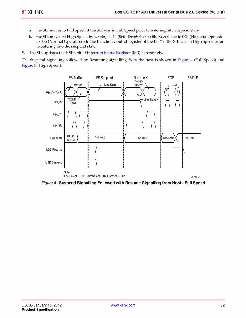
DS785 January 18, 2012 www.xilinx.com 32Product Specification
LogiCORE IP AXI Universal Serial Bus 2.0 Device (v3.01a)
a. the SIE moves to Full Speed if the SIE was in Full Speed prior to entering into suspend state
b. the SIE moves to High Speed by writing 0x40 (Sets TermSelect to 0b, XcvrSelect to 00b (HS), and Opmode to 00b (Normal Operation)) to the Function Control register of the PHY if the SIE was in High Speed prior to entering into the suspend state
5. The SIE updates the HSEn bit of Interrupt Status Register (ISR) accordingly.
The Suspend signalling followed by Resuming signalling from the host is shown in Figure 4 (Full Speed) andFigure 5 (High Speed).
X-Ref Target - Figure 4
Figure 4: Suspend Signalling Followed with Resume Signalling from Host - Full Speed
DS785_04
FS Traffic
ulpi_data[7:0]
ulpi_dir
ulpi_nxt
ulpi_stp
Note:XcvrSelect = 01b, TermSelect = 1b, OpMode = 00b.
Line State
Line State
USB Resume
USB Suspend
SEO
FS Suspend
FSJ (01b)FSJ/K(01/10) FSJ (01b)FSK (10b) SEO(00b)
Resume K EOP FSIDLE
J
TXCMDRegWr
TXCMDRegWrTXCMD
Line State K
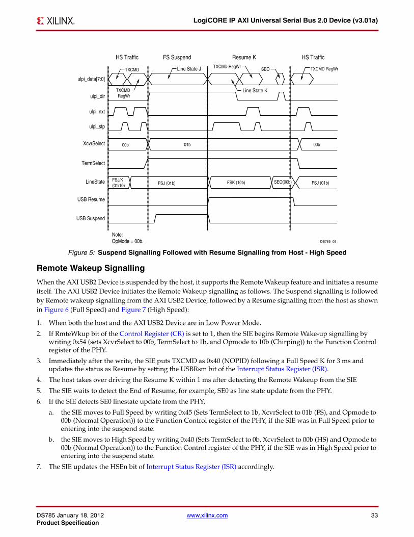
DS785 January 18, 2012 www.xilinx.com 33Product Specification
LogiCORE IP AXI Universal Serial Bus 2.0 Device (v3.01a)
Remote Wakeup Signalling
When the AXI USB2 Device is suspended by the host, it supports the Remote Wakeup feature and initiates a resumeitself. The AXI USB2 Device initiates the Remote Wakeup signalling as follows. The Suspend signalling is followedby Remote wakeup signalling from the AXI USB2 Device, followed by a Resume signalling from the host as shownin Figure 6 (Full Speed) and Figure 7 (High Speed):
1. When both the host and the AXI USB2 Device are in Low Power Mode.
2. If RmteWkup bit of the Control Register (CR) is set to 1, then the SIE begins Remote Wake-up signalling by writing 0x54 (sets XcvrSelect to 00b, TermSelect to 1b, and Opmode to 10b (Chirping)) to the Function Control register of the PHY.
3. Immediately after the write, the SIE puts TXCMD as 0x40 (NOPID) following a Full Speed K for 3 ms and updates the status as Resume by setting the USBRsm bit of the Interrupt Status Register (ISR).
4. The host takes over driving the Resume K within 1 ms after detecting the Remote Wakeup from the SIE
5. The SIE waits to detect the End of Resume, for example, SE0 as line state update from the PHY.
6. If the SIE detects SE0 linestate update from the PHY,
a. the SIE moves to Full Speed by writing 0x45 (Sets TermSelect to 1b, XcvrSelect to 01b (FS), and Opmode to 00b (Normal Operation)) to the Function Control register of the PHY, if the SIE was in Full Speed prior to entering into the suspend state.
b. the SIE moves to High Speed by writing 0x40 (Sets TermSelect to 0b, XcvrSelect to 00b (HS) and Opmode to 00b (Normal Operation)) to the Function Control register of the PHY, if the SIE was in High Speed prior to entering into the suspend state.
7. The SIE updates the HSEn bit of Interrupt Status Register (ISR) accordingly.
X-Ref Target - Figure 5
Figure 5: Suspend Signalling Followed with Resume Signalling from Host - High Speed
DS785_05
HS Traffic
Note:OpMode = 00b.
Line State J SEO
FS Suspend
FSJ (01b)FSJ/K(01/10) FSJ (01b)FSK (10b)
Resume K HS Traffic
TXCMDRegWr
TXCMD RegWr TXCMD RegWrTXCMD
Line State K
ulpi_data[7:0]
ulpi_dir
ulpi_nxt
ulpi_stp
XcvrSelect
TermSelect
LineState
USB Resume
USB Suspend
SEO(00b)
00b 00b01b
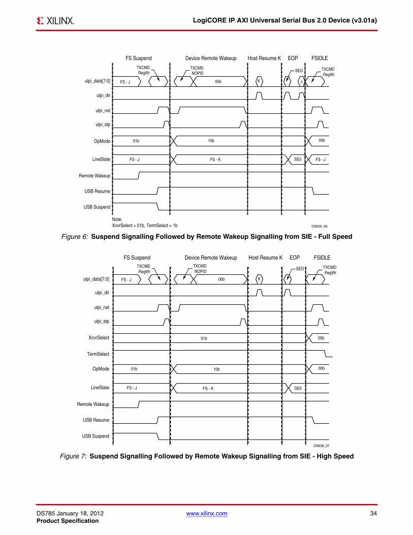
DS785 January 18, 2012 www.xilinx.com 34Product Specification
LogiCORE IP AXI Universal Serial Bus 2.0 Device (v3.01a)
X-Ref Target - Figure 6
Figure 6: Suspend Signalling Followed by Remote Wakeup Signalling from SIE - Full Speed
X-Ref Target - Figure 7
Figure 7: Suspend Signalling Followed by Remote Wakeup Signalling from SIE - High Speed
DS639_06
FS Suspend
ulpi_data[7:0]
ulpi_dir
ulpi_nxt
ulpi_stp
OpMode
LineState
Remote Wakeup
USB Resume
USB Suspend
SEO
00b K
Device Remote Wakeup
FS - J
01b 10b 00b
FS - K FS - J
FS - J
SE0
Host Resume K EOP FSIDLE
J
TXCMDRegWr
TXCMDRegWr
TXCMDNOPID
Note:XcvrSelect = 01b, TermSelect = 1b
DS639_07
ulpi_data[7:0]
ulpi_dir
ulpi_nxt
ulpi_stp
XcvrSelect
TermSelect
OpMode
LineState
Remote Wakeup
USB Resume
USB Suspend
FS Suspend
SEO
00b K
Device Remote Wakeup
FS - J
01b
01b
10b 00b
00b
FS - K
FS - J
SE0
Host Resume K EOP FSIDLETXCMDRegWr
TXCMDRegWr
TXCMDNOPID
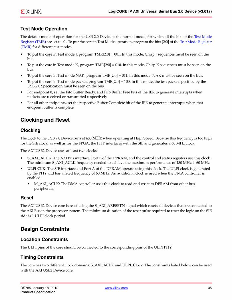
DS785 January 18, 2012 www.xilinx.com 35Product Specification
LogiCORE IP AXI Universal Serial Bus 2.0 Device (v3.01a)
Test Mode Operation
The default mode of operation for the USB 2.0 Device is the normal mode, for which all the bits of the Test ModeRegister (TMR) are set to ’0’. To put the core in Test Mode operation, program the bits [2:0] of the Test Mode Register(TMR) for different test modes:
• To put the core in Test mode J, program TMR[2:0] = 001. In this mode, Chirp J sequences must be seen on the bus.
• To put the core in Test mode K, program TMR[2:0] = 010. In this mode, Chirp K sequences must be seen on the bus.
• To put the core in Test mode NAK, program TMR[2:0] = 011. In this mode, NAK must be seen on the bus.
• To put the core in Test mode packet, program TMR[2:0] = 100. In this mode, the test packet specified by the USB 2.0 Specification must be seen on the bus.
• For endpoint 0, set the Fifo Buffer Ready, and Fifo Buffer Free bits of the IER to generate interrupts when packets are received or transmitted respectively
• For all other endpoints, set the respective Buffer Complete bit of the IER to generate interrupts when that endpoint buffer is complete
Clocking and Reset
Clocking
The clock to the USB 2.0 Device runs at 480 MHz when operating at High Speed. Because this frequency is too highfor the SIE clock, as well as for the FPGA, the PHY interfaces with the SIE and generates a 60 MHz clock.
The AXI USB2 Device uses at least two clocks:
• S_AXI_ACLK: The AXI Bus interface, Port B of the DPRAM, and the control and status registers use this clock. The minimum S_AXI_ACLK frequency needed to achieve the maximum performance of 480 MHz is 60 MHz.
• ULPI CLK: The SIE interface and Port A of the DPRAM operate using this clock. The ULPI clock is generated by the PHY and has a fixed frequency of 60 MHz. An additional clock is used when the DMA controller is enabled:
• M_AXI_ACLK: The DMA controller uses this clock to read and write to DPRAM from other bus peripherals.
Reset
The AXI USB2 Device core is reset using the S_AXI_ARESETN signal which resets all devices that are connected tothe AXI Bus in the processor system. The minimum duration of the reset pulse required to reset the logic on the SIEside is 1 ULPI clock period.
Design Constraints
Location Constraints
The ULPI pins of the core should be connected to the corresponding pins of the ULPI PHY.
Timing Constraints
The core has two different clock domains: S_AXI_ACLK and ULPI_Clock. The constraints listed below can be usedwith the AXI USB2 Device core.
DS785 January 18, 2012 www.xilinx.com 36Product Specification
LogiCORE IP AXI Universal Serial Bus 2.0 Device (v3.01a)
Period Constraints for Clock Nets
The constraints below are automatically added to the system with the core’s tcl script. If the S_AXI_CLK andM_AXI_CLK clocks have a different frequency when C_INCLUDE_DMA is enabled, then similar cross clock domainconstraints between ULPI <-> SAXI, ULPI <-> MAXI, and SAXI <-> MAXI domains are added automatically by thetcl script. These constraints can be overwritten by explicitly declaring the constraints in the UCF.
ULPI_CLK
The ULPI clock input is generated through the ULPI PHY and has a fixed frequency of 60 MHz.
# Set the ULPI_CLK constraints NET “ULPI_CLK” TNM_NET = “ULPI_CLK”;TIMESPEC “TS_ULPI_CLK” = PERIOD “ULPI_CLK” 16667 ns HIGH 50%;
S_AXI_ACLK
The clock provided to S_AXI_ACLK must be constrained for a clock frequency of 60 MHz - 200 MHz.
# Set the S_AXI_ACLK constraints; This can be relaxed based on the actual frequencyNET “S_AXI_ACLK” TNM_NET = “S_AXI_ACLK”;TIMESPEC “TS_S_AXI_ACLK” = PERIOD “S_AXI_ACLK” 10 ns HIGH 50%;
ULPI Interface Constraints#offset in constraints are calculated as follows.#clock frequency is 16.667ns#ULPI PHY output delay for output clock mode for SMSC2 PHY is 3.5ns#onboard trace delay would be 1ns #input offset = (clock period - PHY outputdelay - trance delay)#with 1ns hold requirement for the PHY, considering 200ps clock jitter#OFFSET IN valid period would be 800ps.# Set the OFFSET IN delay as 12.167 ns with respect to ULPI_CLKOFFSET = IN 12.167 ns VALID 12.967 ns BEFORE ULPI_CLK RISING;# ULPI PHY setup time for output clock mode is 6ns# leaving 1ns for onboard trace delay.# OFFSET OUT = clock period - (PHY setup time + trace delay)# Set the OFFSET OUT delay as 9.667 ns with respect to ULPI_CLKOFFSET = OUT 9.667 ns AFTER ULPI_CLK RISING;# Set MAX DELAY constraint on ULPI_Dir pinNET “ULPI_Dir” MAXDELAY=4.5 ns;# Cross clock domain timing Constraints between ULPI_Clk and S_AXI_ApClk#DMA is included and both slave and master axi clock frequencies are EQUALNET “ULPI_Clock” TNM_NET = “ulpi_0_clock_net”;NET “S_AXI_AClk” TNM_NET = “saxi_0_clock_net”;TIMEGRP “ulpi_0_clock_grp” = “ulpi_0_clock_net”;TIMEGRP “saxi_0_clock_grp” = “saxi_0_clock_net”;TIMESPEC TS_saxi_0_to_ulpi_0_clk = FROM “saxi_0_clock_grp” TO “ulpi_0_clock_grp” 32.2 nsDATAPATHONLY; # (2 * ULPI Clock period - 1)TIMESPEC TS_ulpi_0_to_saxi_0_clk = FROM “ulpi_0_clock_grp” TO “saxi_0_clock_grp” 19.0 ns DATAPATHONLY; #(2 * SAXI Clock period - 1)
Additional ULPI interface constraints
Additional ULPI constraints are used in the system level UCF (system.ucf) to group the ULPI input/output signalsand for applying offset IN/OUT constraints respectively to improve the timing results. These offset constraintsoverwrite the IP level constraints.
DS785 January 18, 2012 www.xilinx.com 37Product Specification
LogiCORE IP AXI Universal Serial Bus 2.0 Device (v3.01a)
Design Implementation
Target Technology
The target technology is an FPGA listed in the Supported Device Families field of the LogiCORE IP Facts Table. TheFPGA used must have the following attributes:
• Large enough to accommodate the core.
• Contain a sufficient number of IOBs/BRAM.
Device Utilization and Performance Benchmarks
Because the AXI USB2 Device core will be used with other design modules in the FPGA, the utilization and timingnumbers reported in this section are estimates only. When this core is combined with other designs in the system,the utilization of FPGA resources and timing of the AXI USB2 Device core will vary from the results reported here.
The AXI USB2 Device core resource utilization for various parameter combinations measured with the Kintex™-7FPGA as the target device are detailed in Table 26.
#NET "axi_usb2_device_0_ULPI_Clock_pin" TNM_NET = axi_usb2_device_0_ULPI_Clock_pin;#NET "axi_usb2_device_0_ULPI_Data_pin<0>(1)" TNM = ULPI_INPUTS;#NET "axi_usb2_device_0_ULPI_Data_pin<1>(1)" TNM = ULPI_INPUTS;#NET "axi_usb2_device_0_ULPI_Data_pin<2>(1)" TNM = ULPI_INPUTS;#NET "axi_usb2_device_0_ULPI_Data_pin<3>(1)" TNM = ULPI_INPUTS;#NET "axi_usb2_device_0_ULPI_Data_pin<4>(1)" TNM = ULPI_INPUTS;#NET "axi_usb2_device_0_ULPI_Data_pin<5>(1)" TNM = ULPI_INPUTS;#NET "axi_usb2_device_0_ULPI_Data_pin<6>(1)" TNM = ULPI_INPUTS;#NET "axi_usb2_device_0_ULPI_Data_pin<7>(1)" TNM = ULPI_INPUTS;#NET "axi_usb2_device_0_ULPI_Dir_pin(1)" TNM = ULPI_INPUTS;#NET "axi_usb2_device_0_ULPI_Next_pin(1)" TNM = ULPI_INPUTS;#TIMEGRP "ULPI_INPUTS" OFFSET = IN 12.167 ns VALID 12.967 ns BEFORE "axi_usb2_device_0_ULPI_Clock_pin" RISING;#NET "axi_usb2_device_0_ULPI_Data_pin<7>(1)" TNM = ULPI_OUTPUTS;#NET "axi_usb2_device_0_ULPI_Data_pin<6>(1)" TNM = ULPI_OUTPUTS;#NET "axi_usb2_device_0_ULPI_Data_pin<5>(1)" TNM = ULPI_OUTPUTS;#NET "axi_usb2_device_0_ULPI_Data_pin<4>(1)" TNM = ULPI_OUTPUTS;#NET "axi_usb2_device_0_ULPI_Data_pin<3>(1)" TNM = ULPI_OUTPUTS;#NET "axi_usb2_device_0_ULPI_Data_pin<2>(1)" TNM = ULPI_OUTPUTS;#NET "axi_usb2_device_0_ULPI_Data_pin<1>(1)" TNM = ULPI_OUTPUTS;#NET "axi_usb2_device_0_ULPI_Data_pin<0>(1)" TNM = ULPI_OUTPUTS;#NET "axi_usb2_device_0_ULPI_Stop_pin(1)" TNM = ULPI_OUTPUTS;#TIMEGRP "ULPI_OUTPUTS" OFFSET = OUT 9.667 ns AFTER "axi_usb2_device_0_ULPI_Clock_pin" RISING;
1.Replace the net name with the name used in the system.
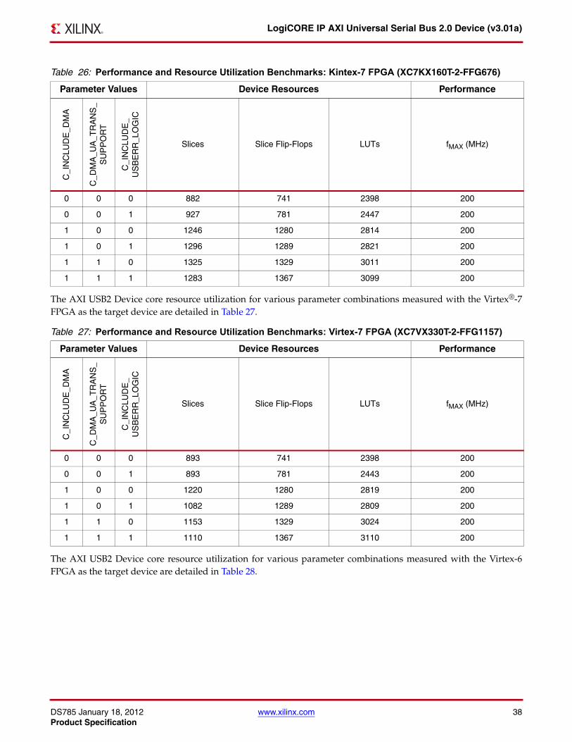
DS785 January 18, 2012 www.xilinx.com 38Product Specification
LogiCORE IP AXI Universal Serial Bus 2.0 Device (v3.01a)
The AXI USB2 Device core resource utilization for various parameter combinations measured with the Virtex®-7FPGA as the target device are detailed in Table 27.
The AXI USB2 Device core resource utilization for various parameter combinations measured with the Virtex-6FPGA as the target device are detailed in Table 28.
Table 26: Performance and Resource Utilization Benchmarks: Kintex-7 FPGA (XC7KX160T-2-FFG676)
Parameter Values Device Resources Performance
C_I
NC
LUD
E_D
MA
C_D
MA
_UA
_TR
AN
S_
SU
PP
OR
T
C_I
NC
LUD
E_
US
BE
RR
_LO
GIC
Slices Slice Flip-Flops LUTs fMAX (MHz)
0 0 0 882 741 2398 200
0 0 1 927 781 2447 200
1 0 0 1246 1280 2814 200
1 0 1 1296 1289 2821 200
1 1 0 1325 1329 3011 200
1 1 1 1283 1367 3099 200
Table 27: Performance and Resource Utilization Benchmarks: Virtex-7 FPGA (XC7VX330T-2-FFG1157)
Parameter Values Device Resources Performance
C_I
NC
LUD
E_D
MA
C_D
MA
_UA
_TR
AN
S_
SU
PP
OR
T
C_I
NC
LUD
E_
US
BE
RR
_LO
GIC
Slices Slice Flip-Flops LUTs fMAX (MHz)
0 0 0 893 741 2398 200
0 0 1 893 781 2443 200
1 0 0 1220 1280 2819 200
1 0 1 1082 1289 2809 200
1 1 0 1153 1329 3024 200
1 1 1 1110 1367 3110 200
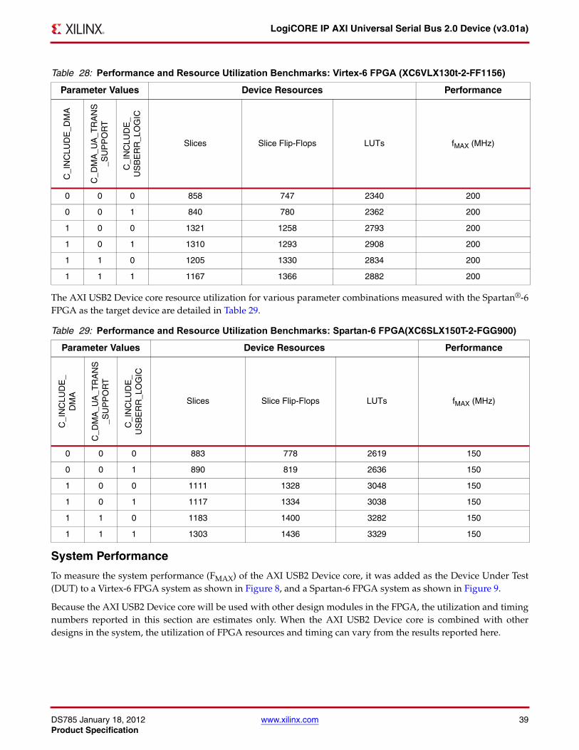
DS785 January 18, 2012 www.xilinx.com 39Product Specification
LogiCORE IP AXI Universal Serial Bus 2.0 Device (v3.01a)
The AXI USB2 Device core resource utilization for various parameter combinations measured with the Spartan®-6FPGA as the target device are detailed in Table 29.
System Performance
To measure the system performance (FMAX) of the AXI USB2 Device core, it was added as the Device Under Test(DUT) to a Virtex-6 FPGA system as shown in Figure 8, and a Spartan-6 FPGA system as shown in Figure 9.
Because the AXI USB2 Device core will be used with other design modules in the FPGA, the utilization and timingnumbers reported in this section are estimates only. When the AXI USB2 Device core is combined with otherdesigns in the system, the utilization of FPGA resources and timing can vary from the results reported here.
Table 28: Performance and Resource Utilization Benchmarks: Virtex-6 FPGA (XC6VLX130t-2-FF1156)
Parameter Values Device Resources Performance
C_I
NC
LUD
E_D
MA
C_D
MA
_UA
_TR
AN
S_S
UP
PO
RT
C_I
NC
LUD
E_
US
BE
RR
_LO
GIC
Slices Slice Flip-Flops LUTs fMAX (MHz)
0 0 0 858 747 2340 200
0 0 1 840 780 2362 200
1 0 0 1321 1258 2793 200
1 0 1 1310 1293 2908 200
1 1 0 1205 1330 2834 200
1 1 1 1167 1366 2882 200
Table 29: Performance and Resource Utilization Benchmarks: Spartan-6 FPGA(XC6SLX150T-2-FGG900)
Parameter Values Device Resources Performance
C_I
NC
LUD
E_
DM
A
C_D
MA
_UA
_TR
AN
S_S
UP
PO
RT
C_I
NC
LUD
E_
US
BE
RR
_LO
GIC
Slices Slice Flip-Flops LUTs fMAX (MHz)
0 0 0 883 778 2619 150
0 0 1 890 819 2636 150
1 0 0 1111 1328 3048 150
1 0 1 1117 1334 3038 150
1 1 0 1183 1400 3282 150
1 1 1 1303 1436 3329 150
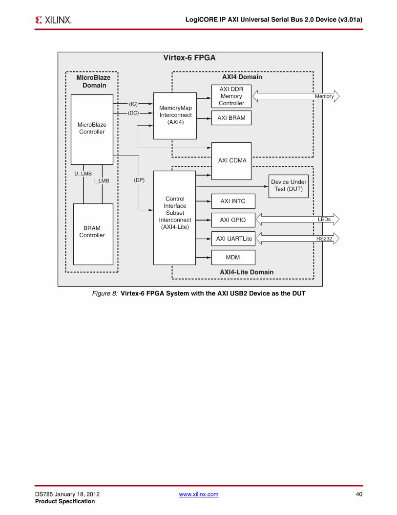
DS785 January 18, 2012 www.xilinx.com 40Product Specification
LogiCORE IP AXI Universal Serial Bus 2.0 Device (v3.01a)
X-Ref Target - Figure 8
Figure 8: Virtex-6 FPGA System with the AXI USB2 Device as the DUT
AXI4-Lite Domain
MicroBlazeController
AXI INTC
AXI GPIO
AXI UARTLite
AXI DDRMemory
Controller
MDM
MicroBlaze Domain
AXI4 Domain
BRAMController
D_LMBI_LMB
(IC)
AXI BRAM(DC)
Device UnderTest (DUT)
Memory
(DP)
LEDs
RS232
AXI CDMA
Virtex-6 FPGA
MemoryMapInterconnect
(AXI4)
ControlInterfaceSubset
Interconnect(AXI4-Lite)
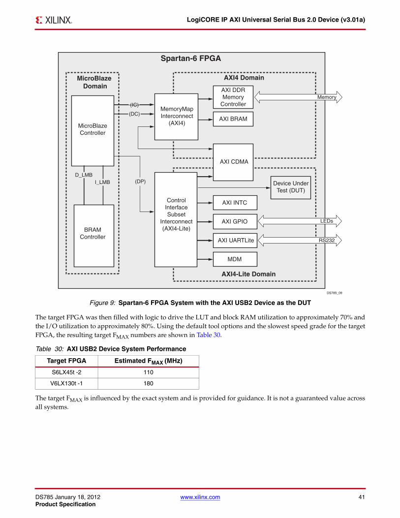
DS785 January 18, 2012 www.xilinx.com 41Product Specification
LogiCORE IP AXI Universal Serial Bus 2.0 Device (v3.01a)
The target FPGA was then filled with logic to drive the LUT and block RAM utilization to approximately 70% andthe I/O utilization to approximately 80%. Using the default tool options and the slowest speed grade for the targetFPGA, the resulting target FMAX numbers are shown in Table 30.
The target FMAX is influenced by the exact system and is provided for guidance. It is not a guaranteed value acrossall systems.
X-Ref Target - Figure 9
Figure 9: Spartan-6 FPGA System with the AXI USB2 Device as the DUT
Table 30: AXI USB2 Device System Performance
Target FPGA Estimated FMAX (MHz)
S6LX45t -2 110
V6LX130t -1 180
AXI4-Lite Domain
MicroBlazeController
AXI INTC
AXI GPIO
AXI UARTLite
AXI DDRMemory
Controller
MDM
MicroBlaze Domain
AXI4 Domain
BRAMController
D_LMBI_LMB
(IC)
AXI BRAM(DC)
Device UnderTest (DUT)
Memory
(DP)
DS785_09
LEDs
RS232
AXI CDMA
Spartan-6 FPGA
MemoryMapInterconnect
(AXI4)
ControlInterfaceSubset
Interconnect(AXI4-Lite)
DS785 January 18, 2012 www.xilinx.com 42Product Specification
LogiCORE IP AXI Universal Serial Bus 2.0 Device (v3.01a)
Throughput
To measure the system throughput of the AXI USB2 Device core, a Virtex-6 system was used similar to Figure 8 andtested on a Xilinx ML605 board.
For this test, the firmware running on the ML605 evaluation board behaved as a mass storage device. A Windowsapplication running on a Windows Desktop PC set up the mass storage device for the throughput test on its BULKIN endpoint. The Windows application has an option of selecting the amount of traffic being sent on the bus for thethroughput test. The selection options are 1MB/10MB/1000MB. When the option was selected, the Windowsapplication set up the mass storage device to send the selected amount of data. Upon completion of the datatransfer, the result was displayed on the Windows screen in MB/s. The throughput was measured using theamount of data sent over the bus and the time taken for transmission. A LeCroy USB analyzer was used to capturethe transactions on the bus. The throughput results were based on the number of USB data packets receivedbetween two SOF packets. The throughput numbers are shown in Table 31 and Table 32.
Note: In BULK IN mode, the performance of the device depends on the number of data transfer packets that the host application can initiate between the two SOFs.
Support Xilinx provides technical support for this LogiCORE™ product when used as described in the productdocumentation. Xilinx cannot guarantee timing, functionality, or support of product if implemented in devices thatare not defined in the documentation, if customized beyond that allowed in the product documentation, or ifchanges are made to any section of the design labeled DO NOT MODIFY.
Ordering InformationThis Xilinx LogiCORE IP module is provided under the terms of the Xilinx Core Site License. The core is generatedusing the Xilinx ISE® Embedded Edition software (EDK). For full access to all core functionality in simulation andin hardware, you must purchase a license for the core. Please contact your local Xilinx sales representative forinformation on pricing and availability of Xilinx LogiCORE IP.
For more information, visit the AXI USB2 Device product web page.
Information about this and other Xilinx LogiCORE IP modules is available at the Xilinx Intellectual Property page.For information on pricing and availability of other Xilinx LogiCORE modules and software, contact your localXilinx sales representative.
This Embedded IP module is provided under the terms of the Xilinx Core Site License. A free evaluation version ofthe core is included with the ISE Design Suite Embedded Edition software. Use the Xilinx Platform Studioapplication (XPS) included with the Embedded Edition software to instantiate and use this core.
For full access to all core functionality in simulation and in hardware, you must purchase a license for the core.Contact your local Xilinx sales representative for information on pricing and availability of Xilinx LogiCORE IP.
Table 31: AXI DMA System Performance for Bulk Transactions
Throughput in the Functional Simulations Throughput on the ML605 Board
12 packets per micro frame = 49,152,000 bytes per second 11 packets per micro frame = 45,056,000 bytes per second
Table 32: AXI DMA System Performance for Isochronous Transactions
Throughput in the Functional Simulations
3 packets per micro frame = 24 MB per second
DS785 January 18, 2012 www.xilinx.com 43Product Specification
LogiCORE IP AXI Universal Serial Bus 2.0 Device (v3.01a)
Reference Documents1. 7 Series FPGAs Overview (DS180)
2. Virtex-6 Family Overview (DS150)
3. Spartan-6 Family Overview (DS160)
4. LogiCORE AXI Interconnect IP data sheet (DS768)
5. AMBA AXI Specification (v2.0)
6. Universal Serial Bus Specification, Revision 2.0
7. UTMI+ Low Pin Interface (ULPI) Specification, Revision 1.1
Revision HistoryThe following table shows the revision history for this document.
Notice of DisclaimerThe information disclosed to you hereunder (the “Materials”) is provided solely for the selection and use of Xilinx products. Tothe maximum extent permitted by applicable law: (1) Materials are made available “AS IS” and with all faults, Xilinx herebyDISCLAIMS ALL WARRANTIES AND CONDITIONS, EXPRESS, IMPLIED, OR STATUTORY, INCLUDING BUT NOTLIMITED TO WARRANTIES OF MERCHANTABILITY, NON-INFRINGEMENT, OR FITNESS FOR ANY PARTICULARPURPOSE; and (2) Xilinx shall not be liable (whether in contract or tort, including negligence, or under any other theory ofliability) for any loss or damage of any kind or nature related to, arising under, or in connection with, the Materials (includingyour use of the Materials), including for any direct, indirect, special, incidental, or consequential loss or damage (including lossof data, profits, goodwill, or any type of loss or damage suffered as a result of any action brought by a third party) even if suchdamage or loss was reasonably foreseeable or Xilinx had been advised of the possibility of the same. Xilinx assumes noobligation to correct any errors contained in the Materials or to notify you of updates to the Materials or to productspecifications. You may not reproduce, modify, distribute, or publicly display the Materials without prior written consent.Certain products are subject to the terms and conditions of the Limited Warranties which can be viewed athttp://www.xilinx.com/warranty.htm; IP cores may be subject to warranty and support terms contained in a license issued toyou by Xilinx. Xilinx products are not designed or intended to be fail-safe or for use in any application requiring fail-safeperformance; you assume sole risk and liability for use of Xilinx products in Critical Applications:http://www.xilinx.com/warranty.htm#critapps.
Date Version Revision
9/21/10 1.0 Xilinx Initial Release
3/1/2011 1.1 Updated to v2.00a for the 13.1 release.
6/22/11 2.0 Updated for ISE v13.2. Added support for Virtex-7 devices.
10/19/11 2.1 Updated for ISE v13.3. Added two register bits to support high speed, high bandwidth isochronous transactions; updated ULPI interface timing values; added support for Zynq-7000.
1/18/12 2.2 Updated for ISE v13.4. Updated ULPI Interface Constraints.