Embed Size (px)
Citation preview

Working on the Design of a Customizable Ultra-Low Power
Processor: a Few Experiments
Jean-Baka Domelevo
ENS Cachan Bretagne@IMEC: DESICS/DDT/SMART
June–September 2005

Introduction
The present report is intended to give a comprehensive understanding of the things I did duringmy 3-month stay in IMEC, Belgium. I have mainly been working with Murali Jayapala andPraveen Raghavan, under the authority of Prof. Francky Catthoor. Thus the division I’ve beeninvolved in is DESICS/DDT/SMART, whose main topic of interest is the processor architecturedesign. I stayed there from June 31st to September 8th, achieving a few different small projects,as part of a bigger one targeting the design of a low-power coarse-grained processor. Hereby Iwill detail my personal work and also the framework it was part of.
Physical Compiler is a registered trademark owned by Synosys, Inc. (Mountain View, CA). Magma and Blast Fusion
are registered trademarks of Magma Design Automation, Inc. (Santa Clara, CA). These tools have been used in IMEC,
Belgium, thanks to an Europractice partnership.
1
Chapter 1
FEENECS: a Ultra Low-Power
Flexible Instruction Set Processor
The team is currently working on the design of a new reconfigurable processor architecturewith a precise goal: be able to reduce drastically the power consumption in as many differentapplications as possible, these applications being found among several fields as multimedia,wireless, (de)ciphering or biomedicals. A lot of research work has already been carried outconcerning VLIW architectures, aiming at improving the efficiency of the computational process,but usually not tackling the issue of power consumption.
1.1 Motivation
Nowadays, with the huge and fast development of embedded processors (fitting in mobile phones,PDAs and other handheld devices), the market has emphasized the need for power-aware de-signs. Moreover, in the years to come, this trend is undoubtedly bound to keep on: newapplications are already emerging, for instance in the biomedicals field, where there is a strongdemand for almost battery-less operations. Scientists eagerly look forward to the day theywill be given the opportunity to develop efficient in-vivo biomedical analysis systems. Classicalalgorithms already used in many signal processing applications, but also some more complexadvanced adaptive filtering techniques based on algebraic calculus (such as Singular Value De-composition, Total Least Squares or Principal Component Analysis) also have to be run onhighly power-optimized architectures.
Again, the upcoming needs in the biomedicals field are indeed the strongest motivation forthe Feenecs team. On the long term, applications involving the automatic triggering of thein-vivo delivery of dynamically computed amounts of medicine can be envisaged.
1.2 Some basic ideas about power consumption in a circuit
In this report we will not go too deep into the microprocessor design field, especially when itcomes to complex microelectronics. The reader willing to have a deeper insight about the ideasunderlying the energy efficient microprocessor design is invited to read [5].
1.2.1 A simplified power consumption model
For the present report, the crux of the idea can be expressed by the following equation:
P ∝ C · Fclk · V 2DD · α (1.1)
2

where P represents the total power comsumption, C is the total net capacitance of the circuit,Fclk is the clock frequency, VDD the supply voltage and α ∈ [0..1] the switching activity, i.e.the average probability for a node to be switching from low to high level. To briefly accountfor equation 1.1, we can have a look at the basic inverter gate shown in fig. 1.1. In this simplegate, when the input switches from 1 to 0, the output switches from 0 to 1, and the transientcurrent IDD then loads the CL capacitance until Vout = VDD, which stores an energy equal toCL · V 2
DDin the capacitor. The next 1 → 0 transition on the output will dissipate this energy
into the NMOS device.
Figure 1.1: A basic inverter gate
The current technologies used in µprocessor design make this behaviour and the associatepower dissipation model extendable to more complex gates, and thus to all the current silicon-based chips.
1.2.2 How to reduce power
As in the previous section the main concept was the power consumption, we now enrich it toreach a new parameter, the computational efficiency or performance (usually given in MIP/mJor in MIPS/mW , two units which are strictly equivalent1). As equation 1.1 clearly shows, asimple means of reducing the power consumption is to lower the clock frequency. We will thenget a slower circuit, and if we do not modify anything else, it will simply take a longer time toperform the same computation. The energy used for such a computation (E = P · t) will simplyremain the same, as the power “only” decreases linearly with the clock frequency.
But this trick can become useful in some cases: working with a slower clock enables you tolower the supply voltage, VDD, and thus to effectively reduce the power consumption of yourcircuit. In systems where the time constraints are not very tight, reducing VDD remains thebest way to save energy. But the imposed constraints in the world of embedded devices areusually close to real-time (video (de)compressing, (de)ciphering of vocal communications onmobile phones, etc), thus establishing a lower limit for VDD.
Now if we go back to equation 1.1, we are left with two parameters to play with : thetotal capacitance of the circuit and its switching activity. As no switching usually means nocomputation performed, of these two parameters the second one is really difficult to modify. So
1When we say “MIPS”, we mean “Million RISC Instructions per Second”
3
that only the total capacitance remains, and making it smaller will be the main target of thework hereby presented.
1.3 Related work and already existing architectures
Low-power processors can be sorted out into a few categories: DSP, Coarse-Grain, Sensor andµ-controller based processors.
1.3.1 Architectures
DSP-based architectures
Most of the current “low-power” processors fall under this category. These architectures areusually optimized to handle signal-processing operations quite efficiently. Application-SpecificInstruction set Processors (or ASIPs) also fall under this category.
To be somewhat low-power, ASIPs are usually designed in two steps : first, the basicprocessor with its instruction set are designed, and then some specific (custom) insctructionsare added to meet the specific application requirements, and the corresponding hardware isadded to the first core. Altera’s NIOS [2], Tensilica’s Xtensa [12] and Lx [11] are some of thecommercially available ASIPs. Other low power commercially available domain specific DSPprocessors can reach an energy efficiency of about 25 MIPS/mW. Examples of this are the TIC64x series and Coolflux of Philips-PDSL [20]. Several ASIP-oriented retargetable compilerare available (see Section 1.3.2). The academic research in the design of ASIPs ([4, 27, 28]and most recently [8]) has tackled the problem of the identification and implementation of anefficient set of instruction extensions. Although most of the work has focused on improvingthe performance, not much work has been done specifically in the area of reducing energyconsumption. [13] presents a way to extend the instruction set based on the energy-efficiencyof the new instructions.
Sensor-based architectures
The closest related work to the Feenecs work (in terms of energy consumption) can be found inthe micro-sensor and sensor network community. Sensor node oriented processor like the ones ofMIT [23, 7] and [26, 24] or DSP factory [25] have a quite low base power, but they cannot reachhigh performance. Because of that limitation, today they only reach a few MIPS/mW. Althoughsome architectures [6] can reach very high energy efficiency of upto 200 MIPS/mW, they fail toprovide the required performance requirements of the domain of applications outlined in Section1.1.
Coarse-Grained Array architectures
Coarse-grain arrays are usually architectures with a large number of processing units withspecialized interconnect networks. What makes them coarse-grained is the fact that these chipsare only reconfigurable at a FU-level, neither at gate nor at cell level. Coarse-grain arrayslike Quicksilver’s Adaptive Computing Machine [21], or Silicon Hive’s Avispa [22] or Morphsys[18], IMEC’s ADRES [19], Berkeley’s Stream Processor [10] have been announced in the last5 years. But also those architectures do not surpass this 15 MIPS/mW value while giving upquite some flexibility in the architecture which is then only optimized for very regular kernels(e.g. wireless). Another inherent problem with these architectures that were targeted to a very
4

high performance, (esp. [19, 18]) is the increased amount of interconnects that are required.Such an increased interconnect network leads to poor energy efficiency.
µ-Controller based architectures
Micro-controller based architectures like TI’s MSP430 series consume low power but do not haveany real computational capacity and hence cannot be used for any real-time signal processingrequirements.
1.3.2 Compilers
Providing a “good” compiler is definitely extremely important to benefit from a given archi-tecture: a processor that appears to be quite energy-efficient on the paper could actually beas energy-inefficient as the others if used to run binairies compiled with an energy-unawarecompiler. From our viewpoint, a “good” compiler should thus be energy-aware, i.e. trying tomake the energy consumption as small as possible for the computation of a given program.While performance-oriented compilers is a well researched topic, there are no good retargetablecompilers available that support a wide architecture range and that are energy-aware. Tools likeTarget Compiler’s Chess framework [15] or Coware’s LisaTek [9] allow the design of the custominstruction set and the hardware required by these instructions. But they do not improve theenergy as far as needed. Such compilers also have other disadvantages like they are targetedtowards multi-ported foreground register file organizations (see below about this issue).
1.4 Innovative ideas in Feenecs
Feenecs is the name of an undergoing collaborative work by Murali Jayapala, Andy Lambrechts,Praveen Raghavan and Guillermo Talavera, placed under the supervision of Prof. FranckyCatthoor. The whole project is intended to the design of a low-power processor and the asso-ciated compiler support. As this work is under exploration by the aforementioned PhD team,it is not public yet. Thus I will only give you the few ideas about Feenecs that are necessary tothe understanding of my work.As we saw in Subsection 1.2.2, our main goal is to decrease the total capacitance switched by theprocessor, while keeping a high energy efficiency (those famous MIPS/mW ). To do so, Feenecsintroduces some ideas that have never been used jointly in an efficient way.
1.4.1 Analysis of the problem
In the world of DSP-based, VLIW and coarse-grain architectures (take for instance the TI C64xseries), it is a common truth that processor cores are somewhat designed as shown in fig. 1.2,i.e. that several Functional Units (FU) are fed by a local memory called Register File (RF).Similarly, they also write their result to a register. The basics of this organization is that eachFU can perform operations on 16-bit or 32-bit wide values (e.g. arithmetic operations, shiftlogic or floating-point products) in an efficient way. Note that for the sake of clarity, the se-lection logic (multiplexors on each of the FU’s inputs, decoders on the outputs, etc) has notbeen represented in fig. 1.2. However, the issue of the connectivity of the FUs is relevant, asexplained further.
There are multiple variants around this basic scheme: clustered architectures, for instance(see fig. 1.3), reduce the fanout of the buses used to feed the fonctional units. In fig. 1.2, allthe three units are in a single cluster (the architecture is unclustered), so that such buses have
5

Figure 1.2: Organization of a processorcore
Figure 1.3: The clustered datapath model
a fanout of 4 (they can be driven by the register file or by any of the three functional units.Increasing the number of FUs leads to high-fanout nets (“net” is an equivalent of “bus” used bycircuit designers), and this increases the power consumption, as those larger nets imply largercapacitances2.
In a clustered architecture, the connectivity of an FU is reduced to its cluster’s register file,as shown in fig. 1.3. We can also say that the register file is distributed among the differentdata clusters. Such an architecture has been proved to be efficient once the different clustershave coherently been defined, “coherently” meaning “in regard with the applications that areto be run on the processor”3. About this issue, please refer to the highly interesting papers byV. Lapinskii et al. ([17, 16]).
Any analysis of the power breakdown in a VLIW processor clearly underlines the fact thatthe main energy consumer is the data memory. Fig. 1.4 shows the energy breakdown betweenthe different parts of a design:
• the foreground memory, i.e. the cluster’s register files
• the data memory hierarchy, or background memory, i.e. the higher levels of mem
• the instruction memory hierarchy
• the datapath, i.e. the proper computational path itself
Of these categories, the memory is clearly the most power-hungry part. The ideas proposedbelow tend to minimize the impact of the accesses to the different memories on the total powerconsumption.
1.4.2 Reducing the connectivity of register files
A first solution to increase the energy efficiency of a processor is to use single-ported Very
Wide Registers instead of multi-ported register files. Very wide registers are common objects,similar to register files but that can be widely fed by the background memory in one clock cycle.They can also be used for normal R/W operations from and to the datapath (i.e. the FUs).
2Physically, each nm2 of metal layer generates a parasitic capacitance between this layer and the substrate,
and also with the adjoining metal layers and wires.3i.e. each cluster is optimized based on the applications to be run on it (application/domain specific).
6

Power Breakdown for VLIW (8FUs x 1Clusters) processor
Data Memory Hierarchy
33.8%
Instruction Memory Hierarchy
27.1%
Foreground Memory37.8%
Datapath1.3%
Figure 1.4: Energy Breakdown for MPEG2 running on a 8 FU VLIW Processor
While most designs use multiported register files (i.e. several R/W operations can be realizedin a single clock cycle), leading to significantly high power values (see [3, 14]), Feenecs proposesthe use of single-ported VWRs as a means of reducing the weight of the foreground memory inthe total consumption figures (see fig. to have an idea of the balance).This will directly impact on the foreground memory consumption, but also on the data memoryhierarchy, because the latter will have to drive a smaller load.
1.4.3 Using instruction clustering
Instruction clustering is a technique that tries to mirror the ideas behind data clusteringinto the world of instruction caches. These two techniques (data and instruction clustering) arerightfully inspired by the proven locality of usual algorithm codes. In multimedia applications,nested loops are very frequent, and when only a few FUs are in use, fitting them in a particulardata cluster and feeding the instruction decoder from a lightly-controlled loop buffer provesefficient, allowing the disabling of significant parts of the datapath. See papers by MuraliJayapala and Tom Vander Aa (quote papers) for details.
1.4.4 Caring about the physical layout
One of the issues that is usually not taken into account while designing an architecture is theimpact of the physical layout of the design on its overall consumption.
Indeed, a good RTL design can be dramatically impaired by the misuse of Compile, Place& Route tools. The hierarchical workflow through the usual design toolchain can be describedin a few steps:
1. first take the hardware description of the circuit (given in VHDL or in Verilog) andcompile it to an implementation using some standard cells (AND gates, flip-flops, latches,etc) provided by a ready-made library
2. then place the different modules that your design consists in.
7

3. route the interconnect between the different modules
Please note that place and route of smaller modules (standard cells) also take place insidestep 1, when the physical compiler has to place the standard cells and perform the routingbetween them. Steps 2 and 3 together are referred to as “Place&Route” while the placement ofthe modules in the design is called “Floorplanning”.
The first part of my work in IMEC, detailed in the following chapter 2, is about a fewexperiments on the physical layout of Feenecs.
8

Chapter 2
Exploring the Physical Side of it:
Working with Place&Route Tools
The main part of my work on Feenecs’ layout was to explore the physical designer’s jungle andsee how some constraints put on the modules were to influence the physical consumption. Wetweaked the shape of the modules and the placement of the pins around it and observe theresults in terms of power consumption.
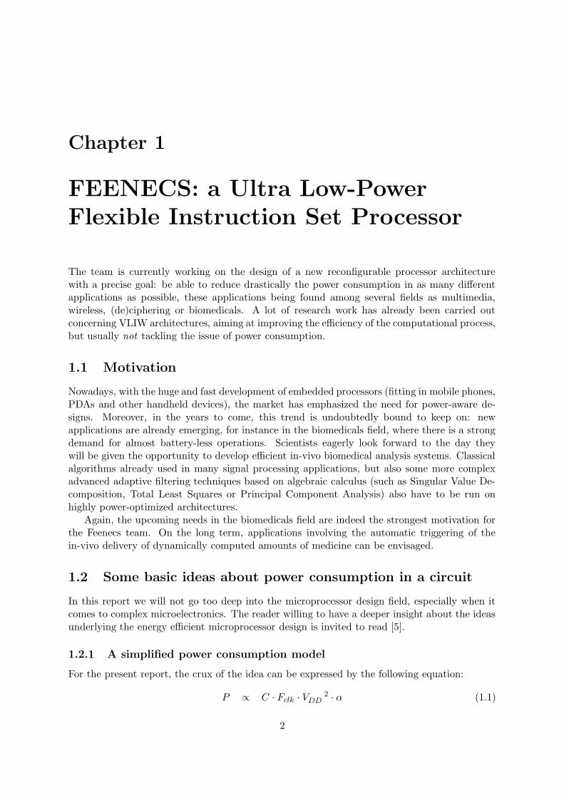
2.1 The Feenecs layout
In all the present part, we will only focus on a part of the Feenecs proposed architecture,composed of two very wide registers, two multiplexers, one adder and one demultiplexer. Theorganization of the layout is shown in figure 2.1.
Throughout my experiments, the dp datapath width in fig. 2.1 varied from 32 to 128 bits.For clarity reasons, some 1-bit control signals have not been represented in fig. 2.1, but thedifferent modules we used can fe found in appendix A.
2.2 Shaping the modules and placing their pins
2.2.1 Motivation
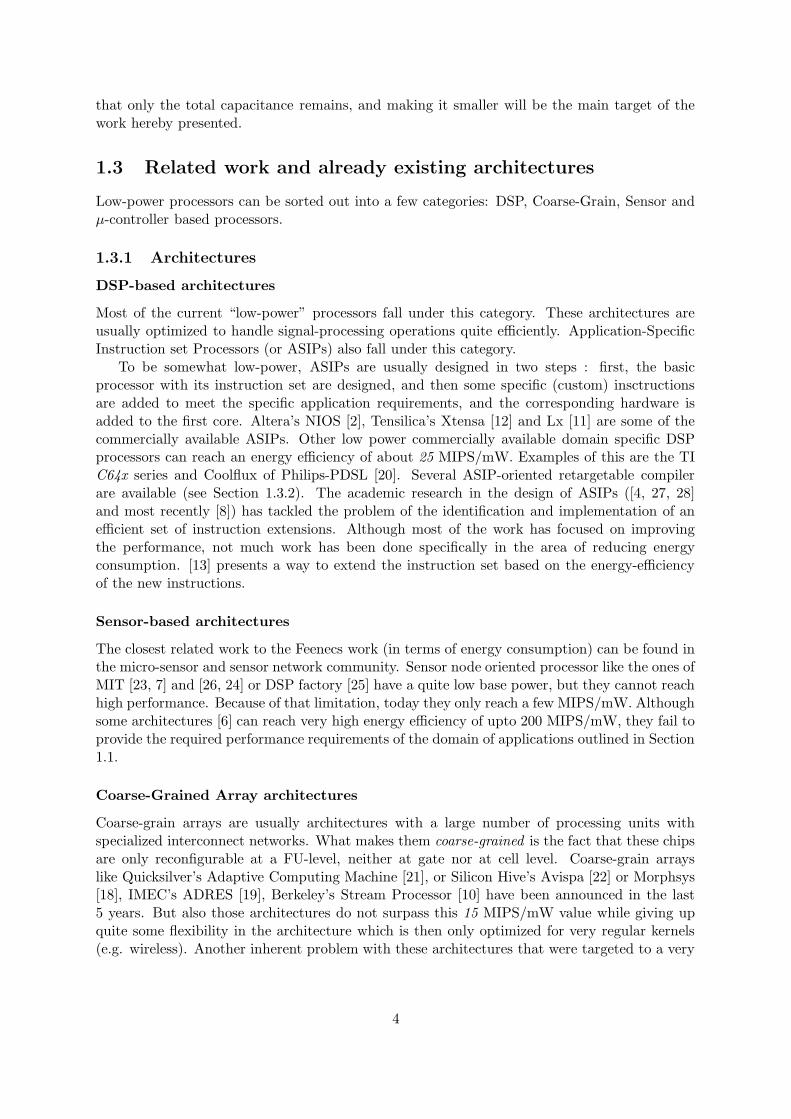
It is a relevant move to tackle the shape and pin placement of the different modules we use(adder, register files, etc). In effect, if the designer is allowed to shape its modules and specifythe pin locations on their side, he will be enabled to use smaller interconnect nets in thefloorplanning stage. Remember that large interconnect nets increase the capacitance of thecircuit and hence its power consumption. To illustrate such an effect, you can see differentresults I obtained in the floorplanning tool, depending on the modules I fed it with, in fig. 2.2,2.3 and finally 2.4.
2.2.2 Assessing the in-module consumption overhead due to form factor and
pin placement
Now that we have made clear that if we can shape the modules and place the pins consistentlyin regard to the modules interconnects, we are bound to save a lot of energy in the interconnectnets, we need to know whether the cost in terms of internal module capacitance is prohibitiveor not. We used the UMCE cells in their 130 nm, worst-case, 1.08V flavour.To gather accurate results, we designed some modules with Physical Compiler, forcing them to
9
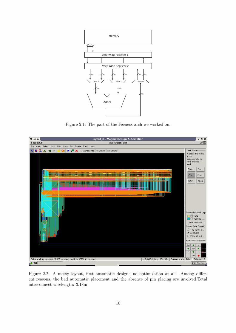
Figure 2.1: The part of the Feenecs arch we worked on.
Figure 2.2: A messy layout, first automatic design: no optimization at all. Among differ-ent reasons, the bad automatic placement and the absence of pin placing are involved.Totalinterconnect wirelength: 3.18m
10
Figure 2.3: An intermediate layout. This one is partially optimized, with the size of the modulesbeing modified to allow enough room for as direct wires as possible, and the pins placed moreaccurately. Still, horizontal congestion remains (e.g. in orange, layer 6), while this directionshouldn’t be significantly used.Total interconnect wirelength: 1.66m
11

Figure 2.4: Quite good a layout. With a correct placement of the pins, i.e. a placement awareof the position of the different modules, we have been able to eliminate efficiently the horizontalwires (even-numbered layers). The only remaining routing layers are the vertical ones (green& cyan, resp. layers 3 and 5), with very simple routes, almost intuitive. Total interconnectwirelength: 0.37m
12
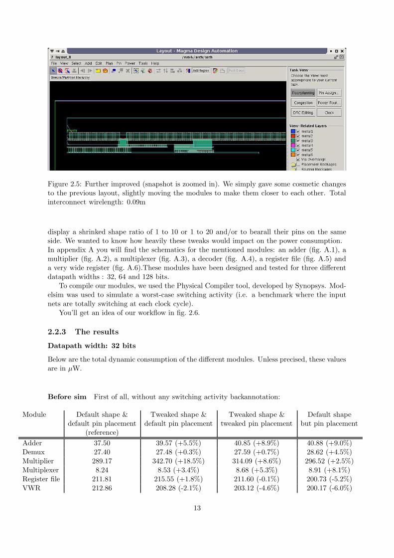
Figure 2.5: Further improved (snapshot is zoomed in). We simply gave some cosmetic changesto the previous layout, slightly moving the modules to make them closer to each other. Totalinterconnect wirelength: 0.09m
display a shrinked shape ratio of 1 to 10 or 1 to 20 and/or to bearall their pins on the sameside. We wanted to know how heavily these tweaks would impact on the power consumption.In appendix A you will find the schematics for the mentioned modules: an adder (fig. A.1), amultiplier (fig. A.2), a multiplexer (fig. A.3), a decoder (fig. A.4), a register file (fig. A.5) anda very wide register (fig. A.6).These modules have been designed and tested for three differentdatapath widths : 32, 64 and 128 bits.
To compile our modules, we used the Physical Compiler tool, developed by Synopsys. Mod-elsim was used to simulate a worst-case switching activity (i.e. a benchmark where the inputnets are totally switching at each clock cycle).
You’ll get an idea of our workflow in fig. 2.6.
2.2.3 The results
Datapath width: 32 bits
Below are the total dynamic consumption of the different modules. Unless precised, these valuesare in µW.
Before sim First of all, without any switching activity backannotation:
Module Default shape & Tweaked shape & Tweaked shape & Default shapedefault pin placement default pin placement tweaked pin placement but pin placement
(reference)
Adder 37.50 39.57 (+5.5%) 40.85 (+8.9%) 40.88 (+9.0%)Demux 27.40 27.48 (+0.3%) 27.59 (+0.7%) 28.62 (+4.5%)Multiplier 289.17 342.70 (+18.5%) 314.09 (+8.6%) 296.52 (+2.5%)Multiplexer 8.24 8.53 (+3.4%) 8.68 (+5.3%) 8.91 (+8.1%)Register file 211.81 215.55 (+1.8%) 211.60 (-0.1%) 200.73 (-5.2%)VWR 212.86 208.28 (-2.1%) 203.12 (-4.6%) 200.17 (-6.0%)
13

Figure 2.6: The flow through Physical Compiler and Modelsim
After sim Then, the above data corrected after backannotation by a switching activity sim-ulation done through Modelsim c© (worst-case switching, 20ns of clock period):
Module Default shape & Tweaked shape & Tweaked shape & Default shapedefault pin placement default pin placement tweaked pin placement but pin placement
(reference)
Adder 116.91 124.73 (+6.7%) 126.54 (+8.2%) 123.81 (+5.9%)Demux 98.35 98.69 (+0.4%) 98.99 (+0.7%) 102.49 (+4.2%)Multiplier 609.27 708.15 (+16.2%) 665.95 (+9.3%) 644.47 (+5.8%)Multiplexer 19.40 20.27 (+4.5%) 20.72 (+6.8%) 21.44 (+10.5%)Register file 702.80 694.26 (-1.2%) 688.64 (-2.0%) 702.91 (+0.0%)VWR to dp 470.76 473.70 (+0.6%) 461.20 (-2.0%) 467.17 (-0.8%)VWR to mem 659.34 653.89 (-0.8%) 636.63 (-3.4%) 650.01 (-1.4%)
Datapath width: 64 bits
Below are the total dynamic consumption of the different modules. Unless precised, these valuesare in µW.
Before sim First of all, without any switching activity backannotation:
14
Module Default shape & Tweaked shape & Tweaked shape & Default shapedefault pin placement default pin placement tweaked pin placement but pin placement
(reference)
Adder 84.78 84.16 (-0.7%) 89.26 (+5.3%) 94.21 (+11.1%)Demux 63.73 63.31 (-0.7%) 63.90 (+0.3%) 67.04 (+5.2%)Multiplier (mW) 1.19 1.25 (+5.8%) 1.25 (+5.5%) 1.25 (+5.1%)Multiplexer 16.72 16.51 (-1.3%) 16.88 (+1.0%) 19.23 (+15.0%)Register file 422.59 448.52 (+6.1%) 450.30 (+6.6%) 430.60 (+1.9%)VWR 432.15 447.69 (+3.6%) 437.07 (+1.1%) 426.75 (-1.3%)
After sim Then, the above data corrected after backannotation by a switching activity sim-ulation done through Modelsim c© (worst-case switching, 20ns of clock period):
Module Default shape & Tweaked shape & Tweaked shape & Default shapedefault pin placement default pin placement tweaked pin placement but pin placement
(reference)
Adder 271.26 272.26 (+0.4%) 286.29 (+5.5%) 287.77 (+6.1%)Demux 220.74 219.27 (-0.7%) 221.25 (+0.2%) 231.91 (+5.1%)Multiplier (mW) 2.26 2.41 (+6.7%) 2.40 (+6.5%) 2.41 (+6.9%)Multiplexer 39.53 38.87 (-1.7%) 40.02 (+1.2%) 47.26 (+19.5%)Register file (mW) 1.48 1.45 (-1.6%) 1.53 (+3.6%) 1.50 (+1.2%)VWR to dp 944.45 892.35 (-5.5%) 908.25 (-3.8%) 910.85 (-3.6%)VWR to mem (mW) 1.33 1.33 (+0.6%) 1.34 (+0.7%) 1.33 (+0.6%)
Datapath width: 128 bits
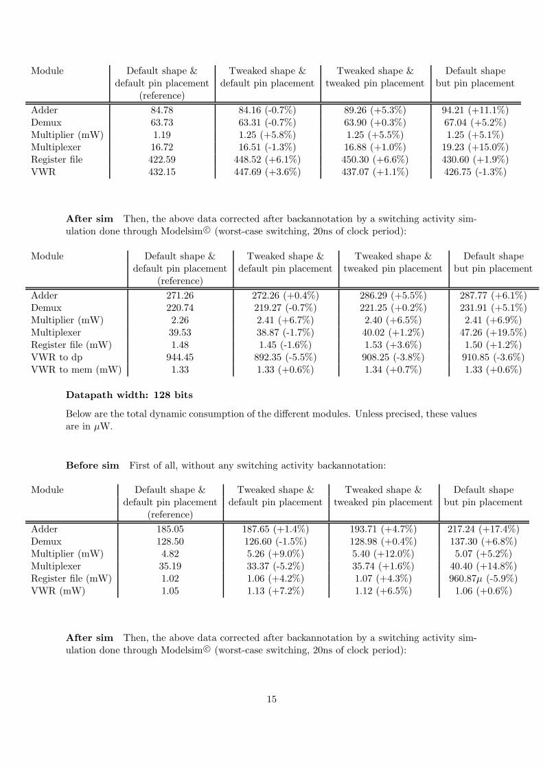
Below are the total dynamic consumption of the different modules. Unless precised, these valuesare in µW.
Before sim First of all, without any switching activity backannotation:
Module Default shape & Tweaked shape & Tweaked shape & Default shapedefault pin placement default pin placement tweaked pin placement but pin placement
(reference)
Adder 185.05 187.65 (+1.4%) 193.71 (+4.7%) 217.24 (+17.4%)Demux 128.50 126.60 (-1.5%) 128.98 (+0.4%) 137.30 (+6.8%)Multiplier (mW) 4.82 5.26 (+9.0%) 5.40 (+12.0%) 5.07 (+5.2%)Multiplexer 35.19 33.37 (-5.2%) 35.74 (+1.6%) 40.40 (+14.8%)Register file (mW) 1.02 1.06 (+4.2%) 1.07 (+4.3%) 960.87µ (-5.9%)VWR (mW) 1.05 1.13 (+7.2%) 1.12 (+6.5%) 1.06 (+0.6%)
After sim Then, the above data corrected after backannotation by a switching activity sim-ulation done through Modelsim c© (worst-case switching, 20ns of clock period):
15

Module Default shape & Tweaked shape & Tweaked shape & Default shapedefault pin placement default pin placement tweaked pin placement but pin placement
(reference)
Adder 612.93 635.27 (+3.6%) 642.59 (+4.8%) 670.37 (+9.4%)Demux 445.21 438.69 (-1.5%) 446.65 (+0.3%) 475.00 (+6.7%)Multiplier (mW) 8.54 9.14 (+7.0%) 9.77 (+14.4%) 9.17 (+7.4%)Multiplexer 83.55 78.02 (-6.6%) 85.25 (+2.0%) 99.51 (+19.1%)Register file (mW) 3.06 3.00 (-1.9%) 3.02 (-1.1%) 3.09 (+1.1%)VWR to dp (mW) 1.97 2.03 (+2.9%) 1.95 (-1.1%) 2.06 (+4.6%)VWR to mem (mW) 2.87 2.92 (+1.8%) 2.91 (+1.4%) 2.88 (+0.5%)
Roughly speaking, as shown in fig. 2.7, the consumption scales exponentially with the widthof the datapath, but with exponentiation factors which vary from one module to another: thegrowth is linear (k = 1) for the adders, multiplexers and demultiplexers, while it’s quadratic(k = 2) in the case of the multiplier. Concerning the register files and very wide registers, sucha pattern (power = a · sizek) might apply, but as for now there is no widespread literature onthe subject, we will not insist on that point (that was not the main field of exploration of myintern, anyway).
8
16
32
64
128
256
512
1024
2048
4096
8192
128 bits64 bits32 bits
Pow
er c
onsu
mpt
ion
($m
u$W
)
Datapath width
AdderDemux
MultMuxRF
VWRDemux-fit: a= 0.74 ; k= 1.06
Mult-fit: a= 0.27 ; k= 2.02RF-fit: a= 2.93 ; k= 1.21
Figure 2.7: How consumption scales with bitsize (curve-fitting values correspond to the formulapower = a . sizek̂)
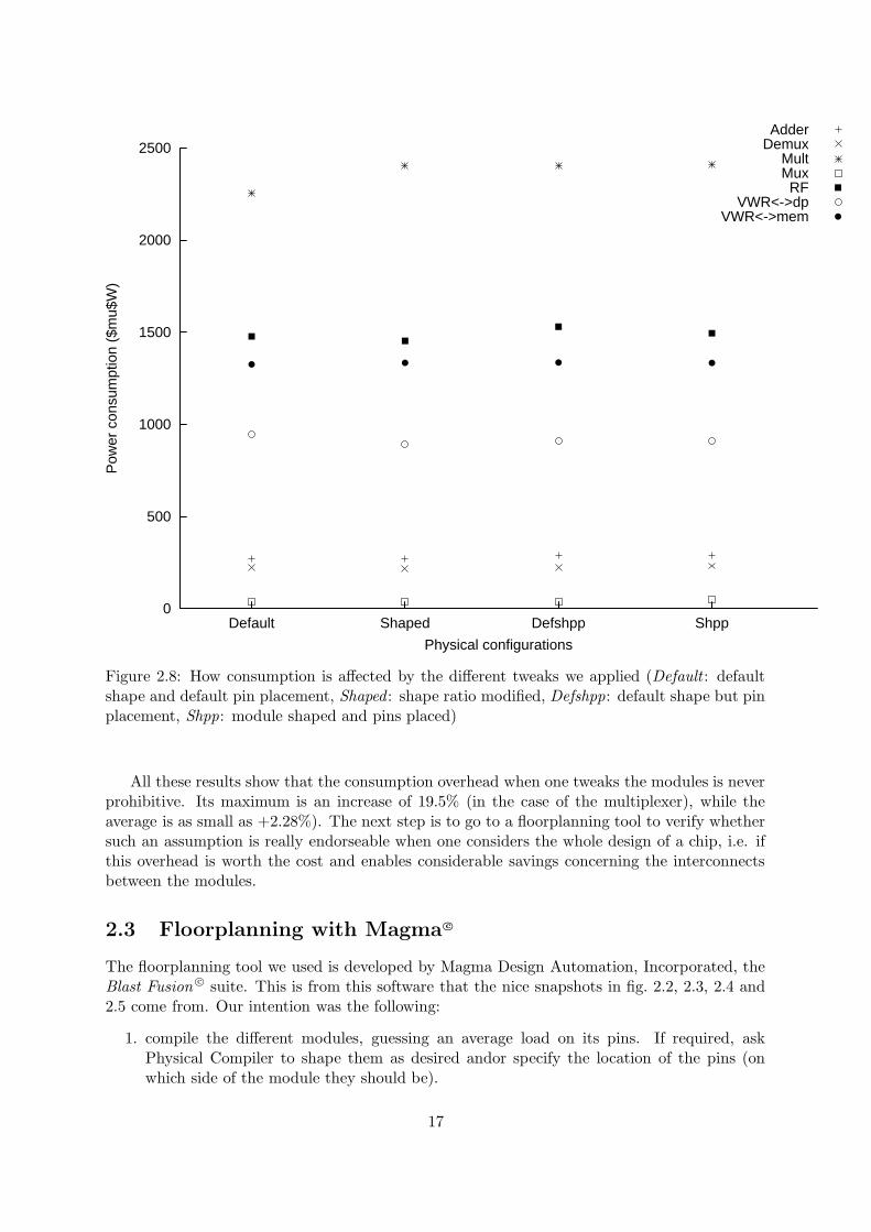
Concerning the way power consumption is affected by the shaping and pin placing, pleaserefer to fig. 2.8
16
0
500
1000
1500
2000
2500
ShppDefshppShapedDefault
Pow
er c
onsu
mpt
ion
($m
u$W
)
Physical configurations
AdderDemux
MultMuxRF
VWR<->dpVWR<->mem
Figure 2.8: How consumption is affected by the different tweaks we applied (Default : defaultshape and default pin placement, Shaped : shape ratio modified, Defshpp: default shape but pinplacement, Shpp: module shaped and pins placed)
All these results show that the consumption overhead when one tweaks the modules is neverprohibitive. Its maximum is an increase of 19.5% (in the case of the multiplexer), while theaverage is as small as +2.28%). The next step is to go to a floorplanning tool to verify whethersuch an assumption is really endorseable when one considers the whole design of a chip, i.e. ifthis overhead is worth the cost and enables considerable savings concerning the interconnectsbetween the modules.
2.3 Floorplanning with Magma c©
The floorplanning tool we used is developed by Magma Design Automation, Incorporated, theBlast Fusion c© suite. This is from this software that the nice snapshots in fig. 2.2, 2.3, 2.4 and2.5 come from. Our intention was the following:
1. compile the different modules, guessing an average load on its pins. If required, askPhysical Compiler to shape them as desired andor specify the location of the pins (onwhich side of the module they should be).
17

2. do the floorplanning by hand in Magma, using the modules we designed in PhysicalCompiler
3. extract the interconnect net capacitances of the obtained floorplan
4. put these back into the Physical Compiler tool so that it could update, in each module,the loads that its output pins have to drive.
5. compile the modules again, to take into account possible changes in the low-level designdue to the new laods to drive
6. report for the new power consumption of the separate modules
The idea behind this new workflow is that a module whose output pins will have to drivenets of a small capacitance will use small output buffers, which will not drain a lot of energy.Increasing the output load will entail the need for bigger output buffer, which will consumemore energy.
So that if we want to get consistent numbers concerning the power consumption of theseparate modules, we necessarily have to take into account the loads of the interconnect nets,that we obtain from the floorplanning tool. This accounts for the tight interplay betweenplace$route and floorplanning tools.
This new workflow, described in fig. 2.9, involved quite a lot of scripting work to parse thedifferent files used to bring the information from one tool to another. As a geek, I used thepowerful Unix tools sed and awk
1, but also some Tcl.
During my stay I wrote a short tutorial about these tools I developed. It describes in moredetail the work I carried out with Physical Compiler and Magma. As for now this is a documentinternal to IMEC, I will provide indivudual copies on request.
2.4 A second series of results
To be able to assess correctly the influence of module shaping and pin placement, we neededa flat design to be considered as a reference. By “flat design”, we mean a design where thecombination of the different .vhd files giving the code of the different modules have been fedto the P&R tool for compilation, so that the remaining job for the floorplanner was to connectthis design to the memory.
We then tried to see whether the overhead cost paid during the ”intelligent module design”phase could be cancelled in the floorplanning phase. Facing some weird non-technical issuesrelated to the tool itself (namely Synopsys’ Physical Compiler, which sometimes behaved oddlywhen asked to report about the power consumption), we chose to stick to the net capacitances.We remind the reader that under eqn. 1.1, total net capacitances are a good means to evaluatethe power consumption (provided that the clock frequency does not change, of course: thefollowing results are all with 500MHz clocks).
1About the utmost powerful Awk language, I strongly recommend the old but still extremely useful book byits inventors, [1].
18

Figure 2.9: The global flow through Physical Compiler, Magma and Modelsim.The arrows labelled with slanted fonts correspond to some commands included in the used tools,while upright font labels refers to one of my scripts.
19

Figure 2.10: Datapath is 96 bits, clock is 500MHz
The experiments we made following the workflow described in the previous section ledus to some interesting results: as constaraining more and more the design could, in certaincases, worsen the power consumption figures, finally when the shape and pin placement werecorrectly coordinated, we undoubtedly managed to lower the power consumption of the design(see fig. 2.10).
20

Chapter 3
The Software Toolchain: Scheduling,
Tiling & Assignment in a
Trimaran-Based Approach
As explained in section 1.3.2, a good architecture has to come along with a good compiler. Thisis the baseline that sparked in the team the interest for the customizable software toolchaincalled Trimaran, and developed in different locations in the US, though mainly at New YorkUniversity (see www.trimaran.org). It is not optimized in regard with the power consumptionof the resulting schedule, but is highly customizable, and this features ranks it as one of thebest academic tools for Custom Instruction Set Processors exploration.
3.1 Trimaran, a complete compiler and simulator toolchain
Basically, Trimaran works as shown in fig.3.1.
It is a powerful tool to compile some C code and get a schedule where the constraints ofthe architecture (e.g. latency time of an operation, number and type of resources, etc) arecorrectly taken into acount. The user is then enabled to view many reports about the level ofparallelisation reached, the most time-consuming loops, the power consumption (calculation isonly based on some assumptions that sometimes prove not accurate), etc.
3.2 My work
My work on Trimaran essentially consisted in merging two branches of its development inthe SMART team, adding support for instruction clustering in a branch already includinginstruction set customization features. I modified here and there the source files related to theparsing of the machine description files, the Impact and the Elcor steps.
21

Figure 3.1: The Trimaran software toolchain
22

Chapter 4
Afterword
Many academic papers present new architectural ideas and bring under the lights some pro-posed design, almost none tackles the issue of the importance of low-level design on the powerconsumption of the resulting chip. The work about Feenecs is about bringing together high-levelconcepts as instruction clustering, but also silicon-level issues, aiming at the design of an ultra-low power customizable processor. My small contribution is part of this framework, underlyingthe importance of physical aspects.
About the interesting work still to do – yes, usually there is always a lot more that can bedone –, I personally think that the problem of tiling, i.e. finding how to detect in a high-levelprogramming code (C or its offsprings, for instance), when it is relevant to compile it to a certainfunctional unit seems highly interesting. Also, the codesign of a chip based on the software itwill have to run, the definition of an appropriate set of instruction able to minimize the loopexecution time or power consumption is still to be explored.
I enjoyed my stay in IMEC quite a lot. I learned about new tools, and it was my firstcontact with a world sitting across the boundary between academic research and industrialdevelopment. These three months have been intense and productive.
Also, I met with a young research team, made out of brilliant and funny people: MuraliJayapala, Andy Lambrechts, Praveen Raghavan and Guillermo Talavera. Last but not least, Iwould like to thank Prof. Francky Catthoor, who made it possible. We also spent a thick bunchof hours together on our bike saddles through Belgium. Some of those hours made me blissfullyhappy.
23
Appendix A
The different modules written and
used
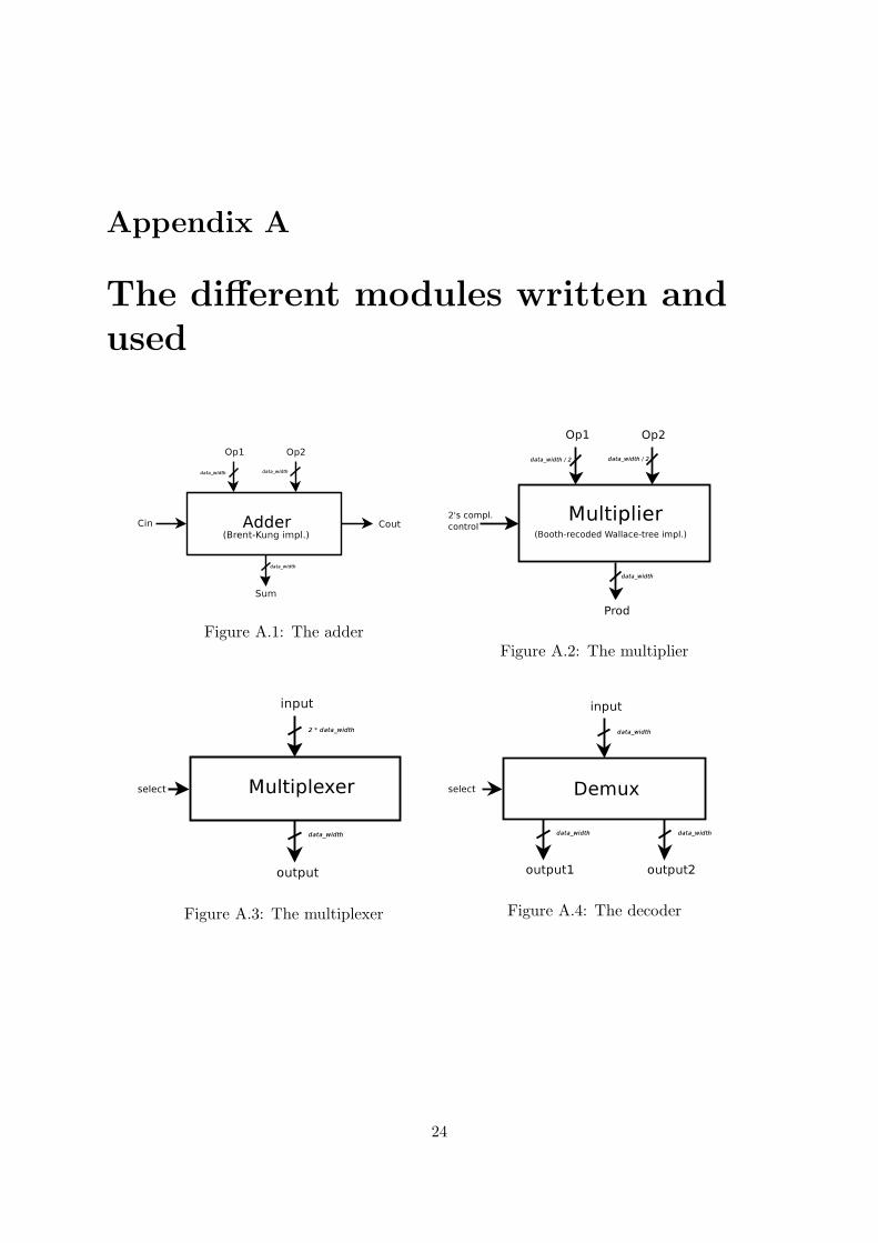
Figure A.1: The adderFigure A.2: The multiplier
Figure A.3: The multiplexer Figure A.4: The decoder
24
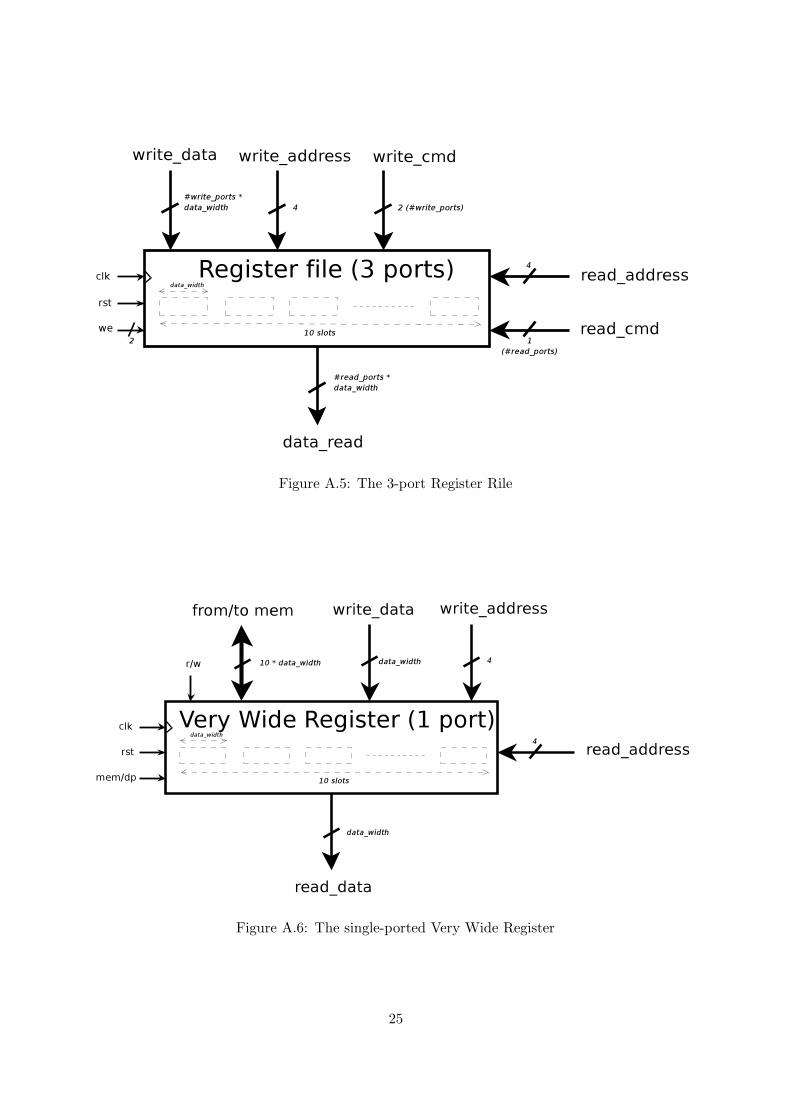
Figure A.5: The 3-port Register Rile
Figure A.6: The single-ported Very Wide Register
25

Bibliography
[1] A. V. Aho, B. W. Kernighan, and P. J. Weinberger. The AWK Programming Language.Addison-Wesley, 1988.
[2] Altera. Nios embedded processor system developement. Inhttp://www.altera.com/products/ip/processors/nios.
[3] J. Ayala, M. Vallejo, A. Veidenbaum, and C. Lopez. Energy aware register file implemen-tation through intruction precode. In Proc of ASAP, September 2003.
[4] P. Biswas, V. Choudhary, K. Atasu, L. Pozzi, P. Ienne, and N. Dutt. Introduction of localmemory elements in instruction set extensions. In Proc of DAC, pages 729–734, June 2004.
[5] T. D. Burd and R. W. Brodersen. Energy efficient microprocessor design. Kluwer AcademicPublishers, 2002.
[6] B. H. Calhoun and A. Chandrakasan. Ultra-dynamic voltage scaling using sub-thresholdoperation and local voltage dithering in 90nm cmos. In Proc of ISSCC, February 2005.
[7] A. Chandrakasan, R. Min, M. Bhardwaj, S.-H. Cho, and A. Wang. Power aware wirelessmicrosensor systems. In Keynote address at ESSCIRC, 2002.
[8] N. T. Clark, H. Zhong, and S. A. Mahlke. Automated custom instruction generationfor domain-specific processor acceleration. In IEEE Transactions on Computers, vol. 54,no. 10, pages 1258–1270, October 2005.
[9] Coware. Lisatek: Automated embedded processor de-sign and software development tool generation. Inwww.coware.com/pls/cust portal/URL/PAGE/PRODUCTSOLS/PRODUCTSBASEPAGE/LISATEKPRODUCTS.
[10] W. Dally and U. K. et. al. Stream processors: Programmability with efficiency. In QueueFocus DSP, 2004.
[11] P. F. et. al. Lx: a technology platform for customizable vliw embedded processing. In Procof ISCA, 2000.
[12] R. Gonzalez. Xtensa: A configurable and extensible processor. In IEEE Micro, volume20(2), 2002.
[13] K. C. J. Lee and N. Dutt. Energy-efficient instruction set synthesis for application-specificprocessors. In Proc of ISLPED, August 2003.
[14] N. Kim and T. Mudge. The microarchitecture of a low power register file. In Proc ofISLPED, pages 384–389, 2003.
26

[15] D. Lanneer, J. Praet, A. Kilfi, K. Schoofs, and W. Geurts. Chess: Retargetable codegeneration for embedded dsp processors. In Code Generation for Embedded Processors,pages 85–102, 1995.
[16] V. S. Lapinskii, M. F. Jacome, and G. A. de Vecina. Application-specific clustered vliwdatapaths: Early exploration of a parameterized design space. In IEEE Transactions onComputer-Aided Design of Integrated Circuits and Systems, Vol. 21, August 2002.
[17] V. S. Lapinskii, M. F. Jacome, and G. A. de Vecina. Cluster assignment for high-performance embedded vliw processors. In ACM Transactions on Design Automation ofElectronic Systems, Vol.7, July 2002.
[18] G. Lu, H. Singh, M. Lee, N. Bagherzadeh, F. Kurdahi, and E. Filho. The morposys parallelreconfigurable system. In Proc of Euro-Par, 1999.
[19] B. Mei, S. Vernalde, D. Verkest, H. D. Man, and R. Lauwereins. Adres: An architecturewith tightly coupled vliw processor and coarse-grained reconfigurable matrix. In Proc ofFPL, 2003.
[20] P. PDSL. Coolflux dsp. In http://www.coolfluxdsp.com.
[21] Quicksilver. Quick adaptive computing machine (adapt2400). In http://www.qstech.com.
[22] P. Research. Philips siliconhive avispa accelerator. Inhttp://www.research.philips.com/technologies/syst softw/siliconhive/.
[23] S. Rhee and S. Liu. An ultra-low power, self-organizing wireless network and its applica-tions to non-invasive biomedical instrumentation. In IEEE Symposium Wired and WirelessCommunication, March 2002.
[24] A. Savvides and M. Srivatsava. A distributed computation platform for wireless embeddedsensing. In Proc of ICCD, 2003.
[25] A. Semiconductor. Toccata plus flexible dsp. Inhttp://www.amis.com/products/dsp/toccata plus.html.
[26] J. Wong, S. Megerian, and M. Potkonjak. Design techniques for sensor appliances: Foun-dations and light compass case study. In Proc of DAC, 2003.
[27] P. Yu and T. Mitra. Characterizing embedded applications for instruction set extensibleprocessors. In Proc of DAC, pages 723–728, June 2004.
[28] P. Yu and T. Mitra. Scalable instructions identification for instruction-set extensible pro-cessors. In Proc of CASES, September 2004.
27