Embed Size (px)
Citation preview

Wireless surface stimulator
Gergely Andor Maksay
August 21, 2009
Matriculation number: 0803879
Academic year 2008/2009
�rst supervisor: Dr. Bernd Porr
second supervisor: Dr. Khaled Elgaid

Abstract
Functional electrical stimulation (FES) is the stimulation of peripheralnerves on innervated paralysed muscle groups with the purpose of facili-tating a functional movement. It is excercised in particularly to aid therehabilitation of people with paraplegia. For that application, a low cost,portable, battery powered neuromuscular surface stimulation system wasdeveloped and implemented, which is capable of delivering high voltage,constant current controlled faradic pulse trains through surface electrodes.The stimulation waveform is �exibly adjustable by the current amplitude( 0-100 mA ), the pulse width ( 40-500 µs ), and the repetition frequencyof pulses ( 25-300 Hz ). These parameters can be remotely con�guredfrom a personal computer over a wireless sub 1 GHz radio frequency link.The entire system consists of the stimulator board, an interface boardresponsible for the wireless transmission of commands from the PC, andthe Matlab software which interacts with the operator through a graphi-cal user interface. The stimulator is microcontroller based and the outputstage consists of a minimalistic modi�ed boost converter. Special e�ortswere made to optimise the device for low power consumption. Besidesit's intended application �eld the system is apt to be universally used fortherapy and research.
ii

Contents
1 Introduction 1
2 Neuromuscular stimulation 22.1 Nerve and muscle cells . . . . . . . . . . . . . . . . . . . . . . . . 22.2 Electrical stimulation in practice . . . . . . . . . . . . . . . . . . 22.3 Functional electrical stimulation (FES) . . . . . . . . . . . . . . . 42.4 Impedance model of skin . . . . . . . . . . . . . . . . . . . . . . . 5
3 Stimulator output stage 73.1 Boost regulators . . . . . . . . . . . . . . . . . . . . . . . . . . . 73.2 Output stage . . . . . . . . . . . . . . . . . . . . . . . . . . . . . 93.3 Selection of circuit components . . . . . . . . . . . . . . . . . . . 173.4 Current consumption . . . . . . . . . . . . . . . . . . . . . . . . . 183.5 Closed loop control . . . . . . . . . . . . . . . . . . . . . . . . . . 18
4 Wireless communication 204.1 CC1000 . . . . . . . . . . . . . . . . . . . . . . . . . . . . . . . . 204.2 Antenna design . . . . . . . . . . . . . . . . . . . . . . . . . . . . 24
5 Overall system description 265.1 Wireless stimulator . . . . . . . . . . . . . . . . . . . . . . . . . . 26
5.1.1 Hardware description . . . . . . . . . . . . . . . . . . . . 265.1.2 Software description . . . . . . . . . . . . . . . . . . . . . 28
5.2 RS232/Wireless interface . . . . . . . . . . . . . . . . . . . . . . 365.2.1 Hardware description . . . . . . . . . . . . . . . . . . . . 365.2.2 Software description . . . . . . . . . . . . . . . . . . . . . 37
6 Performance analysis 41
7 User's guide 46
8 Future development plans 49
9 Conclusion 51
iii

List of Figures
1 Waveform of biphasic pulses and nomenclature of pulse properties 42 Equivalent electrical model of electrodes, skin and tissue . . . . 63 Boost regulator . . . . . . . . . . . . . . . . . . . . . . . . . . . . 74 Boost regulator, while transistor is on . . . . . . . . . . . . . . . 85 Boost regulator, while transistor is o� . . . . . . . . . . . . . . . 86 Stimulator output stage . . . . . . . . . . . . . . . . . . . . . . . 97 Inductor current and voltage in a boost regulator ( no load ) . . 128 Spice simulations of rising output voltage, if boost converter's
load is removed . . . . . . . . . . . . . . . . . . . . . . . . . . . . 149 Spice simulation of output stage . . . . . . . . . . . . . . . . . . 1610 Block diagram explaining the closed loop control of the boost
converter . . . . . . . . . . . . . . . . . . . . . . . . . . . . . . . 1911 The complete output stage of the stimulator . . . . . . . . . . . . 1912 Block diagram of the CC1000 [21], with permission of TI . . . . . 2213 Transmitted power spectrum of the FSKmodulated system, rough
estimation . . . . . . . . . . . . . . . . . . . . . . . . . . . . . . . 2314 Synchronous Manchester encoding [21], with permission of TI . . 2415 The wireless stimulation system . . . . . . . . . . . . . . . . . . . 2616 Block diagram of wireless stimulator . . . . . . . . . . . . . . . . 2717 Functional block diagram of the MSP430F2122 microcontroller[17],
with permission of TI . . . . . . . . . . . . . . . . . . . . . . . . 2718 Main() function of wireless stimulation software . . . . . . . . . 3019 PWM generation of Timer_A1 and Timer_A2 . . . . . . . . . . 3120 Algorithm for implementing the digital controller . . . . . . . . . 3321 Flowchart of the wireless communication handling . . . . . . . . 3522 Block diagram of RS232/Wireless interfacing board . . . . . . . . 3623 Flowchart for Main() function of Interfacing board . . . . . . . . 3724 Flowchart of external interrupt handling in the main loop . . . . 3825 Timer_A0 ISR for button polling . . . . . . . . . . . . . . . . . . 3926 The USCI interrupt routine in main loop . . . . . . . . . . . . . 4027 Oscilloscope measurements of stimulator output pulses . . . . . . 4428 Front view image of the boards . . . . . . . . . . . . . . . . . . . 4629 Matlab program's graphical user interface . . . . . . . . . . . . . 47
iv

List of Tables
1 Technical details of RehaStim stimulator . . . . . . . . . . . . . . 12 Typical current consumption of the CC1000 [21] . . . . . . . . . 203 Packet format . . . . . . . . . . . . . . . . . . . . . . . . . . . . 344 Data Field of 'Update' packets . . . . . . . . . . . . . . . . . . . 345 Source �les of the software . . . . . . . . . . . . . . . . . . . . . . 367 Estimated power consumption of the stimulator . . . . . . . . . . 428 Characteristics of the wireless stimulator in comparison with the
speci�ed technical details of RehaStim[2]. . . . . . . . . . . . . . 43
v

List of Abbreviations
AC Alternating currentADC Analog-digital converterBER Bit error rateBJT Bipolar junction transistorCMOS Complementary metal�oxide�semiconductorCPU Central processing unitDC Direct currentDCO Digitally Controlled OscillatorEEG ElectroencephalogramEMG ElectromyogramENG ElectroneurogramFES Functional electrical stimulationFET Flash emulation toolFSK Frequency shift keyingGCC GNU compiler collectionGDB GNU debuggerGPIO General purpose input/outputGUI Graphical user interfaceIC Integrated circuitIF Intermediate frequencyISM Industrial, Scienti�c and MedicalISR Interrupt service routineITU International Telecommunication UnionJTAG Joint Test Action GroupLED Light emitting diodeLNA Low noise ampli�erLPF Low pass �lterMCU Microcontroller unitMOSFET Metal�oxide�semiconductor Field-e�ect transistorNRZ Non return to zeroPA Power ampli�erPC Personal computerPCB Printed circuit boardPD Phase detectorPD Power down modePLL Phase locked loopPWM Pulse width modulationRAM Random access memoryRISC Reduced instruction set computing
vi

SMPS Switched mode power supplyTACCR Timer_A capture/compare registerTAR Timer_A registerTI Texas InstrumentsTSSOP Thin-shrink Small Outline PackageUART Universal asynchronous receiver/transmitterUHF Ultra high frequencyUSB Universal serial busUSCI Universal serial communication interfaceVCO Voltage controlled oscillator
vii
1 Introduction
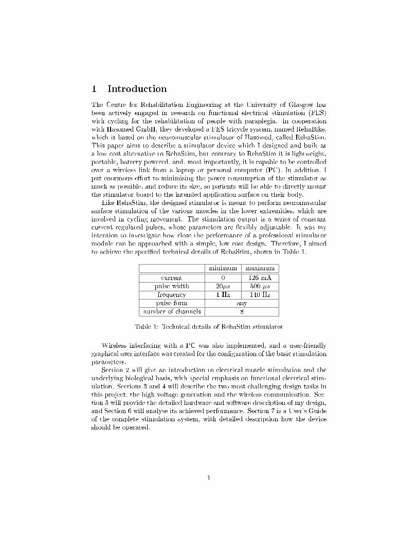
The Centre for Rehabilitation Engineering at the University of Glasgow hasbeen actively engaged in research on functional electrical stimulation (FES)with cycling for the rehabilitation of people with paraplegia. In cooperationwith Hasomed GmbH, they developed a FES tricycle system, named RehaBike,which is based on the neuromuscular stimulator of Hasomed, called RehaStim.This paper aims to describe a stimulator device which I designed and built asa low cost alternative to RehaStim, but contrary to RehaStim it is lightweight,portable, battery powered, and, most importantly, it is capable to be controlledover a wireless link from a laptop or personal computer (PC). In addition, Iput enormous e�ort to minimising the power consumption of the stimulator asmuch as possible, and reduce its size, so patients will be able to directly mountthe stimulator board to the intended application surface on their body.
Like RehaStim, the designed stimulator is meant to perform neuromuscularsurface stimulation of the various muscles in the lower extremities, which areinvolved in cycling movement. The stimulation output is a series of constantcurrent regulated pulses, whose parameters are �exibly adjustable. It was myintention to investigate how close the performance of a professional stimulatormodule can be approached with a simple, low cost design. Therefore, I aimedto achieve the speci�ed technical details of RehaStim, shown in Table 1.
minimum maximum
current 0 126 mApulse width 20µs 500 µsfrequency 1 Hz 140 Hzpulse form any
number of channels 8
Table 1: Technical details of RehaStim stimulator
Wireless interfacing with a PC was also implemented, and a user-friendlygraphical user interface was created for the con�guration of the basic stimulationparameters.
Section 2 will give an introduction to electrical muscle stimulation and theunderlying biological basis, with special emphasis on functional electrical stim-ulation. Sections 3 and 4 will describe the two most challenging design tasks inthis project, the high voltage generation and the wireless communication. Sec-tion 5 will provide the detailed hardware and software description of my design,and Section 6 will analyse its achieved performance. Section 7 is a User's Guideof the complete stimulation system, with detailed description how the deviceshould be operated.
1

2 Neuromuscular stimulation
A long time elapsed since Luigi Galvani �rst discovered that frog muscles twitchby the application of electrical current. Today, electrotherapy became a stan-dard practice in medicine. It is used to cure neurological diseases, facilitatewound ailment, recover muscle functions after spinal cord injury, just to namea few. This section will discuss the basic concepts of electrical stimulation witha brief introduction to the biology of nerve and muscle cells, which is utterlynecessary to understand the further discussion in this section. After then, func-tional electrical stimulation, the intended application �eld of the subject devicewill be introduced, and the most important speci�cations of a common stimu-lator will be examined. Most of the presented information was gathered from[3, 4, 5], unless otherwise noted.
2.1 Nerve and muscle cells
Cells contain lower concentration of positive cations, than the surrounding ex-tracellular �uid, which causes a potential di�erence between the two sides of thecell membrane. The electronegative voltage of cells is called resting potential,and it is sustained by active biochemical and electrostatical processes. It is pos-sible to reverse this voltage in nerve cells ( neurons) and muscle cells (muscle�bres ) by depolarising the cell membrane with su�ciently intense electric �eld( current ) of su�cient duration. The excitation of the cell membrane producesan action potential which propagates along the lengthy nerve �bre (the axon)to the subsequent nerve or muscle cell. The links between muscle �bres andneurons are called motor units, which consist of the neurons attached to severalparallel muscle �bres. An action potential on a motor unit causes a twitch onall corresponding muscle �bres. There are many motor units in a muscle. Theyactivate with a relative phase shift and the resulting �ring pattern determinesthe smooth muscular movement[3, 4].
2.2 Electrical stimulation in practice
The above described physiological process is natural, but the same e�ect canbe triggered arti�cially by applying an electrical pulse train through the tissue.The induced current causes electric �eld along its path, which depolarises themembrane of motor units. The result is a twitch of the muscle. The stimula-tion of innervated tissue is called neuromuscular stimulation, which will be theintended application of the device presented in this document. It is also possi-ble to stimulate denervated muscles directly, although the threshold charge foractivating muscle �bres is signi�cantly larger than that of neurons, thus opin-ions vary about its e�ectiveness. This stimulation technique is called electricalmuscular stimulation.
There are various ways how stimulation electrodes can be applied. The sim-plest and cheapest method is to place surface electrodes on the skin noninva-sively. This technique, called transcutaneous stimulation, has the disadvantage,
2

that the skin-electrode interface signi�cantly heightens the impedance of thetotal system to be stimulated. Furthermore, a trained therapist is needed toaccurately apply the electrode to the intended area. In order to achieve maximalcontraction force, one electrode ( called active electrode, typically the anode )must be placed over the motor points, where the largest concentration of motorunits is situated. The other electrode ( return electrode ) is typically placed onthe muscle belly[3]. Transcutaneuos stimulation might also be hurtful for pa-tients as pain receptors are also stimulated. Alternative to surface electrodes arethe invasive percutaneous and implanted electrodes, about which please refer to[5].
There are many aspects of characterising neuromuscular stimulators. Theycan be portable or line powered, high voltage or low voltage, their output can beconstant voltage or constant current regulated, but maybe their most importantfeature is the waveform they produce.
There is still active research to �nd the optimal waveform of the appliedcurrent.
In order to stimulate denervated muscle, usually long ( 100 ms ) galvanic (interrupted ) DC pulses are used.
Other applications use high frequency interferential or tone burst AC pulses.Neuromuscular stimulation, and in particular functional electrical stimula-
tion, rather uses a low frequency (<100 Hz) faradic pulse train, which can becharacterised with the amplitude of pulses, the repetition frequency of pulsesand the pulse duration[3]. Because the electrode-tissue interface has capacitiveproperties, every delivered pulse builds up charge in the tissue which can bepotentially harmful, especially in case of implanted electrodes. To prevent this,sometimes another pulse with opposite polarity ( called reverse pulse ) is in-duced to balance the net charge. This type of stimulation is called biphasic,while an unipolar pulse train is referred to as monophasic. Biphasic stimulationis generally safer, but the threshold current for activating muscle movementwill be higher, as the induced electric �eld will be more localised. The solutionis the application of pseudomorphic biphasic pulses, which are prolonged andhave lower amplitudes, but still deliver the same amount of charge[6]. Figure 1displays a biphasic pulse with the de�nition of the pulse parameter terminologythat will be used in the rest of this paper.
The strength of muscle contraction can be controlled by the parameters ofstimulation[5].
The current amplitude and pulse duration controls the total amount of in-jected charge. Increasing either of these parameters will result in larger electric�eld, more and more motoneurons ( motor units ) will be a�ected, increas-ing number of muscle �bres twitch which contributes to the total force of thecontraction ( this e�ect is know as spatial summation ).
If the time interval of the applied stimuli is shorter than the duration ofthe twitch, then the exerted tension will rise additively, until the upper limit( tetanus ) of contraction is reached ( cumulative e�ect of stimulus repetitionis known as temporal summation ). For this reason, the stimulation frequencymust be higher than the so called fusion frequency for a smooth contraction,
3

Figure 1: Waveform of biphasic pulses and nomenclature of pulse propertiesNote that pulse widths are unrealistically exaggerated for better demonstrationreasons
otherwise the response will be a series of twitches[4]. It must be noted, thatincreasing stimulation frequency also increases the rate of muscle fatigue. Forthese reasons, the repetition frequency of pulses is usually higher than 12 Hz,but rarely exceeds 100 Hz[5].
Muscles come in di�erent size and shape, which also determines the max-imal force, susceptibility to fatigue, and the time for a twitch. Thus the pa-rameters of stimulation must be adapted to muscle type. According to today'ssuggested practice slow muscles are trained with weaker, but sustained tonicactivation, and fast muscles are rather trained with shorter, but more intensephasic stimuli[3].
2.3 Functional electrical stimulation (FES)
Functional electrical stimulation is the stimulation of the peripheral nerves withthe purpose of facilitating some kind of functional movement. It must be dis-tinguished from therapeutic electrical stimulation, which aims to improve tissuehealth and permanently restore sensory functions, and the stimulation is notnecessarily accompanied by actual movement[3, 5]. It was already mentioned,that neuromuscular stimulation is only used to stimulate innervated healthymuscles. Because of this, most of the patients bene�tting from this technologytypically su�ered spinal cord or head injury, stroke, cerebral palsy, or multiplesclerosis.
Every movement involves the contraction of a variety of muscles, and eachmuscle moves as the result of a very complex �ring pattern of motor units.There is still signi�cant ongoing research toward the arti�cial imitation of nat-ural muscle movement. Neuroprostheses1 have been successfully tested for theupper and lower extremities, the bowels, and the respiratory system, but even
1FES devices used for substituting a neurological function[5]
4

bladder control of patients could be recovered with FES. Several systems un-derwent clinical trials and are now available as commercial products. Todaythe main concentration area of research is the closed loop control of stimulationwith feedback from a combination of biopotentials, including nerves ( ENG,electroneurogram ), muscles (EMG), and the brain(EEG). Others are applyingimplanted stimulators powered and controlled by inductive links, and connectingneuroprostheses in a network[5].
FES cycling
The Centre for Rehabilitation Engineering at the University of Glasgow andHasomed GmbH. developed a tricycle system allowing cycling exercise withfunctional electrical stimulation of the leg muscles for people with paraplegia.Daily physical excercise in form of cycling can o�er numerous bene�ts, includ-ing improved cardiorespiratory health, boosted metabolism, better endurance,recovery from muscle atrhophy and other secondary problems associated withthe lack of movement, improved endurance, and general wellbeing. RehaBike isbased on a stimulator device called RehaStim, which performs controlled stim-ulation of the paralysed leg muscles based on the position of the pedals. Thisproject investigates a possible portable, wireless stimulator solution in conjunc-tion with this FES cycling project[2, 1].
2.4 Impedance model of skin
In order to have accurate control over the injected charge and the resultingmuscle response, current regulated stimulation must be applied. This requiresbasic knowledge about the electrical characteristics of the electrodes, the humanskin and tissue.
The total impedance that can be measured between the electrodes dependson a variety of factors, such as current density, repetitive pulse frequency, elec-trode size, electrode separation, electrode material, temperature, humidity, andduration of stimulation[8]. There has been enormous research to �nd the best�tting equivalent circuit model, but there is still no accordance how to model itsnonlinear behaviour accurately. One of the most common models is presented inFigure 2[9]. It re�ects that during neuromuscular stimulation three subsystemsare connected serially.
� The boundary of electrodes and skin is of special importance, becausethat is where the �ow of electrons from the stimulator is transducted intoion �ow in the tissue ( which can be regarded as electrolyte as chargesare carried by ions). At the boundary of every metal-electrolyte interfacethere is a potential di�erence which is called the half cell potential. Themodel also contains a series RC suggested by Warburg, and the faradicleakage resistance Rf accounting for DC characteristics of the model [10].
5

Figure 2: Equivalent electrical model of electrodes, skin and tissue
� The skin can be modeled by a serial resistance and a parallel RC. Cp andRp can be practically eliminated by removing the outermost layer of theskin, the stratum corneum [7].
� The deep tissue can be modeled by the resistive Rt, bulk tissue resistance.
Because of the complexity of the model and the lots of contributing nonlinearphysical factors it is very di�cult to estimate the total impedance betweenthe two electrodes, but [11] suggests that for practical FES applications theimpedance should be in the magnitude of 1 kOhm. However if the skin is notprepared ( abrasion of stratum corneum, etc. ), the total impedance can beseveral times higher.
6

3 Stimulator output stage
In the earlier discussion it became apparent, that the low voltage of abatterycell will be insu�cient to generate milliamp magnitude current pulses over thehigh resistance skin and tissue. Some sort of electrical power supply is neededfor voltage multiplication, which is inexpensive, small, and has relatively highe�ciency so little energy from the battery is wasted during the conversion.Switched Mode Power Supplies (SMPS) satisfy these requirements[12].
3.1 Boost regulators
The following discussion is based on [13] and [12] and assumes ideal circuitelements.
SMPSs, which convert DC voltage to DC voltage are classi�ed as DC-DCconverters. One of the simplest DC-DC converter which can output highervoltage than its input is called boost regulator ( also known as boost converter). Its schematic can be seen in Figure 3.
Figure 3: Boost regulator
In this circuit transistor T is operated as a switch, it is turned on and o� athigh frequency.
When the transistor is on, D doesn't conduct current and thus separates theRC network from the inductor ( Figure 4). The energy of the inductor buildsup as increasing current �ows through it. At the same time, the capacitordischarges through Rload .
If we assume that the switching frequency is high enough and the capacitorhas large capacitance, V owill be almost constant ( small ripple approximation):
VL = VG (1)
iC = − Vo
Rload(2)
7
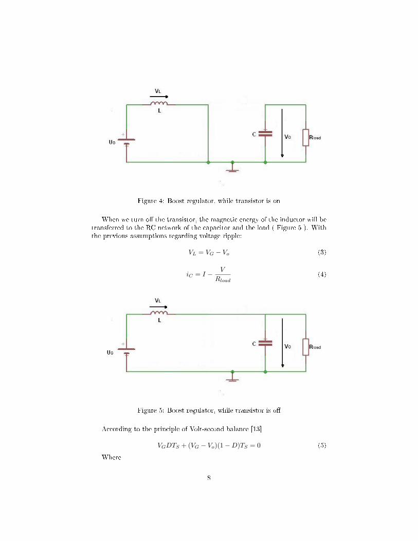
Figure 4: Boost regulator, while transistor is on
When we turn o� the transistor, the magnetic energy of the inductor will betransferred to the RC network of the capacitor and the load ( Figure 5 ). Withthe previous assumptions regarding voltage ripple:
VL = VG − Vo (3)
iC = I − V
Rload(4)
Figure 5: Boost regulator, while transistor is o�
According to the principle of Volt-second balance [13]
VGDTS + (VG − Vo)(1−D)TS = 0 (5)
Where
8

D is the duty cycle D = TON
TS,0 ≤ D ≤ 1,
TON is the duration while T was on,and TS is the switching period.If we solve equation 5 we can calculate the DC gain:
VO
VG=
11−D
(6)
This equation states that the output voltage of a boost converter cannot besmaller than its input voltage.
Equation 6 is only true, if the current in the inductor never falls to zeroduring the entire switching cycle. If this condition is met the circuit is said to bein continuous mode of operation. Otherwise, the circuit will enter discontinuousmode and the equations describing its behaviour will be more complex. Theirderivation can be found in [13] and [12].
3.2 Output stage
In the muscle stimulator device a boost converter will be used to generate theneeded voltage levels for a prescribed current amplitude. It is a simple ande�ective solution, and it was used in commercial stimulators available o� theshelf.
Let's substitute Rload in Figure 3 by the skin and tissue resistance of thepatient under therapy. This setup would supply constant current through theskin, and considering the high skin and tissue impedance discussedin section 2.4,almost unity duty cycle would be needed for current levels in the magnitude ofmilliamps. Practically this is unattainable, as the non zero inductor resistancedrastically decreases the d.c. gain if D ≈ 1[12].
Instead of this, Rload will be substituted according to Figure 6.
Figure 6: Stimulator output stage
9

With the newly introduced components it is possible to deliver current pulsesfor the patient, who is symbolised in the schematic by Rskin.
Switching on transistor T2 opens transistor T4 and T6. If we keep transistorT3 closed, current from the boost converter will �ow through T4, Rskin, and T6to ground. Opening T3, on the other hand, determines a current path throughT5 and T7 ( provided T2 is closed ), which delivers current to the patient withopposite polarity. This setup enables the stimulator to transfer monophasic orbiphasic current pulses, according to how transistors T2 and T3 are driven. Itis very important not to open T2 and T3 at the same time, as this would causea short circuit at the output of the boost regulator, which could ultimatelydestroy the device. Microcontroller software guarantees that this condition cannever happen.
From the boost converter's point of view it is indi�erent what the path ofcurrent is, as long as it �ows through Rskin. This, however, will not be the caseduring most of the time. If both T2 and T3 are closed ( no pulses are currentlydelivered ), Rload will be high impedance, through which the capacitor of theSMPS cannot discharge at all. This prevents steady state operation, the outputvoltage will rise after each switching cycle and the equations of continuous mode(Equation 6) or discontinuous mode in [13] and [12] will fail. No other literaturewas found to discuss the above described condition, the following analysis ismy own work, although the inital equations were based on the description ofdicontinuous mode of operation in [13].
The following discussion presumes that the switching frequency (fs) of theSMPS is much higher than the frequency of pulse repetition(fpulse), and the timeinterval between pulses(tpulse) is much longer than the pulse duration (Tp):
fs =1Ts
>> fpulse (7)
tpulse =1
fpulse>> Tp (8)
First, let's observe the behaviour of the boost regulator in Figure 3 with noload (Rload =∞). This condition can be described by a transient discontinuousmode of operation ( the inductor current falls to zero in each switching period).
When the transistor T1 is turned on, ( Figure 4, Rload =∞)
VL = VG (9)
iC = 0 (10)
The di�erential equation describing the relationship between inductor cur-rent and voltage states:
VL = LdILdt
(11)
10

Integration over time and equation 9 shows, that while T1 is on, current inthe inductor increases linearly [13]:
IL = Io +1L
ˆVLdt =
VGt
L(12)
where Io is the current �owing in the inductor at the beginning of the switch-ing cycle.
Because of the transient discontinuous mode of operation Io = 0, the induc-tor transfers all of its energy to the capacitor in each cycle. As soon as ILdropsto 0, D diode becomes reverse biased and stops conducting which avoids anyfurther decline of Io (see Figure 7 ).
The maximal current in the inductor is
IL,max =VGTon
L(13)
where
Ton = DT =D
fs(14)
When T1 is turned o� ( Figure 5, Rload =∞)
VL = VG − Vo (15)
iC = IL (16)
Using equation 11, equation 13, and the fact that after T1 closes the initialinductor current is Io = IL,max
IL = Io +1L
ˆVLdt = IL,max +
(VG − Vo)tL
(17)
This is a linearly decreasing function as Vo > VG.If tI=0 is the time, after which ILdrops to 0,
VGTon
L+
(VG − Vo)tI=0
L= 0 (18)
Solving this equation yields:
tI=0 =VGTon
VG − Vo(19)
The waveforms of ILand VL are shown in Figure 7.
11

Figure 7: Inductor current and voltage in a boost regulator ( no load )
Let's calculate the output voltage of the boost regulator.According to the di�erential equation describing the relationship between
capacitor current and voltage
IC = CdVo
dt(20)
This means that the capacitor's output voltage rise in each cycle can beexpressed as:
4Vo =1C
Tsˆ
0
ICdt (21)
From equation 10 and 16 we know that current only �ows in the capacitorwhile T1 is o�:
4Vo =1C
tI=0ˆ
0
ICdt =1C
tI=0ˆ
0
ILdt =1C
IL,maxtI=0
2(22)
12

Substituting equation 13 for IL,maxand equation 19 for tI=0
4Vo =V 2
GT2on
2LC(VG − Vo)(23)
Let VO1 be the output voltage Vo at the beginning of the switching cycle,and VO2 after it.
Then
4Vo = VO2 − VO1 =V 2
GT2on
2LC(VG − VO2)(24)
Solving this equation for VO2 yields:
VO2 =VG + VO1 +
√(VG + VO1)2 − 4(VO1VG − (V 2
GT 2on
2LC ))
2(25)
This equation expresses that the output voltage of a boost regulator withno load rises consistently in each switching cycle from VO1to VO2.
Assuming the battery voltage VG, the duty cycle and the switching frequency( thus Ton ) are constant during the operation of the boost regulator, then theexcess voltage gained in each cycle depends solely from VO1.
It can be shown that the gained excess voltage 4V becomes smaller, as theoutput voltage VO rises. From equation 23
limVo→∞(4Vo) = limVo→∞(V 2
GT2on
2LC(VG − Vo)) = 0 (26)
The reason for this is that as V o rises it takes less and less time for theinductor current to drop to 0 (tI=0), thus the capacitor will have less and lesstime to charge.
This can also be shown from equation 19:
limVo→∞(tI=0) = limVo→∞(VGTon
VG − Vo) = 0 (27)
The above described behaviour and the resulting equations were also veri�edby Spice simulations ( Figure 8a and 8b).
Now let's consider the behaviour of the stimulator while T2 or T3 is closed,which means that a pulse is currently being delivered.
The boost regulator now 'sees' the skin and tissue resistance as load, andprovided the boost converter is stable, the output voltage will move towardsits steady state level in discontinuous mode ( Rskin is too high for the boostregulator to operate in continuous mode ). As discussed earlier in this chapter,this steady state output voltage is much smaller, so it is a fair approximationthat this process can be described by the exponential discharge of the capacitorthrough Rskin ( small ripple approximation can evidently not be used here ).
The decline of VO during the pulse can be estimated by
13

(a) Spice simulation: Boost regulator's capacitor voltage, VG = 3V, L=500 µH, C=0.1µF , fs = 10 kHz, D=20%. It can be observed that voltage only rises while transistor T1is o� and diode D is on, which results in a step-like waveform
(b) Spice simulation: Boost regulator's capacitor voltage, VG = 3V, L=500 µH, C=0.1µF , fs = 10 kHz, D=20%. It can be observed that voltage doesn't rise linearly due tothe diminishing tI=0.
Figure 8: Spice simulations of rising output voltage, if boost converter's load isremoved
14

4Vo = −VO1e− Tp
RC (28)
WhereTp is the pulse durationand UO1 is the capacitor's output voltage before the pulse.The stimulator's output stage in Figure 6 will �nd its steady state of oper-
ation, if the net change in capacitor voltage between pulses is zero ( capacitorcharge balance [13] ), thus the gained voltage between pulses equals the lostvoltage during a pulse, expressed in equation 28.
If N switching cycles occur between two stimulation pulses, N can be ex-presses as
N =Tpulse − Tp
Ts(29)
As a reminder:TP is pulse duration,Tpulse is the time interval between two pulses,Ts is the switching period of the boost converter.The total inter-pulse voltage gained can be calculated recursively using equa-
tion 25:
VO2 =VG + VO1 +
√(VG + VO1)2 − 4(VO1VG − (V 2
GT 2on
2LC ))
2
VO3 =VG + VO2 +
√(VG + VO2)2 − 4(VO2VG − (V 2
GT 2on
2LC ))
2
...
VON =VG + VO(N−1) +
√(VG + VO(N−1))2 − 4(VO(N−1)VG − (V 2
GT 2on
2LC ))
2Using equation 28, steady state is achieved if
VON − VO1 = VONeTpRC
The above described method is an accurate way to determine output volt-age of Figure 6 , but it would be very demanding task for a microcontroller. Itrequires lots of processing power and memory because of the recursive calcu-lations. Therefore, it was not implemented, but it can be used for simulationpurposes. Figure 9a shows my Spice simulation, as the circuit in Figure 6reaches its steady state, and Figure 9b shows the typical waveform of a singlepulse in steady state. The decline of the pulse top is an inevitable result of thecapacitor's discharge process.
15

(a) Transient response of output stage, VG = 3V, L=500 µH, C=0.1 µF , Rskin = 5kOhm, fs = 10 kHz,D=20%, Tp = 50µs, Ts = 15ms, biphasic pulses, Blue - current delivered through patient, Green - outputvoltage
(b) Closeup on a single pulse, VG = 3V, L=500 µH, C=0.1 µF , Rskin = 5kOhm, fs = 10 kHz, D=20%,Tp = 50µs, Ts = 15 ms. Blue - current delivered through patient, Green - output voltage
Figure 9: Spice simulation of output stage
16

3.3 Selection of circuit components
The discussion above assumed that all circuit elements are ideal, which is notthe case in practice. Keeping the price of the �nal device down requires somesacri�ces when it comes to selecting the right parts. The following discussionexamines what key component characteristics needed extra attention during thisdesign step [13].
� Switching frequency
High switching frequencies must be generally avoided, as switching losses drasti-cally reduce the e�ciency of the power conversion. On the other hand increasedswitching frequencies also enable the converter to reach higher output voltageswith lower duty cycles, reducing the maximal current �owing in the inductors.The time to reach steady state operation also becomes faster. Empirically 5.7kHz was found to be optimal.
� Transistor
In a regular boost converter operating in continuous mode usually a MOSFETis suggested as it has superior switching times compared to bipolar junctiontransistors (BJT). In that case, increasing the switching frequency can reducethe voltage ripple even with smaller inductors and capacitors. For the stimulatoroutput stage these issues were less relevant, therefore a BJT was used, whichexhibits lower forward voltage drop and higher breakdown voltage at lower price.This stimulator's output voltage was designed not to exceed 300 V and thetransistor's breakdown voltage was chosen accordingly.
� Inductor
It is crucial for the inductor to have a higher peak current rating than iL,max,which can be calculated from equation 13. With improper design the inductormight overheat or saturate, if duty cycles are pushed too high. Lower induc-tances cause output voltage to rise more rapidly (see equation 25 ), because theyalso increase the total transferred charge in each cycle, and thus also iL,max.For my design L=2.2mH was chosen with a peak current rating of 0.25 A. Theseries resistance of the inductor also introduces losses, although these are onlydominant at high duty cycles. Therefore, in this design series resistance of theinductor is not a crucial point to consider.
� Diode
For high switching frequencies the recti�er's reverse recovery time must be small,as exhibited by Schottky diodes and Fast recovery recti�ers. Forward voltagedrop must also be kept low in order to achieve high e�ciency power conversion.Attention must be paid, that the reverse breakdown voltage is higher than themaximum output voltage, and iL,max ( which is also the maximal diode current) doesn't exceed the peak current rating.
� Capacitor
17

Lower capacitances cause output voltage to rise steeper (see equation 25 ),but they also cause a more rapid decline of pulse tops. Apart from this, highequivalent series resistance introduces losses and thus reduces e�ciency. Lastly,the maximum voltage rating must be higher than 300 V ( or the appropriatemaximal output voltage ).
The selected components can be found in the Appendix under the sectionBill of materials.
3.4 Current consumption
The current consumption of the stimulator in Figure 6 can be determined bycalculating the average inductor current in one switching cycle.
< I >=< IL >=1Ts
Tsˆ
0
ILdt (30)
Using Figure 7 we can calculate the area of the triangles instead of integra-tion:
< IL >=1
2Ts(IL,maxTon + IL,maxtI=0) (31)
With equation 13 to determine IL,max and equation 19 to determine tI=0
< IL >=1
2Ts
VGTon
L(Ton + tI=0) =
12Ts
VGTon
L(Ton +
VGTon
VG − Vo) (32)
Because Vo changes in each cycle the current consumption of the circuit willchange as well ( see Figure 9a ). It will peak before the pulse is delivered, andthe lowest amount of current will be required when the circuit is switched on.
3.5 Closed loop control
As mentioned at the end of chapter 3.2, no simple explicit equation was foundfor the output voltage of the stimulator device. Even if this wouldn't be anissue, the skin and tissue resistance of the patient under therapy varies in broadrange. For these reasons, the presented device would not yet be capable todeliver current pulses with given amplitudes.
As a solution, closed loop control (Figure 10) will be introduced to regulatethe output voltage of the boost converter.
Current through the skin will be measured across a resistor and fed backto the analog-digital converter (ADC) of the microcontroller (MCU). The MCUwill calculate the error signal, apply the controller transfer function and generatea PWM signal to drive the switching transistor of the boost regulator ( as itwas discussed in section 3.2, the output voltage increases as the duty cycle ofthe PWM is increased ). Since current will only �ow through the resistor duringpulses, the sampling and updating of the PWM can only take place at the rate
18

Figure 10: Block diagram explaining the closed loop control of the boost con-verter
Figure 11: The complete output stage of the stimulator
of the pulse repetition frequency, fpulse. This is not an issue, the time constantof the controlled system is relatively high, it might take several pulses untilsteady state is reached ( Figure 9a ).
The �nal schematic of the stimulator's output stage can be seen in Figure11.
As current pulses �ow through Rsense to ground, a proportional voltage willappear on the input of the ADC. Csense damps the rising overshoot from Usense
( the feedback for the ADC ) and Dprotection protects the microcontroller fromhigh voltage spikes. Sampling will take place in the middle of the pulse fromthe average of the exponentially declining pulse top. This approach can driveclose to ideal amount of charge through the tissue.
The upper level of ADC conversion ( full scale ) is 2.5 V, and the maximalcurrent amplitude is 125 mA, thereforeRsense = 20 Ohm was chosen.
The controller will be a digital integral controller. Its software implementa-tion will be explained in section 5.1.
19

4 Wireless communication
One of the most distinctive features of the surface stimulator in this project wasthat it must be controlled over a wireless communication channel from a PC.There were several ICs as candidates for this task, but �nally Chipcon AS's (subsidiary of Texas Instruments ) CC1000 transceiver chip was selected.
4.1 CC1000
The following discussion will describe the relevant features of the chosen wirelesstransceiver based on [21], [22], and [25]. The layout of the wireless chip and itsexternal components was made based on [23] ( it can be found in the Appendix).
The CC1000 features extremely low power consumption compared to its al-ternatives due to Chipcons's 350 nm CMOS SmartRF® technology. Combinedwith the ultra low power MSP430 microcontroller ( to be discussed later ) it canprovide extended battery lifetime which was crucial in my application. Further-more, contrary to TI's newest sub 1 GHz CC1101 chip, the CC1000 is availablein a 28 pin Thin-Shrink Small Outline Package (TSSOP) which can be solderedmanually.
The CC1000 can transmit data in the ultra high frequency (UHF) radio bandfrom 300 MHz to 1 GHz. In Europe the 433 MHz and the 868 MHz ISM ( In-dustrial, Scienti�c and Medical ) bands are available for customer speci�c radiotransmission without a licence[14], from which the 433 MHz band was selected,as it allows extended working range and reduced power consumption ( see Ta-ble 2). Its drawback is the longer antenna required for the perfectly matchedcondition, but with the adjusted output power of P=0 dBm, sub-optimal designshould also comply with the speci�ed working range ( the whole system shouldbe kept in a room ). If extended reach will be needed one can easily increasethe output power to 10 dBm, but only at the cost of increased consumed power.Nevertheless this rise shouldn't be signi�cant, as I put overwhelming e�ort intailoring a current consumption pro�le which keeps the IC in power down modeduring most of its operation time.
433 MHz 866 MHz
Receive mode 7.4 mA 9.6 mAPower down mode 200 nA
Transmit mode / P=-20 dBm 5.3 mA 8.6 mATransmit mode / P=-5 dBm 8.9 mA 13.8 mATransmit mode / P=0 dBm 10.4 mA 16.5 mATransmit mode / P=5 dBm 14.8 mA 25.4 mATransmit mode / P=10 dBm 26.7 mA N/A
Table 2: Typical current consumption of the CC1000 [21]
The CC1000 uses frequency shift keying (FSK) to modulate the incoming
20

digital datastream into radio waves.FSK systems vary the frequency of the carrier wave to represent binary ones
and zeroes:
sm(t) = Acos(2πt(fc ± fD)) (33)
Wheresm(t)is the modulated signalA is the amplitude of the modulated signalfcis the carrier wave frequency andfDis the frequency deviationOne of the unpleasant property of the FSK modulation is that the modulated
signals' theoretical bandwidth is in�nitely wide, which means that it cannot betransmitted in a bandlimited channel. Fortunately however most of the spectralcomponents are found in a band near the carrier frequency, as can be seen fromFigure 13[21]. The practical bandwidth of the power spectrum was estimatedusing Carson's rule[15]:
B = 2(fD + Fm) (34)
WherefDis the frequency deviationFmis the modulation frequency.The parameters of the system are stored in a control register block, which can
be read and modi�ed by a 3-wire serial interface, comprising of PDATA, PCLK,and PALE. I used TI's SmartRF Studio software to calculate the contents ofthe con�guration registers for my speci�ed transmission band.
The operation of the CC1000 can be understood from its block diagram inFigure 12:
According to their function we can distinguish three parts of the system[21]:
� The frequency synthetiser and FSK modulator
� The receiver
� and the transmitter
The frequency synthetiser consists of a voltage controlled oscillator (VCO) anda phase locked loop (PLL) circuit which receives its reference signal from astable external crystal oscillator running at 14.7456 MHz. Apart from that, allblocks of the PLL and VCO, including the phase detector, the charge pump,and the frequency dividers (/N, /R) are integrated on the chip, with the onlynotable exception of the external inductor of the VCO. This component wasfound very crucial to be precisely tuned to the center frequency, otherwise thePLL would not be able to lock. This is only achievable with an inductor withL=33 nH, featuring high Q factor and low tolerance. It must also be notedthat the PLL is very sensitive to temperature and supply voltage variations,
21

Figure 12: Block diagram of the CC1000 [21], with permission of TI
for which it must be calibrated at startup. This can be done automatically byissuing the appropriate command to the control registers.
In transmit mode the PLL multiplies the crystal oscillator's low frequencyto generate the modulated radio signal by setting the frequency dividers of thePLL. The con�guration registers have to be previously programmed to containthe parameters of the FSK modulation, such as fc = 434.092 MHz center fre-quency and fD = 32 kHz frequency deviation, which is the maximum adjustablevalue. Keeping the frequency separation high increases the sensitivity of the re-ceiver, but also broadens the bandwidth. With a bitrate of 9.6 kbit/s we canuse Formula 34 to calculate the practical bandwidth of the system, which is 83.2kHz. The resulting transmitted power spectrum can be seen in Figure 13. Wecan see that the whole occupied frequency region is within the ISM band.
The modulated signal is fed to the power ampli�er of the transmitter whoseampli�cation was set to 0 dBm by software.
As receiver the CC1000 follows the superheterodyn principle, thus after alow noise ampli�er the modulated radio signal is converted down to an inter-mediate frequency (IF) of 150 kHz. The local oscillator signal of the mixer isgenerated by the frequency synthetiser. The IF signal is then ampli�ed andthe unwanted frequency components are removed by an internal IF �lter afterwhich the demodulator recovers the digital data stream on the DIO line. Datadecision and synchronisation are also provided on chip, the falling edge clocksignal on DCLK will indicate valid data on DIO. This can ease the workloadof the microcontroller considerably since it can trigger external interrupts onsignal transitions of DCLK.
In order to synchronise data precisely the CC1000 encodes the incoming Non-
22

Figure 13: Transmitted power spectrum of the FSK modulated system, roughestimation
23

Figure 14: Synchronous Manchester encoding [21], with permission of TI
Return-To-Zero (NRZ) datastream into Manchester code before modulation,which ensures that there will be at least one signal transition during each bitperiod and keeps the datastream DC balanced[21].
Keeping the signal DC balanced helps to �nd the correct threshold valuefor the data slicer in the demodulator. This threshold value is presented byan averaging �lter which was set to be free running in the properly DC bal-anced Manchester encoded datastream. Nevertheless every data packet shouldstart with at least four bytes of alternating 1s and 0s, otherwise the sensitivityfor a given bit error rate (BER) would be greatly reduced. The application'sdata rate, center frequency, frequency separation and preamble length togetherpredict the sensitivity of the receiver, which is -104.7 dBm for BER=10−3.
The CC1000 has half duplex communication capability, but in this projectonly simplex communication was required by the unidirectional data �ow fromthe PC to the stimulator. This could keep the embedded software simpler, andit allowed for a more e�cient power management ( see section 5.1.2). The datarate was set to be 9600 bit/s, but it could be amended to 38.4 kbit/s or even76.8 kbit/s if we turned o� Manchester encoding (which uses twice as muchbandwidth as NRZ). In this application this was also unnecessary as very smallamount of data is to be transmitted, but both of these features might be usefulif data acquisition functionality was to be added in the future ( see section 8 ).
4.2 Antenna design
The employed antenna is a meandering monopole radiator integrated onto thePCB, similarly to a transversal helix antenna. [16] suggests that such designshould go as long as possible perpendicular to the ground plane, otherwiseparasitic capacitance to ground and inductance due to bends will be introduced,
24

which reduce the e�ciency. Unfortunately considering this guideline would havemeant an intolerable increase in circuit board area, thus, again the optimumworking range was to be traded for reduced size.
The ideal length of a monopole antenna in free space must be one quarterof the electrical wavelength, which is
L ≈λ
4=
c04 ∗ f
=3 ∗ 108
4 ∗ 434 ∗ 106≈ 17.3cm (35)
WhereL is the length of the antennaλ is the electrical lengthc0 is the speed of light in free spaceand f is the frequency of the signalThe actual length of the antenna on the design was shorter ( approximately
13 cm ), which can be justi�ed by the fact that PCB has a dielectric constantεr > 1, subsequently light propagates slower which results in a shorter idealantenna length ( see equation 35 ). Nevertheless the optimal length could onlybe determined by measuring the antenna impedance with a vector network anal-yser, and �ne tuning the radiator length, the matching inductor and matchingcapacitor values until e�ciency is maximalised[16].
25

5 Overall system description
The complete wireless stimulation system consists of the following blocks:
� Personal Computer / Laptop
The therapist can remotely con�gure the stimulator from a PC equipped withan RS232 serial port, which issues the desired commands through the serialcable to the RS232/wireless interface board.
� RS232/Wireless Interface board
It receives the commands from the PC through its serial interface, organizes theincoming bytes into packets and transmits them to the stimulator wirelessly.
� Wireless stimulator
It performs neuromuscular stimulation and receives the stimulation parametersover a radio frequency link from the RS232/Wireless Interface board.
Figure 15: The wireless stimulation system
Two circuit boards needed to be designed for this project, that of the wirelessstimulator and that of the RS232/wireless interface. In the following sections,they will be discussed independently.
5.1 Wireless stimulator
5.1.1 Hardware description
The block diagram of the wireless stimulator is shown in Figure 16. The micro-controller handles con�guration and data exchange with the CC1000 chip over aserial interface. It controls the stimulator output stage with its PWM channelsand processes the feedback. It alerts the user with an LED, if stimulation is inprogress.
Microcontroller selection
The MSP430F2122 is a relatively cheap, yet powerful mixed signal microcon-troller (MCU) from Texas Instruments with extremely low power consumption,which makes it suitable in portable, battery powered applications[18, 17, 19].It features a 16 bit RISC architecture, which together with its adjustable, max-imum 16 MHz internal crystal oscillator facilitates fast instruction execution
26

Figure 16: Block diagram of wireless stimulator
times. Several peripherals are integrated on chip ( Figure 17), including two16 bit Timers, suitable for generating two independent PWM channels for thestimulator's output stage, an Universal Serial Communication Interface (USCI)which can be con�gured to receive serial data in UART format from the RS232port of the PC, and a fast 10 bit successive approximation analog-to-digital con-verter (ADC), which can directly digitalise the feedback of the digital controller.
Figure 17: Functional block diagram of the MSP430F2122 microcontroller[17],with permission of TI
The IC's power consumption is2.4 mA at 8 MHz, but it can be reduced to560 µA by turning the MCU to low power mode LPM0. Thanks to a versatileclock system waking up from low power mode to active mode is extremely fastand easy compared to other microcontroller families[19].
This MCU has up to 24 GPIO pins of which only six are needed, �ve forinterfacing with the CC1000 chip and one for the LED. Some other pins wereassigned to active peripherals, such as the Timer, and the ADC.
The MSP430F2122 has 512 Bytes of integrated SRAM and 4 kB of Flashmemory. The latter can be upgraded to 8 kB by replacing the chip to theMSP430F2132 variant, whose internal features match the MSP430F2122 except
27

for the extended Flash.The MCU is available in a small, 28 pin Thin-Shrink Small Outline Package
(TSSOP), which could be soldered manually at the university.
Development tool
The MSP430F2122 was programmed and debugged with the MSPFET430UIFFlash Emulation Tool (FET) via 2-wire JTAG (Spy-Bi-Wire) communication.I built a programming interface board ( its schematic can be found in the Ap-pendix ) which included a standard 14 pin JTAG connector and all externalcomponents and signal connections which are only necessary for successful pro-gramming, but not for the correct operation of the device, after the programmerwas detached. The stimulator and the RS232/Wireless interfacing board can beprogrammed after the MSPFET430UIF pod is connected to the JTAG connec-tor andthe necessary connections are made with the programmed board. Thetarget board's power is supplied from the pod, therefore any on-board batterymust be deactivated.
Wireless communication
The CC1000 wireless transceiver chip has a 3-wire serial con�guration interfaceand a 2-wire serial data interface. Five GPIO pins of the microcontroller arededicated for handling communication with these interfaces using a techniquecalled 'bit banging'. At the data rate of 9.6 kbit/s the extra workload is neg-ligible for a powerful microcontroller, like the MSP430[22]. A more detaileddiscussion about the CC1000 chip can be found in Section 4.1.
Power supply
The MSP430F2122 MCU's supply voltage spans from 1.8V-3.6V, while that ofthe CC1000 wireless transceiver ranges from 2.1-3.6V. With this in mind, a 3V2032 Lithium Battery was chosen as power supply, which is situated on the backside of the PCB. From such a battery the MCU can only run reliably with CPUfrequencies at 8 MHz. ( It must be mentioned, that there is no voltage regulatoron the design, which means that the supply voltage will decline with the agingof the battery. According to [17] both the MCU at 8 MHz and the CC1000chip can work reliably with supply voltages over 2.2 V, which was considereda fair safety margin. ) With the MSP430F2122's powerful RISC architecture Ifound 8 MHz of master clock frequency acceptable for this application, and thereduction of processing speed also reduced the current consumption of the IC.
5.1.2 Software description
One of the highlights of the MSP430 microcontroller is the ease, by which it canswitch between active mode and low power mode[19]. In order to utilise thisfeature I assigned most of the tasks to peripherals, which trigger interrupts to
28

wake up the microcontroller from low power standby mode if needed. The maintasks that had to be handled by software were the following:
� The PWM channels of the stimulator output stage could be generated en-tirely by the two Timers, the CPU only has to intervene if the stimulationparameters need to be updated. The digital controller's algorithm couldbe also triggered by one of these Timers.
� The communication with the CC1000 chip could be triggered by the exter-nal interrupts of the wireless transceiver bene�tting from the data synchro-nisation mechanism it employs. In order to reduce the power consumptionof the CC1000 chip it is kept in power down mode most of the time, andit is woken up regularly to check for valid tra�c. This technique is calledpolling[22]. As all regular timers were busy generating PWM for the out-put stage, I had to recon�gure the Watchdog Timer (WDT) to schedulethe polling. The WDT was also used for timing the blinking of the LEDafter system startup.
As we can see, after the system initialisation the code architecture is completelyinterrupt driven according to the recommendation of TI [24]. However, theinterrupt service routines (ISR), especially that of the CC1000 communicationhandling are fairly long, and no interrupt nesting is supported. As a result,some interrupts may never be served. TI recommends to handle all interruptsin the main loop, the ISR should set a �ag according to what action needs tobe taken and only execute code which is urgent[24].
The �owchart of the main() function in Figure 18 demonstrates this concept.
29

Figure 18: Main() function of wireless stimulation software
The boost converter and Timer_A1
The PWM for the switching transistor of the boost converter was generated withone of the MSP430 microcontroller's general purpose 16 bit timers, Timer_A1.
It's Timer/Counter register (TAR) was con�gured to increment from 0 upto the value in the �rst channel of capture/compare registers (TACCR0), thenjump back to zero ( see Figure 19a. ). The counting was triggered by the risingedge of the 8 MHz digitally controllable oscillator (DCO). If the content of TARequals TACCR1 ( the second channel of capture/compare registers ), a compareevent occurs, which updates the PWM output without the need for softwareintervention. This provides very precise timing.
As it can be seen in Figure 19a, the frequency of the output signal is deter-mined by TACCR0, and the duty cycle by TACCR1.
It was already mentioned, that the boost converter's optimal switching fre-
30

(a) The output of Timer_A1 in Up mode (b) The outputs of Timer_A0 inUp/Down mode
Figure 19: PWM generation of Timer_A1 and Timer_A2
quency (fSW ) was found to be 5,7 kHz. This is a relatively low value in orderto reduce switching losses and increase the resolution of the duty cycle that canbe set.
The contents of TACCRx can be calculated as follows:
TACCR0 = fSMCLK
fsw− 1 = 8MHz
5,7kHz − 1 ≈ 1400
and the duty cycle can be calculated as:
D = TACCR1+1TACCR0+1
Pulse width of stimulation current and Timer_A0
Timer_A0 provides the timing of the negative and positive stimulation pulses.It has three Capture compare registers, but channel 0 (TACCR0) is lost for set-ting the upper limit for counting, which determines the frequency. The two re-maining channels can set the duty cycle for each PWM output. Like Timer_A1,Timer_A0 is clocked from the internal 8 MHz DCO, but this time the masterclock is divided by 8 (fSMCLK), since the frequency of stimulation pulses islower that the frequency of switching in the boost regulator.
The timer is operated in Up/Down mode, where the counter counts from 0up to TACCR0 ( capture/compare register for channel 0 ), then back to zero.Centered pulse width modulation ( Figure 19b ) allows the ADC to sampleat the center of the pulse, from the mean of the decaying pulse top, avoid-ing transients. Another advantage of the Up/Down mode is that as long asTACCR1>TACCR2, both outputs cannot switch on at the same time, whichprotects the stimulator in Figure 11 from a short circuit caused by opening T4,T5, T6 and T7 at once.
The duty cycle can be calculated as
D1 = 2TACCR02TACCR1 , and D2 = 2TACCR0
2TACCR12 ,
31

and the frequency of pulse repetition is
Fp = fSMCLK
2TACCR0 .
The frequency of the sub-master clock is 1 MHz, and TACCR0 is a 16bit register, which limits the lowest achievable pulse repetition frequency to 8Hz. This sets no major limitation to the device, because functional electricalstimulation is rarely performed at frequencies below 12 Hz[5]. It is possible todecrease this limit by sourcing the timer from the very low frequency oscillator(VLO), but it is not recommended because measurements suggested that thestimulator output stage behaves unreliably below the frequency of 25 Hz ( seeSection 6).
Again, the output of the PWM is directly connected to the Timer for precisetiming, which produces the periodic output without software intervention assoon as a compare event happens (TAR=TACCR1 or TAR=TACCR2) .
Closed loop control and the Analog-Digital Converter
I implemented a digital Integral controller to regulate the stimulation current.The feedback ( Figure 10 and 11 ) is sampled in the interrupt service routine ofTimer_A0, which is called on the compare event TAR=TACCR0 ( see Figure19b). The rest of the routine is executed in the main loop.
The current is measured across a 20 Ohm resistor. The feedback voltage canbe calculated by
Vin = 20Istim (36)
The analog-digital converter ( ADC ) is a 10 bit analog successive approximationADC.
It has the transfer function
N = 210 Vin − VR−
VR+ − VR−(37)
where VR+ is the upper(2.5V) and VR− is the lower limit (Vss) for conversion[18].Substituting Equation 36 into Equation 37 yields:
N = 210 20Istim − 0(2.5− 0)
=1024 ∗ 20
2.5Istim = 8192Istim (38)
Using this Formula a desired current amplitude can be translated to a desiredADC result (the unit of Istimmust be Amps ).
Besides the digital controller implementation for constant current stimula-tion, current measurement also helps eliminating important safety hazards. Itcan spot a short or open circuit between the electrodes, by comparing N withthreshold values ( too low or too high current ). In either case it immediatelystops the stimulation.
The �owchart of the algorithm can be seen in Figure 20.
32

Figure 20: Algorithm for implementing the digital controller
33

Field Length in bits Usage
Preamble 800 Alternating 0s and 1sStart of Frame Identi�er 8 synchronisation word, it must be 0x33
Packet type 8 'S' for Start, 'E' for Stop, 'U' for Update packetsData 48 Only implemented for 'Update' packets
Table 3: Packet format
Byte Index
1. current amplitude2 MSB of pulse width ( positive pulse )3 LSB of pulse width (positive pulse )4 MSB of pulse width ( negative pulse )5 LSB of pulse width ( negative pulse )6 pulse frequency
Table 4: Data Field of 'Update' packets
Wireless communication
In order to reduce power consumption, the CC1000 chip is kept in power downmode, and awakened at regular intervals looking for data. The Watchdog Timer(WDT) measures the time until the CC1000 has to be woken up. The pollingperiod was set to 50 ms. Such time intervals are too low for the 8 MHz DCO,so the internal 12 kHz 'Very low power, low frequency oscillator' (VLO) had tobe used as clock source instead.
This algorithm requires a supporting communication protocol [25], which isgiven in Table 3.
Each packet must start with a 100 bytes long preamble containing alternat-ing ones and zeros. When used with Manchester encoding ( see section 4.1 ),Chipcon recommends a minimal preamble length of 98 bits ( for best sensitivity) [21]. In order to comply with this, it must be ensured that at least 98 preamblebits are received after the CC1000 chip wakes up, subsequently the length ofthe preamble ( in time ) has to be 98 bits longer than the polling period ( 50ms ). At the data rate of 9600 bit /s, this means the preamble must containat least 578 bits. The large safety margin was left due to the inaccuracy andthermal instability of the VCO ( its actual frequency may vary between 4 and 20kHz)[19]. The end of the preamble is indicated by the Start of Frame identi�er.
All data packets contain a command which depends from the 'Packet type'Field - the 'Start' message initiates neuromuscular stimulation for the patient,the 'Stop' packet turns it o� and the 'Update' message updates all stimulationparameters with the contents of the Data �eld ( Table 4 ).
The software responsible for handling communication with the CC1000 waswritten as a state machine with two possible states. In IDLE state it monitorsthe incoming datastream looking for valid data packets ( Preamble followed by
34

start of Frame identi�er ). If a valid packet header is detected, the programenters RX state, otherwise after a couple of failed attempts the CC1000 is putto standby mode. In RX state the microcontroller extracts data from the pack-ets, analyses them and acts accordingly ( turn on/o� stimulation, or updatesparameters ).
The CC1000 chip provides data synchronisation. An external interrupt cantrigger on the rising edge of DCLK, and apart from reading the valid datafrom the DIO line all further handling is done in the main loop ( see the wholealgorithm in Figure 21).
Figure 21: Flowchart of the wireless communication handling
Development environment
The code for the microcontroller was written in C programming language, andthe development environment was the MSPGCC Toolchain, an open sourceproject to port the GCC (GNU Compiler Collection) toolchain for the MSP430family. It includes the GNU C compiler and its libraries, the assembler, thelinker (binutils), and the debugger (GDB)[20].
Source �les
Table 5 lists and describes the source code �les of the software
35

File name Description
main_rx.c Contains the main programcc1000msp.c Function library for the CC1000 based on [22]cc1000.h Header �le for cc1000msp.cdelay.c Contains functions to delay program executiondelay.h Header �le for delay.c
Table 5: Source �les of the software
5.2 RS232/Wireless interface
5.2.1 Hardware description
Figure 22 shows the block diagram of the RS232/Wireless interface board. TheMSP430 microcontroller ( described in Section 5.1.1 ) communicates with theRS232 port of the PC. It creates packets from the incoming data and transmitsthem to the stimulator board over the wireless link. Due to incompatibility ofthe voltage representation of logical values between the RS232 standard and theMSP430, a MAX3232 chip had to convert the incoming signal to the 3 V stan-dard CMOS voltage level. The incoming serial data is handled by the UniversalSerial Communication Interface (USCI) of the MSP430 in UART mode. Themicrocontroller must also monitor the state of the button and, in case it waspressed, act accordingly (send commands to the stimulator, operate LED).
Figure 22: Block diagram of RS232/Wireless interfacing board
About the microcontroller, the wireless transceiver and the development toolplease refer to Section 5.1.1.
Power supply and current consumption
The size of the interface board was not a critical factor. This allowed me to usetwo bulky AA batteries, which are situated on the back side of the PCB. Thelimitations on CPU frequencies still apply ( see Section 5.1.1), the master clockis sourced from the 8 MHz DCO.
36

5.2.2 Software description
About the development tool and source �les please refer to Section 5.1.2. Themain program is now called main_tx.c
Main() function
The program �ow of the main() function can be seen in Figure 23. I applied thevery same software coding principles, which were emphasized in section 5.1.2.The MSP430 initialises the clock, the I/O ports, the peripherals (Timer_A0for polling the button and the Universal Serial Communication Interface forreceiving incoming serial data), and the CC1000 wireless transceiver, which isimmediately set to power down mode. The endless loop keeps the microcon-troller in low power mode, until an interrupt wakes it up. Again, the interruptservice routines use �ags to communicate with the main loop, where most in-terrupt handling takes place.
Figure 23: Flowchart for Main() function of Interfacing board
37

Wireless communication
The program has two states: in IDLE state there is no data to transmit, themicrocontroller waits in low power mode, until a packet arrives from the PCor the button is pressed. If either of these events occur, the program entersTX state, wakes up the CC1000 and starts sending the individual bits ( seealgorithm in Figure 24 ) on the external interrupts triggered by the falling edgeof DCLK.
Figure 24: Flowchart of external interrupt handling in the main loop
Polling of Button and TIMER_A0
Timer_A0 polls the button regularly in every 40 ms. This is a suitable intervalfor debouncing, and it also allows the microcontroller to stay in standby mode.If the button is pressed, the program creates and sends a 'Start' packet. As soonas the button is released, a 'Stop' packet is transmitted to the stimulator module.The MCU keeps the LED on while the button is pressed, indicating that buttontriggered stimulation is in progress. This feature enables the RS232/wirelessinterface board to be used as remote controller for stimulation. Figure 25 showsthe �owchart of the described algorithm.
38

Figure 25: Timer_A0 ISR for button polling
Universal Serial Communication Interface and communica-tion with the PC
The Universal Serial Communication Interface (USCI) can be con�gured towork similarly like the common Universal Asynchronous Receiver/Transmitter(UART) in embedded systems; it can handle communication with the RS232port of the PC. Data are sent serially in frames, each of which contains one byteof payload, one low level Start bit, and one high level Stop bit ( 8N1 format, noparity bit ). The Baud rate was set to 9600 Bauds. Contrary to the CC1000wireless chip, the USCI can receive and transmit frames of data independentlyby hardware, software only has to read the appropriate registers when the USCIinterrupt triggers. The �owchart of the interrupt handler can be seen in Figure26.
39

Figure 26: The USCI interrupt routine in main loop
40

6 Performance analysis
Current consumption
Almost all design steps focused on the reduction of current consumption ofthe boards. It is crucial to assess, how well this goal was accomplished. Thefollowing section will provide theoretical current pro�les of the two designedPCBs, which will be followed by concrete measurements.
Stimulator board
A failed attempt by the CC1000 to �nd valid preamble lasts approximately 2ms. With the polling period of 50 ms we can conclude, that the chip spendsabout 96% of its lifetime in low power mode. If a valid packet is detected, ittakes maximum 95 ms to receive it ( 912 bits at 9600 bit/s ). Using Table 2and the assumption, that there is very little wireless tra�c, the expected powerconsumption of the CC1000 on the stimulator board can be estimated by:
Iavg,CC1000rec ≈ 0.04 ∗ 7.4mA+ 0.96 ∗ 200nA ≈ 0.3mA
The MSP430 microcontroller spends about 90% of the time in low powermode 'LPM0' , where the CPU and its clock is disabled. The MSP430 is capableto shut down its DCO to conserve even more power, but this feature could notbe used as some peripherals always required the DCO as clock source. Using[17] the current consumption of the microcontroller is:
Iavg,MSP430stim ≈ 0.2 ∗ 2.4 + 0.8 ∗ 0.56 ≈ 0.93mA
The LED (forward voltage drop=0.6V) is operated with a 510 Ohm resistorwith 50% duty cycle, which gives us
Iavg,LED ≈ 12
(3−0.6)510 ≈ 2.3mA
The estimated current consumption of the stimulator output stage is verydi�cult to determine, as it was discussed in section 3.2. An estimation usingequation 32 for fs = 5.7kHz, D=20%, Uo = 200V is: Iavg,boost ≈ 1.6mA.
This results in the total current consumption of the stimulator board, as5.13 mA while stimulation is in progress, and 1.23 mA otherwise. The actualmeasured values were fairly close; 6.4 mA during stimulation and 1.3 mA in'standby'.
The rated capacity of the 2320 battery is 220 mAh, which leaves35 hours ofestimated battery life with and 169 hours without stimulation. The stimulatedlifetime of the device could be extended to 53 hours just by simply removing theLED. Practically these �gures could be misleading, as actual battery capacitystrongly depends on the mean value and distribution of current discharge[26].Figure 7 on the other hand shows that the current drawn from the battery isvery uneven, which might shorten battery life. Nevertheless it can be concludedthat the estimated lifetime of the designed stimulator is highly superior to theRehaStim stimulator, which can only run for 6 hours from a 6 V battery.
41

Interface board
The theoretical power consumption of the interface board was calculated sim-ilarly, as can be seen in Table 7. The CC1000 chip only wakes up if data arewaiting to be sent. This is assumed to be very infrequent, thus power downmode current consumption pro�le was adapted.
current consumption
MSP430 ~1 mACC1000 ~0.2 µA ( in PD mode)MAX3232 1 mA
LED (50% duty cycle) 2.3 mATable 7: Estimated power consumption of the stimulator
This time the measured current consumption was unexpectedly high, 7.6mA while stimulating with the button ( LED �ashes), and 6.3 mA otherwise.Even this gives about 400 hours of lifetime using typical AA batteries.
Stimulation
The stimulator's stimulation capabilities were tested with a load of 1 kOhm.As it was discussed in section 2.4, this is a typical value for well prepared skinsurfaces.
The current amplitude was tested in the range of 5-100 mA. The accuracy ofthe output current was found to be dependent on other stimulationparameters, but generally higher current values could be more precisely set bythe digital controller. This is probably due to the fact that the microcontrollerhas no �oating point unit and it handles fractions with di�culty ( expressed inhigh computational power ), therefore all calculation results were rounded tothe nearest integers. The accumulated error was more explicit while handlinglower numbers ( this phenomenon a�ects the accuracy of all stimulationparameters ). It must also be mentioned, that depending on pulse width themaximal current value of the decaying pulse top was sometimes multiple of thedesired average level. This is due to the fact that the digital controller samplesthe feedback in the middle of the pulse. This approach provides more precisecontrol of the injected charge, than sampling the maximal current value, but itcannot have control over the maximal current �owing through the body. Thisis one of the serious limitations of this design compared to professionalcommercial solutions. The stimulator was found capable of outputting currentlevels in the tested range, while the pulse repetition frequency was 50 Hz andthe pulse width was set to 100 µs (see Figures 27b and 27a).
42

wireless stimulator* RehaStimminimum maximum minimum maximum
Current amplitude 0 100 mA 0 126 mAPulse waveform monophasic or biphasic any
Pulse repetition frequency 25 Hz 300 Hz 1 Hz 140 HzPulse width 40µs 500µs 20µs 500µs
rise time of pulse 1 µs 2 µsnumber of channels 1 8wireless connectivity available not available
Battery life 35 hours from 2 AA batteries 9 hours from 4 AA batteriesSize 5.7 x 4.3 x 2 cm 15.5 x 6.5 x 13.5 cm
Table 8: Characteristics of the wireless stimulator in comparison with the spec-i�ed technical details of RehaStim[2].*The measurement conditions can be found in the text.
The pulse duration was tested with the current amplitude of 20 mA andpulse repetition frequency of 50 Hz. The output stage was found capable ofproducing pulses in the 40-500 µs range, although by measuring PW=500 µsthe output capacitor discharged totally (the voltage dropped to 0) by the end ofthe pulse. This suggests that the entire pulse width spectrum cannot be utilisedunder all conditions ( low current amplitude, etc ). The narrowest pulse widthis also below the capability of RehaStim.
The frequency range of the stimulator was found most de�cient. The boostconverter of the output stage didn't tolerate pulse repetition frequencies lowerthan 10 Hz, and the accuracy of pulse amplitudes were found unacceptable withfrequencies under 25 Hz ( see Figure 27c). The conditions of this measurementwere I=20 mA, PW= 200 µs. The maximal adjustable frequency with accuratecurrent amplitude was 300 Hz ( see Figure 27d).
The rise time of the stimulator was also measured, and it was found to becompetitive with RehaStim ( 200 ns at PW=200 µs, I=20 mA, f=50Hz).
I also carried out measurements with a higher, 5 kOhm load resistor, whichintends to model unprepared skin impedances. With the increased load thepulse tops became �atter ( larger RC time constant ), but the simulatorcouldn't output currents higher than 35 mA ( see Figure 27f). This is thepoint where the inductor in the boost converter saturates and increasing theboost converter's duty cycle results in no further output voltage level gain.Higher current outputs could be achieved by �ne tuning the inductor used inthe stimulator circuit ( see section 3.2 ). For the parameter overview of thedesigned stimulator device, and a comparison with RehaStim, please refer toTable 8.
43

(a) High current monophasic pulses, Rload =1kOhm, I=100 mA, f=50Hz, PW = 100µs
(b) Low current monophasic pulses, Rload =1kOhm, I=5 mA, f=50Hz, PW = 100µs
(c) Low frequency monophasic pulses,Rload = 1kOhm, I=20 mA, f=20Hz, PW =200µs
(d) High frequency monophasic pulses,Rload = 1kOhm, I=20 mA, f=300Hz, PW =200µs
(e) Biphasic pulses, Rload = 5kOhm, I=20mA, of 10 mA, f=50Hz, PWpos = PWneg =100µs
(f) High load high voltage monophasicpulses, Rload = 5kOhm, I=35 mA, f=100Hz, PWpos = 100µs
Figure 27: Oscilloscope measurements of stimulator output pulses
44

Working range
The device could be safely controlled from distances up to 15 m ( although onlylimited tests were made ). Moving away any further might result in packet lossand the unreliable control of stimulation. The working range could be easilyextended by request, if the output power of the CC1000 would be set to 10dBm. It must also be noted that the measurement was carried out indoors,where the device will most likely be operated. Possibly a better performancecould be achieved outdoors due to mitigation of multipath fading[25].
Board size
The dimensions of the stimulator PCB are 5.7 x 4.3 x 2 cm. It should �tcomfortably on the stimulation body surfaces of interest. For multichannelstimulation of various muscle groups at the same time, several stimulator boardscould be used. Section 8 will provide more details about this idea.
Patient safety
The stimulator is absolutely safe and can cause no harm to patients. The worstcase scenario is when the output capacitor is touched while it is charged to 300V, which drives 30 µC (Q=CU) of charge though the human body. This is wellbelow the dangerous limit of 560 µC, as calculated by [27].
45

7 User's guide
While reading the following guide please refer to Figure 28 showing images ofthe designed PCBs.
(a) Stimulator board (b) RS232/Wireless interface board
Figure 28: Front view image of the boards
The following steps are required to set up the stimulator board for neuro-muscular stimulation:
1. Connect the interface board's 9 way D-type connector ( standard RS232connector ) to the RS232 serial port of the laptop or personal computer (alternatively an USB-serial converter can be used )
2. Put the stimulator module's electrodes to the skin surface, where themuscles to be stimulated are located. Note, that the stimulator is still intesting stage, at present a 5 kOhm resistor is placed where the electrodesshould be connected.
3. On the PC/laptop open Matlab and run Stimulator.m. The graphical userinterface (GUI) displayed in Figure 29 will pop up.
4. Set the serial port number in Matlab (it can be checked in Control Panel/System/Hardware/DeviceManager under Windows, or using the 'setserial' command under Linux).
46

Figure 29: Matlab program's graphical user interface
5. Make sure that the red JUMPER RST JP is placed on both the stimulatorboard and the interface board.
6. Turn on the stimulator module and the interface board. Look for a shortblink of the LED indicating that the board is ready for stimulation.
7. Set the required stimulation parameters on the left side of the MATLABGUI. The graph on the right side of the screen will provide a visual rep-resentation of the resulting pulse waveform. Note, that pulse frequency isinterpreted as the frequency of pulses with same polarity, even if biphasicstimulation is selected. The program is protected against entering mean-ingless or invalid input values.
8. Press the Update button to transfer the parameters into the stimulationboard.
9. Press the START button to activate stimulation. It can be stopped anytime with the STOP button. The stimulator parameters can be set run-time as well, the stimulation will continue uninterrupted with the updatedparameters. The 'Stim LED' on the stimulator board always �ashes aslong as stimulation is in progress.
If the stimulation is started before the parameters were programmed, the fol-lowing default values will be assumed:
� Pulse amplitude = 10 mA
� Pulse frequency = 50 Hz
47

� Pulse shape = biphasic
� Positive pulse width = 100µs
� Negative pulse width = 100µs
If a PC with an RS232 port is not available, the stimulator can be directlystarted and stopped with the button on the interface board, like a remote con-troller. Stimulation will occur while the button is pressed down with defaultparameters. The 'Remote Stim LED' on the interface board will start �ashing,to indicate that remote controlled stimulation is in progress.
Developer's guide
Please refer to my notes about the development environment and developmenttools in section 5.1. Connect the FET tool to the USB port of your PC, andto the 14 pin JTAG connector on your programming interface board ( �nd itin the appendix ). Remove RST JP from both boards, and connect the RST,TEST, GND and VCC pins with the corresponding pins on the programminginterface board ( watch out for the right pins on RST JP, shown in Figure 28with labeling). The programming of the board can already be initiated.
48
8 Future development plans
One of the greatest shortcomings of the designed stimulation system is that itis not capable to produce a multichannel output, which is utterly needed inFES. Multiplexing the stimulation output is a possible workaround in futureversions of the design, however the small size of the stimulator board enablesthe application of several boards on the intended muscles. This solution requiresminor modi�cations in software. The communication protocol ( Table 3 ) mustbe extended with a �eld that identi�es the address of the stimulator, and allowsindependent control for all stimulator boards in use. The addresses can be staticwith the modi�cation of the embedded software in each stimulator device, orthey can be dynamically distributed from the PC. The latter solution wouldrequire the implementation of half duplex communication, which could be easilydone based of the currently running code.
The implementation of half duplex communication can o�er further advan-tages in future versions. A more reliable wireless communication could be es-tablished by handshaking, the stimulator could send an acknowledge packet tonotify the PC of the successful reception of a packet. The packet could alsocontain an 8 bit checksum or CRC (cyclic redundancy check ), which could ver-ify the data integrity. If needed, request for retransmission could be sent to thePC.
In the current design, monophasic, or biphasic pulses can be produced withgiven frequency, pulse width and current amplitude. The �exibility of the pulsewaveforms could be greatly enhanced, if the PWM determining the pulse widthswould be generated by the ISR of the Timer in continuous mode. Although thisrequires additional processing and thus increased current consumption, burstsof pulses could be produced with entirely arbitrary waveform ( only currentamplitude would be �xed ). A bu�er could contain the parameters of the pulsesin blocks of 2 bytes, one byte determining the pulse width, and the next bytethe space until the next pulse. One bit of either of these bytes could be reservedto determine the phase of the pulse. The Timer could circularly read this bu�erand repeatedly measure the time until the next pulse transition. This wouldalso mean a reduction in accuracy compared to the hardware driven solution,but it o�ers endless �exibility.
Although not directly related to FES, muscle training often requires 'mod-ulation mode' stimulation where the pulse amplitude is gradually increased[3]for elevating muscle stress. This could be also implemented with the abovedescribed modi�cation, although the digital controller needs certain number ofpulses to set the desired current amplitude, which limits the rate of currentamplitude rise.
Apart from the channel multiplexing, all suggestions so far could be eas-ily implemented by sole software amendments with little e�ort. The followingsuggestions require extension of hardware which results in size and current con-sumption increase. It must be carefully evaluated if it is worth this compromise.
The current design includes no voltage regulator, which might result in theunpredictable operation of the device with sinking battery voltage. A DC-DC
49

converter IC could be adapted for this task. As an alternative solution theMSP430 microcontroller's analog-digital converter is capable of measuring thesupply voltage, and a low battery indicator LED could notify the user if needed.
The capabilities of the CC1000 chip are far beyound the current implemen-tation of the device. It could be further exploited for various research projects.For instance biosignals (EMG, EEG, ENG) could be acquired and transmittedto the PC wirelessly, which could be processed as feedback to closed loop con-trolled neuroprostheses. This is one of the emerging technologies, which mightpromise a breakthrough in the rehabilitation of paraplegics[5].
50

9 Conclusion
A transcutaneous neuromuscular stimulation system has been designed and im-plemented. The stimulator device can generate high voltage constant currentregulated faradic stimulation pulses with �exibly adjustable current amplitude (0-100 mA), pulse width ( 40-500 µs ) and pulse repetition frequency (25- 300 Hz).These parameters can be con�gured remotely from a personal computer over awireless link. The entire system is operational, including the stimulator boardresponsible for generating the high voltage pulses, an interface board which di-rects the commands from the PC to the stimulator over a radio frequency link,and the Matlab software which interacts with the operator through a graphicaluser interface.
Even though the quality of produced waveform is inferior to professionalcommercial solutions, like RehaStim ( decaying pulse top, only one channel, less�exible pulse waveform, etc. ), the wireless connectivity, cheaper cost, smallersize, lighter weight, and prolonged lifetime from battery make the presentedstimulation system a competitive product in numerous applications. Althoughit was specially designed for functional electrical stimulation, its capabilitiesmake it universally deployable in therapy, as well as research.
51

Appendix
Schematic of stimulator board
52

Layout of stimulator
Top:
Bottom:
53

Stimulator Bill of Materials
reference description value
C1 400 V SMD capacitor 0.1 µFC2 electrolytic capacitor 10 µFC3 ceramic capacitor 0.1 µF
C_C1 SMD tantalum capacitor 3.3 µFC_C6 SMD ceramic capacitor 33 nFC_C10 SMD ceramic capacitor 12 pFC_C11 SMD ceramic capacitor 220 pFC_C12 SMD ceramic capacitor 1 nFC_C14 SMD ceramic capacitor 68 pFC171 SMD ceramic capacitor 18 pFC181 SMD ceramic capacitor 18 pFC41 SMD ceramic capacitor 8.2 pFC42 SMD ceramic capacitor 5.6 pFC31 SMD ceramic capacitor 15 pFL inductor, 220 mA 2.2 mHL41 SMD inductor 6.2 nHL101 SMD inductor, high Q 33 nHL32 SMD inductor 68 nHT1 npn transistorT2 npn transistorT3 npn transistorT4 pnp transistorT5 pnp transistorT6 pnp transistorT7 pnp transistor
Csense ceramic capacitor 47 nFQ1 SMD crystal 14.7456 MHzR131 SMD resistor 82 kOhmR1 SMD resistor 33 kOhmR2 SMD resistor 33 kOhmR3 SMD resistor 33 kOhmR4 SMD resistor 33 kOhmR5 SMD resistor 510 OhmR6 SMD resistor 1 kOhmR7 SMD resistor 1 kOhmR8 SMD resistor 510 Ohm
Rsense SMD resistor, 0.1% 20 OhmLED1 LED, redD1 SMD diode, 1AD2 SMD diode, 1AuC MSP430F2122
CC1000 CC1000
54

Wireless/RS232 Interface board schematic
55

Layout of Wireless/RS232 Interface board
Top
Bottom:
56

Wireless/RS323 Interface Board, Bill of Materials
reference description value
C1 electrolytic capacitor 10 µFC2 ceramic capacitor 0.1 µFC3 SMD ceramic capacitor 0.1 µFC4 SMD ceramic capacitor 0.1 µFC5 SMD ceramic capacitor 0.1 µFC6 SMD ceramic capacitor 0.1 µFC9 SMD ceramic capacitor 0.1 µF
C_C1 SMD tantalite capacitor 3.3 µFC_C6 SMD ceramic capacitor 33 nFC_C10 SMD ceramic capacitor 12 pFC_C11 SMD ceramic capacitor 220 pFC_C12 SMD ceramic capacitor 1 nFC_C14 SMD ceramic capacitor 68 pFC171 SMD ceramic capacitor 18 pFC181 SMD ceramic capacitor 18 pFC41 SMD ceramic capacitor 8.2 pFC42 SMD ceramic capacitor 5.6 pFC31 SMD ceramic capacitor 15 pFL41 SMD inductor 6.2 nHL101 SMD inductor, high Q 33 nHL32 SMD inductor 68 nHQ1 SMD crystal 14.7456 MHzR131 SMD resistor 82 kOhmR8 SMD resistor 510 Ohm
LED1 LED, redCONN 9-way D-type connector
MAX3232 MAX3232 CUEuC MSP430F2122
CC1000 CC1000
57

JTAG programming interface board, schematic
58

References
[1] Centre for Rehabilitation Engineering, Glasgow University, http://www.gla.ac.uk/cre/
[2] Hasomed GmbH, http://www.hasomed.de
[3] Sheila Kitchen, �Electrotherapy : Evidence based practice, Eleventh Edi-tion�, Churchill Livingstone, 2002
[4] Jaakko Malmivuo, Robert Plonsey, �Bioelectromagnetism - Principles andApplications of Bioelectric and Biomagnetic Fields�, Oxford UniversityPress, New York, 1995.
[5] P. Hunter Peckham, Jayme S. Knutson, �Functional electrical stimulationfor Neuromuscular applications�, Annual Review of Biomedical Engineer-ing, pp. 327-360, 2005
[6] Jay T. Rubinstein, Charles A. Miller, Hiroyuki Mino, Paul J. Abbas, �Anal-ysis of Monophasic and Biphasic Electrical Stimulation of Nerve�, IEEETransactions on biomedical engineering, vol 48, pp. 1065-1070, 2001
[7] A. van Boxtel, �Skin resistance during square wave electrical pulses of 1 to10 mA�, Med and Biol. Eng & Comput, volt 15, pp. 679-687, 1977,
[8] J. Patrick Reilly, �Applied Bioelectricity: From Electrical Stimulation toElectropathology�, Springer, 1998
[9] Stephen J. Dorgan, Richard B. Reilly and Carl D. Murray, �A model for hu-man skin impedance during surface functional neuromuscular stimulation�,Proceedings - 19th International Conference - IEEE/EMBS, pp. 1770-1773,1997
[10] T Ragheb, L A Geddes, �Electrical properties of metallic electrodes�, Med-ical and Biological Engineering and Computing, pp. 182-186, 1990
[11] Perkins TA, �Impedances of common surface stimulation electrodes�, 9thAnnual Conference of the International FES Society, 2004
[12] H.W. Whittington, B. W.Flynn, D.E. Macpherson, �Switched mode powerSupplies : Design and construction�, Research Studies Press Ltd., 1992
[13] Robert W. Ericsson, Dragan Maksimovic, �Fundamentals of Power Elec-tronics, Second Edition�, Kluwer Academic Publishers, 2004
[14] International Telecommunication Union website, http://www.itu.int/
ITU-R/terrestrial/faq/index.html
[15] Ferrel G. Stremler, "Introduction to Communication Systems, Third Edi-tion�, Addison-Wesley Publishing Company, 1997
59

[16] Matthew Loy, Iboun Sylla, Texas Instruments Inc., �Application ReportSWRA046A, ISM-Band and Short Range Device Antennas�, 2005
[17] Texas Instruments Inc., �MSP430F21x2 Mixed Signal Microcontroller,SLAS578D�, 2009
[18] Texas Instruments Inc., �MSP430x2xx Family User's Guide, SLAU144E�,2008
[19] John Davies, �MSP430 Microcontroller Basics�, Elsevier Ltd., 2008
[20] MSPGCC, The GCC toolchain for the Texas Instruments MSP430 MCUs,http://mspgcc.sourceforge.net
[21] Texas Instruments Inc., �CC1000 Single Chip Very Low Power RFTransceiver, SWRS048A�, 2009
[22] K. H. Torvmark, Texas Instruments Inc., �AN009 CC1000/CC1050 Micro-controller interfacing, SWRA082�
[23] Texas Instruments Inc.,� User Manual, Rev. 1.22, CC1000PP Plug andPlay Module, SWRU060�
[24] Keith Quiring, Texas Instruments Inc., �Application Report SLAA294A,MSP430 Software Coding Techniques�, 2006
[25] K. H. Torvmark, Texas Instruments Inc., �Application Note AN015SWRA076 RF Modem Reference Design�
[26] Massoud Pedram, Qing Wu, �Design considerations for battery-poweredelectronics�, Design Automation Conference, pp.861 - 866 , 1999
[27] Kurt A. Kaczmarek, Kevin M. Kramer, John G. Webster, Robert G. Rad-win, �A 16-Channel 8-Parameter Waveform Electrotactile Stimulation Sys-tem�, IEEE Transactions on Biomedical Engineering, 1991
60