Embed Size (px)
Citation preview

April 2008 Rev 2 1/14
14
LF351
Wide bandwidth single JFET operational amplifiers
Features■ Internally adjustable input offset voltage
■ Low power consumption
■ Wide common-mode (up to VCC+) and
differential voltage range
■ Low input bias and offset current
■ Output short-circuit protection
■ High input impedance JFET input stage
■ Internal frequency compensation
■ Latch up free operation
■ High slew rate 16 V/µs (typical)
DescriptionThese circuits are high speed JFET input single operational amplifiers incorporating well matched, high voltage JFET and bipolar transistors in a monolithic integrated circuit.
The devices feature high slew rates, low input bias and offset currents, and low offset voltage temperature coefficient.
NDIP8
(Plastic package)
DSO-8
(Plastic micro package)
�
�
�
�
�
�
�
1 - Offset null 12 - Inverting input3 - Non-inverting input4 - VCC- 5 - Offset null 26 - Output7 - VCC+ 8 - N.C.
Pin connections(top view)
www.st.com

Schematics LF351
2/14
1 Schematics
Figure 1. Schematic diagram
Figure 2. Input offset voltage null circuit
Output
Non-inverting input
Inverting input
VCC
VCC
100W
1.3k
30k
35k 35k 100W1.3k
8.2k
Offset Null1 Offset Null2
100W
200W

LF351 Absolute maximum ratings and operating conditions
3/14
2 Absolute maximum ratings and operating conditions
Table 1. Absolute maximum ratings
Symbol Parameter Value Unit
VCC Supply voltage(1) ±18 V
Vi Input voltage(2) ±15 V
Vid Differential input voltage(3) ±30 V
Rthja
Thermal resistance junction to ambient(4)
SO-8DIP8
12585
°C/W
Rthjc
Thermal resistance junction to case(4)
SO-8DIP8
4041
°C/W
Output short-circuit duration(5) Infinite
Tstg Storage temperature range -65 to +150 °C
ESD
HBM: human body model(6) 500 V
MM: machine model(7) 200 V
CDM: charged device model(8) 1.5 kV
1. All voltage values, except differential voltage, are with respect to the zero reference level (ground) of the supply voltages where the zero reference level is the midpoint between VCC
+ and VCC-.
2. The magnitude of the input voltage must never exceed the magnitude of the supply voltage or 15 volts, whichever is less.
3. Differential voltages are the non-inverting input terminal with respect to the inverting input terminal.
4. Short-circuits can cause excessive heating and destructive dissipation. Values are typical.
5. The output may be shorted to ground or to either supply. Temperature and/or supply voltages must be limited to ensure that the dissipation rating is not exceeded
6. Human body model: A 100 pF capacitor is charged to the specified voltage, then discharged through a 1.5 kΩ resistor between two pins of the device. This is done for all couples of connected pin combinations while the other pins are floating.
7. Machine model: A 200 pF capacitor is charged to the specified voltage, then discharged directly between two pins of the device with no external series resistor (internal resistor < 5 Ω). This is done for all couples of connected pin combinations while the other pins are floating.
8. Charged device model: all pins and the package are charged together to the specified voltage and then discharged directly to the ground through only one pin. This is done for all pins.
Table 2. Operating conditions
Symbol Parameter LF151 LF251 LF351 Unit
VCC Supply voltage 6 to 32 V
Toper Operating free-air temperature range -55 to +125 -40 to +105 0 to +70 °C
Electrical characteristics LF351
4/14
3 Electrical characteristics
Table 3. Electrical characteristics at VCC = ±15 V, Tamb = +25°C (unless otherwise specified)
Symbol Parameter Min. Typ. Max. Unit
VioInput offset voltage (Rs = 10kΩ)
Tmin ≤ Tamb ≤ Tmax
3 10
13mV
DVio Input offset voltage drift 10 µV/°C
IioInput offset current (1)
Tmin ≤ Tamb ≤ Tmax
5 1004
pAnA
IibInput bias current (1)
Tmin ≤ Tamb ≤ Tmax
20 20020
pAnA
AvdLarge signal voltage gain (RL = 2kΩ, Vo = ±10V)
Tmin ≤ Tamb ≤ Tmax
5025
200V/mV
SVRSupply voltage rejection ratio (RS = 10kΩ)
Tmin ≤ Tamb ≤ Tmax
80
80
86dB
ICCSupply current, no load
Tmin ≤ Tamb ≤ Tmax
1.4 3.4
3.4mA
Vicm Input common mode voltage range±11 +15
-12V
CMRCommon mode rejection ratio (RS = 10kΩ)
Tmin ≤ Tamb ≤ Tmax
7070
86dB
IOSOutput short-circuit current
Tmin ≤ Tamb ≤ Tmax
1010
40 6060
mA
±Vopp
Output voltage swing RL = 2kΩRL = 10kΩ
Tmin ≤ Tamb ≤ Tmax
RL = 2kΩRL = 10kΩ
1012
1012
1213.5
V
SR Slew rate, Vi = 10V, RL = 2kΩ, CL = 100pF, unity gain 12 16 V/µs
tr Rise time, Vi = 20mV, RL = 2kΩ, CL = 100pF, unity gain 0.1 µs
Kov Overshoot, Vi = 20mV, RL = 2kΩ, CL = 100pF, unity gain 10 %
GBP Gain bandwidth product, f = 100kHz, Vin = 10mV, RL = 2kΩ, CL = 100pF 2.5 4 MHz
Ri Input resistance 1012 Ω
THDTotal harmonic distortion
f= 1kHz, Av= 20dB, RL= 2kΩ, CL=100pF, Vo= 2Vpp0.01 %
enEquivalent input noise voltage
RS = 100Ω, f = 1KHz15
∅m Phase margin 45 Degrees
1. The input bias currents are junction leakage currents which approximately double for every 10°C increase in the junction temperature.
nV
Hz------------
LF351 Electrical characteristics
5/14
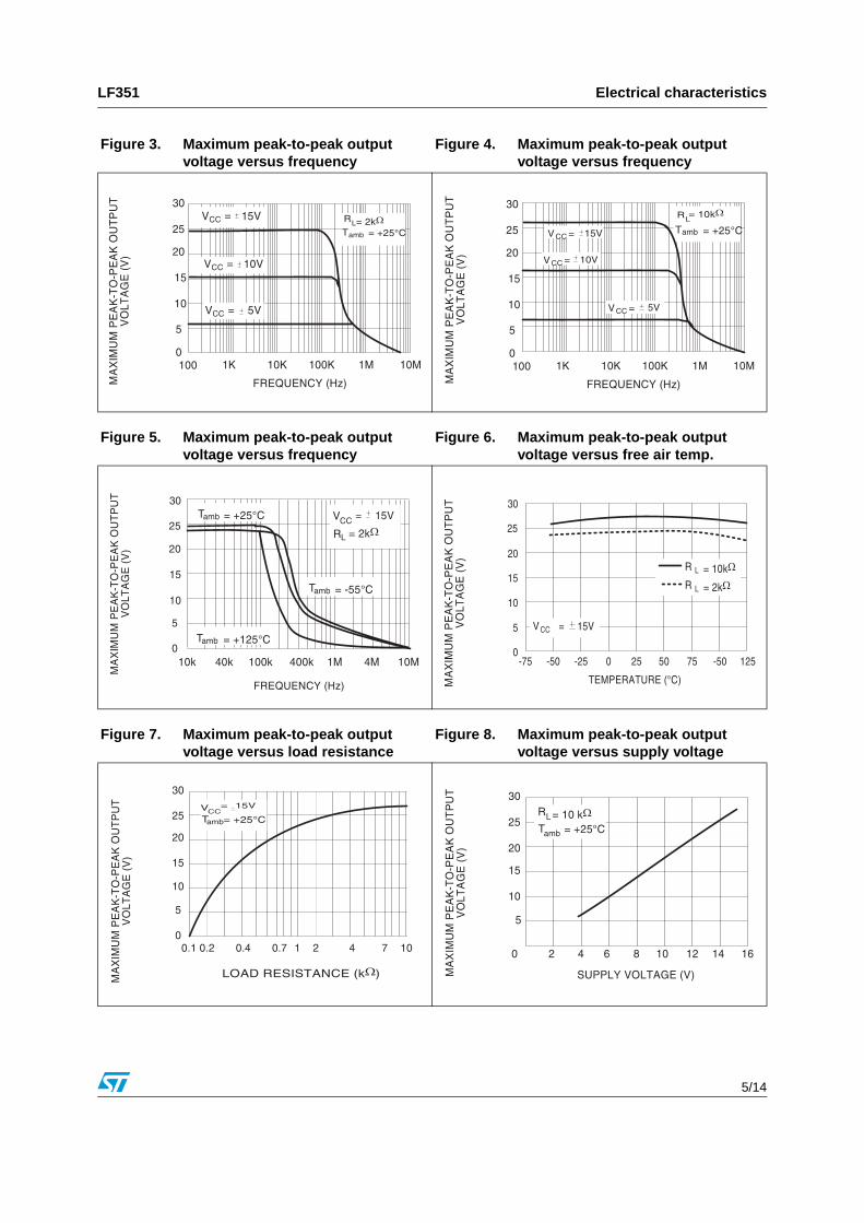
Figure 3. Maximum peak-to-peak output voltage versus frequency
Figure 4. Maximum peak-to-peak output voltage versus frequency
Figure 5. Maximum peak-to-peak output voltage versus frequency
Figure 6. Maximum peak-to-peak output voltage versus free air temp.
Figure 7. Maximum peak-to-peak output voltage versus load resistance
Figure 8. Maximum peak-to-peak output voltage versus supply voltage

Electrical characteristics LF351
6/14
Figure 9. Input bias current versus free air temperature
Figure 10. Large signal differential voltage amplification versus free air temp.
Figure 11. Large signal differential voltage amplification and phase shift versus frequency
Figure 12. Total power dissipation versus free air temperature
Figure 13. Supply current per amplifier versus free air temperature
Figure 14. Supply current per amplifier versus supply voltage

LF351 Electrical characteristics
7/14
Figure 15. Common mode rejection ratio versus free air temperature
Figure 16. Voltage follower large signal pulse response
Figure 17. Output voltage versus elapsed time Figure 18. Equivalent input noise voltage versus frequency
Figure 19. Total harmonic distortion versus frequency

Parameter measurement information LF351
8/14
4 Parameter measurement information
Figure 20. Voltage follower Figure 21. Gain-of-10 inverting amplifier
LF351 Typical application
9/14
5 Typical application
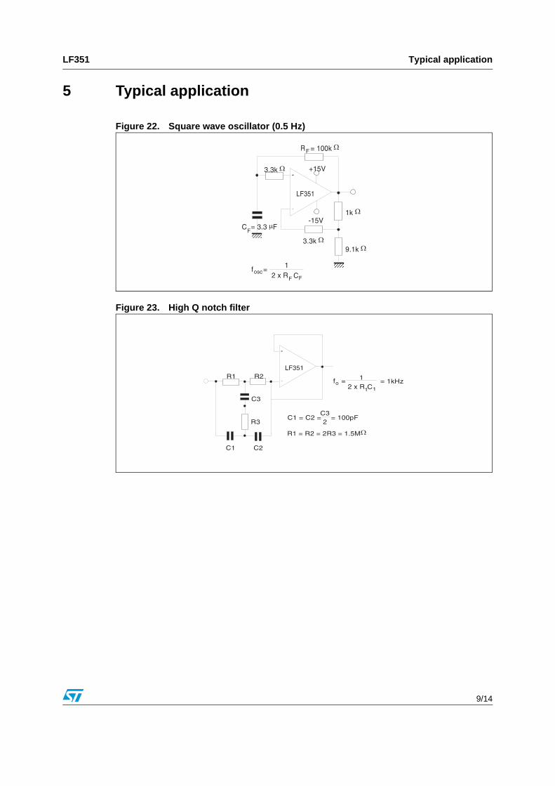
Figure 22. Square wave oscillator (0.5 Hz)
Figure 23. High Q notch filter

Package information LF351
10/14
6 Package information
In order to meet environmental requirements, STMicroelectronics offers these devices in ECOPACK® packages. These packages have a lead-free second level interconnect. The category of second level interconnect is marked on the package and on the inner box label, in compliance with JEDEC Standard JESD97. The maximum ratings related to soldering conditions are also marked on the inner box label. ECOPACK is an STMicroelectronics trademark. ECOPACK specifications are available at: www.st.com.

LF351 Package information
11/14
6.1 DIP8 package information
Figure 24. DIP8 package mechanical drawing
Table 4. DIP8 package mechanical data
Ref.
Dimensions
Millimeters Inches
Min. Typ. Max. Min. Typ. Max.
A 5.33 0.210
A1 0.38 0.015
A2 2.92 3.30 4.95 0.115 0.130 0.195
b 0.36 0.46 0.56 0.014 0.018 0.022
b2 1.14 1.52 1.78 0.045 0.060 0.070
c 0.20 0.25 0.36 0.008 0.010 0.014
D 9.02 9.27 10.16 0.355 0.365 0.400
E 7.62 7.87 8.26 0.300 0.310 0.325
E1 6.10 6.35 7.11 0.240 0.250 0.280
e 2.54 0.100
eA 7.62 0.300
eB 10.92 0.430
L 2.92 3.30 3.81 0.115 0.130 0.150

Package information LF351
12/14
6.2 SO-8 package information
Figure 25. SO-8 package mechanical drawing
Table 5. SO-8 package mechanical data
Ref.
Dimensions
Millimeters Inches
Min. Typ. Max. Min. Typ. Max.
A 1.75 0.069
A1 0.10 0.25 0.004 0.010
A2 1.25 0.049
b 0.28 0.48 0.011 0.019
c 0.17 0.23 0.007 0.010
D 4.80 4.90 5.00 0.189 0.193 0.197
E 5.80 6.00 6.20 0.228 0.236 0.244
E1 3.80 3.90 4.00 0.150 0.154 0.157
e 1.27 0.050
h 0.25 0.50 0.010 0.020
L 0.40 1.27 0.016 0.050
k 1° 8° 1° 8°
ccc 0.10 0.004
LF351 Ordering information
13/14
7 Ordering information
8 Revision history
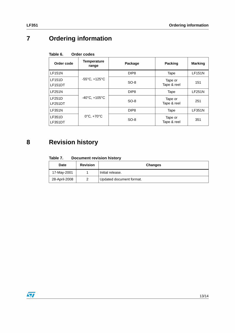
Table 6. Order codes
Order codeTemperature
rangePackage Packing Marking
LF151N
-55°C, +125°C
DIP8 Tape LF151N
LF151D
LF151DTSO-8
Tape orTape & reel
151
LF251N
-40°C, +105°C
DIP8 Tape LF251N
LF251D
LF251DTSO-8
Tape orTape & reel
251
LF351N
0°C, +70°C
DIP8 Tape LF351N
LF351D
LF351DTSO-8
Tape orTape & reel
351
Table 7. Document revision history
Date Revision Changes
17-May-2001 1 Initial release.
28-April-2008 2 Updated document format.
LF351
14/14
Please Read Carefully:
Information in this document is provided solely in connection with ST products. STMicroelectronics NV and its subsidiaries (“ST”) reserve theright to make changes, corrections, modifications or improvements, to this document, and the products and services described herein at anytime, without notice.
All ST products are sold pursuant to ST’s terms and conditions of sale.
Purchasers are solely responsible for the choice, selection and use of the ST products and services described herein, and ST assumes noliability whatsoever relating to the choice, selection or use of the ST products and services described herein.
No license, express or implied, by estoppel or otherwise, to any intellectual property rights is granted under this document. If any part of thisdocument refers to any third party products or services it shall not be deemed a license grant by ST for the use of such third party productsor services, or any intellectual property contained therein or considered as a warranty covering the use in any manner whatsoever of suchthird party products or services or any intellectual property contained therein.
UNLESS OTHERWISE SET FORTH IN ST’S TERMS AND CONDITIONS OF SALE ST DISCLAIMS ANY EXPRESS OR IMPLIEDWARRANTY WITH RESPECT TO THE USE AND/OR SALE OF ST PRODUCTS INCLUDING WITHOUT LIMITATION IMPLIEDWARRANTIES OF MERCHANTABILITY, FITNESS FOR A PARTICULAR PURPOSE (AND THEIR EQUIVALENTS UNDER THE LAWSOF ANY JURISDICTION), OR INFRINGEMENT OF ANY PATENT, COPYRIGHT OR OTHER INTELLECTUAL PROPERTY RIGHT.
UNLESS EXPRESSLY APPROVED IN WRITING BY AN AUTHORIZED ST REPRESENTATIVE, ST PRODUCTS ARE NOTRECOMMENDED, AUTHORIZED OR WARRANTED FOR USE IN MILITARY, AIR CRAFT, SPACE, LIFE SAVING, OR LIFE SUSTAININGAPPLICATIONS, NOR IN PRODUCTS OR SYSTEMS WHERE FAILURE OR MALFUNCTION MAY RESULT IN PERSONAL INJURY,DEATH, OR SEVERE PROPERTY OR ENVIRONMENTAL DAMAGE. ST PRODUCTS WHICH ARE NOT SPECIFIED AS "AUTOMOTIVEGRADE" MAY ONLY BE USED IN AUTOMOTIVE APPLICATIONS AT USER’S OWN RISK.
Resale of ST products with provisions different from the statements and/or technical features set forth in this document shall immediately voidany warranty granted by ST for the ST product or service described herein and shall not create or extend in any manner whatsoever, anyliability of ST.
ST and the ST logo are trademarks or registered trademarks of ST in various countries.
Information in this document supersedes and replaces all information previously supplied.
The ST logo is a registered trademark of STMicroelectronics. All other names are the property of their respective owners.
© 2008 STMicroelectronics - All rights reserved
STMicroelectronics group of companies
Australia - Belgium - Brazil - Canada - China - Czech Republic - Finland - France - Germany - Hong Kong - India - Israel - Italy - Japan - Malaysia - Malta - Morocco - Singapore - Spain - Sweden - Switzerland - United Kingdom - United States of America
www.st.com