Embed Size (px)
Citation preview

***** Copyright © EQuestionAnswers.com *****

Wireless Data/Voice TransceiverAn Electronic Project
Index Subjects PagesIntroduction 3Theory Amplifiers Using IC-741 Op-Amp 4 555 Timer & Related Theory 6 Modulation Techniques 11 Analog modulation, Digital modulation FM Modulation & Demodulation 14
Tuned Collector OscillatorFM TransmitterF M Demodulation Using PLL
ASK Generation & Detection 18ASK Generation using 555 TimerASK Detection Using Comparator
Radiation, Antennas and Electromagnetic wave Propagation 20Concept of antenna, Dipole, Folded Dipole and Monopole Antenna Propagation of Electromagnetic wave
Audio Accessories 26Loud speaker & MicrophonePre- Amplifier & Beep Tone Generator
Audio Power Amplifier 28 Regulated Power Supply 31Design Consideration
32 Selection & CalculationsBlock Diagram & Operations
34 Block Diagram,Circuit operation of Transmitter & ReceiverExperimental Results
36 Signals Observed in CROManufacture’s Specifications
37Data Sheets
39555 Timer741 op-ampTBA 810 power amp
Conclusion 45Advantage
***** Copyright © EQuestionAnswers.com *****

DisadvantageFuture aspectsAcknowledgement
Reference 46
***** Copyright © EQuestionAnswers.com *****

In present situation digital signal transmission is an upcoming technology. In mobile, Satellite communication, CATV, or Optical fiber communication everywhere we use digital modulation. In our project our aim is to design a voice data transceiver based on FM and ASK modulation.
Analog signal can be sent to a distance via a
transmitter. Transmitter may be an AM or FM type. In our project we use FM transmitter as it gives most noiseless performance and robust in construction. A simple one transistor tuned collector oscillator is used for the transmitter. We can send voice signal directly collected from a microscope. In case of digital signal we cannot transmit it directly as it has some D.C. component in it. We have an Ask section where we modulate the digital bit stream into ASK signal and send the ASK signal via this transmitter.
In the demodulation part we use a PLL FM detector.
PLL has the optimum performance as a FM detector. After demodulation we get the base-band signal back. Voice signal are obtained after PLL demodulation. We have to amplify with a Power amplifier and then fed to a Loud Speaker. In case of digital signal after PLL demodulation we get ASK signal back. Now ASK demodulator is used to demodulate the digital signal.
In the following section we present the detailed theory
of every fields related to the project and basic block diagram construction with functions of every units. Then the design part is given where we put every details of
***** Copyright © EQuestionAnswers.com *****

how we design the circuit and every necessary calculation. In the experimental part we list all the values, which we get after testing the circuit. Then we attach all the data-sheets of the integrated circuits. In the conclusion some advantages, disadvantages and some possible fields of application of this project are discussed.
AMPLIFIERS USING IC-741 OP-AMP
INVERTING AMPLIFIER ::
A basic inverting amplifier can be made using an op-amp connected with an input resistance R1 and a feedback resistance Rf. Since Rf connects the output terminal to the inverting input terminal, it provides a –ve feedback .The non-inverting input terminal is grounded. The input and output voltages are V 1 and V0, respectively. Let V =Vin be the voltage at the inverting input terminal. As the open-loop gain A of the op-amp is very high and the output voltage V0 is finite due to –ve feedback, we have,
V = AV0
; as Và0 as A
àinfinity.Therefore, the inverting input terminal (G) is practically at the ground potential. Thus, though the point G is not actually connected to ground. It is held virtually at ground potential, whatever be the magnitudes of V1 and V0.
The current through the resistance R1 is, I 1
1
RV)-(V
Assuming that the op-amp is an ideal one with infinite input impedance, the current I passes through R f
and not into the op-amp. Kirchhoff’s current law when applied at the point G gives,
f
0
1
1
R)V-(V
R
V)-(V
***** Copyright © EQuestionAnswers.com *****

Inverting Amplifier
As the point G is a virtual grounded, V ~ 0.Hence f
0
1
1
RV-
RV
.
Thus closed - loop voltage gain of the Inverting Amplifier is given by,
1
f
1
0
RR
- VV
The –ve sign signifies that the output voltage is inverted with respect to the input voltage. The input resistance of the amplifier system is
Rin = IV1
= 1
11
1
V)/R-V (V R
NON-INVERTING AMPLIFIER ::
A basic non-inverting amplifier can be made using an op-amp connected with an input resistance R1 and a feedback resistance Rf .The input voltage V1 is applied to the non-inverting terminal. Since the voltage gain of the op-amp is infinite, the potential of the inverting point is also V1.The current flowing into the op amp is negligible as its input impedance is very large. Hence, applying Kirchhoff’s current law at the inverting point we obtain,
***** Copyright © EQuestionAnswers.com *****

Non-inverting Amplifier
Voltage Follower
1
1
f
10
RV
R)V-(V
or, 1
f
1
0
RR 1
VV
Which is the voltage gain of the amplifier system. As the gain is +ve, there is no phase difference between the input voltage V1 and output voltage V0. Voltage follower is one special configuration of
Non-inverting amplifier. Where Rf=0 and R1=infinity, so 1
VV
1
0
, Hence the output of the amplifier follows exact the input voltage or output follows the input voltage.
555 Timer & Related Theory
ASTABLE MULTIVIBRATOR USING 555 TIMER ::
A multivibrator is a relaxation oscillator generating nonsinusoidal waveforms. Basically, the multivibrator is a two-stage amplifier or oscillator operating in two modes or states. Each amplifier stage feeds back the other such that the active element of one stage is driven to saturation and the other to cut off. A new set of actions, producing the opposite effects, then follows. Thus the saturated stage becomes cut off and the cut off stage saturates. The operation of the multivibrator is based on the fact that no two active elements have exactly identical characteristics. The NE 555 is a widely used IC timer, a circuit that car run in either of two modes:- Monostable and Astable.In the astable mode, it can produce regular waves with a variable duty cycle. The 555-timer chip has the following components:
1. A voltage divider. 2. Two comparators 3. An R-s flip-flop
***** Copyright © EQuestionAnswers.com *****

4. An n-p-n transistor.
Block diagram representation of the 555 timer circuit.
OPERATION :: In astable operation the 555 timer has no stable states, which means that it cannot remain indefinitely in either state i.e. it oscillates when operated in the astable mode and it produces a rectangular output signal. Since no input trigger is needed to get an output, the operating in the astable mode is sometimes called Free-Running Multivibrator. Here we need two external resistors and one capacitor to set the frequency of operation.
***** Copyright © EQuestionAnswers.com *****

Figure above shows an astable multivibrator implemented using the 555 IC together with an external resistor RA , RB and an external capacitor C.
1-Initial State S=1 R=0 ® Q=1 Q.=0 (C begins to charge) Initially capacitor is discharged or empty. At this time VTH > VC causes output of the
***** Copyright © EQuestionAnswers.com *****

comparator 1 to be 0 so R=0 and VTL > VC causes output of the comparator 2 to be 1 so S=1. For S=1 and R=0 , Q=1(high,Vcc) and Q.=0(low,0V).Thus Vo is high and transistor is OFF. Capacitor C will charge up through the series combination of RA and RB , and the voltage across it , Vc , will rise exponentially toward Vcc. 2- Vc = VTL , comparator 2 ® Low S=0 R=0 ® Q=1 Q.=0 (no change , C is still charing) As Vc crosses the level equal to VTL , the output of the comparator 2 goes low.(Vc = VTL ,
comparator 2 ® Low ). This however has no effect on the circuit operation because this will make the inputs of the flip-flop as S=0 and R=0 (no change state) which means outputs of flip-flop will remain same. This state continues until Vc reaches and begins to exceed the threshold of comparator 1, VTH.
3- Vc = VTH , comparator 1 ® High S=0 R=1 ® Q=0 Q.=1 (C begins to discharge ) When Vc reaches and begins to exceed VTH , the output of the comparator 1 goes high and resets the flip flop( S=0 R=1 ® Q=0 Q.=1).Thus Vo goes low , Q. goes high and so transistor is turned ON. The saturated transistor causes a voltage of approximately 0V to appear at the common node of RA and RB.Thus C begins to discharge thru RB and the collector of the transistor. Note that R = 1(flip-flop input) for a very short time.
4- Vc = VTH , comparator 1 ® Low S=0 R=0 ® Q=0 Q.=1 (no change , C continues to discharge )
VC will drop again below VTH immediately after discharging process is started.S=0 and R=0 will not affect the system(no change state) The voltage Vc decreases exponentially with a time constant RB.C toward 0V.This state will continue until Vc reaches VTL. 5- Vc = VTL , comparator 2 ® High S=1 R=0 ® Q=1 Q.=0 (C begins to charge ) When Vc reaches the threshold of comparator 2 , VTL , the output of comparator 2 goes high and then S=1 R=0 causes Q=1 and Q=0.Thus output Vo goes high and Q. goes low , turning off
the transistor. Capacitor C begins to charge through the series equivalent of RA and RB , and its voltage rises exponentially toward Vcc with a time constant (RA+RB).C.This rise continues until Vc reaches
VTH, at which time the output of comparator 1 goes high , resetting the flip-flop , and the cycle goes on. Determinig the Period T =TH + TL: For TH:
From the general solution for step and natural responses : X(t) = XF + [ X(to) - XF].e-(t-t0) / i
Vc= Vcc+[ VTL Vcc/ ior ; VC = (Final Val . Initial Val) ( 1- e-t /RC ) + shifting Vc = (b-a) ( 1- e-t /RC ) + a
***** Copyright © EQuestionAnswers.com *****

Vc= (Vcc)(1- / i ) +VTL Vc= (Vcc)(1- / i ) +VTL is equal Vc= Vcc+[ VTL Vcc/ iwhere i =(RA + RB).C
Substituting t=TH VC=VTH=2/3Vcc and VTL=1/3Vcc in the equation Vc= (Vcc)(1- / i ) +VTL
32
Vcc=( Vcc - 31
)(1- / i ) + 31
Vcc where i =(RA + RB).C
e-t/i= 2
1
TH = (RA+RB).(C).(ln2) TH = 0.69(C)(RA+RB) For TL:
X(t) = XF + [ X(to) - XF].e-(t-t0) / i
Vc= 0 V+[ VTH/ i
Vc = VTH. e-t / i where i =RB.C For t=TL VC=VTL=1/3Vcc and VTH=2/3Vcc Vc = VTH. e-t / iwhere i=RB.C 1/3Vcc=2/3Vcc. e-t / i TL = RB.C.ln2 TL = 0.69RB.C T = TH + TL
T = 0.69(C)(RA+RB) + 0.69RB.C T = 0.69.C.(RA + 2RB)
***** Copyright © EQuestionAnswers.com *****

Also the duty cycle of the output square wave can be found as:
Duty Cycle= LH
H
TTT = BA
BA
RRRR
2
Note that the duty cycle will always be greater than 0.5(50%).It approaches to 0.5 if RA isselected much smaller than RB.
Modulation Techniques
When we wand to communicate to some one, we have some message to tell another. In technological point of view this message may be a base-band voice or audio, video and even may be digital bits from computer. To send these messages we must have some communication channel like wires, Co-Axial cable, even wireless radio waves, microwaves or infrared. We can easily transmit messages through wires or cables. But when we want to transmit a Voice or Video through wireless media some problem comes. Because Voice or video signals have a definite bandwidth, if we directly transmit it we cannot receive it properly. Voice signal has lower Bandwidth therefore it will not propagate through space and will be attenuated. To transmit voice signal a large size antenna is required as antenna length is proportional to half of wavelength. The size of the antenna will be more than the distance between transmitter and receiver. Again when more than one transmitter is involved all station will overlap in one frequency band.
For those above reasons we choose a carrier, which is a high frequency radio wave, can travel long distance without attenuation and as the frequency is high smaller antenna is required. Selecting different carrier frequency for different transmitting stations can eliminate overlapping of frequency band.
Analog Modulation:
***** Copyright © EQuestionAnswers.com *****

Now we have to develop some way to send the information of message signal via this carrier signal. The carrier signal is a high frequency sinusoidal signal represented by amplitude, frequency and phase. We can vary one of this parameter accordingly with the message information. This operation of varying amplitude, frequency or phase of carrier signal accordingly with the instantaneous amplitude of the message signal is called modulation.
There are three basic types of analog modulations. 1. AM or Amplitude Modulation2. FM or Frequency Modulation3. PM or Phase modulation
FM and PM can be called angle modulation as a whole.AM or amplitude modulation is the process of varying the instantaneous amplitude of Carrier
signal accordingly with instantaneous amplitude of message signal. Thus, if m(t) is the message signal and c(t)=Acoswct then AM signal F(t) is written as
F(t)= Acoswct+m(t) coswctF(t)=[A+m(t)] coswct
AM is the simplest type of modulation. Hardware design of both transmitter and receiver is very simple and less cost effective.
FM or Frequency modulation is the process of varying the in instantaneous frequency of Carrier signal accordingly with instantaneous amplitude of message signal. Thus, if m(t) is the message signal and c(t)=Acoswct then FM signal will be
F(t)= Acos(wc t+
t
f dmk
)()
PM or Phase modulation is the process of varying the instantaneous phase of Carrier signal accordingly with instantaneous amplitude of message signal. Thus if m(t) is the message signal and c(t)=Acoswct then FM signal will be
F(t)= Acos(wct+kpm(t))
Digital modulation:Digital modulation in somewhat similar to the analog modulation except base band signal is of
discrete amplitude level. For binary signal it has only two level, either high or logic 1 or low or logic 0. The modulation scheme is mainly three types.
1. ASK or Amplitude shift Key2. FSK or Frequency shift key3. PSK or Phase shift key
ASK or Amplitude shift Key:
When the carrier amplitude is varied in proportion to message signal m(t). We have the modulated carrier m(t)coswct where coswct is the carrier signal. As the information is an on-off
***** Copyright © EQuestionAnswers.com *****

signal the output is also an on-off signal where the carrier is present when information is 1 and carrier is absent when information is 0. Thus this modulation scheme is known as on-off keying (OOK) or amplitude shift key.
FSK or Frequency shift key:
When Data are transmitted by varying frequency of the carrier, we have the case of frequency shift key. In this modulation carrier has two predefined frequency wc1 and wc2. When information bit is 1 carrier with wc1 is transmitted i.e. coswc1 and When information bit is 0 carrier with wc0 is transmitted i.e. coswc0
PSK or Phase shift key:
The phase of the carrier is shifted for this modulation. If the base band signal m(t) =1 carrier in phase is transmitted. If m(t)=0 carrier with out of phase is transmitted i.e. cos(wct+p). If phase shift is done in 4 different quadrants then 2bit of information can be sent at a time. This scheme is a special case of PSK modulation known as QPSK or Quadrature Phase Shift Key.
Here is the wave form of ASK and FSK signal:
***** Copyright © EQuestionAnswers.com *****

FM Modulation & Demodulation
TUNED COLLECTOR OSCILLATOR ::
***** Copyright © EQuestionAnswers.com *****

An oscillator is a system consisting of active and passive circuit elements to produce a sinusoidal or other repetitive waveforms at the output without the application of an external input signal. The function of an oscillator is to convert DC power into AC power. In an oscillating circuit the amplitude of voltage or current oscillation decays with time owing to the dissipation of energy in the resistance contained in the circuit. If a –ve resistance is incorporated in the circuit to generate energy that compensates for the loss of energy through the passive resistance, oscillations with undiminished amplitude can occur. Basically therefore a –ve resistance must be provided in an oscillator. This is accomplished in a feedback oscillator by providing an external +ve feedback to make the overall gain infinite. The initial signal to trigger the oscillation is obtained from the noise voltage, which is produced from the power supply of the system. The frequency spectrum of noise being very wide it always has a voltage component at the frequency required for the oscillation. So the primary requirements of a feedback oscillator are: -
1. An amplifier with external regenerative feedback to give a –ve resistance in the system.2. A frequency determining networks to produce oscillation of the desirable frequency.3. Some system non-linearity to limit the amplitude of oscillation.4. A DC Power source to supply the energy.
Tuned Collector Oscillator is a LC feedback oscillator. Here we use a transistor in CE configuration which gives 180 degree phase shift between its input and output voltage. Also we use a transformer, which gives another 180-degree phase shift needed for oscillation. The frequency determining circuit is made up bye the capacitor C together with the transformer primary inductance L. The LC tuned circuit connected to the collector accounts for the name ‘Tuned Collector Oscillator’. The LC tuned circuit is called tank circuit because this circuit determines the frequency of oscillation. There is a large value of resistance called R2 connected in series with the transformer secondary winding. The main purposes served by R2 are to: -
1. Reduce the loading of the collector circuit by the low input resistance of the transistor.2. Introduce regenerative feedback just require to sustain oscillations.3. Decrease the input non-linear distortion.4.The frequency of oscillation is approximately given by the natural resonant frequency of the LC tank circuit. Thus
FM TRANSMITTER::
***** Copyright © EQuestionAnswers.com *****

A FM transmitter is usually a VHF tuned collector oscillator with center frequency
. Frequency range is around 80-108Mhz. We can choose value of L or C
such that center frequency can be changed between the frequency band. Usually 30-300Mhz VHF range is optimal for FM TRANSMITTER. Transmitter is a combination of an oscillator, Modulator and a suitable Antenna system. Carrier is generated in the oscillator. Then it is modulated with the information signal then transmitted through transmission channel via an interface of antenna system. Antenna system converts the carrier current to electromagnetic waves, which easily travels through the space.Now we consider our circuit. The CE mode transistor is a tuned collector with a tuned LC circuit. The center frequency of oscillator is determined by this LC value. The center
frequency is thus . Now we go in to the modulation part. When a signal is
applied in to the base, the base–emitter (B-C) voltage is changed. The voltage across the varactor diode also changed. The capacitance of base to emitter junction also changed. This capacitance falls series with the tank circuit. The operating frequency also changed. Thus the change of frequency is achieved which is the main criteria of FM modulation.The change of frequency should not be such that it can track by a PLL. The FM wave is now coupled with a telescopic antenna for broadcast.
VHF oscillator and FM Transmitter
***** Copyright © EQuestionAnswers.com *****

FM DEMODULATION USING PLL ::
In FM modulation when the bandwidth becomes so large that the input noise power is relatively large, the performance of the FM system degrades rapidly and the system exhibits a threshold. When input noise power is quite large we would be inclined to use FM and allows a sacrifice of bandwidth for the sake of improved output signal-to-noise ratio. But FM threshold prevents such use of FM.Conventional FM discriminators does not occur threshold improvement while FM demodulator using Phase-Locked Loop (PLL) improves threshold.
DEFINITION OF PLL :: The Phase-Locked Loop (PLL) is a feedback system that may be used to extract a base band
signal from a FM carrier, especially under low SNR conditions. Thus PLL tracks the phase and the frequency of the carrier component of an incoming signal.
A PLL has three basic components: -1. A voltage-controlled oscillator (VCO)2. A multiplier, serving as a phase detector or a phase comparator3. A loop filter having response H(s)The operation of PLL is similar to that of a feedback system except that the quantity feedback and
compared is phase, but not amplitude.
OPERATION OF VCO :: An oscillator whose frequency can be controlled by an external voltage is a Voltage Controlled
Oscillator (VCO). In a VCO, the oscillation frequency varies linearly with the input voltage. If a VCO input voltage Eo(t), its output is a sinusoid of frequency given by,
ωVCO = ωc + Ceo(t)Where C is a constant of the VCO and ωc is the free-running frequency of the VCO. The multiplier
output is further low pass filtered by the loop filter and then applied to the input of the VCO. This voltage changes the frequency of the oscillator and keeps the loop locked, i.e. the frequency and phase of the input and output sinusoidal signals becomes identical.
***** Copyright © EQuestionAnswers.com *****

OPERATION OF PHASE COMPARATOR :: A Phase Comparator is a device with two input ports and a single output port. If periodic signals of identical frequency but with a timing difference are applied to the inputs, the output is a voltage, which depends on the timing difference. After phase comparator the signal is low pass filtered to get the error voltage.
PLL ACTING AS A DEMODULATOR ::In PLL the output Eo(t) of the loop filter H(s) acts as an input to the VCO. The free-running frequency of
the VCO is set at the carrier frequency ωc. The instantaneous frequency of the VCO is given by, ωvco =ωc + Ceo(t) ---------(1)If the VCO output is, Bcos [ωct + θo(t)], then its instantaneous frequency is
[ωc + o(t)]. Therefore,
o(t) = Ceo(t) ----------(2), where C and B are constants of the PLL.
Let the incoming signal be, Asin [ωct +θi (t)]. At the multiplier this incoming signal and the VCO output are fed so that the output X(t) is given by,X(t) = A B sin(ωct +θi )cos(ωct +θo)
=[ AB {sin ( i - o) + sin(2ωct + i + o)}] ---------(3)The sum frequency term is suppressed by the loop filter, Hence the effective input to the loop filter is [
ABsin{ i (t) - o (t)}]. If h(t) is the unit impulse response of the loop filter,
eo(t) = h(t) * [ ABsin{ i (t) – o (t)}] = [ (AB)] h(t – x)sin[ i (t) – o (t)]dx -(4)
Substituting eq.(2) in eq.(4) we get o(t) = AK h(t – x)sin[ e(x)]dx ----------------(5)
where K = CB and e (t) is the phase error, defined as e(t) = i(t) – o(t).
When the incoming FM carrier is Asin[ωct + i (t)],
i(t) = kf m( )d -------------(6)
Hence,
eo(t) = [kf m( )d ] – 0e(t)and assuming a small error e(t) we get from eq.(2)
eo(t) = [ o(t)]~ kf m(t) ---------------(7)
Thus, the PLL acts as an FM demodulator.
***** Copyright © EQuestionAnswers.com *****

ASK GENERATION AND DETECTION
DEFINITION OF ASK ::In Amplitude Shift Keying (ASK), the amplitude A of the carrier signal Acos(ω ct) is switched
between the two levels, which correspond to the level of the input binary signal. The two levels of the binary signal can be 0 volt (Logic 0) and 1 volt (Logic1).
ASK GENERATION ::There are two methods of generating ASK signals.
First Method :-
In ASK generation, the base band signal Fb (t) is multiplied by any periodic signal S(t) so that the result is as follows: -x(t) = Fb (t)S (t) The product x(t) contains a series of AM waves with carrier frequencies that are harmonic multiples of the fundamental frequency fc. A band pass filter is used to extract any of the harmonics, thus generating the ASK signal.
Second Method :-
The second form of ASK modulator utilizes a square law device which may be a diode. Here the base band signal is added to the carrier oscillations and squaring the sum gives the cross product, which is the desired modulation term. That is
[ Fb(t) + COS ωct ]2 = Fb (t)2 + COS ωct + 2Fb (t)COS ωct
ASK Generation Using 555 Timer
Simple ways to generate ASK signal is using 555 timers as an Astable mode. The RC network (RA,RB and C) will determine the Carrier frequency( i.e. T =1/f= 0.69.C.(RA + RB) ) of ASK. The principle is very simple. Pin No. 4 of 555 timer is RESET bar. That means if this PIN is high the IC will be activated. Other wise if this pin is grounded output will be absent. Thus Appling the message information in 4th pin we can get ASK signal.
ASK DETECTION ::
***** Copyright © EQuestionAnswers.com *****

ASK detection can be of two types, either coherent or incoherent. Coherent demodulators maintain precise timing (phase) of the incoming carrier. Incoherent demodulators do not maintain this phase and essentially perform a non-linear operation on the modulating signal to retrieve the base band amplitude.
First Method :-The synchronous demodulator is an example of Coherent Detection. It simply retranslates the
frequencies of the incoming waveform down to the baseband. This is done by multiplying or heterodyning the incoming ASK waveform with a local oscillator matched to the carrier. The output of the multiplier is,
Fb (t) {[cos(ωct)]2} = 2(t) Fb
+ 2(2 (t)cos [Fb c tw
The low pass filter will remove the cos (2ωct) component. The output of the filter having response in ωc, which exactly matches that of the transmitter carrier oscillator.
Second Method :-
The square law demodulator is an example of Incoherent Detection. Here a square law device is used whose output is passed through a low pass filter. The output of the filter is then fed to a non-linear device to take its square root so that the base band amplitude is retrieved.
ASK Detection Using Comparator:
Comparators are Op-Amps operated is differential mode. One of the input terminal is kept at reference voltage and signal is applied at the other terminal. There are two type of comparator Positive and Negative comparator. If signal is applied to Non-inverting terminal then it is Positive comparator. Positive comparator gives high when signal level is greater than reference voltage. If signal is applied to inverting terminal then it is Negative comparator. Negative comparator gives high when signal level is less than reference voltage. The operation of comparator is simple. It either works in Inverting (Positive comparator) or Non-Inverting mode (Negative comparator) with very high feed-back resistance means very high gain i.e. either is Positive saturation or Negative saturation.
In our project we uses simple envelope detector followed by three-stage magnitude comparator and a level translator. After the envelope detection signal is fed to three-stage magnitude comparator. Three-stage comparator
***** Copyright © EQuestionAnswers.com *****

is used for reliable signal detection and noise rejection. At the last stage a level translator is used to get output voltage in unipolar or bipolar mode.
Radiation, Antennas and Electromagnetic wave Propagation
In radio communication system the receiving antenna is linked to the transmitting antenna through the electromagnetic wave. This arrangement is somewhat similar to that we find in transformer circuits. In the case of transformer, the coupling is strong and the field involved is entirely magnetic. In the case of antenna, however, the coupling is weak and the field involved is electromagnetic.
The antenna coupling system can be represented by a four terminal network. This representation is very useful because we can then apply the well-known network theorems to solve antenna problems. The important general results obtained there by are applicable to all kinds of antennas. A network theorem which is particularly useful in antenna theory is the reciprocity theorem.
Fig shows a high frequency generator, connected to a two parallel wire transmission line. If the line is kept sufficiently far away from any metallic or conducting objects, equal and opposite current will flow in the two wires at any given position on the line. Therefore, at any appreciable distance, from the line, the field effects of two wires will almost cancel each other. The end of the line, remote from the generator, is sorted with a straight segment of wire. The field effect of this wire may be observed at any distance remote from the line, because there is no source of equal and opposite fields to cancel them.
This shorted segment is known as elemental antenna.Radiation resistance:
When a high frequency current flows through an antenna, there is also an energy-loss due to the radiation of electromagnetic energy. This in turn, concludes that the transmission line, feeding the elemental antenna, must see a resistance component of load. If the load were all-resistive, the average power delivered to the antenna would have to be zero. It is un-important that our energy is not dissipated as heat. There is still an energy-loss to be accounted for and the amount of energy lost is given by
022)(789 IdlPavg
or
rmsavg IdlP 22)(789
or
202
1 IRP radavg
The radiation resistance of elemental antenna is 2)(789
dlRrad
Antenna Directivity And Gain:Directivity and gain is two very useful terms in Antenna System. For a particular direction the ratio of power
per unit solid angle to the power per unit solid angle for a Reference isotropic antenna is called the Directivity.
***** Copyright © EQuestionAnswers.com *****

Gain is the ratio of maximum radiation intensity of an antenna to the maximum radiation intensity of a reference antenna provided both antennas have the same power input.
Polarization:Polarization is the direction of electric field of the incoming electromagnetic waves.
The Half-Wave Dipole
There is only one part of a receiving aerial that is active, i.e. does the receiving and is connected to the TV/radio set. This active element is called the dipole. The simplest design of antenna would consist of a dipole only:
A half-wave dipole
In the diagram above, there are two wires marked 'to receiver.' For UHF and VHF, one wire will be the copper-core and the other the copper braiding of a co-axial cable.
Before we precede, a quick word about gain. Although having a technical definition, for us 'gain' can mean "the effectiveness with which a receiving aerial receives a signal."
The diagram below shows the reception pattern of a half-wave dipole. The blue area is where the gain is higher than a certain value; the dipole is in the center:
***** Copyright © EQuestionAnswers.com *****

We can change the directivity of the aerial by adding other elements. Any other elements that we add to the basic half-wave dipole are called passive elements and are not connected electrically to the dipole.
There are two types of passive elements:
Directors
Directors alter the directivity of the aerial so that the aerial's gain is improved in front of the dipole. Most aerials have more than one director, and the more directors the aerial has the better the aerial is at picking out the signal from the required source and rejecting signals from other angles.
These diagrams do not show the cross-bar that holds all the elements in place as it does not much affect the characteristics of the aerial.
The spacing between the directors, diameter of the tubing used and the spacing between the first director and the dipole are important in practice but will be disregarded here. The length of the directors governs the bandwidth of the aerial (over which channels it is effective), but suffice it to say that it is about 75% the length of the dipole.
The gain of the dipole with directors in place looks like this:
Notice how the gain is now more focused in the direction of the directors.
***** Copyright © EQuestionAnswers.com *****

As stated earlier, the more directors an aerial has the more focused the gain is in the direction of the directors. Every new director added becomes less effective though, and in practice it is only worth adding 18-20 directors to the aerial, as any more than this wouldn't increase the gain very much.
On the diagram above, the aerial still has some gain at the rear - in other words, it can still receive signals from behind. This is known as a low front-to-back ratio.
The Reflector
To improve the front-to-back ratio we can add the second type of passive element, a reflector. The reflector reflects signal coming in from the back of the aerial whilst improving the forward gain.
This design is called a Yagi-Uda array, after its creators.
Again, the length, size and position of the reflector affect the aerial's properties, but we won't go into that here.
The reflector can take the shape of a metal plate (with holes in it, making the aerial more impervious to wind) or several rods spaced equidistant from the center of the dipole.
The result is that there is less gain behind the aerial and more, where we want it to be, in front:
***** Copyright © EQuestionAnswers.com *****

Folded DipolesIn order to minimize signal loss it is important that the impedance (a sort of resistance for
AC) of the dipole matches that of the feeder cable and the receiving set.
The impedance for the type of dipole discussed above is about 75 ohms. More often than not though the impedance needs to be altered to match the cable and receiving set characteristics.
This change of impedance is achieved by folding a rod over so that its folded length is still half-a-wavelength:
Now we know what each constituent part of an aerial is called and what its function is, let's look at some examples in the field.
Monopole Antenna:Consider a transmitter perpendicular to the ground. The electrons in the antenna, when a signal is
applied, are changing their velocities continuously (i.e. moving up and down very quickly) in response to the applied signal.
For a station that broadcasts at a wavelength of 1500m, the antenna needs to be 750m long. This is because there is a 'virtual antenna' caused by the aerial being earthed in the ground:
***** Copyright © EQuestionAnswers.com *****

The transmitting aerial (and the receiving aerial) need only be half-the-wavelength tall.
Now if this transmitter has no directional properties (i.e. it radiates in all directions equally), it has a coverage area, assuming completely flat ground that is a perfect circle:
(View from above - antenna in center; blue is coverage area)
Electromagnetic wave propagation
Different mechanisms are involved in the propagation of radio waves from transmitting to receiving antennas, the important ones being:
1. Ground wave or Surface wave propagation2. Space wave or Tropospheric wave propagation3. Sky wave or Ionospheric wave propagation
Ground wave or Surface wave propagation:***** Copyright © EQuestionAnswers.com *****

Due to the presence of the ground, near the transmitting and receiving antennas, the propagation of the ground waves takes place along the surface of the earth. In the case of long and medium wave signals, the ground wave propagation is common. Daytime reception of all radio signals is possible due to the ground wave propagation.
Space wave or Tropospheric wave propagation:The portion of the earth’s atmosphere situated in the first 15 km adjacent to the earth’s surface is
known as the earth’s Troposphere. The propagation of the space wave takes place through the earth’s troposphere. In case of radio waves from television, radar and frequency modulated transmitter, where the frequencies are above 50Mhz, the tropospheric space waves are the important means of radio communications.
Sky wave or Ionospheric wave propagation:An ionized region situated at height of 90km or more is known as the “Ionosphere”, which
contains electrons, positive ions and neutral atoms. The sky wave propagation takes place due to reflection of the radio wave from the lower surface of the ionosphere and earth’s surface. All long distance radio communications are possible due to the sky wave reflection from the ionospheric and as well as reflection from the satellites.
Audio Accessories
Theory of loud-speaker and Head-phone ::
Loudspeaker and Headphone works in the same principle of converting electrical signal to sound waves. We now discuss the basic construction of these transducers. It has a permanent magnet inside and some cupper coil around the magnet. The coil is attached to a diaphragm. The diaphragm is like a dish like shape and supported by a metal frame. Now when alternating audio signal is flowing through the coil, makes a alternating magnetic field. This alternating field, which is created in coil, interacts with the field of permanent magnet. Thus a force is created which makes vibration in the coil which intern vibrates the diaphragm. This vibration falls in the audio frequency. Thus sound is produced.
Theory of Microphone ::
***** Copyright © EQuestionAnswers.com *****

Microphone is a transducer, which converts the sound energy to electrical currents. Microphone may be of two type 1) Magnetic type and 2) Carbon type.Magnetic type microphones are similar structure to that of a headphone or loudspeaker. It has a permanent magnet inside and some cupper coil around the magnet. The coil is attached to a diaphragm. The diaphragm is like a dish like shape and supported by a metal frame. Here sound waves make vibration in the diaphragm. As coil is attached to it, it also vibrates. We know a moving coil in a magnetic field produces a current in it according to the law of generator. Thus a alternating audio current is produced in the microphone.Another type of microphone is the carbon type. It consists of a diaphragm and some carbon granules. The diaphragm is attached with the carbon. The two electrical terminals are connected in the carbon. A sound wave makes vibrations in the diaphragm and the diaphragm either makes some pressure or release pressure in the carbon according to the intensity of sound. The resistance of the carbon is dependent on the pressure on it. Application of pressure in carbon decreases its resistance and releasing in pressure increases the resistance. If microphone is connected with a resistance an some bias is applied, and sound is applied to it, there will produce some alternating current
Microphone Preamplifier:
The audio signal generated by a microphone is very weak. It must be preamplified to give it sufficient gain so that it can be fed to a transmitter. The unit has a operational amplifier in inverting mode.
***** Copyright © EQuestionAnswers.com *****

Beep Tone Generator:
Beep tone generator has three 555 Timer in Astable mode. Beeps are generated in 1s of time interval and stays for 350ms. In this 350ms two beeps are generated in 50ms interval and stays for 150ms each. Thus a twin tone just like a Mobile Telephone ring. The RC value in the timer is selected such that these three timers do the job for us. The first timer gives a on time of 350ms and off time of 1s. then in 350ms the second timer gives 150ms on then 50ms off then 150ms on. Thus the third timer which makes tone delivers two beeps in short time of 350ms and kept silent for 1s.
POWER AMPLIFIERS DEFINITION ::
***** Copyright © EQuestionAnswers.com *****

Power amplifiers convert DC power from the supply source to AC signal power at the load. Power amplifier seeks to supply power to a load such as a loudspeaker or a radio antenna. Thus, power amplifiers constitute the last stage of a radio receiver feeding the loudspeaker, or the last stage of a transmitter connected to the transmitting antenna. A special bipolar transistor called power transistor is used as the active amplifying element in a power amplifier. A power amplifier handles a large signal and the excursion of the operating point may go beyond the linear region of the amplifier active device characteristics. The efficiency of a power amplifier is the ratio of the AC output power to the power delivered by the supply source.
CLASSIFICATION ::
Power amplifiers are classified according to the method of operation. The position of the operating point (Q- point) and the portion of the characteristic curve that is used, determine the method of operation. They are classified as::
1. Class A2. Class B3. Class AB4. Class C 5. Class D amplifiers.
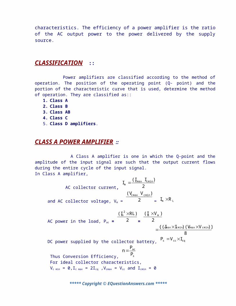
CLASS A POWER AMPLIFIER ::
A Class A amplifier is one in which the Q-point and the amplitude of the input signal are such that the output current flows during the entire cycle of the input signal.In Class A amplifier,
AC collector current, 2)I (I
I min cmax cm
and AC collector voltage, Vm =
2)V (V min cmax c
= R I Lm
AC power in the load, Pac = 2RL) (I 2 m
= 2)V (I mm
8)}V )(VI {(I min cmax cmin cmax c
DC power supplied by the collector battery, cqcc s I VP
Thus Conversion Efficiency, s
ac
PP
n
For ideal collector characteristics, Vc min = 0,Ic max = 2Icq ,Vcmax = Vcc and Icmin = 0
Hence n = cccq
cccq
VI8VI 2
= 0.25
***** Copyright © EQuestionAnswers.com *****

Hence the maximum efficiency obtainable from a Class A power amplifier, directly coupled to the load resistance, is 25%.
To avoid wastage of power and flow of DC component of current through the output device (e.g. voice coil of a loudspeaker) transformer coupling is used instead of direct coupling to the load resistance. In Transformer Coupled Class A power amplifier efficiency is 50%.CLASS B POWER AMPLIFIER :: When the operating point is at an extreme end of the load line such that the quiescent power is zero and the output current flows for just one half of the input signal cycle, the amplifier is said to be a Class B amplifier.
For PUSH PULL Class B power amplifier,
Total AC power output, P ac(tot) = L
cc
R 2
2V
Total DC power supplied by the source, P dc(tot) = (2Vcc2)/(ΠRL’)
Where RL’= 4Ra L
2
a = primary-to-secondary turns ratio of transformer
Thus Efficiency n = dc(tot)
ac(tot)
PP
= 0.785
Hence the maximum efficiency obtainable from a Class A power amplifier, directly coupled to the load resistance, is 78.5%.Without using a center-tapped output transformer, we can have a Class B power amplifier with push-pull output by employing complementary symmetry pair of transistors. Thus it is named as Complementary Symmetry Push-Pull Class B power amplifier. Here the input signal is coupled to the amplifier by an RC network.
CLASS AB POWER AMPLIFIER ::
When the operating point and the amplitude of the input signal voltage are such that the output current flows for more than one half cycle but less than one complete cycle of the input signal, the amplifier is termed as Class AB amplifier. A Class AB amplifier thus operates between the two extremes of Class A and Class B amplifiers.
CLASS C POWER AMPLIFIER ::
A Class C power amplifier is one in which the operating point is such that the output current flows for less than one half of the input signal cycle. The tuned circuit in the output of a Class C amplifier provides a full cycle of output signal for the fundamental or resonant frequency of the tuned circuit (LC tank circuit) of the output. This type of operation is therefore limited to use at one fixed frequency. The efficiency of a Class C power amplifier is 100%.
***** Copyright © EQuestionAnswers.com *****

CLASS D POWER AMPLIFIER ::
A Class D amplifier is designed to operate with digital or pulse-type signals. An efficiency of 90% is achieved using this type of circuit, making it quite desirable in power amplifiers.
7 W AUDIO POWER AMPLIFIER WITH THERMAL SHUT-DOWN: The TBA810 S is a monolithic integrated circuit in a 12-lead quad in-line plastic package, intended for use as a low frequency class B amplifier. The TBA810 S provides 7 W output power at 16 V/4 O 6 W at 14.4 V/4 8,2.5 W at 9 V/4 8, 1 W at 6 V/4 51 and works with a wide range of supply voltages (4 to 20 V); it gives high output current (up to 2.5 A), high efficiency (75% at 6 W output), very low harmonic and cross-over distortion. The circuit is provided with a thermal limiting circuit which fundamentally changes the criteria normally used in determining the size of the heat sink, in addition the TBA 810 S/AS can withstand short-circuit on the load for supply voltages up to 15 V.‚The TBA 810AS has the same electrical characteristics as the TBA 81OS, but its cooling tabs are flat and pierced so that an external heat sink can easily be attached.
Regulated Power Supply
***** Copyright © EQuestionAnswers.com *****

A regulated DC voltage source is obtained from a AC voltage source is easily by rectification. AC voltage is of 230V r.m.s. is easily available. This voltage is step downed by a transformer. Then rectified by diodes. If a center taped transformer is used only two diode is sufficient for full wave-rectification. If transformer is not a center taped bridge rectifier is used. After rectification the voltage is DC but contains high ripple. A LC or RC filter is used at the output to filter the high ripple voltage. Now this voltage can be used for DC supply. But this DC source is not regulated means if the input AC voltage changes output also changes. To get a regulated output zener diode regulation and Voltage Regulator may be used.
Voltage regulators come in integrated circuits in a variety of ranges. Regulators are of four types
1. Fixed output voltage regulators: positive or negative output voltage2. Adjustable output voltage regulators: positive or negative output voltage3. Switching regulators4. Special regulators
We use 7806 and 7812 for positive fixed Regulated power supply.
Block Diagram
Circuit Diagram
Design Consideration
Selection of Components:
***** Copyright © EQuestionAnswers.com *****

We select 555 timer and 741 Op-Amps as the circuit operations are known to us and easily available in the market. Selection of Modulation Scheme:
For analog transmission FM is the best choice as demodulation scheme gives most noiseless
output. PLL is used for demodulation. Now a days PLL comes in an IC which is not very costly but gives a better result. FM also is better than AM because of its bandwidth. For digital transmission we can provide more bandwidth thus more Baud Rate for Digital Transmission.
Again for Digital transmission we use ASK. As Frequency Modulator will modulate the signal we need not go for FSK. ASK circuitry is simple and less cost effective.Selection of Proper Transmission media:
Wireless transmission media has a wide range of bandwidth. In this band VHF band is most
Suitable for FM transmission. VHF ranges from 30-300 MHz. Lower side of the band is preferred for frequency stabilization. Up to 100MHz can be tuned by a LC tuned circuits where trimmer can be used as variable capacitor. Above that we have to use variable inductance, which is cost effective. So we select near 100MHz range.
Selection of Power Amplifier:
TBA 810 is a good Audio power amplifier. The size is less. No additional Heat sink is required. Frequency
response is good.Selection of PLL chip:
In the frequency Band near 100MHz CAX1619BS is a Good PLL Demodulator. It has very high
gain and low noise performance.Tuning of FM Transmitter:
The frequency of oscillation is approximately given by the natural resonant frequency of the LC tank circuit.
Thus
We use a copper wire of 20 S.V.G. to make the coil of the inductor. So the inductance of the coil is fixed.
The Inductance of a coil is given by
For a 1cm Diameter cross-section area solenoid coil A=pr2= m2, l=2pr= m
mo=4px10-7, mr=1 for Air ,and Number of turns N=9, Now or
=2.533x10⁻⁷HFor tuning in various frequencies range we use a “variable capacitor” called ganged capacitor. Suppose we take
C=10pF,
***** Copyright © EQuestionAnswers.com *****

So frequency would be or or =100Mhz
Now if we want to tune it at 80Mhz. So
or or C=15pF
Carrier Frequency selection of ASK Modulator:
As Fm transmitter is suitable for voice transmission from 100Hz to 20kHz audio range, we select 19.2kHz
frequency for the Carrier frequency.
From the formula , we take RA=RB, or .
We take C=10nF, so RA= =3.7kW
Baud rate we choose one fourth of carrier frequency 4800Hz or 9600bps.
Beep Alarm Generator: We select a Beep tone of 2550Hz is most suitable.
=2550Hz or RA= =28.4kW when C=0.1mF
Interval of two-twin beep:We choose 350ms for a twin beep and 1s of interval between two beeps.Tc=0.69RAC=0.350s and Td=0.69RBC=1s for C=10mF
RA= =50.72kW and RB= =144.9kW
Interval between two beep tone in a twin beep:Two beeps will be heard in a small interval of 50ms and individual beep time will be 150ms.Tc=0.69RAC=0.150s and Td=0.69RBC=050s for C=1mF
RA= =217.3kW and RB= =72.4kW
Block Diagram & Operations
***** Copyright © EQuestionAnswers.com *****

Transmitter Block Diagram Circuit operation of Transmitter Unit:
The above diagram shows the Block Diagram of Transmitter. It collects base band signal either from a Digital source like microprocessor or PC or from an Analog source like Microphone. If voice signal is collected by a microphone, it directly sends to the Transmitter. If Digital bits are collected, it first modulated by an ASK modulator to get a Voice like high frequency. In the system there is a provision of passing either digital or analog signal to the transmitter. The transmitter has a VHF oscillator where main carrier of 80-108 MHz is generated. Transmitter consists of a FM modulator and a suitable interface to an antenna system. Base band signals are FM modulated and transmitted via monopole antenna. This type of system is of two-step modulation. Digital bits are first ASK modulated then FM modulated. Thus the system is called the ASK-FM system. In the transmitter system call Alarm is a switch to call a person at the remote end with the receiver. When user switches on the call alarm a digital one signal is transmitted. If any user is present at the remote end, he collects the signal and the Call indicator circuit will be activated and one Beep tone will be generated to call the person.
***** Copyright © EQuestionAnswers.com *****

Receiver Block Diagram
Circuit operation of Receiver Unit:
The electromagnet signals are collected by Antenna. The FM detector is an integrated circuit, which consists of a preamplifier, a PLL detector and a high gain amplifier. Weak signals are collected and preamplified. Then applied to PLL for phase detection. After detection the base band signals are again amplified. Power amplifier is used for high gain.
If voice is transmitted in the transmitter at this stage we get voice signal back. Voice signal is fed to Loudspeaker. If Digital signal is transmitted in the transmitter, we get the ASK signal in the output of power amplifier. This ASK signal is again demodulated by a ASK detector. Thus we get the digital signal back at the receiver.
Basic Blocks in side the Transceiver:
***** Copyright © EQuestionAnswers.com *****
Experimental results
Signal observed in CRO
***** Copyright © EQuestionAnswers.com *****

Manufacture’s Specifications Set:
The set is very much affected by electro-magnetic interference.Don’t place the set very near to a TV set or a PC or a microwave oven or a radio.
Power Supply:
Every transceiver needs a D.C. adapter capable of 12V DC.Only Stable regulated power supply can be used for better performance.
Best performance can be obtained if 12V DC Battery is used.Some Hum noise will be there if D.C. adapter is not a good one.
Antenna:
Antenna is attached with set.Don’t touch the antenna when the set is on.Before switching on the power supply extend the antenna with full length.An external antenna can be used if want to communicate longer distance.External antenna should be placed in a top most height.Co-axial cable should be used to connect the antenna.
Tuning Range:
The frequency band for the communication is from 80-108MHz. Set the operating frequency at the lower range.
Don’t set the frequency where any FM radio channel is broadcasting.
Microphone:
Only Carbon microphone can be used, magnetic MIC should not be used.
AUX:
Auxiliary signal from Tape, Walkman or radio can be transmitted.
Headphone:
A standard headphone can be used to listen the voice.
Digital Signal:
Digital signals are of 0-6 V D.C.Reference ground can be changed to get +3-0-3 V to interface RS232.Digital signals can be fed to the input port of 8255 to interface 8085 microprocessor,
RS232c or Parallel port of IBM PC.
***** Copyright © EQuestionAnswers.com *****

How to use the Unit? Connect the two-pin plug of the unit to 230V AC power supply. Switch on the main switch. Now only receiver section is on. If some one calls this unit, call
indicator will produce Beep message to inform the user. If user wants to call the other one, he/she has to switch on transmitter.
As soon as the transmitter in switched on call indicator gets disconnected. That means, this unit is now busy for communication other persons cannot call this unit.
One speaker volume control pot is provided to control the volume and another volume control is for the Microphone amplifier gain.
Telescopic antenna should be stretched to its full length in vertical position before it switched on. Never touch the antenna when it is on.
To tune different frequency adjusted the trimmer pot.
Specification of the Unit:
Power supply 230 V AC
Antenna system Telescopic type, length 3/4mSpeaker 8W ,0.03 W, Dia 1½”
Radio Reception 80-108 MHzOutput Power Near 2WAudio Frequency Response 100-15000HzInput sensitivity AUX 500mVMicrophone Carbon type 1.2- 2.4kWPower Consumption 5WData Baud Rate 4800bps
***** Copyright © EQuestionAnswers.com *****

555 Data SheetNE/SA/SE555/SE555C Timer
DESCRIPTIONThe 555 monolithic timing circuit is a highly stable controller capableof producing accurate time delays, or oscillation. In the time delaymode of operation, the time is precisely controlled by one externalresistor and capacitor. For a stable operation as an oscillator, thefree running frequency and the duty cycle are both accuratelycontrolled with two external resistors and one capacitor. The circuitmay be triggered and reset on falling waveforms, and the outputstructure can source or sink up to 200mA.FEATURESTurn-off time less than 2msMax. operating frequency greater than 500kHzTiming from microseconds to hoursOperates in both astable and monostable modesHigh output currentAdjustable duty cycleTTL compatibleTemperature stability of 0.005% per CAPPLICATIONSPrecision timingPulse generationSequential timingTime delay generationPulse width modulation
ORDERING INFORMATIONDESCRIPTION TEMPERATURE RANGE ORDER CODE DWG #
8-Pin Plastic Small Outline (SO) Package 0 to +70C NE555D 0174C8-Pin Plastic Dual In-Line Package (DIP) 0 to +70C NE555N 0404B8-Pin Plastic Dual In-Line Package (DIP) -40C to +85C SA555N 0404B8-Pin Plastic Small Outline (SO) Package -40C to +85C SA555D 0174C8-Pin Hermetic Ceramic Dual In-Line Package (CERDIP) -55C to +125C SE555CFE8-Pin Plastic Dual In-Line Package (DIP) -55C to +125C SE555CN 0404B14-Pin Plastic Dual In-Line Package (DIP) -55C to +125C SE555N 0405B8-Pin Hermetic Cerdip -55C to +125C SE555FE14-Pin Ceramic Dual In-Line Package (CERDIP) 0 to +70C NE555F 0581B14-Pin Ceramic Dual In-Line Package (CERDIP) -55C to +125C SE555F 0581B14-Pin Ceramic Dual In-Line Package (CERDIP) -55C to +125C SE555CF 0581B
555 Data SheetNE/SA/SE555/SE555C Timer
***** Copyright © EQuestionAnswers.com *****

BLOCK DIAGRAM
EQUIVALENT SCHEMATIC
NOTE: Pin numbers are for 8-Pin package
741 Datasheet
***** Copyright © EQuestionAnswers.com *****

741 Datasheet***** Copyright © EQuestionAnswers.com *****

***** Copyright © EQuestionAnswers.com *****

TBA 810 Data SheetsLINEAR INTEGRATED CIRCUITS
7 W AUDIO POWER AMPLIFIER WITH THERMAL SHUT-DOWN
The TBA810 S is a monolithic integrated circuit in a 12-lead quad in-line plastic package, intended for use as a low frequency class B amplifier. The TBA810 S provides 7 W output power at 16 V/4 O 6 W at 14.4 V/4 8, 2.5 W at 9 V/4 8, 1 W at 6 V/4 51 and works with a wide range of supply voltages (4 to 20 V); it gives high output current (up to 2.5 A), high efficiency (75% at 6 W output), very low harmonic and cross-over distortion. The circuit is provided with a thermal limiting circuit which fundamentally changes the criteria normally used in determining the size of the heatsink, in addition the TBA 810 S/AS can withstand short-circuit on the load for supply voltages up to 15 V.‚The TBA 810AS has the same electrical characteristics as the TBA 81OS, but its cooling tabs are flat and pierced so that an external heatsink can easily be attached.
Supply voltage 20 v
Io Output peak current (non-repetitive) 3.5 A
+ Io Output peak current (repetitive) 2.5 A
+ Ptot Power dissipation: at Tamb I80 OC (for TBA 810 S)at Ttab L 100 OC (for TBA 810 AS)
1 w5 w
Tstg, Tj Storage and junction temperature -40to150 oc
MECHANICAL DATA Dimensions in mm
***** Copyright © EQuestionAnswers.com *****

CONNECTION AND SCHEMATIC DIAGRAM
TEST AND APPLlCATlON CIRCUIT
Advantages***** Copyright © EQuestionAnswers.com *****

No wire or cable is needed to connect to sets.We can setup an intercom in a big building.We can connect two or more nearby buildings.This set can be used to setup a Computer LAN network in a big Hall or in LAB.Communication can be made up to a distances 1Km. Or more if Power amplifier is used
after the oscillator section.Even a big obstacle like big wall or building will not create any problem for
communication.
Disadvantages
Very long distance communication needs License. Local FM radio carrier may jam the communication, to avoid it tune the set where there
is no FM radio channel. Set is very much affected by electromagnetic interference. Performance of the set with DC adapter is not good; hum noise is there in the voice.
Future AspectsI. Data voice communication in radio range.
II. High speed LAN using 802.3 protocols and ALOHA.III. Communication between two near by building.IV. Intercom in a house.V. Communication between home and local Tele-Phone Exchange.
VI. Telemetry system in an Industry.
***** Copyright © EQuestionAnswers.com *****

Acknowledgement
The projects entitled “Data/Voice Transceiver” have been successfully submitted in fulfillment of requirement for Degree of Electronics & Telecommunication at Netaji Subhash Engineering College under Kalyani University. We, Shantanu Kar, Moumita Das,Urbashee Das, Masum Arif Mallick are very thankful to our College to provide the infrastructure & Funds for this Project. We are also personally thankful to our Project Guide Prof. S.K. Deb Roy and our Head of The Department for his kind Co-Operation.
Reference:
The necessary theories of this Project are collected from the following books listed below.
Modern Digital and Analog Communication system-- B.P.Lathi
Opamps and Linear Integrated Circuits- Ramakant A. Gayakward Integrated Electronics – Jacob Millman & Christos C. Halkias Basic Electronics—BoylSted & Nationalsky A TEXT-BOOK OF ELECTRICAL TECHNOLOGY- B.L.THERAJA
***** Copyright © EQuestionAnswers.com *****