Embed Size (px)
Citation preview
ESDA/JEDEC JTR001-01-12
User Guide of ANSI/ESDA/JEDEC JS-001 Human Body Model Testing of Integrated Circuits
Authors: Joint HBM Working Group ESD Association and JEDEC Solid State Technology Association
Electrostatic Discharge Association
7900 Turin Road, Bldg. 3
Rome, NY 13440
JEDEC Solid State Technology Association
3103 North 10th Street
Arlington, VA 22201
ESDA/JEDEC JTR001-01-12
Electrostatic Discharge Association (ESDA) standards and publications are designed to serve the public interest by eliminating misunderstandings between manufacturers and purchasers, facilitating the interchangeability and improvement of products and assisting the purchaser in selecting and obtaining the proper product for his particular needs. The existence of such standards and publications shall not in any respect preclude any member or non-member of the Association from manufacturing or selling products not conforming to such standards and publications. Nor shall the fact that a standard or publication that is published by the Association preclude its voluntary use by non-members of the Association whether the document is to be used either domestically or internationally. Recommended standards and publications are adopted by the ESDA in accordance with the ANSI Patent policy.
Interpretation of ESDA Standards: The interpretation of standards in-so-far as it may relate to a specific product or manufacturer is a proper matter for the individual company concerned and cannot be undertaken by any person acting for the ESDA. The ESDA Standards Chairman may make comments limited to an explanation or clarification of the technical language or provisions in a standard, but not related to its application to specific products and manufacterers. No other person is authorized to comment on behalf of the ESDA on any ESDA Standard.
THE CONTENT OF ESDA’S STANDARDS AND PUBLICATIONS ARE PROVIDED “AS-IS,” AND ESDA MAKES NO REPRESENTATIONS OR WARRANTIES, EXPRESS OR IMPLIED, OF ANY KIND WITH RESPECT TO SUCH CONTENT. ESDA DISCLAIMS ALL REPRESENTATIONS AND WARRANTIES, INCLUDING WITHOUT LIMITATION, WARRANTIES OF MERCHANTABILITY, FITNESS FOR PARTICULAR PURPOSE OR USE, TITLE AND NON-INFRINGEMENT.
ESDA STANDARDS AND PUBLICATIONS ARE CONSIDERED TECHNICALLY SOUND AT THE TIME THEY ARE APPROVED FOR PUBLICATION. THEY ARE NOT A SUBSTITUTE FOR A PRODUCT SELLER’S OR USER’S OWN JUDGEMENT WITH RESPECT TO ANY PARTICULAR PRODUCT DISCUSSED, AND ESDA DOES NOT UNDERTAKE TO GUARANTY THE PERFORMANCE OF ANY INDIVIDUAL MANUFACTURERS’ PRODUCTS BY VIRTUE OF SUCH STANDARDS OR PUBLICATIONS. THUS, ESDA EXPRESSLY DISLAIMS ANY RESPONSIBILITY FOR DAMAGES ARISING FROM THE USE, APPLICATION, OR RELIANCE BY OTHERS ON THE INFORMATION CONTAINED IN THESE STANDARDS OR PUBLICATIONS.
NEITHER ESDA, NOR ITS MEMBERS, OFFICERS, EMPLOYEES OR OTHER REPRESENTATIVES WILL BE LIABLE FOR DAMAGES ARISING OUT OF OR IN CONNECTION WITH THE USE OR MISUSE OF ESDA STANDARDS OR PUBLICATIONS, EVEN IF ADVISED OF THE POSSIBILITY THEROF. THIS IS A COMPREHENSIVE LIMITATION OF LIABILITY THAT APPLIES TO ALL DAMAGES OF ANY KIND, INCLUDING WITHOUT LIMITATION, LOSS OF DATA, INCOME OR PROFIT, LOSS OF OR DAMAGE TO PROPERTY AND CLAIMS OF THIRD PARTIES.
Published by: Electrostatic Discharge Association 7900 Turin Road, Bldg. 3 Rome, NY 13440 JEDEC Solid State Technology Association 3103 North 10th Street Arlington, VA 22201 Copyright © 2012 by ESD Association and JEDEC Solid State Technology Association All rights reserved No part of this publication may be reproduced in any form, in an electronic retrieval system or otherwise, without the prior written permission of the publisher. Printed in the United States of America
CAUTION NOTICE
DISCLAIMER OF WARRANTIES
DISCLAIMER OF GUARANTY
LIMITATION ON ESDA’s LIABILITY

ESDA/JEDEC JTR001-01-12
i
(This foreword is not part of ESDA/JEDEC Joint Technical Report ESDA/JEDEC JTR001-01-12)
Foreword
The joint ESDA/JEDEC HBM Standard JS-001-2010 merged the JEDEC HBM Standard, JESD22-A114F, and the ESDA HBM Standard, ANSI/ESD STM5.1-2007, into a single document. This accomplishment was a significant advance for the industry, since it reduced the confusion and extra effort for maintaining two standards for the same test. However, JS-001-2010 did not address several important technical issues. To merge the two documents, a number of technical challenges involving the HBM test method, which have emerged over the last several years, were not addressed. The next version of the HBM Standard, JS-001-2011, began to the address these technical issues. This revision was the most significant update to the HBM test standard in many years and incorporated several new test strategies. This technical report is a user’s guide intended to help those familiar with the traditional HBM test method, as documented in JS-001-2010, to use the new options available in JS-001-2011 and in the subsequent 2012 version. The specific changes in the 2012 version are not included in this initial version of the guide but will be included in the next revision.
There are three significant issues that have been addressed in JS-001-2011:
1. Excessive test time for high pin count devices. 2. Device wear-out due to stressing protection paths hundreds or thousands of times during
test, when the path may only be stressed at most a handful of times, if at all, in a real life situation.
3. Automated HBM test systems required to test high pin count devices have introduced test system parasitics that potentially can cause unanticipated failure modes not intended by the standard HBM test method.
These issues have been addressed with the major changes listed as below (“old” refers to JS-001-2010 and “new” refers to the specific changes that were implemented in JS-001-2011).
Non-supply pin to non-supply pin testing has been changed to reduce test time.
Old: Each non-supply pin was stressed versus all other non-supply pins collectively tied together to terminal B, the ground. This test seldom created failures and has not been required in the Japanese HBM standard, EIAJ ED-4701/304-2, since 2001.
New: Non-supply pin to non-supply pin testing is limited to coupled non-supply pin pairs which present a possible weak non-supply pin to non-supply pin combination.
Non-supply pin testing to all power supplies (cross domains) has been eliminated to reduce cumulative stress and reduce test time.
Old: Each non-supply pin was tested to all power supply groups.
New: Each non-supply pin now belongs to or is associated with a supply group that provides current or voltage to the circuitry connected to that pin. Non-supply pins are directly HBM stressed only to those assigned supply groups.
Supply to supply testing can be done with a single polarity.
Old: For supply to supply testing each supply was tested versus all other supplies with both positive and negative stress. This produced essentially redundant testing in which positive stress of A versus B is very similar to negative stress of B versus A.
New: All supply to supply testing may be done with a single polarity, reducing the interaction of the test system parasitics with the device under test (DUT), if the correct polarity is chosen.
Two pin testing is now permitted
Old: All testing was defined in terms of a single pin being stressed to a group of other pins. This requirement could only be met with relay matrix based test systems, which
ESDA/JEDEC JTR001-01-12
ii
introduced parasitic capacitances. These capacitances, which appeared even on pins not being stressed, have been shown to introduce false failures on some products.
New: All pin combinations may be subdivided into two pin combinations in which a single pin is stressed versus a single current return pin. Two pin testers can be made with minimal parasitic tester capacitance which can reduce the unpredictable interactions between the device under test and the tester parasitics.
In addition to the changes discussed above there were several other important changes.
4. The section on reporting was modified to accommodate the changes in the pin combinations discussed above.
5. Discussion of current probe specifications and the preference of CT2 over CT1 current probe with regard to the measurement of the HBM decay time.
6. Change in wording for non-supply pins which are shorted together. 7. Changes to the wording on No Connect Pins. 8. Class 0 has been divided into 2 classes.
ESDA/JEDEC JTR001-01-12
iii
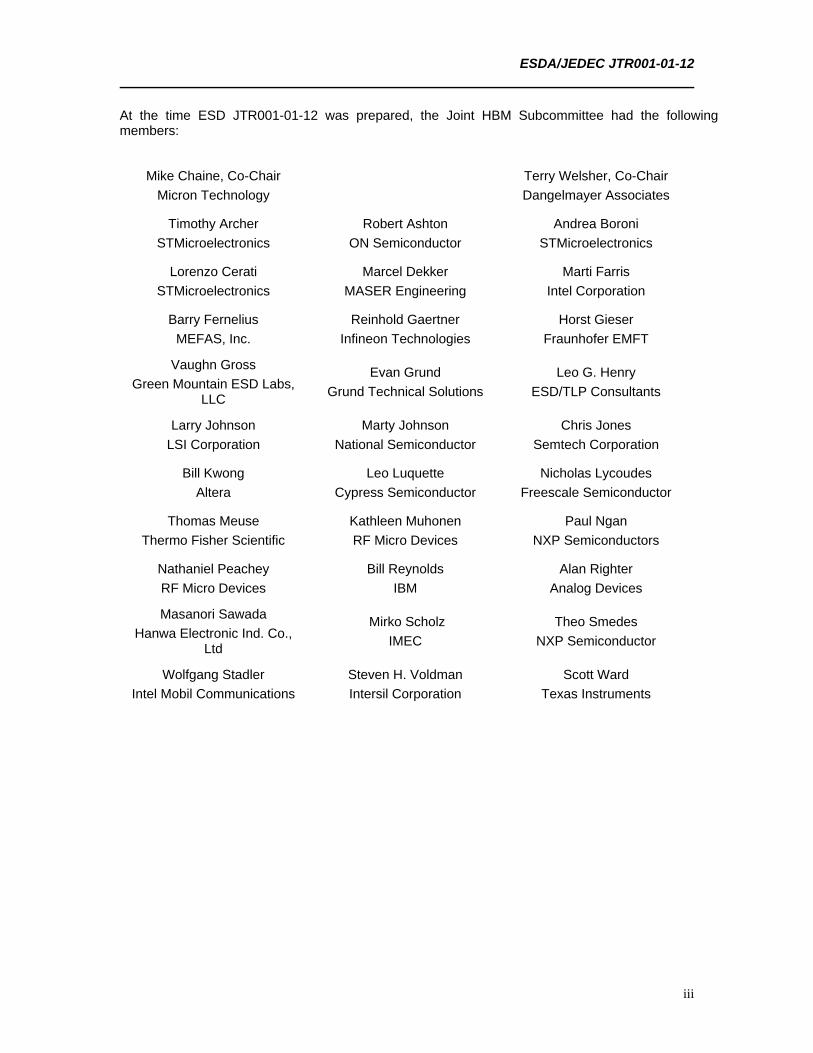
At the time ESD JTR001-01-12 was prepared, the Joint HBM Subcommittee had the following members:
Mike Chaine, Co-Chair
Micron Technology
Terry Welsher, Co-Chair
Dangelmayer Associates
Timothy Archer
STMicroelectronics
Robert Ashton
ON Semiconductor
Andrea Boroni
STMicroelectronics
Lorenzo Cerati
STMicroelectronics
Marcel Dekker
MASER Engineering
Marti Farris
Intel Corporation
Barry Fernelius
MEFAS, Inc.
Reinhold Gaertner
Infineon Technologies
Horst Gieser
Fraunhofer EMFT
Vaughn Gross
Green Mountain ESD Labs, LLC
Evan Grund
Grund Technical Solutions
Leo G. Henry
ESD/TLP Consultants
Larry Johnson
LSI Corporation
Marty Johnson
National Semiconductor
Chris Jones
Semtech Corporation
Bill Kwong
Altera
Leo Luquette
Cypress Semiconductor
Nicholas Lycoudes
Freescale Semiconductor
Thomas Meuse
Thermo Fisher Scientific
Kathleen Muhonen
RF Micro Devices
Paul Ngan
NXP Semiconductors
Nathaniel Peachey
RF Micro Devices
Bill Reynolds
IBM
Alan Righter
Analog Devices
Masanori Sawada
Hanwa Electronic Ind. Co., Ltd
Mirko Scholz
IMEC
Theo Smedes
NXP Semiconductor
Wolfgang Stadler
Intel Mobil Communications
Steven H. Voldman
Intersil Corporation
Scott Ward
Texas Instruments
ESDA/JEDEC JTR001-01-12
iv
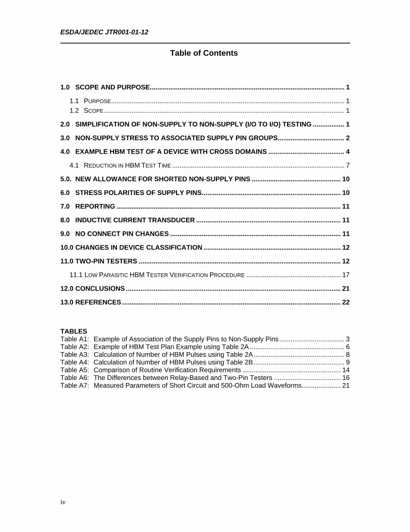
Table of Contents
1.0 SCOPE AND PURPOSE ......................................................................................................... 1
1.1 PURPOSE .............................................................................................................................. 1
1.2 SCOPE .................................................................................................................................. 1
2.0 SIMPLIFICATION OF NON-SUPPLY TO NON-SUPPLY (I/O TO I/O) TESTING ................. 1
3.0 NON-SUPPLY STRESS TO ASSOCIATED SUPPLY PIN GROUPS .................................... 2
4.0 EXAMPLE HBM TEST OF A DEVICE WITH CROSS DOMAINS ......................................... 4
4.1 REDUCTION IN HBM TEST TIME ............................................................................................. 7
5.0. NEW ALLOWANCE FOR SHORTED NON-SUPPLY PINS ................................................ 10
6.0 STRESS POLARITIES OF SUPPLY PINS ........................................................................... 10
7.0 REPORTING ......................................................................................................................... 11
8.0 INDUCTIVE CURRENT TRANSDUCER .............................................................................. 11
9.0 NO CONNECT PIN CHANGES ............................................................................................ 11
10.0 CHANGES IN DEVICE CLASSIFICATION .......................................................................... 12
11.0 TWO-PIN TESTERS ............................................................................................................. 12
11.1 LOW PARASITIC HBM TESTER VERIFICATION PROCEDURE ................................................... 17
12.0 CONCLUSIONS .................................................................................................................... 21
13.0 REFERENCES ...................................................................................................................... 22
TABLES Table A1: Example of Association of the Supply Pins to Non-Supply Pins ................................... 3 Table A2: Example of HBM Test Plan Example using Table 2A ................................................... 6 Table A3: Calculation of Number of HBM Pulses using Table 2A ................................................. 8 Table A4: Calculation of Number of HBM Pulses using Table 2B ................................................. 9 Table A5: Comparison of Routine Verification Requirements ..................................................... 14 Table A6: The Differences between Relay-Based and Two-Pin Testers .................................... 16 Table A7: Measured Parameters of Short Circuit and 500-Ohm Load Waveforms ..................... 21
ESDA/JEDEC JTR001-01-12
v
FIGURES Figure 1: Illustrates the Ideas of Group, Multiple Power Supplies and Coupled Non-Supply Pin Pairs ........................................................................................................................ 5 Figure 2: Pin out of 8 Pin Example Product .................................................................................. 7 Figure 3: Example of Waveform Measurement Setup with Evaluation Load at the DUT Location ....................................................................................................................... 15 Figure 4: Illustrates the Tester Parasitic Affects on the Terminal A and B Discharge HBM Currents .............................................................................................................. 17 Figure 5: Shorting Test Device for Low Parasitic Tester Evaluation .......................................... 18 Figure 6: HBM Tester being Evaluated for Low Parasitics ......................................................... 19 Figure 7: 40 Pin DIP Shorting Test Device with the Current Probe Connected between the Unconnected Pin 1 and Group Connected Pin 40 ................................................ 19 Figure 8: Applying the Negative Pulse (Terminal A) to Pin 40 with Pin 1 Grounded (Terminal B) ................................................................................................................. 20 Figure 9: Plot of Waveforms from a Low Parasitic Tester .......................................................... 21 Figure 10: Plot of 500-Ohm Load Waveforms from a Low Parasitic Tester ................................. 21
ESDA/JEDEC Joint Technical Report ESDA/JEDEC JTR001-01-12
1
ESDA/JEDEC Joint Technical Report User Guide of ANSI/ESDA/JEDEC JS-001 Human Body Model Testing of Integrated Circuits
1.0 PURPOSE AND SCOPE
1.1 Purpose
The information and procedures explained in this technical report are intended to help those familiar with traditional HBM testing use the new options that were introduced in JS-001-2011. JS-001-2011 has since been superseded by JS-001-2012 but all of the changes discussed in this guide were retained in the 2012 version.
1.2 Scope
This report describes the technical changes made in ANSI/ESDA/JEDEC JS-001-2011 and explains how to use those changes to apply HBM (Human Body Model) tests to IC components.
2.0 SIMPLIFICATION OF NON-SUPPLY TO NON-SUPPLY (I/O TO I/O) TESTING
(JS-001-2011 SECTION 6.3.3.1)
In the JS-001-2010 HBM standard, non-supply pins to non-supply pins [I/O to I/O] testing was accomplished by applying HBM pulses (positive and negative) to each non-supply pin (Terminal A) with all other non-supply pins tied together to ground (Terminal B). Table 2 defined the required stress pin combinations and this specific pin combination was defined as Pin Combination Set N+1.
This one-to-many pin combination method was introduced in the early days of HBM testing as a convenience for what was then considered to be high pin count devices (> 40 pins). As the number of pins on an IC component has increased from a few tens of pins to hundreds and now thousands of pins, this specific pin combination test has not changed. In Japan, the non-supply to non-supply pin test was removed from JEITA HBM test method (EIAJ ESD-4701/304-2 in 2001).
This one-to-many pin combination method has multiple issues:
1. This pin combination only represents a small fraction of the possible non-supply to non-supply pin combinations.
2. This procedure does not represent a real ESD pin combination situation, as simultaneous grounding of all non-supply pins is not realistic.
3. The procedure does not address the potentially real non-supply to non-supply two-pin stress combinations.
4. Almost all non-supply to non-supply pin combination failures can generally be repeated in the non-supply pin to supply pin combination test.
As a result, the new HBM Standard JS-001-2011 has given the user the option of doing the following:
A. Apply the non-supply to non-supply pin test to a set of pins called coupled non-supply pin pairs as defined in Section 3.0 and JS-001-2011 Table 2A. This test is a set of specific pin-to-pin tests.
Or
B. Continue to test the non-supply to non-supply pin defined in JS-001-2011 Table 2B, which is the same as JS-001-2010 Table 2. This test stresses each non-supply pin to the combined set of all other non-supply pins.
This change allows the user to set-up their HBM test programs so that one pin of the coupled non-supply pin pair is stressed on Terminal A and the other pin is grounded on Terminal B (Table 2A). Testing these coupled non-supply pin pair combinations is considered to be more vulnerable since they fail more frequently during the traditional non-supply to non-supply pin combinations.
ESDA/JEDEC JTR001-01-12
2
Coupled non-supply pins include differential pairs and other special non-supply pin pairs. Examples of interface pins with differential pairs, which often connect to cables or ports, include USB and HDMI connectors.
For example, consider an integrated circuit with two USB interface pins and a HDMI interface pin group. Each USB pin pair is a single differential pair with pins D+ and D-. According to the new standard, the D+ and D- lines are the only pin pairs that need to be stressed with respect to each other. The signal pins in the first USB port do not need to be stressed to the other signal pin pairs in the second USB port.
Most HDMI pin groups include three high speed differential signal pin pairs and a lower speed differential clock pin pair. The + and – pins within each of the three high speed data lines and the clock pin pair only need to be stressed with respect to each other. No stress is required between the different high speed pin pair groups or with respect to the clock pin pairs.
The HBM test engineer needs to work closely with their engineering support team to correctly identify all coupled non-supply pin pairs. Engineering judgment may be required to determine if such a pin-pair exists on any given IC component. Pin names can be a guide to identify coupled non-supply pin pairs. Examples of names used with coupled non-supply pin pairs are:
USB data pins, such as:
o D+ and D-
o DP and DM
PCI pins, such as:
o TxP and TxN
o RxP and RxN
o DMI_TXN and DMI_TXP
o DMI_RXN and DMI_RXP
A more extensive list of examples of differential pairs is listed in Annex D of the 2011 standard.
Since most non-supply pins do not fit the definition for coupled non-supply pin pairs, significant amount of ESD test time can be saved by eliminating this pin combination from the test program. Since each non-supply pin will be stressed to power and ground, the ESD robustness of every non-supply pin will be fully evaluated.
3.0 NON-SUPPLY STRESS TO ASSOCIATED SUPPLY PIN GROUPS
(JS-001-2011 SECTION 6.5.1.1)
According to HBM Standard JS-001-2010, when an IC component with a large number of power supply groups is HBM tested, the non-supply pins are stressed to each supply and will experience a high number of repetitive stress pulses. As a result, the same pin is stressed multiple times depending on how many independent power supplies are used by the IC component.
The high number of repetitive stresses on the same pin results in several unwanted side effects. This includes the following:
1. Internal wear out failures occurring with lower HBM stress voltages.
2. Premature and low voltage failure of the pins primary ESD protection circuits.
3. Excessively long HBM test times.
The new HBM Standard, JS-001-2011, addresses these issues by associating each non-supply pin with one or more supply pin groups. Section 6.5.1.1 and the Annex C introduce this new method of HBM stressing non-supply pins (input, output and I/O pins) to their local or primary power supply group or groups. In JS-001-2011 Definition Section 3.0, an associated non-supply pin is defined as the supply pin group that directly provides current to the circuits used by those non-supply pins. Sometimes the current is used by the I/O output drivers or sometimes it is used as a voltage level of an input receiver circuit. The key concept is that a direct relationship exists between the pin’s electrical circuits and its power supply pin group or groups.
ESDA/JEDEC JTR001-01-12
3
In addition in part 2 of the definition, there may also occur in an indirect relationship between the non-supply pin and another unrelated supply through a parasitic path. A different type of association between the pad’s active circuits and some other power supply circuitry may occur, for example, a nearby VCC Nwell guardring or some other parasitic device powered by a different supply group.
If an IC has multiple power supply groups, specific non-supply pins may only draw power from one or two of the power supply pin groups. If this is the case, the non-supply pins need to be stressed to both the power supply groups which directly provide power and to any other unrelated supply group that may form a parasitic (bipolar) path. This change will greatly reduce the number of stresses applied to non-supply pin in integrated circuits with multiple power supply pin groups.
The advantage of this new test method becomes important when a set of non-supply pins is HBM stressed. The HBM test plan is simplified as the set of non-supply pins will have to be directly stressed only to their associated power and ground pins and not to all power supply groups. For example, if an IC component has eight different power supply groups, any given I/O pin will have to be directly stressed to perhaps only two power supply pin groups. This change will reduce the total number of ESD pulses to the non-supply pins and will prevent any unintended wear out failure mechanisms.
The new test method also requires that all power and ground supply groups be stressed against one another. This means that power supply group A will be directly stressed to power supply group B and then to power supply pin group C and then to the next supply pin group. Sometimes the package will short together multiple VSS or VDD supply pins, so only one pin out of a group of pins would need to be stressed or grounded.
To perform this simplified test, additional device information is required which will allow the HBM test engineer to correctly assign a pin to specific (power/ground) supply pin group(s). This information is typically provided by the design or product engineering team.
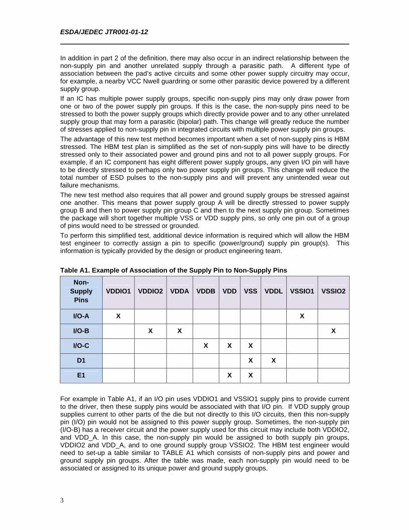
Table A1. Example of Association of the Supply Pin to Non-Supply Pins
Non-Supply
Pins VDDIO1 VDDIO2 VDDA VDDB VDD VSS VDDL VSSIO1 VSSIO2
I/O-A X X
I/O-B X X X
I/O-C X X X
D1 X X
E1 X X
For example in Table A1, if an I/O pin uses VDDIO1 and VSSIO1 supply pins to provide current to the driver, then these supply pins would be associated with that I/O pin. If VDD supply group supplies current to other parts of the die but not directly to this I/O circuits, then this non-supply pin (I/O) pin would not be assigned to this power supply group. Sometimes, the non-supply pin (I/O-B) has a receiver circuit and the power supply used for this circuit may include both VDDIO2, and VDD_A. In this case, the non-supply pin would be assigned to both supply pin groups, VDDIO2 and VDD_A, and to one ground supply group VSSIO2. The HBM test engineer would need to set-up a table similar to TABLE A1 which consists of non-supply pins and power and ground supply pin groups. After the table was made, each non-supply pin would need to be associated or assigned to its unique power and ground supply groups.
ESDA/JEDEC JTR001-01-12
4
After the non-supply pins have been correctly associated with their supply pin groups, the HBM test program may now be written. There are three different test programs that must be developed. They are called the intra-domain test, the inter-domain test, and the non-supply to non-supply test where in the context of this example a domain is equivalent to a Group in Figure 1.
The intra-domain test is a stress combination where each non-supply pin is directly stressed to that supply pin group or groups which have been associated to that pin. For example I/O-A pin is stressed to VDDIO1 and VSSIO1, while IO-B pin is stressed first to VDDIO2, VDDA and then to VSSIO2. Since I/O-A pin is not associated with the other supply pins, these pin combinations are not used in the HBM stress program.
The inter-domain test (matrix test) stresses all power supplies and grounds against each other. For example, the HBM test would stress VDDIO1 to VDDIO2 pins, VDDIO1 to VDDIO3 pins, VDDIO1 to VDDA pins and again separately to the other supply pins.
The non-supply to non-supply test may use one of two different methods. The first method uses the 2010 Standard version where each non-supply pin is stressed to all other non-supply pin that are combined and grounded. The second method reduces the non-supply pins into a much smaller group of pins called the coupled non-supply pin pairs. This much smaller set of pins is stressed in a two pin pair combination test.
To make the results easier to interpret, the stress for all three sections can be performed on a different set of IC components or devices.
4.0 EXAMPLE HBM TEST OF A DEVICE WITH CROSS DOMAINS
A simple example will help introduce how to apply the new changes introduced in the 2011 HBM standard. The ESD test group is given a new IC component which has 16 pins (Figure 1) with four different power domains and three different ground domains (a total of seven supply domains). When the parts are submitted for ESD testing, the engineering group is now required to provide additional information about the pins on this new IC component. The ESD test group has written up new requirements that must be provided by the engineering team when they submit the parts for HBM testing. The HBM test method flow chart shown in JS-001-2011 Annex A was used by the ESD group to collect the following information:
New Required HBM Test Information:
1. List all independent power and ground pins.
2. List all power pins and ground pins that are shorted together in the package.
3. For each non-supply pin assign or associate the power and ground group(s) that provides current to the electrical circuits that directly connect to that pin.
4. List all coupled non-supply pin pairs.
5. List all pins that are no-connects (NC).
ESDA/JEDEC JTR001-01-12
5
Figure 1: Illustrates the Ideas of Group, Multiple Power Supplies and Coupled Non-Supply Pin Pairs
The engineering team had access to this new information and filled out the form as follows:
1. VDD1, VDD2A/B, VDD3, VDD4, VSS1, VSS3/4
2. VSS1, VSS2-A and VSS2-B, VSS3/VSS4
3. Supply pins associated to non-supply pins
a) VDD1 (pin 1) I/O-11 (pin 2), I/O-12 (pin 3)
b) VSS1 (pin 4) I/O-11 (pin 2), I/O-12 (pin 3), I-21 (pin 7), O-21 (pin 8), I/O-21 (pin 9), I/O-22 (1 pin 0)
c) VDD2-A (pin 5)/VDD2-B (pin 6) I-21 (pin 7), O-21 (pin 8), I/O-21 (pin 9), I/O-22 (pin 10)
d) VDD4 (pin 15) I/O-41 (pin 16)
e) VSS3/VSS4 (pin 14) I/O-41 (pin 16)
4. Coupled non-supply pin pairs: I/O-11 (pin 12), I/O-12 (pin 3) and I/O-21 (pin 9), I/O-22 (pin 10)
5. None
(Note: VDD3 was not associated with any non-supply pin, so it was not assigned).
The ESD test group takes this information and uses it to develop their HBM test program. They use JS-001-2011 Annex C and carefully categorize each pin on the IC component into non-supply, supply and NC pins. They follow the flow chart in JS-002-2011 Annex A, page 2 and create their independent supply pin groups. The engineering data allows the non-supply pins (I/O or input pins) to be grouped with their associated supply pin groups (VDD and VSS).
ESDA/JEDEC JTR001-01-12
6
Table A2. Example of HBM Test Plan Example using Table 2A
Pin Combination Set Number
Pin(s) Connected to Terminal B
Pin Connected to Terminal A
(Single Pins, tested one at a time)
1 VDD1
(pin 1)
VSS1 (pin 4)*, VSS3/4 (pin 14),
VDD2-A (pin 5), VDD2-B (pin 6), VDD3 (pin 13), VDD4 (pin 15),
I/O-11 (pin 2), I/O-12 (pin 3)
2 VDD2-A
(pin 5)
VDD1 (pin p1), VSS1 (pin 4), VSS3/4 (pin 14), VDD3 (pin 13), VDD4 (pin 15)
I-21 (pin 7), O-21 (pin 8), I/O-21(pin 9), I/O-22 (pin 10)
3 VDD2-B
(pin 6)
VDD1 (pin 1), VSS1 (pin 4), VSS3/4 (pin 14), VDD3 (pin 13), VDD4 (pin 15)
I-21 (pin 7), O-21 (pin 8), I/O-21(pin 9), I/O-22 (pin 10)
4 VDD3
(pin 13)
VDD1 (pin p1), VSS1 (pin p4)*, VSS3/4 (pin 14), VDD2-A (pin 5), VDD2-B (pin 6), VDD4 (pin 15)
(No associated non-supply pins)
5 VDD4
(pin 15)
VDD1 (pin p1), VSS1 (pin p4)*, VSS3/4 (pin p14), VDD2-A (pin 5), VDD2-B (pin 6), VDD3 (pin 13),
I/O-41(pin 16)
6 VSS1
(pin 4)*
VDD1 (pin 1), VSS3/4 (pin 14),
VDD2-A (pin p5), VDD2-B (pin 6), VDD3 (pin 13), VDD4 (pin 15)
I/O-11 (pin 2), I/O-12 (pin 3), I-21 (pin 7), O-21 (pin 8), I/O-21 (pin 9), I/O-22 (pin 10)
7 VSS3/4
(pin 14)
VDD1 (pin 1), VSS1 (pin 4),
VDD2-A (pin 5), VDD2-B (pin 6), VDD3 (pin 13), VDD4 (pin 15)
I/O-41(pin 16)
8
(i.e., N+1)
I/O-11 (pin 2) I/O-12 (pin 3)
I/O-12 (pin 3) I/O-11 (pin 2)
9
(i.e., N+1)
I/O-21 (pin 9) I/O-22 (pin 10)
I/O-22 (pin 10) I/O-21 (pin 9)
ESDA/JEDEC JTR001-01-12
7
The pin categorization step results in following pin groups:
a. Supply pins: VDD1 (pin 1), VSS1 (pin 4), VDD2-A (pin 5), VDD2-B (pin 6), VDD3 (pin 13), VDD4 (pin 15), VSS3/VSS4 (pin 14)
b. Non-Supply Pin Groups:
a. Group 1: I/O-11 pin (2), I/O-12 (pin 3)
c. Group 2: I/O-11 (pin 2), I/O-12 (pin 3), I-21 (pin 7), O21 (pin 8), I/O-21 (pin 9), I/O-22 (pin 10), I/O-41 (pin 16)
d. Group 3: I-21 (pin 7), O-21 (pin 8), I/O-21 (pin 9), I/O-22 (pin 10)
e. Group 4: I/O-41 (pin 16)
The next step is to develop the HBM test program. Since all of the additional information required in JS-001-2011 Table 2A is available, this procedure can now be used. The new test program is shown in Table A2 *Note: VSS2A and VSS2B are shorted inside the package. Also, VDD2-A and VDD2-B are shorted on the die but are the same supply pins. The non-supply pins 2 and 3 and 9 and 10 are coupled non-supply pin pairs.
4.1 Reduction in HBM Test Time
The changes defined so far can save a significant amount of ESD test time as well as reduce the overstressing of the IC component. The best way to see the advantage of using JS-001-2011 Table 2A instead of Table 2B is to look at another example test case.
Figure 2: Pin out of 8 Pin Example Product
A simple device in Figure 2 is used to illustrate the advantages of reduced pin combinations and is combined with single polarity stress on supply pins. In this example, an 8-pin device has the following pinout:
1. Supply pin group 1: VDD1 (pin 1), VSS1 (pin 2)
2. Supply pin group 2: VDD2 (pin 8), VSS2 (pin 7)
3. Coupled non-supply pin pair: I/O1-1 (pin 3) and I/O1-2 (pin 4)
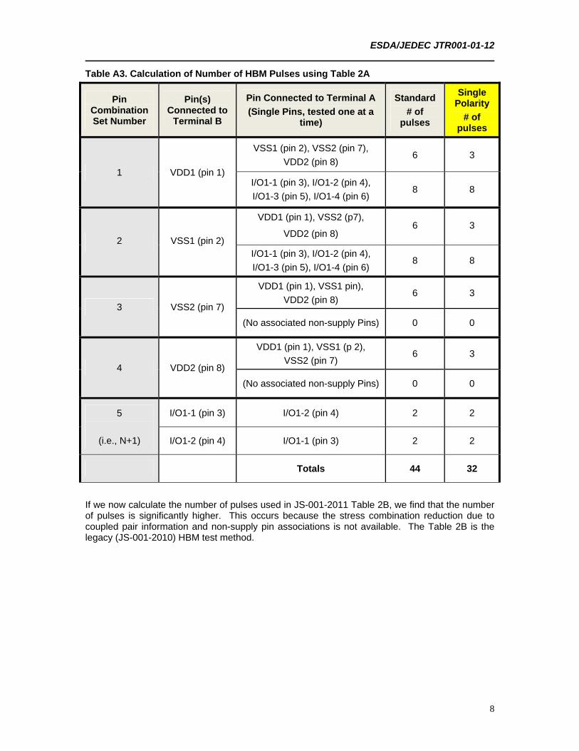
When the device information includes which non-supply pin is associated with which supply pin groups, stressing of I/O pins can be limited to their associated supplies. For the non-supply to non-supply pin test only the two coupled non-supply pin pairs are stressed against each other. The optional Single Polarity supply to supply tests are shown in the last column. Using Table 2A in JS-001-2011 standard and calculate the number of pulses we obtain the results shown in bottom of Table A3.
VDD1 1 8 VDD2VSS1 2 7 VSS2I/O1-1 3 6 I/O1-4I/O1-2 4 5 I/O1-3
Coupled
pin pair
ESDA/JEDEC JTR001-01-12
8
Table A3. Calculation of Number of HBM Pulses using Table 2A
Pin Combination Set Number
Pin(s) Connected to
Terminal B
Pin Connected to Terminal A
(Single Pins, tested one at a time)
Standard
# of pulses
Single Polarity
# of pulses
1 VDD1 (pin 1)
VSS1 (pin 2), VSS2 (pin 7),
VDD2 (pin 8) 6 3
I/O1-1 (pin 3), I/O1-2 (pin 4),
I/O1-3 (pin 5), I/O1-4 (pin 6) 8 8
2 VSS1 (pin 2)
VDD1 (pin 1), VSS2 (p7),
VDD2 (pin 8) 6 3
I/O1-1 (pin 3), I/O1-2 (pin 4),
I/O1-3 (pin 5), I/O1-4 (pin 6) 8 8
3 VSS2 (pin 7)
VDD1 (pin 1), VSS1 pin),
VDD2 (pin 8) 6 3
(No associated non-supply Pins) 0 0
4 VDD2 (pin 8)
VDD1 (pin 1), VSS1 (p 2),
VSS2 (pin 7) 6 3
(No associated non-supply Pins) 0 0
5
(i.e., N+1)
I/O1-1 (pin 3) I/O1-2 (pin 4) 2 2
I/O1-2 (pin 4) I/O1-1 (pin 3) 2 2
Totals 44 32
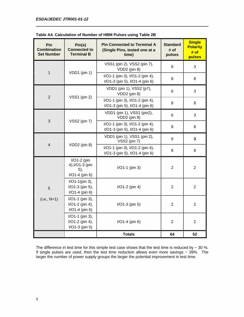
If we now calculate the number of pulses used in JS-001-2011 Table 2B, we find that the number of pulses is significantly higher. This occurs because the stress combination reduction due to coupled pair information and non-supply pin associations is not available. The Table 2B is the legacy (JS-001-2010) HBM test method.
ESDA/JEDEC JTR001-01-12
9
Table A4. Calculation of Number of HBM Pulses using Table 2B
Pin Combination Set Number
Pin(s) Connected to
Terminal B
Pin Connected to Terminal A (Single Pins, tested one at a
time)
Standard # of
pulses
Single Polarity
# of pulses
1 VDD1 (pin 1)
VSS1 (pin 2), VSS2 (pin 7), VDD2 (pin 8)
6 3
I/O1-1 (pin 3), I/O1-2 (pin 4), I/O1-3 (pin 5), I/O1-4 (pin 6)
8 8
2 VSS1 (pin 2)
VDD1 (pin 1), VSS2 (p7), VDD2 (pin 8)
6 3
I/O1-1 (pin 3), I/O1-2 (pin 4), I/O1-3 (pin 5), I/O1-4 (pin 6)
8 8
3 VSS2 (pin 7)
VDD1 (pin 1), VSS1 (pin2), VDD2 (pin 8)
6 3
I/O1-1 (pin 3), I/O1-2 (pin 4), I/O1-3 (pin 5), I/O1-4 (pin 6)
8 8
4 VDD2 (pin 8)
VDD1 (pin 1), VSS1 (pin 2), VSS2 (pin 7)
6 3
I/O1-1 (pin 3), I/O1-2 (pin 4), I/O1-3 (pin 5), I/O1-4 (pin 6)
8 8
5
(i.e., N+1)
I/O1-2 (pin 4),I/O1-3 (pin
5), I/O1-4 (pin 6)
I/O1-1 (pin 3) 2 2
I/O1-1(pin 3), I/O1-3 (pin 5), I/O1-4 (pin 6)
I/O1-2 (pin 4) 2 2
I/O1-1 (pin 3), I/O1-2 (pin 4), I/O1-4 (pin 6)
I/O1-3 (pin 5) 2 2
I/O1-1 (pin 3), I/O1-2 (pin 4), I/O1-3 (pin 5)
I/O1-4 (pin 6) 2 2
Totals 64 52
The difference in test time for this simple test case shows that the test time is reduced by ~ 30 %. If single pulses are used, then the test time reduction allows even more savings ~ 39%. The larger the number of power supply groups the larger the potential improvement in test time.
ESDA/JEDEC JTR001-01-12
10
5.0 NEW ALLOWANCE FOR SHORTED NON-SUPPLY PINS
(JS-001-2011 SECTION 6.4.2)
The requirement to remove non-supply pins that are shorted to the pin under test during the non-supply to non-supply stress combination has been in place for several years. This requirement is necessary to determine the pin-to-pin robustness of shorted non-supply pins, but it can be difficult to generate automated stress test plans to facilitate this requirement.
For non-supply pin groups that are shorted via a package plane or bonded to a common bond pad, a single non-supply pin in the group may be selected to represent the group. The other shorted non-supply pins in the group may be removed from all stress combinations and left unselected during stress.
For example, if an IC component has 8 voltage reference pins (i.e., non-supply pins) shorted by a package substrate, then one pin may be arbitrarily selected to represent the group. This pin would be stressed like all other non-supply pins. The other 7 voltage reference pins would be left “floating” during the all other HBM tests.
If a relay matrix HBM simulator is used and the shorted pins are placed in the socket, then the pins do not truly float. Instead they remain connected to open relays and are parasitically connected to tester. The only way to truly float these pins is to remove their pogo pins or build a special test fixture board which does not connect these pins to the tester channels.
6.0 STRESS POLARITIES OF SUPPLY PINS
(JS-001-2011 Section 6.5.1.2)
In Section 6.5.1.2 the new standard allows the user to apply a single polarity stress when pins of a supply pin group are stressed to a different supply pin group. Either positive or negative polarity may be used. This allowance is limited to supply pins as non-supply pins are still required to be stressed using both positive and negative polarity.
As supply pins are stressed on both Terminal A and on Terminal B, HBM current will flow in both directions between the pins, so that ESD weaknesses should be detected even though only one polarity of stress is performed. This allowance also lowers the risk of cumulative stress on supply pins as HBM pulses applied directly to these pins will be significantly reduced.
Research papers [3], [6] have shown that the parasitics of some HBM testers, arising from tester loading of pins that should be floating, can make a difference. These parasitics are recognized in sections 6.5.1.2 and 6.5.1.3 of JS-001-2011, with allowances that can be used when such parasitics produce false failures.
A low parasitic tester (Section 11.0) will have nearly identical peak currents and rise times on Terminal A and Terminal B, when testing devices. Some testers can be shown not to have significant parasitics and produce stress currents in both directions, meeting the waveform requirements in Section 5.2.3 of JS-001-2011, on a DUT that interconnects tester channels with either orientation of Terminals A or B. The DUT used for this test needs to interconnect tester channels to verify that connection to “floating” tester channels does not affect the HBM current waveforms. With low parasitic testers the floating channels do not affect the test, so reversing the Terminals A and B and retesting is redundant when testing a pin pair with both polarities.
Parasitic capacitance in relay based testers is known to adversely affect test results for devices with multi-pin supply pin groups [6]. The adverse effect is usually more pronounced for one stress polarity than for the other. For most devices with p-type substrates the adverse effects are less for positive stress [3]. Other technologies may exist where the negative stress is less affected by parasitic capacitance. This allowance allows the stress polarity to be chosen such that tester parasitic effects are minimized.
ESDA/JEDEC JTR001-01-12
11
7.0 REPORTING
(JS-001-2011 SECTION 6.5)
A new requirement has been added to Section 6.5 titled “Pin Combinations”. In all previous standards, the user was required to report the HBM test results and the classification level the IC component achieved. In the 2011 version, the user is now required to keep a record of the pin combination tests used during the tests. This new requirement is important if the user applies any of the new pin combination options available.
If Table 2A (Required Pin Combinations Sets) is used, then the non-supply pins must be associated with their corresponding supply pins. This information must be recorded and is similar to Table A1 shown previously in Section 3.0 of this User Guide. This list also identifies those independent supply groups that will be stressed separately during the supply to supply pin group combination.
In addition, each non-supply pin that meets the coupled non-supply pin pair definition will also need to be identified and listed. The other pins that do not fit into this group will not be stressed during the N+1 pin combination tests.
If JS-001-2011 Table 2B (Legacy Pin Combinations Sets equivalent to Table 2 of ANSI/ESDA/JEDEC JS-001-2010) is used, then this information must be reported in the classification report.
Sometimes, Tables 2A and 2B can be used in combination. The pin combinations from Table 2A and Table 2B would have to be clearly identified. For example, if the additional information required to associate the power supply pin groups to the non-supply pins is not available, but the coupled non-supply pin pair is available, then the testing of all non-supply pins to all power supply groups defined in Table 2B would be documented. In addition, the testing of the coupled non-supply pin pair would also be recorded and referenced from Table 2A. The reporting of this information will document how the ESD test programs were developed and may be used again for additional new designs.
8.0 INDUCTIVE CURRENT TRANSDUCER
(JS-001-2011 SECTION 4.1.2)
The 2011 version of the HBM standard encourages the use of probes like the Tektronix CT2 current probe, as the CT2 offers a more accurate representation of the short-circuit waveform on the scale of 150 nanoseconds and beyond, owing to its superior low-frequency performance [2]. If the decay time is less than 130 nanoseconds when measured with a CT1 probe, the CT2 probe may give a more accurate measurement of the decay time. This is particularly important at higher voltages (e.g., 4kV and above), because of the heavy dependence on current of the low frequency cutoff of the current probes.
9.0. NO-CONNECT PIN CHANGES
The basic requirement for no-connect pins is that they must not be stressed and must be left floating at all times, if verified as not having a connection to the die. However, there are cases where pins defined as no connects in the data sheet, such as thermal panels, can have a connection to the die. If such pins exist, then the pin is classified as either a supply pin (if pin is found to have a metallic connection to a supply pin) or a non-supply pin (if pin is found to have a connection to any other electrical node on the die). The sections dealing with no-connect pins are quoted below.

ESDA/JEDEC JTR001-01-12
12
JS-001-2010 No-Connect Pins Section:
6.4 No-Connect Pins
Pins labeled as no-connect pins but found to have an electrical connection to the die shall be tested as non-supply pins. Verified no-connect pins must not be stressed and must be left floating at all times.
JS-001-2011 No-Connect Pins Section:
6.3.1 No-Connect Pins
Verified no-connect pins must not be stressed and must be left floating at all times.
There are some pins which are labeled as no connect, such as thermal panels, which are actually connected to the die and should be classified either as a supply pin or non-supply pin, as outlined below.
Pins labeled as no connect but found to have an electrical connection to the die shall be:
Classified as a supply pin, if metallically connected to a supply pin.
Classified as a non-supply pin, if not metallically connected to a supply pin.
10.0 CHANGES IN DEVICE CLASSIFICATIONS
(JS-001-2011 Section 8.0)
The HBM classifications have been modified to take into account the trend towards lower device thresholds. The Class 0 range is now split into two sub-ranges 0A (< 125 volts) and 0B (125 to < 250 volts). All other classes remain the same. These classifications are chosen to be consistent with the recommended test levels. When testing at lower levels is deemed reliable and repeatable, the 0A sub-range will be subdivided further. The determination of what controls are needed to guarantee safe handling of devices is not in the scope of this document.
11.0 TWO-PIN TESTERS
The interactions between ICs and testers have increased due to continued technology scaling, the decrease in power supply voltages, the trend to higher pin count device and the complexity of high pin count HBM test equipment. The IC-tester interactions can produce false device failures causing improper ESD sensitivity classifications.
Today’s large low voltage devices have many power pins connected in parallel to conduct high supply currents. When these devices are inserted into a relay matrix tester, matrix channels are connected together by the device under test (DUT) and the parasitic capacitances of tester wiring and relays provide a load to the pulse that is in parallel with the DUT. When the device interconnects the HBM tester channels, the tester cannot deliver the standard HBM stress to a single pin in the group. Such DUT- tester interactions have been shown to change the stress pulses and can produce either less or more stress than intended by the HBM standard waveforms. A tester design that eliminates the interconnection of tester channels and provides the same stress to all DUT pins can provide a more reliable test. Delivering HBM stress pulses between pairs of pins rather than in groups of pins provides a test with less variability and therefore can improve test repeatability and reproducibility. The new revision of the HBM Standard now allows the use of two pin testers to stress any IC component.
HBM testing of two pin in the DUT at a time is not a new concept. The most “idealized” HBM test would be to stress all two-pin combinations. JS-001-2011 recommends to “test all pairs” pin combinations for all devices with ten pins or less. However, this approach is not practical for
ESDA/JEDEC JTR001-01-12
13
large pin count parts. Many changes have been made in JS-001-2011 to reduce the pin combinations, and these changes make testing using a two-pin simulator more practical. There are several types of devices that can benefit from testing with two-pin testers, including:
1. Low pin count devices
2. Devices that show questionable results when tested on a relay-based tester, possibly due to DUT to tester parasitic interactions
3. Bare die or wafer level devices, where test fixtures or sockets are not available or appropriate
4. Devices with more pins than available relay-based testers have channels, although their test time will be quite long
A two-pin HBM simulator tests exclusively in pin pair combinations. This can be coupled with non-socketed testing where probes connect only to the two device pins (or balls, lands, bumps or pads) being tested. Connecting only to the pins being tested has the advantage that all pins that should be floating are truly floating and not loaded by tester wiring with unwanted parasitics.
Without a relay matrix and multiple pulse sources, the HBM simulator is simplified to insure that the specified HBM stress pulse is uniformly delivered to all pairs of pins, balls, lands, or pads of any device. However, the test time is significantly increased for two-pin testing, as more two-pin combinations are stressed when testing to all supply pins, instead of groups of supply pins organized (by relay matrices). Two-pin HBM testing sacrifices testing throughput and speed to gain testing accuracy. The simplified required pin combinations in the 2011 standard Table 2A reduce test times on all simulators, and this is especially important for two-pin testers.
JS-001-2011 enables two-pin testing by making these changes to the previous HBM standard:
1. All one-to-many pin combinations described in the HBM standard can be divided into one-to-one combinations so that all devices can be stressed with two-pin combinations. All pin combinations with Terminal B supply pin groups larger than a single pin are subdivided to a set of individual pins, and each Terminal A pin is tested with respect to every pin of the Terminal B group individually.
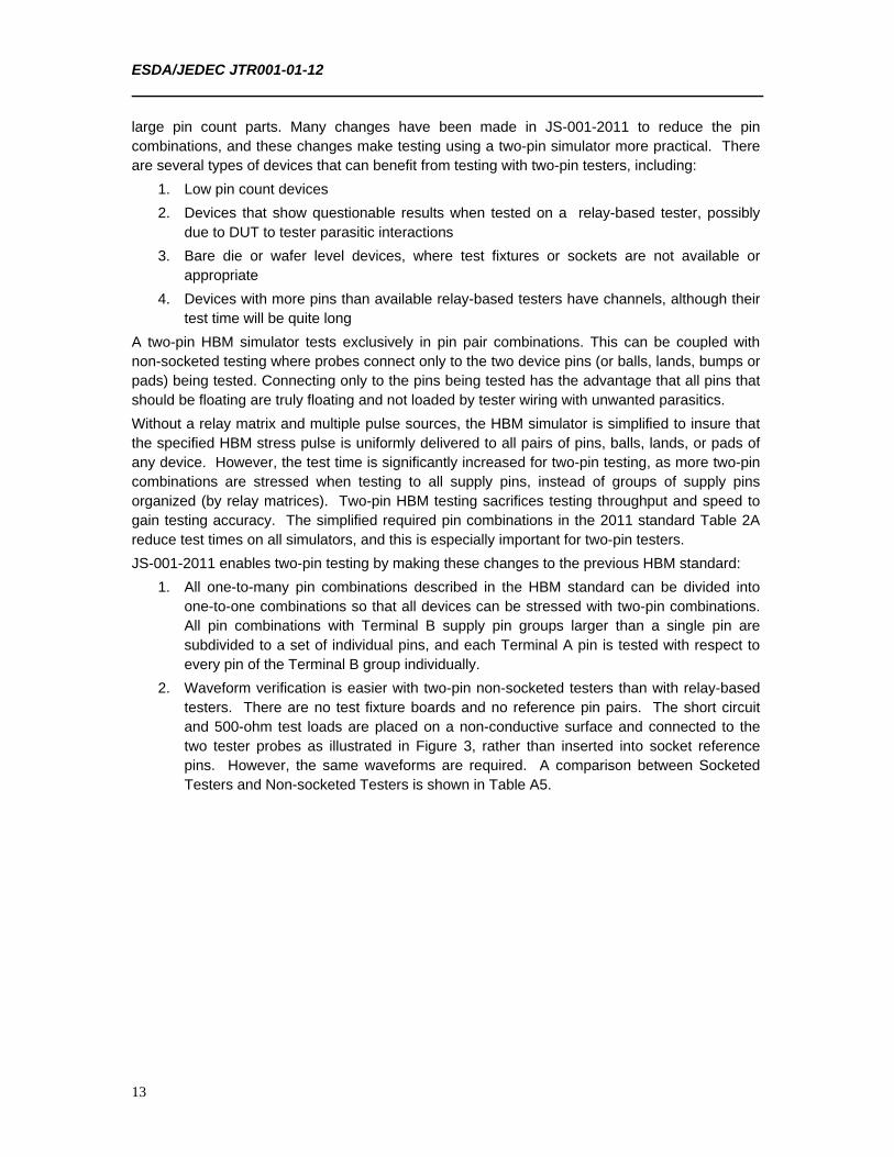
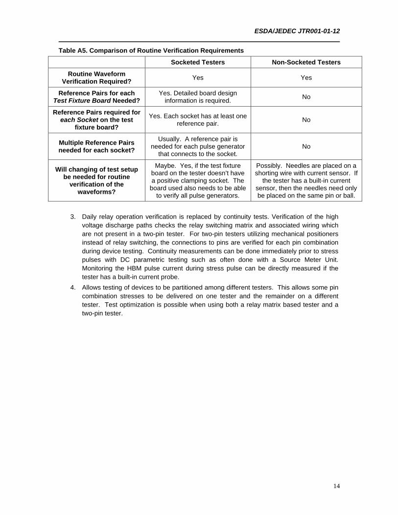
2. Waveform verification is easier with two-pin non-socketed testers than with relay-based testers. There are no test fixture boards and no reference pin pairs. The short circuit and 500-ohm test loads are placed on a non-conductive surface and connected to the two tester probes as illustrated in Figure 3, rather than inserted into socket reference pins. However, the same waveforms are required. A comparison between Socketed Testers and Non-socketed Testers is shown in Table A5.
ESDA/JEDEC JTR001-01-12
14
Table A5. Comparison of Routine Verification Requirements
Socketed Testers Non-Socketed Testers
Routine Waveform Verification Required?
Yes Yes
Reference Pairs for each Test Fixture Board Needed?
Yes. Detailed board design information is required.
No
Reference Pairs required for each Socket on the test
fixture board?
Yes. Each socket has at least one reference pair.
No
Multiple Reference Pairs needed for each socket?
Usually. A reference pair is needed for each pulse generator
that connects to the socket. No
Will changing of test setup be needed for routine
verification of the waveforms?
Maybe. Yes, if the test fixture board on the tester doesn’t have a positive clamping socket. The
board used also needs to be able to verify all pulse generators.
Possibly. Needles are placed on a shorting wire with current sensor. If
the tester has a built-in current sensor, then the needles need only be placed on the same pin or ball.
3. Daily relay operation verification is replaced by continuity tests. Verification of the high voltage discharge paths checks the relay switching matrix and associated wiring which are not present in a two-pin tester. For two-pin testers utilizing mechanical positioners instead of relay switching, the connections to pins are verified for each pin combination during device testing. Continuity measurements can be done immediately prior to stress pulses with DC parametric testing such as often done with a Source Meter Unit. Monitoring the HBM pulse current during stress pulse can be directly measured if the tester has a built-in current probe.
4. Allows testing of devices to be partitioned among different testers. This allows some pin combination stresses to be delivered on one tester and the remainder on a different tester. Test optimization is possible when using both a relay matrix based tester and a two-pin tester.
ESDA/JEDEC JTR001-01-12
15
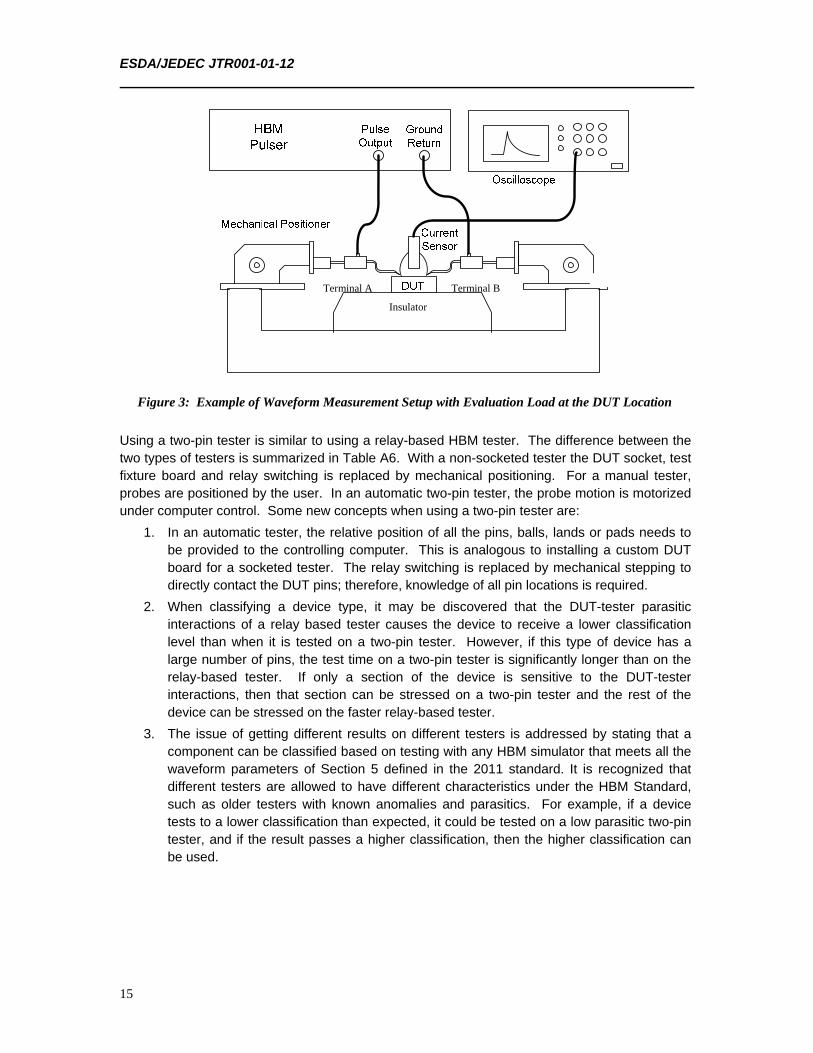
Figure 3: Example of Waveform Measurement Setup with Evaluation Load at the DUT Location
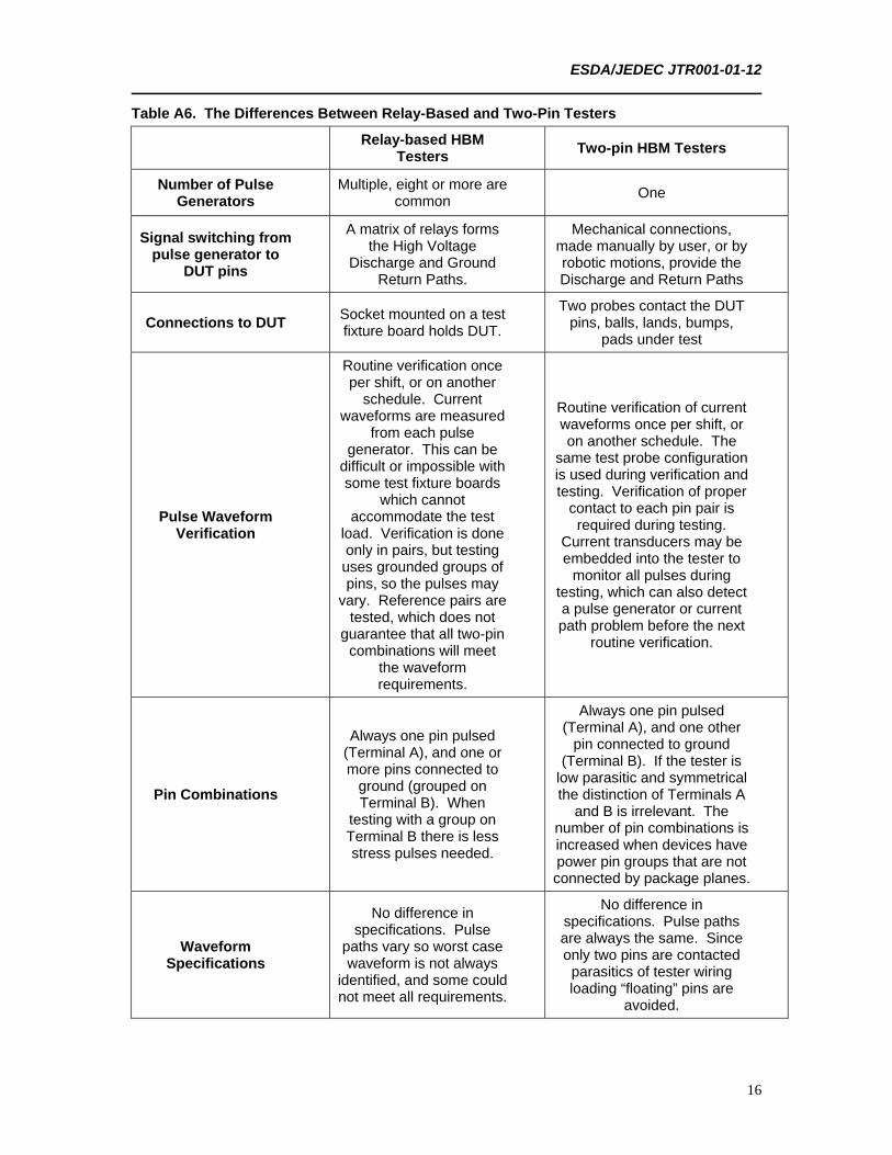
Using a two-pin tester is similar to using a relay-based HBM tester. The difference between the two types of testers is summarized in Table A6. With a non-socketed tester the DUT socket, test fixture board and relay switching is replaced by mechanical positioning. For a manual tester, probes are positioned by the user. In an automatic two-pin tester, the probe motion is motorized under computer control. Some new concepts when using a two-pin tester are:
1. In an automatic tester, the relative position of all the pins, balls, lands or pads needs to be provided to the controlling computer. This is analogous to installing a custom DUT board for a socketed tester. The relay switching is replaced by mechanical stepping to directly contact the DUT pins; therefore, knowledge of all pin locations is required.
2. When classifying a device type, it may be discovered that the DUT-tester parasitic interactions of a relay based tester causes the device to receive a lower classification level than when it is tested on a two-pin tester. However, if this type of device has a large number of pins, the test time on a two-pin tester is significantly longer than on the relay-based tester. If only a section of the device is sensitive to the DUT-tester interactions, then that section can be stressed on a two-pin tester and the rest of the device can be stressed on the faster relay-based tester.
3. The issue of getting different results on different testers is addressed by stating that a component can be classified based on testing with any HBM simulator that meets all the waveform parameters of Section 5 defined in the 2011 standard. It is recognized that different testers are allowed to have different characteristics under the HBM Standard, such as older testers with known anomalies and parasitics. For example, if a device tests to a lower classification than expected, it could be tested on a low parasitic two-pin tester, and if the result passes a higher classification, then the higher classification can be used.
Insulator
Terminal A Terminal B
ESDA/JEDEC JTR001-01-12
16
Table A6. The Differences Between Relay-Based and Two-Pin Testers
Relay-based HBM
Testers Two-pin HBM Testers
Number of Pulse Generators
Multiple, eight or more are common
One
Signal switching from pulse generator to
DUT pins
A matrix of relays forms the High Voltage
Discharge and Ground Return Paths.
Mechanical connections, made manually by user, or by robotic motions, provide the Discharge and Return Paths
Connections to DUT Socket mounted on a test fixture board holds DUT.
Two probes contact the DUT pins, balls, lands, bumps,
pads under test
Pulse Waveform Verification
Routine verification once per shift, or on another
schedule. Current waveforms are measured
from each pulse generator. This can be
difficult or impossible with some test fixture boards
which cannot accommodate the test
load. Verification is done only in pairs, but testing uses grounded groups of pins, so the pulses may
vary. Reference pairs are tested, which does not
guarantee that all two-pin combinations will meet
the waveform requirements.
Routine verification of current waveforms once per shift, or on another schedule. The
same test probe configuration is used during verification and testing. Verification of proper
contact to each pin pair is required during testing.
Current transducers may be embedded into the tester to
monitor all pulses during testing, which can also detect a pulse generator or current path problem before the next
routine verification.
Pin Combinations
Always one pin pulsed (Terminal A), and one or more pins connected to
ground (grouped on Terminal B). When
testing with a group on Terminal B there is less stress pulses needed.
Always one pin pulsed (Terminal A), and one other
pin connected to ground (Terminal B). If the tester is
low parasitic and symmetrical the distinction of Terminals A
and B is irrelevant. The number of pin combinations is increased when devices have power pin groups that are not connected by package planes.
Waveform Specifications
No difference in specifications. Pulse
paths vary so worst case waveform is not always
identified, and some could not meet all requirements.
No difference in specifications. Pulse paths are always the same. Since only two pins are contacted
parasitics of tester wiring loading “floating” pins are
avoided.
ESDA/JEDEC JTR001-01-12
17
11.1 Low Parasitic HBM Tester Verification Procedure
(JS-001-2011 Definitions, Two-pin Tester)
Tester parasitics can vary considerably between different HBM tester designs, but one of the primary issues is the parasitic capacitance on each channel of automated testers. These capacitances can become charged during HBM testing, and can produce ringing from the fast HBM rise times. This is especially true when a high pin count device is inserted into an automated tester socket since the device under test can connect multiple tester channels together, increasing the effective parasitic capacitance. The result is that the current that enters the device from Terminal A (the tester stressing channel) does not match the current leaving the device on Terminal B (the tester grounding channel).
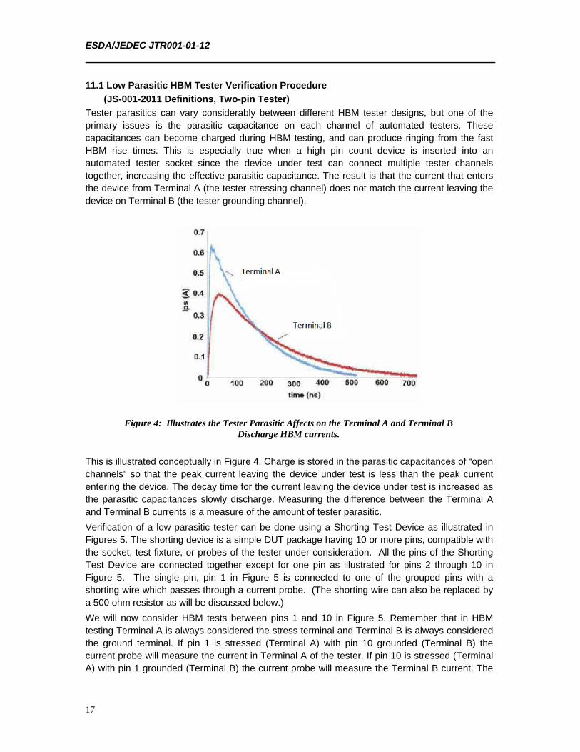
Figure 4: Illustrates the Tester Parasitic Affects on the Terminal A and Terminal B Discharge HBM currents.
This is illustrated conceptually in Figure 4. Charge is stored in the parasitic capacitances of “open channels” so that the peak current leaving the device under test is less than the peak current entering the device. The decay time for the current leaving the device under test is increased as the parasitic capacitances slowly discharge. Measuring the difference between the Terminal A and Terminal B currents is a measure of the amount of tester parasitic.
Verification of a low parasitic tester can be done using a Shorting Test Device as illustrated in Figures 5. The shorting device is a simple DUT package having 10 or more pins, compatible with the socket, test fixture, or probes of the tester under consideration. All the pins of the Shorting Test Device are connected together except for one pin as illustrated for pins 2 through 10 in Figure 5. The single pin, pin 1 in Figure 5 is connected to one of the grouped pins with a shorting wire which passes through a current probe. (The shorting wire can also be replaced by a 500 ohm resistor as will be discussed below.)
We will now consider HBM tests between pins 1 and 10 in Figure 5. Remember that in HBM testing Terminal A is always considered the stress terminal and Terminal B is always considered the ground terminal. If pin 1 is stressed (Terminal A) with pin 10 grounded (Terminal B) the current probe will measure the current in Terminal A of the tester. If pin 10 is stressed (Terminal A) with pin 1 grounded (Terminal B) the current probe will measure the Terminal B current. The
ESDA/JEDEC JTR001-01-12
18
Shorting Test Device therefore allows the measurement of either Terminal A or Terminal B current while a large number of tester channels are tied together at either Terminal A or Terminal B. The comparison of Terminal A current and Terminal B current is further simplified if the sign of the stress is reversed when reversing the stress between pins 1 and 10.
The test procedure is then as follows using a Shorting Test Device similar to that in Figure 5.
1. Use a shorting wire inserted through a current probe to connect pin 1 and pin 10 together
2. Stress pin 1 (Terminal A) at +1 kV with pin 10 grounded (Terminal B) and record the current.
This measures the current in Terminal A.
3. Stress pin 10 (now Terminal A) at -1kV with pin 1 grounded (now Terminal B) and record the current (note the change of polarity).
This measures the current in Terminal B.
4. Replace the shorting wire with a 500 ohm resistor.
5. Stress pin 1 (Terminal A) at +1 kV with pin 10 grounded (Terminal B) and record the current.
This measures the current in Terminal A.
6. Stress pin 10 (Terminal A) at -1kV with pin 1 grounded (Terminal B) and record the current.
This measures the current in Terminal B.
7. If the positive and negative stress waveforms for the short and 500 ohm stress all meet the HBM waveform requirements the tester can be considered a low parasitic tester.
Figure 5: Shorting Test Device for Low Parasitic Tester Evaluation

ESDA/JEDEC JTR001-01-12
19
The low parasitic test procedure is demonstrated on an IMCS/Oryx/Thermo Scientific Model 700 socketed manual HBM tester in Figure 6.
Figure 6: HBM Tester being Evaluated for Low Parasitics
A 40 pin DIP header compatible with the tester socket was prepared by soldering a wire loop connecting pins 2 through 40. A Tektronix CT2 current probe was connected between pins 1 and 40. This Shorting Test Device was inserted into the tester as shown in Figure 7. While as few as 10 pins are adequate for this test, it is recommended to use as large a Shorting Test Device as possible.
Figure 7: 40 Pin DIP Shorting Test Device with the Current Probe Connected between the Unconnected Pin 1 and Group Connected Pin 40
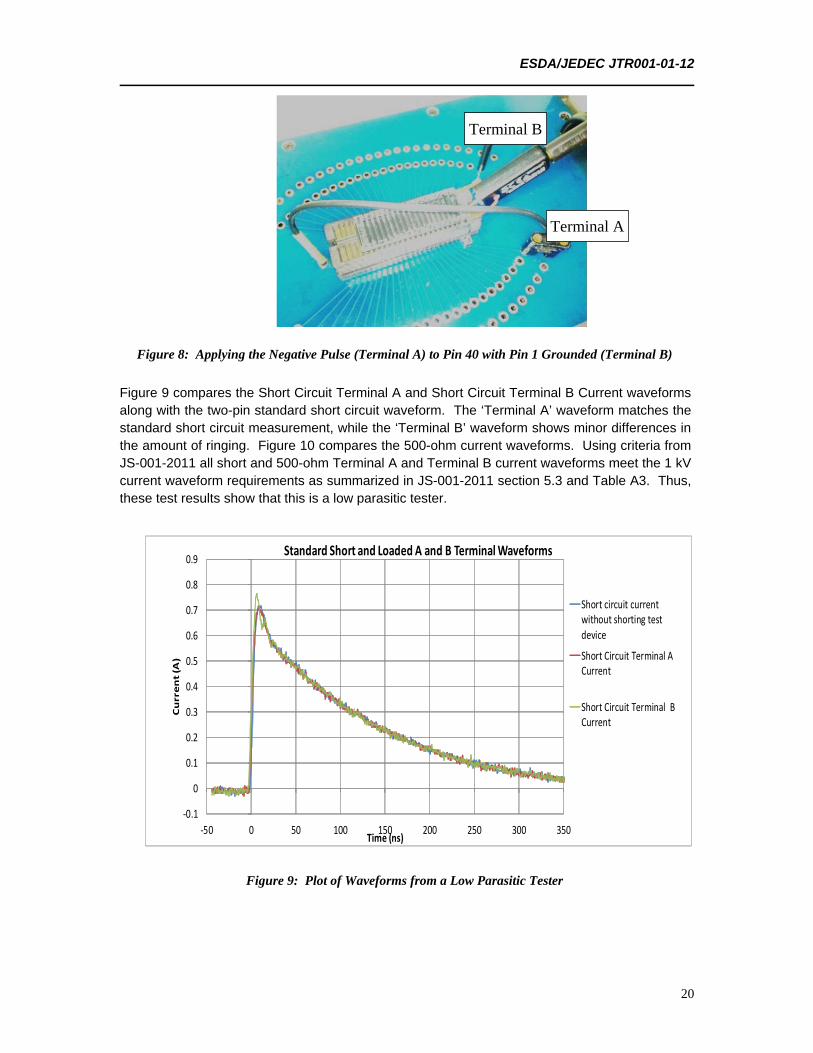
A positive 1 kV pulse was delivered to pin 1 shown as Terminal A while pin 40 is connected to the ground return path shown as Terminal B. The ‘Short Circuit Terminal A Current’ waveform was recorded. The pulse and ground pins were then reversed as shown in Figure 8. The current waveform from negative 1 kV pulse to pin 40 (and by construction also to pins 2 through 39) with pin 1 grounded was recorded as ‘Short Circuit Terminal B Current’.
The short test load was replaced with a 500-ohm resistor and ‘500-ohm Terminal A Current’ and ‘500-ohm Terminal B Current’ waveforms were captured.
Terminal B
ESDA/JEDEC JTR001-01-12
20
Figure 8: Applying the Negative Pulse (Terminal A) to Pin 40 with Pin 1 Grounded (Terminal B)
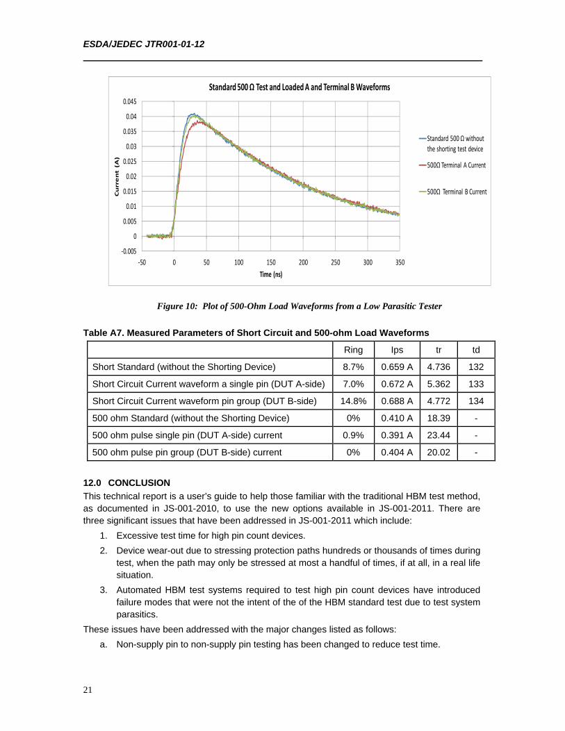
Figure 9 compares the Short Circuit Terminal A and Short Circuit Terminal B Current waveforms along with the two-pin standard short circuit waveform. The ‘Terminal A’ waveform matches the standard short circuit measurement, while the ‘Terminal B’ waveform shows minor differences in the amount of ringing. Figure 10 compares the 500-ohm current waveforms. Using criteria from JS-001-2011 all short and 500-ohm Terminal A and Terminal B current waveforms meet the 1 kV current waveform requirements as summarized in JS-001-2011 section 5.3 and Table A3. Thus, these test results show that this is a low parasitic tester.
‐0.1
0
0.1
0.2
0.3
0.4
0.5
0.6
0.7
0.8
0.9
‐50 0 50 100 150 200 250 300 350
Current (A)
Time (ns)
Standard Short and Loaded A and B Terminal Waveforms
Short circuit currentwithout shorting test
device
Short Circuit Terminal ACurrent
Short Circuit Terminal BCurrent
Figure 9: Plot of Waveforms from a Low Parasitic Tester
Terminal A
Terminal B
ESDA/JEDEC JTR001-01-12
21
‐0.005
0
0.005
0.01
0.015
0.02
0.025
0.03
0.035
0.04
0.045
‐50 0 50 100 150 200 250 300 350
Current (A)
Time (ns)
Standard 500 Ω Test and Loaded A and Terminal B Waveforms
Standard 500 Ω without the shorting test device
500Ω Terminal A Current
500Ω Terminal B Current
Figure 10: Plot of 500-Ohm Load Waveforms from a Low Parasitic Tester
Table A7. Measured Parameters of Short Circuit and 500-ohm Load Waveforms
Ring Ips tr td
Short Standard (without the Shorting Device) 8.7% 0.659 A 4.736 132
Short Circuit Current waveform a single pin (DUT A-side) 7.0% 0.672 A 5.362 133
Short Circuit Current waveform pin group (DUT B-side) 14.8% 0.688 A 4.772 134
500 ohm Standard (without the Shorting Device) 0% 0.410 A 18.39 -
500 ohm pulse single pin (DUT A-side) current 0.9% 0.391 A 23.44 -
500 ohm pulse pin group (DUT B-side) current 0% 0.404 A 20.02 -
12.0 CONCLUSION
This technical report is a user’s guide to help those familiar with the traditional HBM test method, as documented in JS-001-2010, to use the new options available in JS-001-2011. There are three significant issues that have been addressed in JS-001-2011 which include:
1. Excessive test time for high pin count devices.
2. Device wear-out due to stressing protection paths hundreds or thousands of times during test, when the path may only be stressed at most a handful of times, if at all, in a real life situation.
3. Automated HBM test systems required to test high pin count devices have introduced failure modes that were not the intent of the of the HBM standard test due to test system parasitics.
These issues have been addressed with the major changes listed as follows:
a. Non-supply pin to non-supply pin testing has been changed to reduce test time.

ESDA/JEDEC JTR001-01-12
22
b. Non-supply pin testing to all independent power supplies (Cross Domains) has been eliminated to reduce cumulative stress and reduce test time.
c. Supply to Supply testing can be done with a single polarity.
d. Two pin testing is now permitted.
e. The section on Reporting was modified to accommodate the changes in the pin combinations discussed above.
f. Discussion of current probe specifications and the use of CT1 and CT2 current probes with regard to the measurement of the HBM decay time.
g. Change in wording for non-supply pins which are shorted together.
h. Changes to the wording on No Connect Pins.
i. Class 0 has been divided into 2 classes.
13.0 REFERENCES
[1] R. Gaertner; Partitioned HBM Test - A New Method to Perform HBM Tests on Complex Devices; EOS/ESD Symposium 2005
[2] Timothy J. Maloney, “HBM Tester Waveforms, Equivalent Circuits, and Socket Capacitance”, EOS/ESD Symposium Proceedings, 2010, pp. 407-415.
[3] H. Kunz, et al., “The Effect of High Pin-Count ESD Tester Parasitics on Transiently Triggered ESD Clamps”, 2004 EOS/ESD Symposium Proceedings.
[4] Y-Y. Lin, et al., “Problems with I/O to All Other I/Os ESD Stress Test: Two Case Studies”, 2005 EOS/ESD Symposium Proceedings
[5] K. T. Kaschani, et.al., "About the Impact of Anomalous ESD Pulses on the Qualification of Integrated Circuits", Proceedings of 9th ESD Forum of the Interessengemeinschaft ElectroStatic Discharge e.V., Berlin Germany, 2005.
[6] M. Chaine, et al., “HBM Tester Parasitic Effects on High Pin Count Devices with Multiple Power and Ground Pins”, 2006 EOS/ESD Symposium Proceedings.
[7] R. Given, et al., "Study of the Impact of Non-selected I/O Pins during HBM Test using ZapMaster Mk.2", Conformity, September 2007. (http://www.conformity.com/1851)
[8] T. Brodbeck, et al., “Statistical Pin Pair Combinations, A New Proposal for Device Level HBM Tests”, 2008 EOS/ESD Symposium Proceedings
[9] E. Grund, “Two-Pin Human Body Model Testing”, 2009 EOS/ESD Symposium Proceedings.
[10] S. Ward, et al., “Overcoming the Unselected Pin Relay Capacitance HBM Tester Artifact with Two Pin HBM testing”, 2010 EOS/ESD Symposium Proceedings.