Embed Size (px)
Citation preview

VIN
ENA
D1A
D2A
D1B
D2B
ENB
VENA
VENB
ISET
VBATT
TPS7510x
Product
Folder
Sample &Buy
Technical
Documents
Tools &
Software
Support &Community
An IMPORTANT NOTICE at the end of this data sheet addresses availability, warranty, changes, use in safety-critical applications,intellectual property matters and other important disclaimers. PRODUCTION DATA.
TPS75100, TPS75103, TPS75105SBVS080J –SEPTEMBER 2006–REVISED NOVEMBER 2016
TPS7510x Low Dropout, Two-Bank LED Driver With PWM Brightness Control
1
1 Features1• Regulated Output Current with 2% LED-to-LED
Matching• Drives Up to Four LEDs at 25 mA Each in a
Common Cathode Topology• 28-mV Typical Dropout Voltage Extends Usable
Supply Range in Li-Ion Battery Applications• Brightness Control Using PWM Signals• Two 2-LED Banks With Independent Enable and
PWM Brightness Control per Bank• No Internal Switching Signals—Eliminates EMI• Default LED Current Eliminates External
Components– Default Values from 3 mA to 10 mA (in 1-mA
Increments) Available Using Innovative FactoryEEPROM Programming
– Optional External Resistor can be Used forHigh-Accuracy, User-Programmable Current
• Over current and Over temperature Protection• Available in Wafer Chip-Scale Package
or 2.50-mm × 2.50-mm WSON-10
2 Applications• Keypad and Display Backlighting• White and Color LEDs• Cellular Handsets• PDAs and Smartphones
3 DescriptionThe TPS7510x linear low dropout (LDO) matchingLED current source is optimized for low-powerkeypad and navigation pad LED backlightingapplications. The device provides a constant currentto up to four unmatched LEDs organized in two banksof two LEDs each in a common-cathode topology.Without an external resistor, the current sourcedefaults to a factory-programmable, preset currentlevel with ±0.5% accuracy (typical). An optionalexternal resistor can be used to set initial brightnessto user-programmable values with higher accuracy.Brightness can be varied from off to full brightness byinputting a pulse width modulation (PWM) signal oneach enable pin (ENx, where x indicates LED bank Aor B). Each bank has independent enable andbrightness control, but current matching is done to allfour channels concurrently. The input supply range isideally suited for single-cell Li-Ion battery suppliesand the TPS7510x can provide up to 25 mA per LED.
No internal switching signals are used, eliminatingtroublesome electromagnetic interference (EMI). TheTPS7510x is offered in an ultra-small, 9-ball, 0.4-mmball-pitch wafer chip-scale package (WCSP) and a2.50-mm × 2.50-mm, 10-pin WSON package, yieldinga very compact total solution size ideal for mobilehandsets and portable backlighting applications. Thedevice is fully specified over TJ = –40°C to +85°C.
Device Information(1)
PART NUMBER PACKAGE BODY SIZE (NOM)
TPS7510xWSON (10) 2.50 mm × 2.50 mmDSBGA (9) 1.208 mm x 1.208 mm
(1) For all available packages, see the orderable addendum atthe end of the data sheet.
Typical Application Diagram
2
TPS75100, TPS75103, TPS75105SBVS080J –SEPTEMBER 2006–REVISED NOVEMBER 2016 www.ti.com
Product Folder Links: TPS75100 TPS75103 TPS75105
Submit Documentation Feedback Copyright © 2006–2016, Texas Instruments Incorporated
Table of Contents1 Features .................................................................. 12 Applications ........................................................... 13 Description ............................................................. 14 Revision History..................................................... 25 Pin Configuration and Functions ......................... 36 Specifications......................................................... 4
6.1 Absolute Maximum Ratings ...................................... 46.2 ESD Ratings.............................................................. 46.3 Recommended Operating Conditions....................... 46.4 Thermal Information .................................................. 46.5 Electrical Characteristics........................................... 56.6 Typical Characteristics .............................................. 6
7 Detailed Description .............................................. 87.1 Overview ................................................................... 87.2 Functional Block Diagram ......................................... 87.3 Feature Description................................................... 97.4 Device Functional Modes.......................................... 9
8 Application and Implementation ........................ 108.1 Application Information............................................ 108.2 Typical Application .................................................. 12
9 Power Supply Recommendations ...................... 1410 Layout................................................................... 14
10.1 Layout Guidelines ................................................. 1410.2 Layout Example .................................................... 14
11 Device and Documentation Support ................. 1511.1 Device Support...................................................... 1511.2 Documentation Support ........................................ 1511.3 Related Links ........................................................ 1511.4 Receiving Notification of Documentation Updates 1511.5 Community Resources.......................................... 1511.6 Trademarks ........................................................... 1611.7 Electrostatic Discharge Caution............................ 1611.8 Glossary ................................................................ 16
12 Mechanical, Packaging, and OrderableInformation ........................................................... 16
4 Revision HistoryNOTE: Page numbers for previous revisions may differ from page numbers in the current version.
Changes from Revision I (November 2013) to Revision J Page
• Added Device Information table, Typical Application Diagram title to front-page diagram, ESD Ratings table,Thermal Information table, Feature Description section, Device Functional Modes section, Application andImplementation section, Power Supply Recommendations section, Layout section, Device and DocumentationSupport section, and Mechanical, Packaging, and Orderable Information section ............................................................... 1
• Changed SON to WSON throughout document .................................................................................................................... 1• Deleted pin out drawings from Typical Application Diagram figure........................................................................................ 1• Changed I/O status to I from O in D1B row of Pin Functions table ....................................................................................... 3• Deleted Dissipation Ratings table........................................................................................................................................... 4
Changes from Revision H (January 2010) to Revision I Page
• Changed test conditions for ground current parameter in the Electrical Characteristics ....................................................... 5• Deleted Figure 14; duplicate mechanical image. ................................................................................................................. 12
Changes from Revision G (March 2009) to Revision H Page
• Revised ground current parameter, Electrical Characteristics; changed symbol from IQ to IGND; added specificationsfor YFF and DSK packages.................................................................................................................................................... 5
• Added YFF and DSK package specifications for current matching parameter, Electrical Characteristics ............................ 5• Changed diode current accuracy parameter, Electrical Characteristics, to reflect YFF and DSK package specifications.... 5• Deleted operating junction temperature range specification from Electrical Characteristics table to eliminate redundancy . 5

1
2
3
4
5
10
9
8
7
6
NOTE (1): Not connected
GND
ENB
ENA
D1A
D2A
GND
ISET
VIN
D1B
D2B
NC(1)
A3
A2
A1
C3
C2
C1B1
B3
B2
3
TPS75100, TPS75103, TPS75105www.ti.com SBVS080J –SEPTEMBER 2006–REVISED NOVEMBER 2016
Product Folder Links: TPS75100 TPS75103 TPS75105
Submit Documentation FeedbackCopyright © 2006–2016, Texas Instruments Incorporated
5 Pin Configuration and Functions
YFF Package9-Pin DSBGA
Top View
DSK Package10-Pin WSON
Top View
Pin FunctionsPIN
I/O DESCRIPTIONNAME WCSP WSON
ENA A3 2 I
Enable pin, Bank A. Driving this pin high turns on the current source to Bank Aoutputs. Driving this pin low turns off the current source to Bank A outputs. Anapplied PWM signal reduces the LED current (between 0 mA and the maximumcurrent set by ISET) as a function of the duty cycle of the PWM signal. ENA andENB can be tied together. ENA can be left OPEN or connected to GND if not used.See the Application and Implementation section for more details.
D1A B3 3 O Diode source current output, Bank A. Connect to LED anode.D2A C3 4 O Diode source current output, Bank A. Connect to LED anode.
ENB A2 1 I
Enable pin, Bank B. Driving this pin high turns on the current source to Bank Boutputs. Driving this pin low turns off the current source to Bank B outputs. Anapplied PWM signal reduces the LED current (between 0 mA and the maximumcurrent set by ISET) as a function of the duty cycle of the PWM signal. ENA andENB can be tied together. ENB can be left OPEN or connected to GND if not used.See the Application and Implementation section for more details.
VIN B2 9 I Supply inputGND C2 5, Pad — Ground
ISET A1 10 IAn optional resistor can be connected between this pin and GND to set themaximum current through the LEDs. If no resistor is connected, ISET defaults to theinternally programmed value.
D1B B1 8 O Diode source current output, Bank B. Connect to LED anode.D2B C1 7 O Diode source current output, Bank B. Connect to LED anode.NC — 6 — Not internally connected

4
TPS75100, TPS75103, TPS75105SBVS080J –SEPTEMBER 2006–REVISED NOVEMBER 2016 www.ti.com
Product Folder Links: TPS75100 TPS75103 TPS75105
Submit Documentation Feedback Copyright © 2006–2016, Texas Instruments Incorporated
6 Specifications
6.1 Absolute Maximum Ratingsover operating free-air temperature range (unless otherwise noted)
MIN MAX UNITVIN range –0.3 7 VVISET, VENA, VENB, VDX range –0.3 VIN VIDX for D1A, D2A, D1B, D2B 35 mAD1A, D2A, D1B, D2B short-circuit duration IndefiniteContinuous total power dissipation Internally limitedJunction temperature, TJ –55 150 °CStorage temperature, Tstg –55 150 °C
(1) JEDEC document JEP155 states that 500-V HBM allows safe manufacturing with a standard ESD control process.(2) JEDEC document JEP157 states that 250-V CDM allows safe manufacturing with a standard ESD control process.
6.2 ESD RatingsVALUE UNIT
V(ESD) Electrostatic dischargeHuman-body model (HBM), per ANSI/ESDA/JEDEC JS-001 (1) ±2000
VCharged-device model (CDM), per JEDEC specification JESD22-C101 (2) ±500
6.3 Recommended Operating ConditionsPARAMETER MIN NOM MAX UNIT
VIN Input voltage 2.7 5.5 VIDX Operating current per LED 3 25 mAtPWM On-time for PWM signal 33 µsTJ Operating junction temperature range –40 85 °C
(1) For more information about traditional and new thermal metrics, see the Semiconductor and IC Package Thermal Metrics applicationreport.
6.4 Thermal Information
THERMAL METRIC (1)TPS7510x
UNITYFF (DSBGA) DSK (WSON)9 PINS 10 PINS
RθJA Junction-to-ambient thermal resistance 101.6 65.3 °C/WRθJC(top) Junction-to-case (top) thermal resistance 1.2 54.0 °C/WRθJB Junction-to-board thermal resistance 17.6 39.5 °C/WψJT Junction-to-top characterization parameter 0.6 1.6 °C/WψJB Junction-to-board characterization parameter 17.8 39.7 °C/WRθJC(bot) Junction-to-case (bottom) thermal resistance N/A 23.6 °C/W

5
TPS75100, TPS75103, TPS75105www.ti.com SBVS080J –SEPTEMBER 2006–REVISED NOVEMBER 2016
Product Folder Links: TPS75100 TPS75103 TPS75105
Submit Documentation FeedbackCopyright © 2006–2016, Texas Instruments Incorporated
(1) Average of all four IDX outputs.
6.5 Electrical Characteristicsover operating junction temperature range (TJ = –40°C to +85°C), VIN = 3.8 V, DxA and DxB = 3.3 V, RSET = 32.4 kΩ, andENA and ENB = 3.8 V (unless otherwise noted); typical values are at TA = 25°C
PARAMETER TEST CONDITIONS MIN TYP MAX UNITISHDN Shutdown supply current VENA,B = 0 V, VDX = 0 V 0.03 1 µA
IGND Ground current
DSKpackage
IDX ≤ 5 mA, VIN = 3.8 V 170 230
µAIDX > 5 mA, VIN = 3.8 V 250 300
YFFpackage
IDX ≤ 5 mA, VIN = 4.5 V 170 200IDX > 5 mA, VIN = 4.5 V 250 300
ΔIDCurrent matching(IDXMAX – IDXMIN / IDXMAX) × 100%
TA = 25°C 0% 2% 4%
TA = –40°C to +85°C
YFFpackage 0% 5%
DSKpackage 0% 6%
ΔIDX%/ΔVIN Line regulation 3.5 V ≤ VIN ≤ 4.5 V, IDX = 5 mA 2.0 %/VΔIDX%/ΔVDX Load regulation 1.8 V ≤ VDX ≤ 3.5 V, IDX = 5 mA 0.8 %/V
VDO
Dropout voltage of anyDX current source(VDX at IDX = 0.8 × IDX, nom)
IDXnom = 5 mA 28 100mV
IDXnom = 15 mA 70
VISET Reference voltage for current set 1.183 1.225 1.257 V
IOPEN Diode current accuracy (1) ISET = open,VDX = VIN – 0.2 V
YFFpackage 0.5% 3%
DSKpackage 0.5% 4%
ISET ISET pin current range 2.5 62.5 µAk ISET to IDX current ratio (1) 420VIH Enable high level input voltage 1.2 VVIL Enable low level input voltage 0.4 V
IINA Enable pin A (VENA) input currentVENA = 3.8 V 5.0 6.1
µAVENA = 1.8 V 2.2
IINB Enable pin B (VENB) input currentVENB = 3.8 V 4.0 4.9
µAVENB = 1.8 V 1.8
tSD Shutdown delay timeDelay from ENA and ENB = low toreach shutdown current(IDX = 0.1 × IDX, nom)
5 13 30 µs
TSD Thermal shutdown temperatureShutdown, temperature increasing 165
°CReset, temperature decreasing 140

0.060 0.200.02 0.04 0.08
V V- (V)IN OUT
I(m
A)
OU
T
25
20
15
10
5
0
0.10 0.12 0.14 0.16 0.18
+85 C°
+25 C°
- °40 C
20mA/div
1V/div
IOUT
ENB
20 s/divm
1.2V
ENA = 3.8V
0.4V
0.5mA/div
1V/div
IOUT
VIN
20 s/divm
3.3V3.6V
20mA/div
1V/div
IOUT
ENA = ENB
20 s/divm
1.2V
0.4V
300 10010 20 40
Duty Cycle (%)
I(m
A)
OU
T
25
20
15
10
5
0
50 60 70 80 90
0.5mA/div
1V/div
IOUT
VIN
20 s/divm
3.6V
3.9V
6
TPS75100, TPS75103, TPS75105SBVS080J –SEPTEMBER 2006–REVISED NOVEMBER 2016 www.ti.com
Product Folder Links: TPS75100 TPS75103 TPS75105
Submit Documentation Feedback Copyright © 2006–2016, Texas Instruments Incorporated
6.6 Typical Characteristicsover operating junction temperature range (TJ = –40°C to +85°C), VIN = 3.8 V, DxA and DxB = 3.3 V, RSET = 32.4 kΩ, andENA and ENB = high (unless otherwise noted); typical values are at TA = 25°C
Figure 1. LED Current vs Duty Cycle (f = 300 Hz) Figure 2. Line Transient (600-mV Pulse)
Figure 3. Line Transient (300-mV Pulse) Figure 4. Dimming Response (Both Channels)
Figure 5. Dimming Response (Single Channel) Figure 6. Output Current vs Headroom Voltage

1.50 4.00.5 1.0 2.0
V (V)OUT
I(m
A)
OU
T
20
18
16
14
12
10
8
6
4
2
0
2.5 3.0 3.5
+85 C°
+25 C°
- °40 C
20-40 -20 0 40
Temperature ( C)°
I(m
A)
OU
T
5.4
5.3
5.2
5.1
5.0
4.9
4.8
4.7
4.6
60 80 85
I D2BOUTI D1BOUT
I D2AOUT
I D1AOUT
I(m
A)
OU
T
V (V)IN
5.4
5.3
5.2
5.1
5.0
4.9
4.8
4.7
4.6
3.4 4.4 4.9 5.43.9 5.9
+25 C°
+85 C°
-40 C°
4.02.5 5.53.0 3.5 4.5
V (V)IN
I(
A)
mQ
180
175
170
165
160
155
5.0
+85 C°
+25 C°
- °40 C
14020 420 460 50060 100 180
R (k )WSET
I(m
A)
OU
T
28
26
24
22
20
18
16
14
12
10
8
6
4
2
0
220 260 300 340 380
Expanded Range
5020 10030 40 60
R (k )WSET
I(m
A)
OU
T
28
26
24
22
20
18
16
14
12
10
8
6
4
2
0
70 80 90
7
TPS75100, TPS75103, TPS75105www.ti.com SBVS080J –SEPTEMBER 2006–REVISED NOVEMBER 2016
Product Folder Links: TPS75100 TPS75103 TPS75105
Submit Documentation FeedbackCopyright © 2006–2016, Texas Instruments Incorporated
Typical Characteristics (continued)over operating junction temperature range (TJ = –40°C to +85°C), VIN = 3.8 V, DxA and DxB = 3.3 V, RSET = 32.4 kΩ, andENA and ENB = high (unless otherwise noted); typical values are at TA = 25°C
Figure 7. Output Current vs RSET Figure 8. Output Current vs RSET
Figure 9. Ground Current vs Input Voltage Figure 10. TPS75105 Output Current vs Input VoltageRSET = Open
Figure 11. TPS75105 Output Current vs TemperatureRSET = Open
Figure 12. Output Current vs Output Voltage

Current
Reference
D1A
D2A
D1B
D2BVIN
ENB
GND
ISET
ENA
Controlled Current Source
Controlled Current Source
Controlled Current Source
Controlled Current Source
Int/Ext
Set Current
Sense
Control
Logic
Control
Logic
800kW
1MW
8
TPS75100, TPS75103, TPS75105SBVS080J –SEPTEMBER 2006–REVISED NOVEMBER 2016 www.ti.com
Product Folder Links: TPS75100 TPS75103 TPS75105
Submit Documentation Feedback Copyright © 2006–2016, Texas Instruments Incorporated
7 Detailed Description
7.1 OverviewThe TPS7510x linear low dropout (LDO) matching LED current source is optimized for low-power keypad andnavigation pad LED backlighting applications. The device provides a constant current to up to four unmatchedLEDs organized in two banks of two LEDs each in a common-cathode topology. Brightness can be varied fromoff to full brightness by inputting a pulse width modulation (PWM) signal on each enable pin (ENx, where xindicates LED bank A or B). Each bank has independent enable and brightness control, but current matching isdone to all four channels concurrently. The input supply range is ideally suited for single-cell Li-Ion batterysupplies and the TPS7510x can provide up to 25 mA per LED.
7.2 Functional Block Diagram

9
TPS75100, TPS75103, TPS75105www.ti.com SBVS080J –SEPTEMBER 2006–REVISED NOVEMBER 2016
Product Folder Links: TPS75100 TPS75103 TPS75105
Submit Documentation FeedbackCopyright © 2006–2016, Texas Instruments Incorporated
7.3 Feature Description
7.3.1 Load RegulationThe TPS7510x is designed to provide very tight load regulation. In the case of a fixed current source, the outputload change is a change in voltage. Tight load regulation means that output voltages (LED forward voltages) withlarge variations can be used without impacting the fixed current being sourced by the output or the output-to-output current matching. The permissible variation on the output not only allows for large variations in white LEDforward voltages, but even permits the use of different color LEDs on different outputs with minimal effect onoutput current.
7.3.2 Line RegulationThe TPS7510x is also designed to provide very tight line regulation. This architecture allows for voltage transientevents to occur on the power supply (battery) without effecting the fixed output current levels or the output-to-output current matching. A prime example of such a supply transient event is the occurrence of a transmit pulseon the radio of a mobile handset. These transient pulses can cause variations of 300 mV and 600 mV on thesupply to the TPS7510x. The line regulation limitation is that the lower supply voltage level of the event does notcause the input-to-output voltage difference to drop below the dropout voltage range.
7.4 Device Functional Modes
7.4.1 LED ONApply 1.2 V or more to ENx to turn the LED bank on.
7.4.2 LED OFFApply a voltage less than or equal to 0.4V to ENx to turn the LED bank off.

R =ISET
K V´ISET
ILED
10
TPS75100, TPS75103, TPS75105SBVS080J –SEPTEMBER 2006–REVISED NOVEMBER 2016 www.ti.com
Product Folder Links: TPS75100 TPS75103 TPS75105
Submit Documentation Feedback Copyright © 2006–2016, Texas Instruments Incorporated
8 Application and Implementation
NOTEInformation in the following applications sections is not part of the TI componentspecification, and TI does not warrant its accuracy or completeness. TI’s customers areresponsible for determining suitability of components for their purposes. Customers shouldvalidate and test their design implementation to confirm system functionality.
8.1 Application InformationThe TPS7510x provides a constant current to up to four unmatched LEDs organized in two banks of two LEDseach in a common-cathode topology. Without an external resistor, the current source defaults to a factory-programmable, preset current level with ±0.5% accuracy (typical). An optional external resistor can be used toset initial brightness to user-programmable values with higher accuracy. Brightness can be varied from off to fullbrightness by inputting a pulse width modulation (PWM) signal on each enable pin (ENx, where x indicates LEDbank A or B). Each bank has independent enable and brightness control, but current matching is done to all fourchannels concurrently. The input supply range is ideally suited for single-cell Li-Ion battery supplies and theTPS7510x can provide up to 25 mA per LED. No internal switching signals are used, eliminating troublesomeelectromagnetic interference (EMI). The device is fully specified over TJ = –40°C to +85°C.
8.1.1 Setting the Output Current LevelThe TPS7510x is a quad matched current source. Each of the four current source output levels is set by a singlereference current. An internal voltage reference of 1.225 V (nominal) in combination with a resistor sets thereference current level. This reference current is then mirrored onto each of the four outputs with a ratio oftypically 420:1. The resistor required to set the LED current is calculated using Equation 1:
where:• K is the current ratio• VISET is the internal reference voltage• ILED is the desired LED current (1)
For example, to set the LED current level to 10mA, a resistor value of 51.1 kΩ is required. This value sets up areference current of 23.9 μA (1.22 V / 51.1 kΩ). In turn, this reference current is mirrored to each output currentsource, resulting in an output current of 10 mA (23.9 μA × 420).
The TPS7510x offers two methods for setting the output current levels. The LED current is set either byconnecting a resistor (calculated using Equation 1) from the ISET pin to GND, or leaving ISET unconnected toemploy the factory-programmed RSET resistance. The internal programmed resistance is implemented usinghigh-precision processing and yields a reference current accuracy of 0.5%, nominal. Accuracy using externalresistors is subject to the tolerance of the external resistor and the accuracy of the internal reference voltage.
The TPS7510x automatically detects the presence of an external resistor by monitoring the current out of the ISETpin. Current levels in excess of 3 μA signify the presence of an external resistor and the device uses the externalresistor to set the reference current. If the current from ISET is less than 3 μA, the device defaults to the presetinternal reference set resistor. The TPS7510x is available with eight preset current levels, from 3 mA to 10 mA(per output) in 1-mA increments. Solutions using the preset internal current level eliminate an externalcomponent, thereby increasing accuracy and reducing cost.

11
TPS75100, TPS75103, TPS75105www.ti.com SBVS080J –SEPTEMBER 2006–REVISED NOVEMBER 2016
Product Folder Links: TPS75100 TPS75103 TPS75105
Submit Documentation FeedbackCopyright © 2006–2016, Texas Instruments Incorporated
Application Information (continued)
(1) IDX = (VSET / RSET) × k.
Table 1. Recommended (1% Tolerance) Set Resistor ValuesRSET (kΩ) ISET (μA) IDX (mA) (1)
511 2.4 1.0255 4.8 2.0169 7.2 3.0127 9.6 4.1102 12.0 5.084.5 14.5 6.173.2 16.7 7.064.9 18.9 7.956.2 21.8 9.251.1 24.0 10.146.4 26.4 11.142.2 29.0 12.239.2 31.3 13.136.5 33.6 14.134.0 36.0 15.132.4 37.8 15.930.1 40.7 17.128.7 42.7 17.926.7 45.9 19.325.5 48.0 20.224.3 50.4 21.223.2 52.8 22.222.1 55.4 23.321.5 57.0 23.920.5 59.8 25.1
8.1.2 Limitations on LED Forward VoltagesThe TPS7510x is a linear current source implementing LDO regulator building blocks. Therefore, to maintainaccurate operation, there are some limitations to the forward (output) voltages that can be used. The firstlimitation is the maximum LED forward voltage. The dropout voltage must be considered because LDOtechnology is employed. The TPS7510x is an ultra-low dropout device with typical dropouts in the range of 30mV at 5 mA. Care must be taken in the design to ensure that the difference between the lowest possible inputvoltage (for example, battery cut-off) and the highest possible forward voltage yields at least 100 mV ofheadroom. Headroom levels less than dropout decrease the accuracy of the current source (see Figure 6).
The other limitation to consider is the minimum output voltage required to yield accurate operation. The currentsource employs NMOS MOSFETs, and a minimum forward LED voltage of approximately 1.5 V on the output isrequired to maintain highest accuracy. The TPS7510x is ideal for white LEDs and color LEDs with forwardvoltages greater than 1.5 V. This range includes red LEDs that have typical forward voltages of 1.7 V.
8.1.3 Use of External CapacitorsThe TPS7510x does not require the use of any external capacitors for stable operation. Nominal stray andpower-supply decoupling capacitance on the input is adequate for stable operation. Capacitors are not neededfor stability and are therefore not recommended on the outputs.

ENA D1A
D2A
D1B
D2B
ENB
ISET
GND
TPS7510x
VIN
Dimming PWM
or CPU GPIO
RSET
(optional)
Li-Ion
Battery
12
TPS75100, TPS75103, TPS75105SBVS080J –SEPTEMBER 2006–REVISED NOVEMBER 2016 www.ti.com
Product Folder Links: TPS75100 TPS75103 TPS75105
Submit Documentation Feedback Copyright © 2006–2016, Texas Instruments Incorporated
8.1.4 Use of Unused Outputs or Tying Outputs TogetherUnused outputs can be left unconnected or tied to the VIN supply. Although open outputs are acceptable, tyingunused outputs to the VIN supply increases ESD protection. Connecting unused outputs to ground violates theminimum recommended output voltage, results in current levels that potentially exceed the set or preset LEDcurrent, and must be avoided.
Connecting outputs in parallel is an acceptable way of increasing the amount of LED current drive. Thisconfiguration is a useful trick when the higher current level is a multiple of the preset value.
8.1.5 Use of Enable Pins for PWM DimmingThe TPS7510x divides control of the LED outputs into two banks of two current sources each. Each bank iscontrolled by the use of an independent, active-high enable pin (ENA and ENB). The enable pin can be used forstandard ON or OFF operation of the current source, driven by standard logic levels from processor GPIO pins,for example. Drive ENx high to turn on the bank of LEDs; drive ENx low to turn off the bank of LEDs.
Another use of the enable pins is for LED dimming. LED brightness is a function of the current level being drivenacross the diode and the time that current is being driven through the diode. The perceived brightness of an LEDcan be changed by either varying the current level or, more effectively, by changing the time in which that currentis present. When a PWM signal is input into the enable pin, the duty cycle (high- or on-time) determines howlong the fixed current is driven across the LEDs. Reducing or increasing that duration has the effect of dimmingor brightening the LED, without having to employ the more complex method of varying the current level. Thistechnique is particularly useful for reducing LED brightness in low ambient light conditions, where LED brightnessis not required, thereby decreasing current consumption. The enable pins can also be used for LED blinking,varying blink rates based on system status.
Although providing many useful applications, PWM dimming does have a minimum duty cycle required toachieve the required current level. The recommended minimum on-time of the TPS7510x is approximately 33 μs.On-times less than 33 μs result in reductions in the output current by not allowing enough time for the output toreach the desired current level. Also, having both enables switching together, asynchronously, or having oneenable on at all times, effects the minimum recommended on-time (see Figure 4 and Figure 5). If one enable isalready on, the speed at which the other channel turns on is faster than if both channels are turning on togetheror if the other channel is off. Therefore, already having one channel enabled allows for approximately 10-μs to12-μs shorter minimum on-times for the switching channel.
Unused enable pins can be left unconnected or connected to ground to minimize current consumption.Connecting unused enable pins to ground increases ESD protection. If connected to VIN, a small amount ofcurrent drains through the enable input (see the Electrical Characteristics table).
8.2 Typical Application
Figure 13. Typical Application Diagram

20-40 -20 0 40
Temperature ( C)°
I(m
A)
OU
T
5.4
5.3
5.2
5.1
5.0
4.9
4.8
4.7
4.6
60 80 85
I D2BOUTI D1BOUT
I D2AOUT
I D1AOUT
13
TPS75100, TPS75103, TPS75105www.ti.com SBVS080J –SEPTEMBER 2006–REVISED NOVEMBER 2016
Product Folder Links: TPS75100 TPS75103 TPS75105
Submit Documentation FeedbackCopyright © 2006–2016, Texas Instruments Incorporated
Typical Application (continued)8.2.1 Design RequirementsTable 2 shows the design requirements.
Table 2. Design ParametersPARAMETER DESIGN REQUIREMENTInput voltage 3.8 V
Number of LEDs 4LED current 5 mA (per LED)
8.2.2 Detailed Design ProcedureSelect the TPS75105 so that no external resistor is required to set the LED current.
8.2.3 Application Curve
RSET = openFigure 14. TPS75105 Output Current vs Temperature
GND PLANE
RSET
ENB
ENA VIN
14
TPS75100, TPS75103, TPS75105SBVS080J –SEPTEMBER 2006–REVISED NOVEMBER 2016 www.ti.com
Product Folder Links: TPS75100 TPS75103 TPS75105
Submit Documentation Feedback Copyright © 2006–2016, Texas Instruments Incorporated
9 Power Supply RecommendationsThe TPS7510x is designed to operate with an input voltage between 2.7 V to 5.5 V.
10 Layout
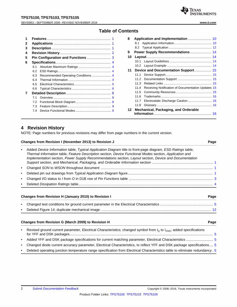
10.1 Layout GuidelinesFigure 15 demonstrates an example layout for the WSON package.
10.2 Layout Example
Figure 15. Layout Example for the WSON (DSK) Package
15
TPS75100, TPS75103, TPS75105www.ti.com SBVS080J –SEPTEMBER 2006–REVISED NOVEMBER 2016
Product Folder Links: TPS75100 TPS75103 TPS75105
Submit Documentation FeedbackCopyright © 2006–2016, Texas Instruments Incorporated
(1) For the most current package and ordering information see the Package Option Addendum at the end of this document, or see the TIweb site at www.ti.com.
(2) Default set currents from 3 mA to 10 mA in 1-mA increments are available through the use of innovative factory EEPROM programming.Minimum order quantities may apply. Contact factory for details and availability.
11 Device and Documentation Support
11.1 Device Support
11.1.1 Development SupportTwo evaluation modules (EVMs) are available to assist in the initial circuit performance evaluation using theTPS7510x. The TPS75105EVM-174 and TPS75105DSKEVM-529 evaluation modules (and related user guides)can be requested at the Texas Instruments website through the product folders or purchased directly from the TIeStore.
11.1.2 Device Nomenclature
PRODUCT ID OPTIONS (1) (2)
TPS7510x yyyzX is the nominal default diode output current (for example, 3 = 3 mA, 5 = 5 mA, and 0 = 10 mA).YYY is the package designator.Z is the reel quantity (R = 3000, T = 250).
11.2 Documentation Support
11.2.1 Related DocumentationFor related documentation see the following:• TPS75105EVM-174 Evaluation Module (SLVU182)• TPS75105DSKEVM-529 Evaluation Module (SLVU334)
11.3 Related LinksThe table below lists quick access links. Categories include technical documents, support and communityresources, tools and software, and quick access to sample or buy.
Table 3. Related Links
PARTS PRODUCT FOLDER SAMPLE & BUY TECHNICALDOCUMENTS
TOOLS &SOFTWARE
SUPPORT &COMMUNITY
TPS75100 Click here Click here Click here Click here Click hereTPS75103 Click here Click here Click here Click here Click hereTPS75105 Click here Click here Click here Click here Click here
11.4 Receiving Notification of Documentation UpdatesTo receive notification of documentation updates, navigate to the device product folder on ti.com. In the upperright corner, click on Alert me to register and receive a weekly digest of any product information that haschanged. For change details, review the revision history included in any revised document.
11.5 Community ResourcesThe following links connect to TI community resources. Linked contents are provided "AS IS" by the respectivecontributors. They do not constitute TI specifications and do not necessarily reflect TI's views; see TI's Terms ofUse.
TI E2E™ Online Community TI's Engineer-to-Engineer (E2E) Community. Created to foster collaborationamong engineers. At e2e.ti.com, you can ask questions, share knowledge, explore ideas and helpsolve problems with fellow engineers.
Design Support TI's Design Support Quickly find helpful E2E forums along with design support tools andcontact information for technical support.

16
TPS75100, TPS75103, TPS75105SBVS080J –SEPTEMBER 2006–REVISED NOVEMBER 2016 www.ti.com
Product Folder Links: TPS75100 TPS75103 TPS75105
Submit Documentation Feedback Copyright © 2006–2016, Texas Instruments Incorporated
11.6 TrademarksE2E is a trademark of Texas Instruments.All other trademarks are the property of their respective owners.
11.7 Electrostatic Discharge CautionThis integrated circuit can be damaged by ESD. Texas Instruments recommends that all integrated circuits be handled withappropriate precautions. Failure to observe proper handling and installation procedures can cause damage.
ESD damage can range from subtle performance degradation to complete device failure. Precision integrated circuits may be moresusceptible to damage because very small parametric changes could cause the device not to meet its published specifications.
11.8 GlossarySLYZ022 — TI Glossary.
This glossary lists and explains terms, acronyms, and definitions.
12 Mechanical, Packaging, and Orderable InformationThe following pages include mechanical, packaging, and orderable information. This information is the mostcurrent data available for the designated devices. This data is subject to change without notice and revision ofthis document. For browser-based versions of this data sheet, refer to the left-hand navigation.

PACKAGE OPTION ADDENDUM
www.ti.com 15-Apr-2017
Addendum-Page 1
PACKAGING INFORMATION
Orderable Device Status(1)
Package Type PackageDrawing
Pins PackageQty
Eco Plan(2)
Lead/Ball Finish(6)
MSL Peak Temp(3)
Op Temp (°C) Device Marking(4/5)
Samples
TPS75100DSKR ACTIVE SON DSK 10 3000 Green (RoHS& no Sb/Br)
CU NIPDAU Level-1-260C-UNLIM -40 to 85 SKX
TPS75100DSKT ACTIVE SON DSK 10 250 Green (RoHS& no Sb/Br)
CU NIPDAU Level-1-260C-UNLIM -40 to 85 SKX
TPS75100YFFR ACTIVE DSBGA YFF 9 3000 Green (RoHS& no Sb/Br)
SNAGCU Level-1-260C-UNLIM -40 to 85 FB
TPS75100YFFT ACTIVE DSBGA YFF 9 250 Green (RoHS& no Sb/Br)
SNAGCU Level-1-260C-UNLIM -40 to 85 FB
TPS75103YFFR ACTIVE DSBGA YFF 9 3000 Green (RoHS& no Sb/Br)
SNAGCU Level-1-260C-UNLIM -40 to 85 FC
TPS75103YFFT ACTIVE DSBGA YFF 9 250 Green (RoHS& no Sb/Br)
SNAGCU Level-1-260C-UNLIM -40 to 85 FC
TPS75105DSKR ACTIVE SON DSK 10 3000 Green (RoHS& no Sb/Br)
CU NIPDAU Level-1-260C-UNLIM -40 to 85 CHH
TPS75105DSKT ACTIVE SON DSK 10 250 Green (RoHS& no Sb/Br)
CU NIPDAU Level-1-260C-UNLIM -40 to 85 CHH
TPS75105YFFR ACTIVE DSBGA YFF 9 3000 Green (RoHS& no Sb/Br)
SNAGCU Level-1-260C-UNLIM -40 to 85 FE
TPS75105YFFT ACTIVE DSBGA YFF 9 250 Green (RoHS& no Sb/Br)
SNAGCU Level-1-260C-UNLIM -40 to 85 FE
(1) The marketing status values are defined as follows:ACTIVE: Product device recommended for new designs.LIFEBUY: TI has announced that the device will be discontinued, and a lifetime-buy period is in effect.NRND: Not recommended for new designs. Device is in production to support existing customers, but TI does not recommend using this part in a new design.PREVIEW: Device has been announced but is not in production. Samples may or may not be available.OBSOLETE: TI has discontinued the production of the device.
(2) Eco Plan - The planned eco-friendly classification: Pb-Free (RoHS), Pb-Free (RoHS Exempt), or Green (RoHS & no Sb/Br) - please check http://www.ti.com/productcontent for the latest availabilityinformation and additional product content details.TBD: The Pb-Free/Green conversion plan has not been defined.Pb-Free (RoHS): TI's terms "Lead-Free" or "Pb-Free" mean semiconductor products that are compatible with the current RoHS requirements for all 6 substances, including the requirement thatlead not exceed 0.1% by weight in homogeneous materials. Where designed to be soldered at high temperatures, TI Pb-Free products are suitable for use in specified lead-free processes.Pb-Free (RoHS Exempt): This component has a RoHS exemption for either 1) lead-based flip-chip solder bumps used between the die and package, or 2) lead-based die adhesive used betweenthe die and leadframe. The component is otherwise considered Pb-Free (RoHS compatible) as defined above.Green (RoHS & no Sb/Br): TI defines "Green" to mean Pb-Free (RoHS compatible), and free of Bromine (Br) and Antimony (Sb) based flame retardants (Br or Sb do not exceed 0.1% by weightin homogeneous material)

PACKAGE OPTION ADDENDUM
www.ti.com 15-Apr-2017
Addendum-Page 2
(3) MSL, Peak Temp. - The Moisture Sensitivity Level rating according to the JEDEC industry standard classifications, and peak solder temperature.
(4) There may be additional marking, which relates to the logo, the lot trace code information, or the environmental category on the device.
(5) Multiple Device Markings will be inside parentheses. Only one Device Marking contained in parentheses and separated by a "~" will appear on a device. If a line is indented then it is a continuationof the previous line and the two combined represent the entire Device Marking for that device.
(6) Lead/Ball Finish - Orderable Devices may have multiple material finish options. Finish options are separated by a vertical ruled line. Lead/Ball Finish values may wrap to two lines if the finishvalue exceeds the maximum column width.
Important Information and Disclaimer:The information provided on this page represents TI's knowledge and belief as of the date that it is provided. TI bases its knowledge and belief on informationprovided by third parties, and makes no representation or warranty as to the accuracy of such information. Efforts are underway to better integrate information from third parties. TI has taken andcontinues to take reasonable steps to provide representative and accurate information but may not have conducted destructive testing or chemical analysis on incoming materials and chemicals.TI and TI suppliers consider certain information to be proprietary, and thus CAS numbers and other limited information may not be available for release.
In no event shall TI's liability arising out of such information exceed the total purchase price of the TI part(s) at issue in this document sold by TI to Customer on an annual basis.

TAPE AND REEL INFORMATION
*All dimensions are nominal
Device PackageType
PackageDrawing
Pins SPQ ReelDiameter
(mm)
ReelWidth
W1 (mm)
A0(mm)
B0(mm)
K0(mm)
P1(mm)
W(mm)
Pin1Quadrant
TPS75100DSKR SON DSK 10 3000 179.0 8.4 2.73 2.73 0.8 4.0 8.0 Q2
TPS75100DSKT SON DSK 10 250 179.0 8.4 2.73 2.73 0.8 4.0 8.0 Q2
TPS75100YFFR DSBGA YFF 9 3000 180.0 8.4 1.34 1.34 0.81 4.0 8.0 Q1
TPS75100YFFT DSBGA YFF 9 250 180.0 8.4 1.34 1.34 0.81 4.0 8.0 Q1
TPS75103YFFR DSBGA YFF 9 3000 180.0 8.4 1.45 1.45 0.8 4.0 8.0 Q1
TPS75103YFFT DSBGA YFF 9 250 180.0 8.4 1.45 1.45 0.8 4.0 8.0 Q1
TPS75105DSKR SON DSK 10 3000 179.0 8.4 2.73 2.73 0.8 4.0 8.0 Q2
TPS75105DSKT SON DSK 10 250 179.0 8.4 2.73 2.73 0.8 4.0 8.0 Q2
TPS75105YFFR DSBGA YFF 9 3000 180.0 8.4 1.45 1.45 0.8 4.0 8.0 Q1
TPS75105YFFT DSBGA YFF 9 250 180.0 8.4 1.45 1.45 0.8 4.0 8.0 Q1
PACKAGE MATERIALS INFORMATION
www.ti.com 3-Aug-2017
Pack Materials-Page 1

*All dimensions are nominal
Device Package Type Package Drawing Pins SPQ Length (mm) Width (mm) Height (mm)
TPS75100DSKR SON DSK 10 3000 203.0 203.0 35.0
TPS75100DSKT SON DSK 10 250 203.0 203.0 35.0
TPS75100YFFR DSBGA YFF 9 3000 182.0 182.0 20.0
TPS75100YFFT DSBGA YFF 9 250 182.0 182.0 20.0
TPS75103YFFR DSBGA YFF 9 3000 210.0 185.0 35.0
TPS75103YFFT DSBGA YFF 9 250 210.0 185.0 35.0
TPS75105DSKR SON DSK 10 3000 203.0 203.0 35.0
TPS75105DSKT SON DSK 10 250 203.0 203.0 35.0
TPS75105YFFR DSBGA YFF 9 3000 210.0 185.0 35.0
TPS75105YFFT DSBGA YFF 9 250 210.0 185.0 35.0
PACKAGE MATERIALS INFORMATION
www.ti.com 3-Aug-2017
Pack Materials-Page 2

www.ti.com
PACKAGE OUTLINE
C0.625 MAX
0.300.12
0.8TYP
0.8 TYP
0.4 TYP
0.4 TYP
9X 0.30.2
B E A
D
DSBGA - 0.625 mm max heightYFF0009DIE SIZE BALL GRID ARRAY
4219552/A 05/2016
NOTES: 1. All linear dimensions are in millimeters. Any dimensions in parenthesis are for reference only. Dimensioning and tolerancing per ASME Y14.5M.2. This drawing is subject to change without notice.
BALL A1CORNER
SEATING PLANE
BALL TYP 0.05 C
B
1 2 3
0.015 C A B
SYMM
SYMM
A
C
SCALE 10.000
D: Max =
E: Max =
1.238 mm, Min =
1.238 mm, Min =
1.178 mm
1.178 mm

www.ti.com
EXAMPLE BOARD LAYOUT
9X ( 0.23)
(0.4) TYP
(0.4) TYP
( 0.23)METAL
0.05 MAX
SOLDER MASKOPENING
METAL UNDERSOLDER MASK
( 0.23)SOLDER MASKOPENING
0.05 MIN
DSBGA - 0.625 mm max heightYFF0009DIE SIZE BALL GRID ARRAY
4219552/A 05/2016
NOTES: (continued) 3. Final dimensions may vary due to manufacturing tolerance considerations and also routing constraints. For more information, see Texas Instruments literature number SNVA009 (www.ti.com/lit/snva009).
SYMM
SYMM
LAND PATTERN EXAMPLESCALE:30X
C
1 2 3A
B
NON-SOLDER MASKDEFINED
(PREFERRED)
SOLDER MASK DETAILSNOT TO SCALE
SOLDER MASKDEFINED

www.ti.com
EXAMPLE STENCIL DESIGN
(0.4) TYP
(0.4) TYP
9X ( 0.25) (R0.05) TYP
METALTYP
DSBGA - 0.625 mm max heightYFF0009DIE SIZE BALL GRID ARRAY
4219552/A 05/2016
NOTES: (continued) 4. Laser cutting apertures with trapezoidal walls and rounded corners may offer better paste release.
SYMM
SYMM
C
1 2 3A
B
SOLDER PASTE EXAMPLEBASED ON 0.1 mm THICK STENCIL
SCALE:30X


IMPORTANT NOTICE
Texas Instruments Incorporated (TI) reserves the right to make corrections, enhancements, improvements and other changes to itssemiconductor products and services per JESD46, latest issue, and to discontinue any product or service per JESD48, latest issue. Buyersshould obtain the latest relevant information before placing orders and should verify that such information is current and complete.TI’s published terms of sale for semiconductor products (http://www.ti.com/sc/docs/stdterms.htm) apply to the sale of packaged integratedcircuit products that TI has qualified and released to market. Additional terms may apply to the use or sale of other types of TI products andservices.Reproduction of significant portions of TI information in TI data sheets is permissible only if reproduction is without alteration and isaccompanied by all associated warranties, conditions, limitations, and notices. TI is not responsible or liable for such reproduceddocumentation. Information of third parties may be subject to additional restrictions. Resale of TI products or services with statementsdifferent from or beyond the parameters stated by TI for that product or service voids all express and any implied warranties for theassociated TI product or service and is an unfair and deceptive business practice. TI is not responsible or liable for any such statements.Buyers and others who are developing systems that incorporate TI products (collectively, “Designers”) understand and agree that Designersremain responsible for using their independent analysis, evaluation and judgment in designing their applications and that Designers havefull and exclusive responsibility to assure the safety of Designers' applications and compliance of their applications (and of all TI productsused in or for Designers’ applications) with all applicable regulations, laws and other applicable requirements. Designer represents that, withrespect to their applications, Designer has all the necessary expertise to create and implement safeguards that (1) anticipate dangerousconsequences of failures, (2) monitor failures and their consequences, and (3) lessen the likelihood of failures that might cause harm andtake appropriate actions. Designer agrees that prior to using or distributing any applications that include TI products, Designer willthoroughly test such applications and the functionality of such TI products as used in such applications.TI’s provision of technical, application or other design advice, quality characterization, reliability data or other services or information,including, but not limited to, reference designs and materials relating to evaluation modules, (collectively, “TI Resources”) are intended toassist designers who are developing applications that incorporate TI products; by downloading, accessing or using TI Resources in anyway, Designer (individually or, if Designer is acting on behalf of a company, Designer’s company) agrees to use any particular TI Resourcesolely for this purpose and subject to the terms of this Notice.TI’s provision of TI Resources does not expand or otherwise alter TI’s applicable published warranties or warranty disclaimers for TIproducts, and no additional obligations or liabilities arise from TI providing such TI Resources. TI reserves the right to make corrections,enhancements, improvements and other changes to its TI Resources. TI has not conducted any testing other than that specificallydescribed in the published documentation for a particular TI Resource.Designer is authorized to use, copy and modify any individual TI Resource only in connection with the development of applications thatinclude the TI product(s) identified in such TI Resource. NO OTHER LICENSE, EXPRESS OR IMPLIED, BY ESTOPPEL OR OTHERWISETO ANY OTHER TI INTELLECTUAL PROPERTY RIGHT, AND NO LICENSE TO ANY TECHNOLOGY OR INTELLECTUAL PROPERTYRIGHT OF TI OR ANY THIRD PARTY IS GRANTED HEREIN, including but not limited to any patent right, copyright, mask work right, orother intellectual property right relating to any combination, machine, or process in which TI products or services are used. Informationregarding or referencing third-party products or services does not constitute a license to use such products or services, or a warranty orendorsement thereof. Use of TI Resources may require a license from a third party under the patents or other intellectual property of thethird party, or a license from TI under the patents or other intellectual property of TI.TI RESOURCES ARE PROVIDED “AS IS” AND WITH ALL FAULTS. TI DISCLAIMS ALL OTHER WARRANTIES ORREPRESENTATIONS, EXPRESS OR IMPLIED, REGARDING RESOURCES OR USE THEREOF, INCLUDING BUT NOT LIMITED TOACCURACY OR COMPLETENESS, TITLE, ANY EPIDEMIC FAILURE WARRANTY AND ANY IMPLIED WARRANTIES OFMERCHANTABILITY, FITNESS FOR A PARTICULAR PURPOSE, AND NON-INFRINGEMENT OF ANY THIRD PARTY INTELLECTUALPROPERTY RIGHTS. TI SHALL NOT BE LIABLE FOR AND SHALL NOT DEFEND OR INDEMNIFY DESIGNER AGAINST ANY CLAIM,INCLUDING BUT NOT LIMITED TO ANY INFRINGEMENT CLAIM THAT RELATES TO OR IS BASED ON ANY COMBINATION OFPRODUCTS EVEN IF DESCRIBED IN TI RESOURCES OR OTHERWISE. IN NO EVENT SHALL TI BE LIABLE FOR ANY ACTUAL,DIRECT, SPECIAL, COLLATERAL, INDIRECT, PUNITIVE, INCIDENTAL, CONSEQUENTIAL OR EXEMPLARY DAMAGES INCONNECTION WITH OR ARISING OUT OF TI RESOURCES OR USE THEREOF, AND REGARDLESS OF WHETHER TI HAS BEENADVISED OF THE POSSIBILITY OF SUCH DAMAGES.Unless TI has explicitly designated an individual product as meeting the requirements of a particular industry standard (e.g., ISO/TS 16949and ISO 26262), TI is not responsible for any failure to meet such industry standard requirements.Where TI specifically promotes products as facilitating functional safety or as compliant with industry functional safety standards, suchproducts are intended to help enable customers to design and create their own applications that meet applicable functional safety standardsand requirements. Using products in an application does not by itself establish any safety features in the application. Designers mustensure compliance with safety-related requirements and standards applicable to their applications. Designer may not use any TI products inlife-critical medical equipment unless authorized officers of the parties have executed a special contract specifically governing such use.Life-critical medical equipment is medical equipment where failure of such equipment would cause serious bodily injury or death (e.g., lifesupport, pacemakers, defibrillators, heart pumps, neurostimulators, and implantables). Such equipment includes, without limitation, allmedical devices identified by the U.S. Food and Drug Administration as Class III devices and equivalent classifications outside the U.S.TI may expressly designate certain products as completing a particular qualification (e.g., Q100, Military Grade, or Enhanced Product).Designers agree that it has the necessary expertise to select the product with the appropriate qualification designation for their applicationsand that proper product selection is at Designers’ own risk. Designers are solely responsible for compliance with all legal and regulatoryrequirements in connection with such selection.Designer will fully indemnify TI and its representatives against any damages, costs, losses, and/or liabilities arising out of Designer’s non-compliance with the terms and provisions of this Notice.
Mailing Address: Texas Instruments, Post Office Box 655303, Dallas, Texas 75265Copyright © 2017, Texas Instruments Incorporated