Embed Size (px)
Citation preview

Copyright © 2017, Texas Instruments Incorporated
VDD
VGVS VD
REG
Vout
Copyright © 2017, Texas Instruments Incorporated
VDD
VG VSVD
REG
Product
Folder
Order
Now
Technical
Documents
Tools &
Software
Support &Community
An IMPORTANT NOTICE at the end of this data sheet addresses availability, warranty, changes, use in safety-critical applications,intellectual property matters and other important disclaimers. PRODUCTION DATA.
UCC24612SLUSCM5A –AUGUST 2017–REVISED FEBRUARY 2018
UCC24612 High Frequency Synchronous Rectifier Controller
1
1 Features1• Supports Topologies such as Active Clamp
Flyback, QR, DCM, CCM Flyback and LLC• MOSFET VDS Sensing up to 230 V• Operating Frequency Up to 1 MHz
– 1 MHz for UCC24612-1– 800 kHz for UCC24612-2
• Wide VDD Range Allows for Direct Bias from 5-Vto 28-V Output Systems
• 4-A Sink, 1-A Source Gate Driver withProportional Gate Drive
• Adaptive Minimum Off-time for Increased NoiseImmunity
• Cycle Limit Pre-Turn-off Improves Efficiency inCCM
• High or Low-Side Configurable• Automatic Light-Load and Sleep-Mode
Management with 320-µA standby current• 16-ns Typical Turnoff Propagation Delay• 9.5-V Gate Drive Clamp for Reduced Driving Loss
2 Applications• AC-to-DC Adapters• USB Type-C and Power Delivery AC Adapters• Server and Telecom Power Supply• AC-to-DC Auxiliary Power Supply
3 DescriptionUCC24612 is a high performance synchronousrectifier controller and driver for standard and logic-level N-channel MOSFET power devices. Byimplementing a near-ideal diode emulationUCC24612 reduces losses of the output rectifier andindirectly the primary side losses. The drain to source(VDS) sensing control scheme allows UCC24612 towork with multiple topologies, such as Active ClampFlyback, QR/DCM/CCM Flyback and LLC, et.
Integrated features simplify the design effort, enablingUCC24612 to excel in a variety of applications andfrequencies. The wide operating VDD and VD voltageranges enable simple implementation in systems withoutputs up to 28 V. Efficiency and noise immunity isenhanced with adaptive minimum off-time. VariantsUCC24612-1 and UCC24612-2 offer differentminimum on-times to provide additional noiseimmunity. Robust operation in continuous conductionmode (CCM) is further enhanced with proportionalgate-drive and CCM cycle limit pre-turn-off.
UCC24612 has multiple features that improveefficiency. The fast comparator with short propagationdelays reduces switching loss. The 9.5-V gate driveclamp reduces MOSFET driving losses. Frequencydependent standby modes further decreases standbypower. These features help UCC24612 be part of agreater system that meets stringent efficiencystandards such as Department of Energy (DoE) LevelVI and Code of Conduct (CoC) Tier 2.
UCC24612 is available in a SOT23-5 package.
Device Information(1)
PART NUMBER PACKAGE BODY SIZE (NOM)UCC24612 SOT23 (5) 3.00 mm × 3.00 mm
(1) For all available packages, see the orderable addendum atthe end of the data sheet.
Flyback with High-Side SRFlyback with Low-Side SR
2
UCC24612SLUSCM5A –AUGUST 2017–REVISED FEBRUARY 2018 www.ti.com
Submit Documentation Feedback Copyright © 2017–2018, Texas Instruments Incorporated
Table of Contents1 Features .................................................................. 12 Applications ........................................................... 13 Description ............................................................. 14 Revision History..................................................... 25 Pin Configuration and Functions ......................... 36 Specifications......................................................... 3
6.1 Absolute Maximum Ratings ...................................... 36.2 ESD Ratings ............................................................ 46.3 Recommended Operating Conditions....................... 56.4 Thermal Information .................................................. 56.5 Electrical Characteristics........................................... 66.6 Timing Requirements ................................................ 76.7 Typical Characteristics .............................................. 8
7 Detailed Description ............................................ 107.1 Overview ................................................................. 107.2 Functional Block Diagram ....................................... 10
7.3 Feature Description................................................. 117.4 Device Functional Modes........................................ 22
8 Application and Implementation ........................ 238.1 Application Information............................................ 238.2 Typical Application ................................................. 23
9 Power Supply Recommendations ...................... 2910 PCB Layout .......................................................... 31
10.1 Layout Guidelines ................................................. 3110.2 Layout Example .................................................... 31
11 Device and Documentation Support ................. 3211.1 Community Resources.......................................... 3211.2 Trademarks ........................................................... 3211.3 Electrostatic Discharge Caution............................ 3211.4 Glossary ................................................................ 32
12 Mechanical, Packaging, and OrderableInformation ........................................................... 32
4 Revision History
DATE REVISION NOTESFebruary 2018 A Initial release.
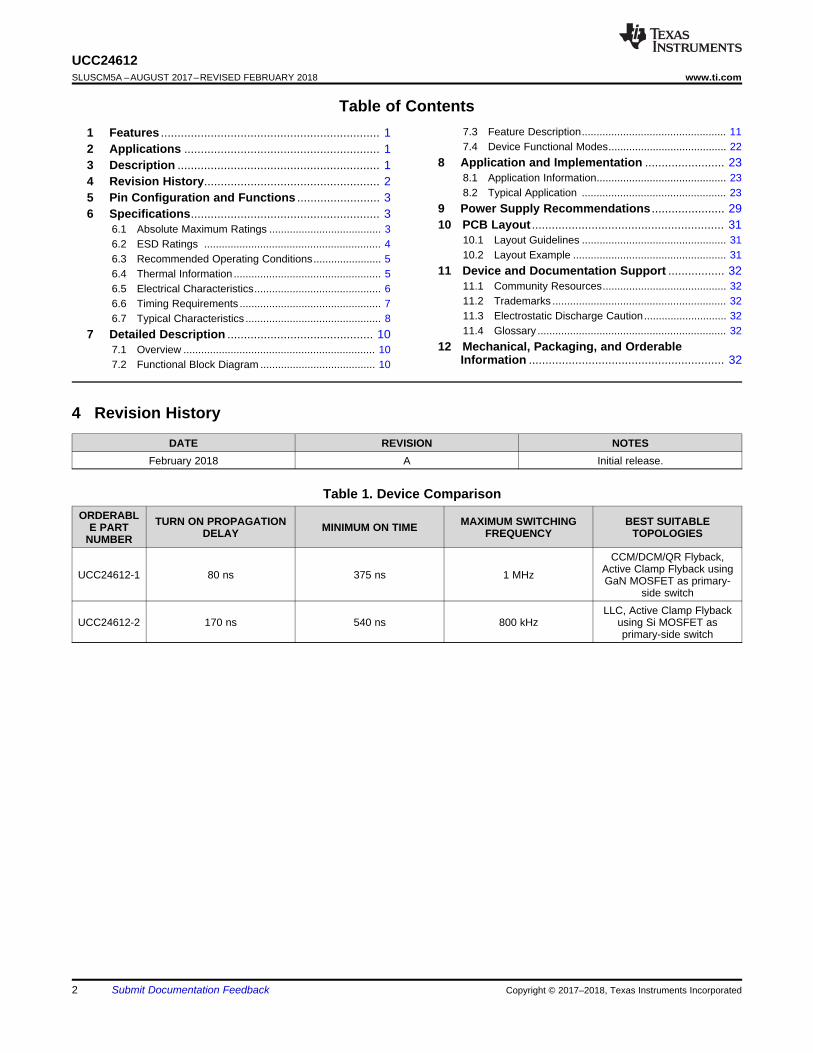
Table 1. Device ComparisonORDERABL
E PARTNUMBER
TURN ON PROPAGATIONDELAY MINIMUM ON TIME MAXIMUM SWITCHING
FREQUENCYBEST SUITABLE
TOPOLOGIES
UCC24612-1 80 ns 375 ns 1 MHz
CCM/DCM/QR Flyback,Active Clamp Flyback usingGaN MOSFET as primary-
side switch
UCC24612-2 170 ns 540 ns 800 kHzLLC, Active Clamp Flyback
using Si MOSFET asprimary-side switch

1
2
3
5
4
UCC24612(DBV)
VS
REG
VD
VDD
(TOP VIEW)
VG
3
UCC24612www.ti.com SLUSCM5A –AUGUST 2017–REVISED FEBRUARY 2018
Submit Documentation FeedbackCopyright © 2017–2018, Texas Instruments Incorporated
5 Pin Configuration and Functions
5-Pin SOT-23
Pin FunctionsPIN
I/O DESCRIPTIONNAME NO.
REG 3 O REG is the device bias pin. An internal linear regulator from VDD to REG generates a well regulated9.5-V voltage. It is recommend to put a 2.2-µF bypass capacitor from REG pin to VS pin.
VD 5 I MOSFET drain voltage sensing input. Connect this pin to SR MOSFET drain pin. The layout shouldavoid sharing the VD pin trace with the power path to minimize the impact of parasitic inductance.
VDD 4 IInternal linear regulator input. Connect this pin to the output voltage when in low-side SRconfiguration. Use R-C-D circuit or other circuits to generate bias voltage from SR MOSFET drainwhen using high-side SR configuration, referring to Power Supply Recommendations for details.
VG 1 O
VG (controlled MOSFET gate drive), connect VG to the gate of the controlled MOSFET through asmall series resistor using short PC board tracks to achieve optimal switching performance. The VGoutput can achieve >1-A peak source current when High and >4-A peak sink current when Low whenconnected to a large N-channel power MOSFET. Due to the weak internal pull up after initial fast turnon, avoid putting a resistor less than 50 kΩ between VG to VS .
VS 2 -VS is the internal ground reference of the UCC24612. It is also used to sense the voltage drop acrossthe SR MOSFET. The layout should avoid sharing the VS pin trace with the power path to minimizethe impact of parasitic inductance.
(1) Stresses beyond those listed under Absolute Maximum Ratings may cause permanent damage to the device. These are stress ratingsonly, which do not imply functional operation of the device at these or any other conditions beyond those indicated under RecommendedOperating Conditions. Exposure to absolute-maximum-rated conditions for extended periods may affect device reliability.
(2) Input voltages more negative than indicated may exist on any listed pin without excess stress or damage to the device if the pin’s inputcurrent magnitude is limited to less than -10mA.
(3) In normal use, VG is connected to the gate of a power MOSFET through a small resistor. When used this way, VG current is limited bythe UCC24612 and no absolute maximum output current considerations are required. The series resistor shall be selected to minimizeovershoot and ringing due to series inductance of the VG output and power-MOSFET gate-drive loop. Continuous VG current is subjectto the maximum operating junction temperature limitation.
6 Specifications
6.1 Absolute Maximum Ratingsover operating free-air temperature range (unless otherwise noted) (1)
MIN MAX UNIT
Input voltage (2)
VDD –0.3 30 VVD –0.7 230 VVG –0.3 VREG VVD for IVD ≤ –10 mA –1.0 230 VREG 12 V
Output current, peak VG (3) pulsed, tPULSE ≤ 4 ms, duty cycle ≤ 1% ±4 ATJ Operating junction temperature –40 125 °CTstg Storage temperature –65 150 °C

4
UCC24612SLUSCM5A –AUGUST 2017–REVISED FEBRUARY 2018 www.ti.com
Submit Documentation Feedback Copyright © 2017–2018, Texas Instruments Incorporated
(1) JEDEC document JEP155 states that 500-V HBM allows safe manufacturing with a standard ESD control process.(2) JEDEC document JEP157 states that 250-V CDM allows safe manufacturing with a standard ESD control process.
6.2 ESD RatingsVALUE UNIT
V(ESD) Electrostatic discharge
Human body model (HBM), per ANSI/ESDA/JEDEC JS-001, all pins,except pin 5 (1) ±2,000 V
Human body model (HBM), per ANSI/ESDA/JEDEC JS-001, pin 5 (1) ±1,500 VCharged device model (CDM), per JEDEC specification JESD22-C101,all pins (2) ±500 V

5
UCC24612www.ti.com SLUSCM5A –AUGUST 2017–REVISED FEBRUARY 2018
Submit Documentation FeedbackCopyright © 2017–2018, Texas Instruments Incorporated
6.3 Recommended Operating Conditionsover operating free-air temperature range (unless otherwise noted)
MIN NOM MAX UNITVVDD VDD input voltage 4 28 VCVDD VDD bypass capacitor 1 µFCREG REG bypass capacitor 1.5 2.2 µFTJ Junction temperature –40 125 °C
fS_MAXMaximum switching frequency UCC24612-1 770 1000
kHzMaximum switching frequency UCC24612-2 625 800
(1) For more information about traditional and new thermal metrics, see the the Semiconductor and IC Package Thermal Metrics applicationreport, SPRA953.
6.4 Thermal Information
THERMAL METRIC (1)UCC24612
UNITDBV (SOT23-5)5 PINs
RθJA Junction-to-ambient thermal resistance 206.6 °C/WRθJC(top) Junction-to-case (top) thermal resistance 97.6 °C/WRθJB Junction-to-board thermal resistance 44.2 °C/WψJT Junction-to-top characterization parameter 9.9 °C/WψJB Junction-to-board characterization parameter 43.7 °C/W

6
UCC24612SLUSCM5A –AUGUST 2017–REVISED FEBRUARY 2018 www.ti.com
Submit Documentation Feedback Copyright © 2017–2018, Texas Instruments Incorporated
(1) Specified by design
6.5 Electrical CharacteristicsAt VDD = 12 VDC, CVG = 0 pF, CREG = 2.2 µF, −40°C ≤ TJ = TA ≤ +125°C, all voltages are with respect to VS, and currents arepositive into and negative out of the specified terminal, unless otherwise noted. Typical values are at TJ = +25°C.
PARAMETER TEST CONDITIONS MIN TYP MAX UNITBIAS SUPPLYIVDDSTART VDD current, REG undervoltage VDD = 4 V, VD = 0 V 50 105 150 μA
IVDDRUN VDD current, runVDD = 12 V 0.5 0.92 1.5 mAVDD = 5 V 0.5 0.9 1.5 mA
IVDDSTBY VDD current, standby modeVDD = 12 V, VD = 1 V 200 390 650 μAVDD = 5 V, VD = 1 V 200 320 500 μA
UNDERVOLTAGE LOCKOUT (UVLO)VREGON REG turn-on threshold Turn-on detected by IVDD rising 4.15 4.5 4.87 VVREGOFF REG turn-off threshold Turn-off detected by IVDD falling 3.65 4 4.25 VVREGHYST UVLO hysteresis VREGHYST = VREGON – VREGOFF 0.425 0.5 0.575 VMOSFET VOLTAGE SENSINGVTHVGON VG turn-on threshold VD falling, TJ = 25°C –300 –240 –175 mV
VTHVGOFF VG turn-off thresholdVD rising, TJ = 25°C –20 -9 –2
mVVD rising, –40°C ≤TJ ≤ 125°C –30 –9 –2
VTHARM VG re-arming threshold VD rising 0.4 0.5 0.6 V
IVDBIAS_ONVD pin bias current when VG ishigh (SR is on) VVD = –50 mV, VVG = VGH –1 0 1 µA
IVDBIAS_OFFVD pin bias current when VG islow (SR is off)
VVD = –150 mV, VVG = VGL, TJ =25°C –6 –2
µAVVD = –150 mV, VVG = VGL, –40°C≤TJ ≤ 125°C –10
IVDLK VD pin leakage current VVD = 200 V 0.06 2 µAGATE DRIVERRSOURCE VG pull-up resistance IVG = –20 mA 5.7 10 Ω
RSINK VG pull-down resistance IVG = 100 mA 0.45 1 Ω
VGH VG clamp level 8.55 9.4 10.26 VVGL VG output low voltage IVG = 100 mA, VDD = 12 V 60 150 mVVOLGUV VG output low voltage in UVLO IVG = 25 mA, VDD = 4 V 0.7 V
IVGPUGate driver maximum sourcecurrent 1 (1) A
IVGPD Gate driver maximum sink current (1) 4 AREG SUPPLYVREG REG pin regulation level ILOAD_REG = 0 mA 8.55 9.4 10.26 VVREGLG Load regulation on REG ILOAD_REG= 10 mA to 0 mA 0.016 0.1 V
VREGDOREG drop-out on pass-throughmode VDD = 5 V, ILOAD_REG= 10 mA 0.28 0.45 V
IREGSC REG short-circuit current VREG = 0 V 1 5.2 15 mAIREGLIM REG current limit VREG = 8 V 25 42 62 mA
7
UCC24612www.ti.com SLUSCM5A –AUGUST 2017–REVISED FEBRUARY 2018
Submit Documentation FeedbackCopyright © 2017–2018, Texas Instruments Incorporated
(1) Specified by design
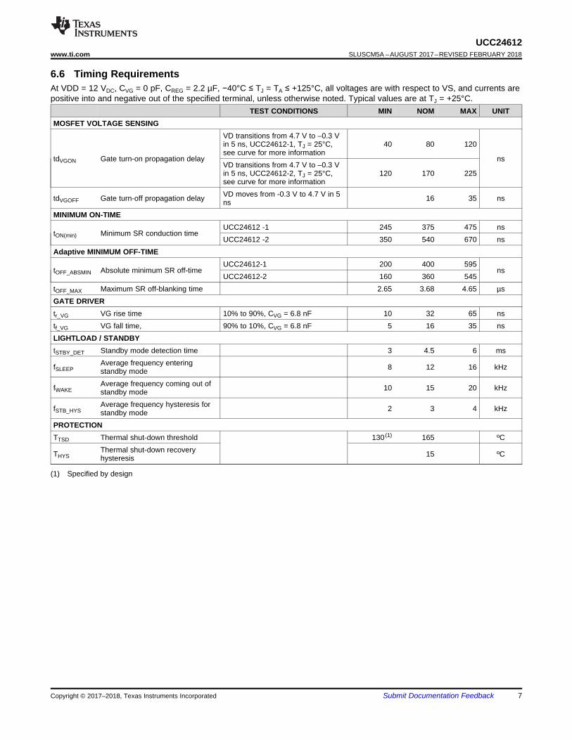
6.6 Timing RequirementsAt VDD = 12 VDC, CVG = 0 pF, CREG = 2.2 µF, −40°C ≤ TJ = TA ≤ +125°C, all voltages are with respect to VS, and currents arepositive into and negative out of the specified terminal, unless otherwise noted. Typical values are at TJ = +25°C.
TEST CONDITIONS MIN NOM MAX UNITMOSFET VOLTAGE SENSING
tdVGON Gate turn-on propagation delay
VD transitions from 4.7 V to –0.3 Vin 5 ns, UCC24612-1, TJ = 25°C,see curve for more information
40 80 120
nsVD transitions from 4.7 V to –0.3 Vin 5 ns, UCC24612-2, TJ = 25°C,see curve for more information
120 170 225
tdVGOFF Gate turn-off propagation delay VD moves from -0.3 V to 4.7 V in 5ns 16 35 ns
MINIMUM ON-TIME
tON(min) Minimum SR conduction timeUCC24612 -1 245 375 475 nsUCC24612 -2 350 540 670 ns
Adaptive MINIMUM OFF-TIME
tOFF_ABSMIN Absolute minimum SR off-timeUCC24612-1 200 400 595
nsUCC24612-2 160 360 545
tOFF_MAX Maximum SR off-blanking time 2.65 3.68 4.65 µsGATE DRIVERtr_VG VG rise time 10% to 90%, CVG = 6.8 nF 10 32 65 nstf_VG VG fall time, 90% to 10%, CVG = 6.8 nF 5 16 35 nsLIGHTLOAD / STANDBYtSTBY_DET Standby mode detection time 3 4.5 6 ms
fSLEEPAverage frequency enteringstandby mode 8 12 16 kHz
fWAKEAverage frequency coming out ofstandby mode 10 15 20 kHz
fSTB_HYSAverage frequency hysteresis forstandby mode 2 3 4 kHz
PROTECTIONTTSD Thermal shut-down threshold 130 (1) 165 ºC
THYSThermal shut-down recoveryhysteresis 15 ºC
Junction Temperature (oC)
Pro
port
iona
l Gat
e-dr
ive
Thr
esho
ld (
mV
)
-40 -20 0 20 40 60 80 100 120 140-100
-95
-90
-85
-80
-75
-70
-65
-60
-55
-50
-45
-40
-35
D001
MeanMinimumMaximum
Junction Temperature (oC)
RE
G P
in R
egul
atio
n Le
vel V
RE
G (
V)
-40 -20 0 20 40 60 80 100 120 1409
9.05
9.1
9.15
9.2
9.25
9.3
9.35
9.4
9.45
9.5
D001
ILOAD_REG = 0 mAILOAD_REG = 10 mA
Junction Temperature (oC)
SR
Tur
n-of
f Thr
esho
ld V
TH
VG
OF
F (
mV
)
-40 -20 0 20 40 60 80 100 120 140-12.5
-12
-11.5
-11
-10.5
-10
-9.5
-9
-8.5
-8
D001
5.5-V VDD12-V VDD
Junction Temperature (oC)
SR
Tur
n-on
Thr
esho
ld V
TH
VG
ON
(m
V)
-40 -20 0 20 40 60 80 100 120 140-500
-450
-400
-350
-300
-250
-200
-150
-100
-50
0
D001
Junction Temperature (oC)
UV
LO T
hres
hold
s (V
)
-40 -20 0 20 40 60 80 100 120 1403.9
3.95
4
4.05
4.1
4.15
4.2
4.25
4.3
4.35
4.4
4.45
4.5
D001
UVLO ONUVLO OFF
Junction Temperature (oC)
VD
D C
urre
nt, R
UN
(IV
DD
RU
N)
(mA
)
-40 -20 0 20 40 60 80 100 120 1400.5
0.6
0.7
0.8
0.9
1
1.1
1.2
1.3
1.4
1.5
D001
5-V VDD12-V VDD24-V VDD
8
UCC24612SLUSCM5A –AUGUST 2017–REVISED FEBRUARY 2018 www.ti.com
Submit Documentation Feedback Copyright © 2017–2018, Texas Instruments Incorporated
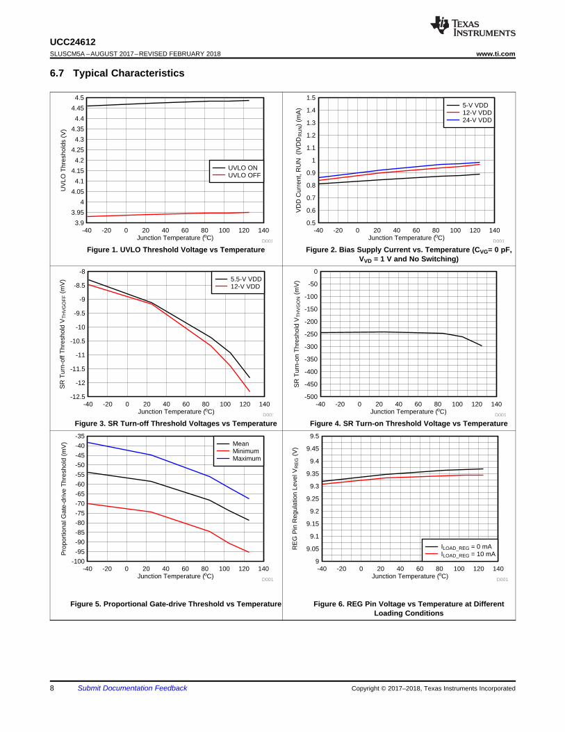
6.7 Typical Characteristics
Figure 1. UVLO Threshold Voltage vs Temperature Figure 2. Bias Supply Current vs. Temperature (CVG= 0 pF,VVD = 1 V and No Switching)
Figure 3. SR Turn-off Threshold Voltages vs Temperature Figure 4. SR Turn-on Threshold Voltage vs Temperature
Figure 5. Proportional Gate-drive Threshold vs Temperature Figure 6. REG Pin Voltage vs Temperature at DifferentLoading Conditions

Junction Temperature (oC)
Tur
n-of
f Pro
paga
tion
Del
ay td
VG
OF
F (
ns)
-40 -20 0 20 40 60 80 100 120 14010
11
12
13
14
15
16
17
18
19
20
D001Junction Temperature (oC)
VD
D S
tand
by M
ode
Cur
rent
IVD
DS
TB
Y (P
A)
-40 -20 0 20 40 60 80 100 120 140100
150
200
250
300
350
400
450
500
550
600
D001
VDD = 12 VVDD = 5 V
Junction Temperature (oC)
Tur
n-on
Bla
nkin
g T
ime
t ON
(min
) (ns
)
-40 -20 0 20 40 60 80 100 120 140360
380
400
420
440
460
480
500
520
540
560
D001
UCC24612-1UCC24612-2
Junction Temperature (oC)
Tur
n-on
Pro
paga
tion
Del
ay td
VG
ON (
ns)
-40 -20 0 20 40 60 80 100 120 14060
80
100
120
140
160
180
200
D001
UCC24612-1UCC24612-2
Junction Temperature (oC)
RE
G D
rop-
out i
n P
ass-
thro
ugh
Mod
e V
RE
GD
O (
V)
-60 -30 0 30 60 90 120 1500.18
0.2
0.22
0.24
0.26
0.28
0.3
0.32
0.34
0.36
0.38
0.4
D001
Junction Temperature (oC)
Tur
n-of
f Bla
nkin
g T
ime
(Ps)
-40 -20 0 20 40 60 80 100 120 1400
0.5
1
1.5
2
2.5
3
3.5
4
D001
tOFF_MAXtOFF_ABSMIN
9
UCC24612www.ti.com SLUSCM5A –AUGUST 2017–REVISED FEBRUARY 2018
Submit Documentation FeedbackCopyright © 2017–2018, Texas Instruments Incorporated
Typical Characteristics (continued)
Figure 7. REG Drop-out in Pass-through Mode vsTemperature, ILOAD_REG = 10 mA
Figure 8. Abs. Minimum Turn-off Blanking Time andMaximum Turn-off Blanking Time vs Temperature
Figure 9. Turn-On Blanking Time vs Temperature Figure 10. SR Turn-on Delay Time vs Temperature
Figure 11. SR Turn-off Propagation Delay vs Temperature Figure 12. Standby Current vs Temperature
REGVDD
VD
START
TSD
VG
VSAdaptive TOFF
& DCM ring rejection
VTHVGON
S Q
QR
VTHVGOFF
VTHREG
Prop-DRV threshold
9.5-V Linear Regulator
REG UVLO
POWER & FAULT MANGEMENT PROPORTIONAL
GATE DRIVE CONTROL
GATE DRIVER
+
±
+
±
Turn On Blanking
Copyright © 2018, Texas Instruments Incorporated
10
UCC24612SLUSCM5A –AUGUST 2017–REVISED FEBRUARY 2018 www.ti.com
Submit Documentation Feedback Copyright © 2017–2018, Texas Instruments Incorporated
7 Detailed Description
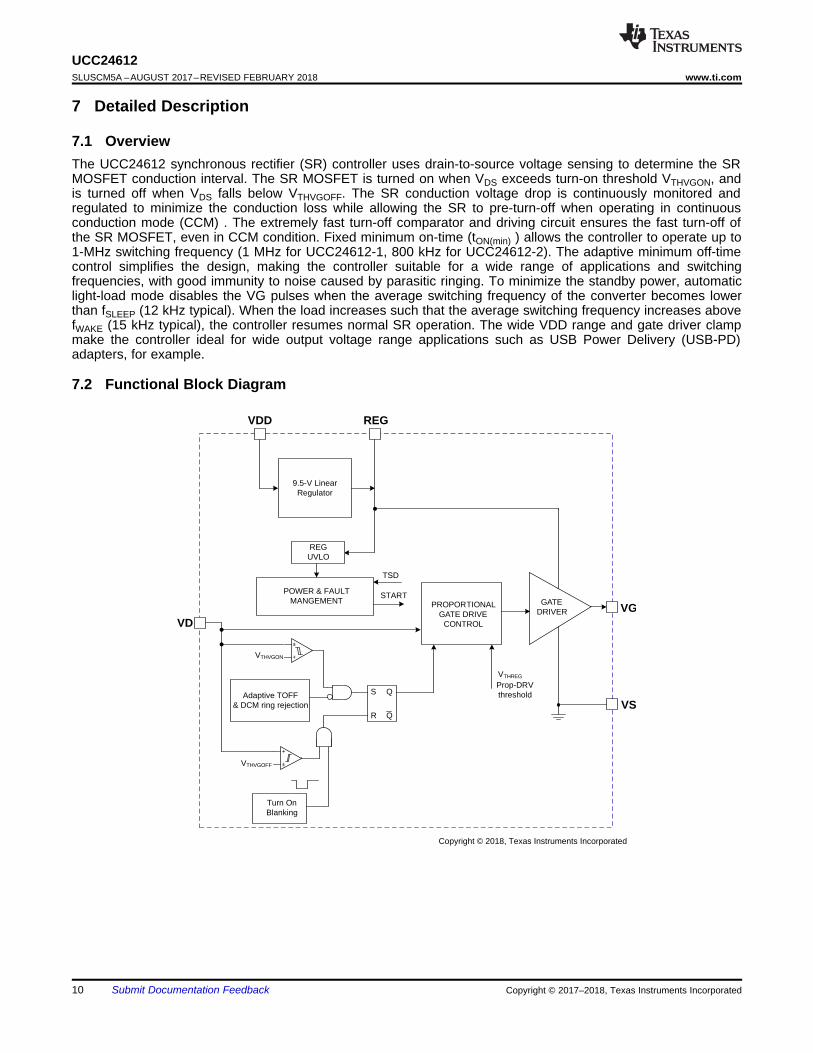
7.1 OverviewThe UCC24612 synchronous rectifier (SR) controller uses drain-to-source voltage sensing to determine the SRMOSFET conduction interval. The SR MOSFET is turned on when VDS exceeds turn-on threshold VTHVGON, andis turned off when VDS falls below VTHVGOFF. The SR conduction voltage drop is continuously monitored andregulated to minimize the conduction loss while allowing the SR to pre-turn-off when operating in continuousconduction mode (CCM) . The extremely fast turn-off comparator and driving circuit ensures the fast turn-off ofthe SR MOSFET, even in CCM condition. Fixed minimum on-time (tON(min) ) allows the controller to operate up to1-MHz switching frequency (1 MHz for UCC24612-1, 800 kHz for UCC24612-2). The adaptive minimum off-timecontrol simplifies the design, making the controller suitable for a wide range of applications and switchingfrequencies, with good immunity to noise caused by parasitic ringing. To minimize the standby power, automaticlight-load mode disables the VG pulses when the average switching frequency of the converter becomes lowerthan fSLEEP (12 kHz typical). When the load increases such that the average switching frequency increases abovefWAKE (15 kHz typical), the controller resumes normal SR operation. The wide VDD range and gate driver clampmake the controller ideal for wide output voltage range applications such as USB Power Delivery (USB-PD)adapters, for example.
7.2 Functional Block Diagram
VDD
VG VSVD
REG
11
UCC24612www.ti.com SLUSCM5A –AUGUST 2017–REVISED FEBRUARY 2018
Submit Documentation FeedbackCopyright © 2017–2018, Texas Instruments Incorporated
7.3 Feature Description
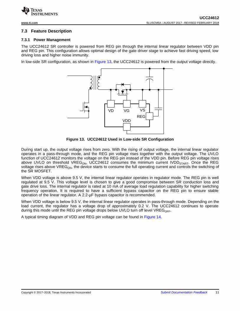
7.3.1 Power ManagementThe UCC24612 SR controller is powered from REG pin through the internal linear regulator between VDD pinand REG pin. This configuration allows optimal design of the gate driver stage to achieve fast driving speed, lowdriving loss and higher noise immunity.
In low-side SR configuration, as shown in Figure 13, the UCC24612 is powered from the output voltage directly.
Figure 13. UCC24612 Used in Low-side SR Configuration
During start up, the output voltage rises from zero. With the rising of output voltage, the internal linear regulatoroperates in a pass-through mode, and the REG pin voltage rises together with the output voltage. The UVLOfunction of UCC24612 monitors the voltage on the REG pin instead of the VDD pin. Before REG pin voltage risesabove UVLO on threshold VREGON, UCC24612 consumes the minimum current IVDDSTART. Once the REGvoltage rises above VREGON, the device starts to consume the full operating current and controls the switching ofthe SR MOSFET.
When VDD voltage is above 9.5 V, the internal linear regulator operates in regulator mode. The REG pin is wellregulated at 9.5 V. This voltage level is chosen to give a good compromise between SR conduction loss andgate drive loss. The internal regulator is rated at 10 mA of average load regulation capability for higher switchingfrequency operation. It is required to have a sufficient bypass capacitor on the REG pin to ensure stableoperation of the linear regulator. A 2.2-µF bypass capacitor is recommended.
When VDD voltage is below 9.5 V, the internal linear regulator operates in pass-through mode. Depending on theload current, the regulator has a voltage drop of approximately 0.2 V. The UCC24612 continues to operateduring this mode until the REG pin voltage drops below UVLO turn off level VREGOFF.
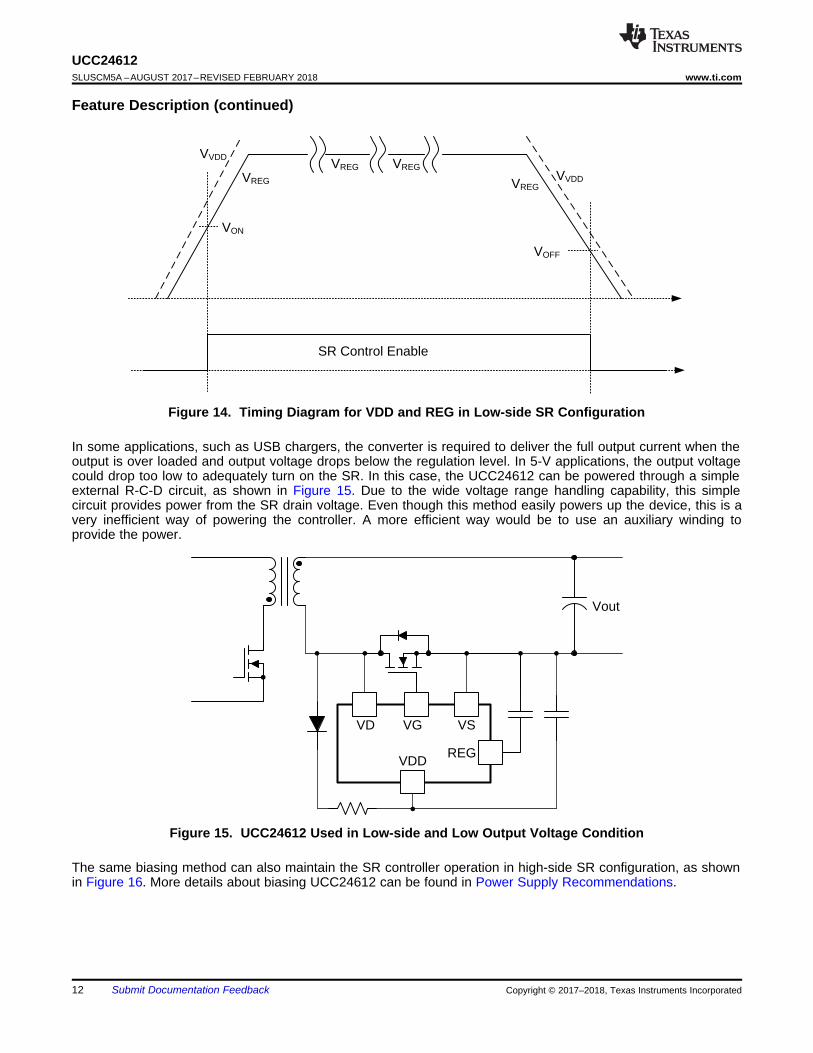
A typical timing diagram of VDD and REG pin voltage can be found in Figure 14.
Vout
VDD
VG VSVD
REG
VVDD
VREG VVDDVREG
VON
VOFF
SR Control Enable
VREGVREG
12
UCC24612SLUSCM5A –AUGUST 2017–REVISED FEBRUARY 2018 www.ti.com
Submit Documentation Feedback Copyright © 2017–2018, Texas Instruments Incorporated
Feature Description (continued)
Figure 14. Timing Diagram for VDD and REG in Low-side SR Configuration
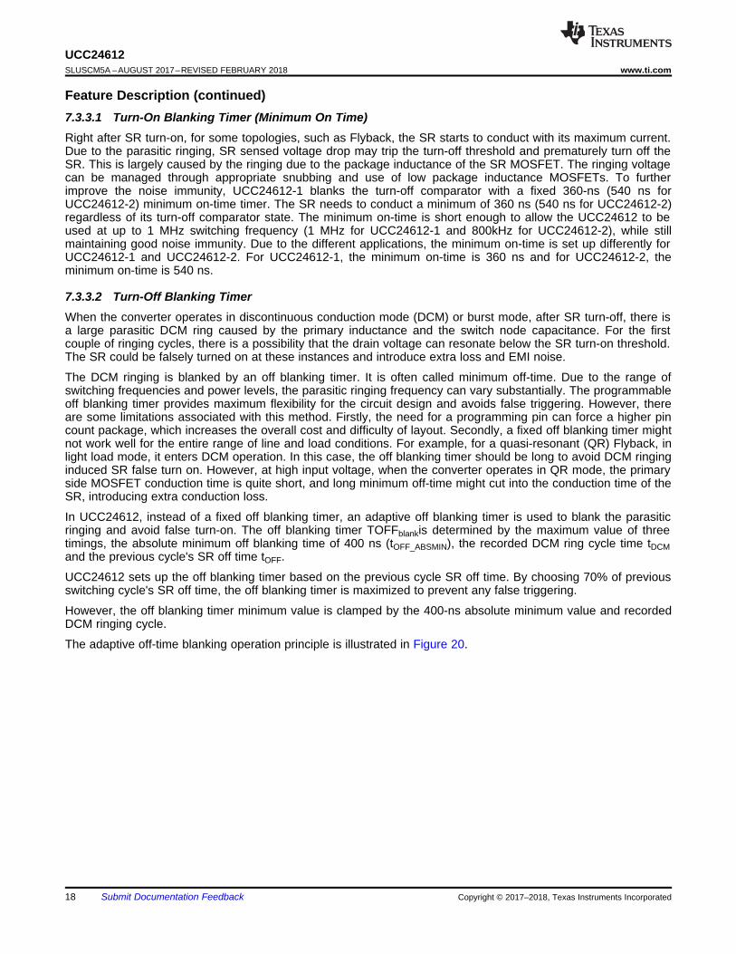
In some applications, such as USB chargers, the converter is required to deliver the full output current when theoutput is over loaded and output voltage drops below the regulation level. In 5-V applications, the output voltagecould drop too low to adequately turn on the SR. In this case, the UCC24612 can be powered through a simpleexternal R-C-D circuit, as shown in Figure 15. Due to the wide voltage range handling capability, this simplecircuit provides power from the SR drain voltage. Even though this method easily powers up the device, this is avery inefficient way of powering the controller. A more efficient way would be to use an auxiliary winding toprovide the power.
Figure 15. UCC24612 Used in Low-side and Low Output Voltage Condition
The same biasing method can also maintain the SR controller operation in high-side SR configuration, as shownin Figure 16. More details about biasing UCC24612 can be found in Power Supply Recommendations.

VDD
VGVS VD
REG
Vout
13
UCC24612www.ti.com SLUSCM5A –AUGUST 2017–REVISED FEBRUARY 2018
Submit Documentation FeedbackCopyright © 2017–2018, Texas Instruments Incorporated
Feature Description (continued)
Figure 16. UCC24612 Used in High-Side SR Configuration
7.3.2 Synchronous Rectifier ControlThe UCC24612 SR controller determines the conduction time of the SR-MOSFET by comparing the drain-to-source voltage (Vds) of the MOSFET against a turn-on threshold and a turn-off threshold. The VG output isdriven high when VDS of the MOSFET falls below VTHVGON and is driven low when VDS rises above VTHVGOFF asillustrated in Figure 17. Since when SR is conducting, its drain to source voltage (VDS) is negative, more negativevoltage drop means higher SR current.

VTHVGON
VTHREG
VTHVGOFF
10%
90%
tdVGON
tr_VG
ISD
VDS
VGATE
t
t
14
UCC24612SLUSCM5A –AUGUST 2017–REVISED FEBRUARY 2018 www.ti.com
Submit Documentation Feedback Copyright © 2017–2018, Texas Instruments Incorporated
Feature Description (continued)
Figure 17. VG Output With Respect to VDS
NOTEBecause of finite propagation delay and rise times, the body diode of the SR-MOSFETmay conduct briefly after VTHVGON has been exceeded. A waveform similar to that depictedin Figure 17 can be observed during SR operation in a simple Flyback circuit.
It should be noted that before the SR turns on, there is a small delay caused by the internal comparator delayand the gate driver delay. During the delay time, the SR MOSFET body diode is conducting. For a Flybackconverter, the SR current is at its maximum value during this delay time. It is desirable to have minimum delay.The gate driver design should avoid long turn-on delay.
For certain applications, this delay is essential for correct operation. In Active Clamp Flyback converters,especially when the primary-side switches are using Si-based super-junction MOSFETs, due to the largenonlinear junction capacitance, the SR often sees a leading spike current, followed by the real conductioncurrent. Typically, a longer minimum on-time can override this spike to make the circuit operate normally.However, this forced minimum on-time can allow current that transfers the energy from output to input andreduces the overall converter efficiency. In UCC24612, two different versions are available. UCC24612-1 has aninherently short turn-on propagation delay (80 ns typical) and can be used with the converters that need shorterdelay, such as standard Flyback converters or Active Clamp Flyback converters using GaN MOSFETs as mainswitches. UCC24612-2 has a longer 170-ns turn-on delay, to further ignore the leading edge spike and can beused with Active Clamp Flyback using Si-based super-junction MOSFETs as the main switch or LLC converters.Due to the longer turn-on delay, UCC24612-2 also increases its minimum on time-to 540ns to allow furtherenhancement on dealing with resonant-shape current, which makes a better choice for Si-based super-junctionMOSFETs as the main switch or LLC converters.

15
UCC24612www.ti.com SLUSCM5A –AUGUST 2017–REVISED FEBRUARY 2018
Submit Documentation FeedbackCopyright © 2017–2018, Texas Instruments Incorporated
Feature Description (continued)When the SR body diode is conducting, the VD pin becomes negative with respect to the VS pin, by a body-diode drop. The connections of VD and VS pins should be tracked directly to the SR MOSFET pins, to avoid anyoverlap of sensing and power paths, minimizing the negative voltage and ringing caused by the parasiticinductances. Low package inductance MOSFETs are preferred to minimize this effect.
Besides the simple comparator, UCC24612 also includes a proportional gate driver for the SR. For conventionalSR control, the SR MOSFET is always driven to the full driving voltage. This minimizes the conduction loss.However, this method has some major drawbacks. The turn-off threshold is often a fixed value, to prevent shoot-through, so that the SR is turned off before its current reaches zero. This causes SR body diode conduction andactually increases the conduction loss. Another issue is associated with operation in continuous conduction mode(CCM) condition. When a Flyback converter operates in CCM, the SR current slope (di/dt) at turn-off could be ashigh as 150 A/µs. This high current slope could cause large negative current due to long propagation delay.Furthermore, the delay caused by discharging the SR MOSFET gate from full voltage to its threshold levelintroduces another delay, further increasing the negative current.
Instead of keeping the SR MOSFET turned on with full gate driver voltage, UCC24612 reduces its gate drivervoltage when the voltage drop across SR drain-to-source reaches -50 mV (current approaching zero). During thistime, UCC24612 tries to regulate the SR voltage drop to -50 mV. This brings two major benefits to theapplication: a) Preventing the SR premature turn-off, avoiding extra loss associated with body diode conductionand reverse recovery, b) Shorter turn-off delay since the SR MOSFET gate voltage is already reduced close tothe threshold level and the SR can be turned off with virtually no further delay. Since the -150 mV is themaximum level that can be achieved by the UCC24612, the SR MOSFET selection should allow the -150-mVthreshold to be activated when operating in deep CCM condition.
In certain applications, such as telecom DC/DC bricks, due to the lower input and output voltages, operation indeep CCM mode (low inductor current ripple) gives the benefit of less conduction loss. In these applications, theSR turn-off current is high and the SR MOSFET voltage drop can still be less than the -50-mV threshold.UCC24612 decreases the -50-mV threshold to -150 mV to force proportional drive activation and reduction of thegate driver voltage for a fast turn-off. The timing to decrease the threshold is based on previous cycle SRconduction time. Because the regular proportional gate drive and the turn-off mechanism are kept functionalcontinuously, the UCC24612 can still provide correct SR control even for a large SR conduction time changewithin two switching cycles. The forced proportional gate drive mechanism can be shown in Figure 18. InFigure 18, the turn on delay was ignored to simplify the illustration.

-50mV
-150mV
90%TSR(N-1)
TSR(N)
90%TSR(N)
TSR(N+1)
ISR
VDS
VGATE
t
t
t
16
UCC24612SLUSCM5A –AUGUST 2017–REVISED FEBRUARY 2018 www.ti.com
Submit Documentation Feedback Copyright © 2017–2018, Texas Instruments Incorporated
Feature Description (continued)
Figure 18. Forced Proportional Gate-Drive for Deep CCM Operation
For Flyback converters, the SR current starts from its maximum amplitude and keeps reducing. Proportional gatedrive is only enabled at the later part of the SR current conduction period. However, for other topologies such asLLC or Active Clamp Flyback, the SR current starts from lower amplitude and then increases to a higheramplitude. To prevent the proportional gate drive from being enabled at the beginning of the conduction period,proportional drive is disabled for the first 50% of the SR conduction time, based on the previous cycle SRconduction time. In this way, the proportional drive is always enabled on the current falling slope and minimizesimpact on the conduction loss.

~~ ~~ ~~ ~~ ~~ ~~
ISD
VDS
TONBLANK
TOFFBLANK
SR Gate
17
UCC24612www.ti.com SLUSCM5A –AUGUST 2017–REVISED FEBRUARY 2018
Submit Documentation FeedbackCopyright © 2017–2018, Texas Instruments Incorporated
Feature Description (continued)7.3.3 Adaptive Blanking TimeIn power converters, the sensed the voltage across the SR is often noisy, caused by the parasitic ringing. Thisparasitic ringing is often associated with the SR and the primary-side switch turning on and off. Blanking time isused to deal with the parasitic ringing to prevent SR false turn on and off. Figure 19 shows more realisticwaveforms and the internal control timing which accommodates them.
Figure 19. Parasitic Ringing Associated with DCM Operation
18
UCC24612SLUSCM5A –AUGUST 2017–REVISED FEBRUARY 2018 www.ti.com
Submit Documentation Feedback Copyright © 2017–2018, Texas Instruments Incorporated
Feature Description (continued)7.3.3.1 Turn-On Blanking Timer (Minimum On Time)Right after SR turn-on, for some topologies, such as Flyback, the SR starts to conduct with its maximum current.Due to the parasitic ringing, SR sensed voltage drop may trip the turn-off threshold and prematurely turn off theSR. This is largely caused by the ringing due to the package inductance of the SR MOSFET. The ringing voltagecan be managed through appropriate snubbing and use of low package inductance MOSFETs. To furtherimprove the noise immunity, UCC24612-1 blanks the turn-off comparator with a fixed 360-ns (540 ns forUCC24612-2) minimum on-time timer. The SR needs to conduct a minimum of 360 ns (540 ns for UCC24612-2)regardless of its turn-off comparator state. The minimum on-time is short enough to allow the UCC24612 to beused at up to 1 MHz switching frequency (1 MHz for UCC24612-1 and 800kHz for UCC24612-2), while stillmaintaining good noise immunity. Due to the different applications, the minimum on-time is set up differently forUCC24612-1 and UCC24612-2. For UCC24612-1, the minimum on-time is 360 ns and for UCC24612-2, theminimum on-time is 540 ns.
7.3.3.2 Turn-Off Blanking TimerWhen the converter operates in discontinuous conduction mode (DCM) or burst mode, after SR turn-off, there isa large parasitic DCM ring caused by the primary inductance and the switch node capacitance. For the firstcouple of ringing cycles, there is a possibility that the drain voltage can resonate below the SR turn-on threshold.The SR could be falsely turned on at these instances and introduce extra loss and EMI noise.
The DCM ringing is blanked by an off blanking timer. It is often called minimum off-time. Due to the range ofswitching frequencies and power levels, the parasitic ringing frequency can vary substantially. The programmableoff blanking timer provides maximum flexibility for the circuit design and avoids false triggering. However, thereare some limitations associated with this method. Firstly, the need for a programming pin can force a higher pincount package, which increases the overall cost and difficulty of layout. Secondly, a fixed off blanking timer mightnot work well for the entire range of line and load conditions. For example, for a quasi-resonant (QR) Flyback, inlight load mode, it enters DCM operation. In this case, the off blanking timer should be long to avoid DCM ringinginduced SR false turn on. However, at high input voltage, when the converter operates in QR mode, the primaryside MOSFET conduction time is quite short, and long minimum off-time might cut into the conduction time of theSR, introducing extra conduction loss.
In UCC24612, instead of a fixed off blanking timer, an adaptive off blanking timer is used to blank the parasiticringing and avoid false turn-on. The off blanking timer TOFFblankis determined by the maximum value of threetimings, the absolute minimum off blanking time of 400 ns (tOFF_ABSMIN), the recorded DCM ring cycle time tDCMand the previous cycle's SR off time tOFF.
UCC24612 sets up the off blanking timer based on the previous cycle SR off time. By choosing 70% of previousswitching cycle's SR off time, the off blanking timer is maximized to prevent any false triggering.
However, the off blanking timer minimum value is clamped by the 400-ns absolute minimum value and recordedDCM ringing cycle.
The adaptive off-time blanking operation principle is illustrated in Figure 20.

C� C� C� C� C� C� C� C� C� C� C�C� C�
ISD
VDS
VGS
TOFF
Abs. Min TOFFBLANK
TOFFBLANK
TOFF(N-1) TOFF(N)
70%*TOFF(N-1)70%*TOFF(N-2)
19
UCC24612www.ti.com SLUSCM5A –AUGUST 2017–REVISED FEBRUARY 2018
Submit Documentation FeedbackCopyright © 2017–2018, Texas Instruments Incorporated
Feature Description (continued)
Figure 20. Operation Principle of Adaptive off-blanking
After SR turn-off, if the off blanking time is not sufficient, the SR could be turned on again by a DCM ring.Because of the DCM ring, the SR conduction time is limited by its minimum on-time. By looking at the SRconduction time and comparing it with the minimum on time, UCC24612 is able to determine if the conduction isa real SR conduction or a false turn on triggered by the DCM ring. A real SR conduction should demand theconduction time longer than the minimum on-time. Once the false turn-on is captured, the time duration betweenprevious SR turn-off and the SR false turn-on is recorded as the DCM ring cycle. For the next switching cycle,the off blanking timer is clamped to 2.2 times of the recorded DCM ring cycle. This clamp replaces the 350-nsclamp as the new minimum clamp for the adaptive-off blanking. This adaptive off-blanking timer allowsUCC24612 achieving the noise immunity without a dedicated programming pin. The DCM ring clamp is illustratedin Figure 21.

~~ ~~ ~~ ~~ ~~ ~~
ISD
VDS
SR ON
TOFFBLANK
ClampAbs. Min
TRing 2.2TRing
20
UCC24612SLUSCM5A –AUGUST 2017–REVISED FEBRUARY 2018 www.ti.com
Submit Documentation Feedback Copyright © 2017–2018, Texas Instruments Incorporated
Feature Description (continued)
Figure 21. Adaptive Off-Time Blanking with DCM Ring Clamp
For some conditions, as mentioned earlier, the off blanking timer suitable for DCM operation might be too longfor high-line QR operation. In this case, the off blanking timer clamp needs to be reset to the correct value.UCC24612 continuously monitors the SR body diode conduction time during minimum off-time. If the body diodeconduction time is longer than the minimum on-time, this means the minimum off blanking time clamp setting istoo long and needs to be reduced. UCC24612 resets the minimum off blanking time clamp to the absoluteminimum of 400 ns to allow full conduction of the SR on the subsequent cycles.
If for any reason the off blanking time expires after the SR body diode conduction, the SR turn-on is skipped forthe switching cycle. This is because when the SR conducts, it conducts with a minimum on-time, if the blankingtime expires at the end of the SR conduction time and converter operates in the CCM condition, there is a goodchance to cause shoot-through and endanger the converter.
The off blanking time has a maximum value of tOFF_MAX at 3.68 µs.

21
UCC24612www.ti.com SLUSCM5A –AUGUST 2017–REVISED FEBRUARY 2018
Submit Documentation FeedbackCopyright © 2017–2018, Texas Instruments Incorporated
Feature Description (continued)7.3.3.3 SR Turn-on Re-armThe VG output may only turn on when the controller has been armed for the next switching cycle. The controlleris armed for each successive SR cycle only after TOFFBLANK expires. The TOFFBLANK timer only starts after VDpin voltage rises 500 mV above the VS pin.
7.3.4 Gate Voltage ClampingWith the wide VDD voltage range capability, UCC24612 clamps the gate driver voltage to a maximum level of 9.5V to allow fast driving speed, low driving loss and compatibility with different MOSFETs. The 9.5-V level ischosen to minimize the conduction loss for the non-logic level MOSFETs.
The gate driver voltage clamp is achieved through the regulated REG pin voltage. When VDD voltage is above9.5 V, the linear regulator regulates the REG pin voltage to be 9.5 V, which is also the power supply of the gatedriver stage. This way, the MOSFET gate is clamped at 9.5 V, regardless of how high the VDD voltage is. Whenthe VDD voltage is close to or below the programmed REG pin regulation voltage, UCC24612 can no longerregulate the REG pin voltage. Instead, it enters a pass-through mode where the REG pin voltage follows theVDD pin voltage with slight voltage drop out (VREGDO). During this time, the gate driver voltage is lower than itsprogrammed value but still provides SR driving capability. The UCC24612 is disabled once the REG pin voltagedrops below its UVLO level.
7.3.5 Standby ModeWith more stringent efficiency standards such as Department of Energy (DoE) level VI, external power suppliesare expected to maintain very low standby power at no-load conditions. It is essential for the SR controller toenter the low-power standby mode to help save standby power.
During standby mode, the power converter loss allocation is quite different compared to heavy load. At heavierload, both conduction loss and switching loss are quite high. However, at light load, the conduction loss becomesinsignificant and switching loss dominates. To help improve standby power, modern power supply controllersoften enter burst mode to save switching loss. Furthermore, in each burst switching cycle, the energy delivered ismaximized to minimize the number of switching cycles needed and further reduce the switching loss.
Traditionally, the SR controller monitors the SR conduction time to distinguish normal operating modes fromstandby mode. This criterion is no longer suitable for the modern power supply controller designed for deliveringminimum standby power.
Instead, in UCC24612, a frequency based standby mode detection is used. UCC24612 continuously monitors theaverage switching frequency of the SR. Once the average switching frequency of the SR controller drops below12 kHz, the UCC24612 enters standby mode and reduces its current consumption to IVDDSTBY. During standbymode, the VG pin is kept low while the SR switching cycle is continuously monitored. Once the averageswitching frequency is more than 15 kHz over a 4.5-ms window, the SR operation is enabled again. UCC24612ignores the first six SR switching cycles after coming out of standby mode to make sure the SR isn't turned on inthe middle of the switching cycle.
22
UCC24612SLUSCM5A –AUGUST 2017–REVISED FEBRUARY 2018 www.ti.com
Submit Documentation Feedback Copyright © 2017–2018, Texas Instruments Incorporated
7.4 Device Functional Modes
7.4.1 UVLO ModeUCC24612 uses the REG pin voltage to detect UVLO instead of the VDD pin voltage. When the REG voltage tothe device has not yet reached the VREGON threshold, or has fallen below the UVLO threshold VREGOFF, thedevice operates in the low-power UVLO mode. In this mode, most internal functions are disabled and VDDcurrent is IVDDstart, typically less than 120 µA. If the REG pin is above 2 V, there is an active pull-down from VGto VS to prevent SR turn-on due to noise. When the REG pin voltage is less than 2 V, there is a weak pull downfrom VG to VS and this also helps prevent false turn on of the SR MOSFET. The device exits UVLO mode whenREG increases above the VREGON threshold.
7.4.2 Standby ModeStandby mode is a low-power operating mode to help achieve low standby power for the entire power supply.UCC24612 detects the operating frequency of the SR MOSFET and enters or exits standby mode operationautomatically. REG current reduces to IVDDSTBY level. During standby mode, the majority of the SR controlfunctions are disabled, except the switching frequency monitoring, REG monitoring and the active pull-down onthe gate driver.
7.4.3 Run ModeRun mode is the normal operating mode of the controller when not in UVLO mode or standby mode. In thismode, REG current is higher because all internal control and timing functions are operating and the VG output isdriving the MOSFET for synchronous rectification. REG current is the sum of IVDDRUN plus the average currentnecessary to drive the load on the VG output. The VG voltage is automatically adjusted based on the SRMOSFET drain to source voltage according to the proportional gate drive operation.

Copyright © 2018, Texas Instruments Incorporated
VIN
COUT
R1
R3 C3
Q1
5 1 2
VSVGVD
TP2 TP1
3 4
REG VDD
C1 C2
R2
VOUT
D1
TP3
D2
JP1
Closed
R4
UCC24612EVM
UCC24612U1
2.2
20k27V
10
1u2.2u
Note R3 and C3 are not Populated
1 2
J1
NP NS
T1
23
UCC24612www.ti.com SLUSCM5A –AUGUST 2017–REVISED FEBRUARY 2018
Submit Documentation FeedbackCopyright © 2017–2018, Texas Instruments Incorporated
8 Application and Implementation
NOTEInformation in the following application sections is not part of the TI componentspecification, and TI does not warrant its accuracy or completeness. TI’s customers areresponsible for determining suitability of components for their purposes. Customers shouldvalidate and test their design implementation to confirm system functionality.
8.1 Application InformationThe UCC24612 synchronous rectifier controller is designed to control an SR MOSFET to replace a lossy dioderectifier to improve the efficiency in various topologies, such as Active Clamp Flyback, Flyback operating in DCM,QR or CCM mode, as well as LLC resonant converters.
8.2 Typical ApplicationThe following application information is applied to the UCC24612 Evaluation Module (EVM), which is used as arectifier stage in a 20-V, 60-W DCM Flyback design. The controller used in this design is a UCC28740 secondaryside regulated, variable-frequency Flyback controller that has a maximum switching frequency of 85 kHz. Pleaserefer to the UCC28740 data sheet for further details.
Figure 22. UCC24612 Typical Application Example

� � VVV
VN
VVds OUT
PS
IN 127205.3
26522max max �
u �
:|! mA
mVRdson 7
2/14
50
24
UCC24612SLUSCM5A –AUGUST 2017–REVISED FEBRUARY 2018 www.ti.com
Submit Documentation Feedback Copyright © 2017–2018, Texas Instruments Incorporated
Typical Application (continued)8.2.1 Design Requirements
Table 2. 60-W DCM Flyback Design RequirementsPARAMETER TEST CONDITIONS MIN NOM MAX UNIT
INPUT CHARACTERISTICSVIN Input voltage 85 265 VRMS
OUTPUT CHARACTERISTICSVOUT Output voltage, average VIN = 85 VRMS to 265 VRMS, IOUT = 0 A to 3 A 19 20 21 VIOUT Output current VIN = 85 VRMS to 265 VRMS 0 3 A
8.2.2 Detailed Design Procedure
8.2.2.1 SR MOSFET SelectionUCC24612 can be paired with an appropriate MOSFET to replace the diode rectifier on existing designs anddemonstrate significant conduction loss reduction. The SR MOSFET selection should consider the tradeoffbetween cost and performance. Lower on-state resistance gives lower conduction loss, while it reduces theefficiency at light load. Due to the unique implementation of proportional gate drive, the benefit of lower on-stateresistance is diminished. It is recommended to select the MOSFET on-state resistance so that the proportionalgate drive operates for less than 50% of the full load SR conduction time.
According to UCC28740 datasheet, for 3-A output DCM Flyback design, the secondary side peak current shouldbe about 14 A. To allow the proportional gate drive operating less than 50% of the SR conduction time, SRMOSFET Rdson should be more than 7 mΩ , according to .
(1)
The MOSFET breakdown voltage should be higher than the maximum voltage the SR MOSFET sees undermaximum input voltage. For this design, the transformer turns ratio is 3.5, the voltage stress on the SR can becalculated as in Equation 2.
(2)
In this EVM, a 150-V, 19-mΩ MOSFET is used to get a balance between the cost and performance.
8.2.2.2 Bypass Capacitor SelectionUCC24612 needs a sufficient external bypass capacitance to ensure the internal regulator stability. Referring tothe power supply recommendation section, a 2.2-µF 50-V ceramic capacitor was chosen as the bypass capacitoron REG pin. For the VDD pin, it is normally powered by the output voltage and there is plenty of capacitor there.A 0.1-µF ceramic capacitor is still recommended to be placed close to the IC to provide high frequency current.
8.2.2.3 Snubber designIt is required for the user to setup snubber components C3 and R3 to get the best performance when using theUCC24612EVM.
To setup these components will require knowledge of the Flyback transformer secondary leakage inductance(Lslk) and measuring the secondary resonant ring frequency (fr) in circuit. It is recommended that the SR is notdriven while doing this to simplify the process. It is also recommended to do this test at partial load to avoidcreating too much heat on the SR body diode because the conduction loss is much higher. TP3 should bedisconnected from the Flyback converter to ensure FET Q1 is turned off while setting up the snubber.
The secondary winding capacitance (Cs) then needs to be calculated based on the following equation. Pleasenote for a transformer with a secondary winding leakage inductance of 3.8 µH and a ring frequency of 2 MHz, theparasitic capacitance would be 1.7 nF, for example.

COUT
R3 C3
Q1
5 1 2
VSVGVD
TP2 TP1
3 4
REG VDD
C1 C2
R2
VOUT
D1, 27V
TP3
D2
JP1
Open
R4
UCC24612EVM
UCC24612U1
2.2
20k
10
1u2.2u
Note: R3 and C3 are not Populated
J1
12
VIN
NP NS
IP
T1
R1
pFkHzRfsw
C 49747855
01.0
35
01.03 |
:uu
uu
:| 477.1
8.3
1
113
nF
H
Cs
Lslk
QR
P
� � � �nF
HMHzLslkfC
r
S 7.18.322
1
2
122 uuu
uuu
PSS
25
UCC24612www.ti.com SLUSCM5A –AUGUST 2017–REVISED FEBRUARY 2018
Submit Documentation FeedbackCopyright © 2017–2018, Texas Instruments Incorporated
(3)
Based on the calculated Cs, Lslk and fr, the snubber resistor R3 can be set to critically dampen the ringing onthe secondary, which requires setting the Q of the circuit equal to 1.
(4)
Capacitor C3 is used to limit the time the snubber resistor is applied to the aux winding during the switchingcycle. It is recommended to set the snubber capacitor C3 with the following equation based on the Flybackconverters switching frequency (fSW). For a Flyback converter switching at 85 kHz in the example would require aC3 of roughly 497 pF.
(5)
Please note that the calculations for R3 and C3 are just starting points and should be adjusted based onindividual preference, performance and efficiency requirements. More snubber design information can be foundin "Snubber Circuits Theory, Design and Application".
8.2.2.4 High-Side OperationTo use the UCC24612EVM to replace a high-side rectifier requires removing jumper JP1 and connecting theEVM as shown in Figure 23. Please note that the EVM comes with a default VDD filtering resistor (R2) of 20 kΩ.However, resistor R2 needs to be adjusted based on your individual application.
Figure 23. UCC24612-1EVM Used in High-Side Rectifier Application

88&&(/+0) = l8176 +8+0(/+0) ×0502
p×&/+0 = l208+728× 1
13p×0.36 = 9.28
88&&(/#:) = @8176 +8+0(/#:)× 05
02
A×&/#: = @208+3758× 1
13A×0.5 = 24.48
:|
uu
uu
! 187
10085
12
1
10012
12
kHzF
fswC
RPSS
26
UCC24612SLUSCM5A –AUGUST 2017–REVISED FEBRUARY 2018 www.ti.com
Submit Documentation Feedback Copyright © 2017–2018, Texas Instruments Incorporated
If the magnitude of the voltage from TP2 to TP1 is less than 28 V, remove R2 that is populated on the EVM ( 20kΩ) and set R2 to 0 to 10 ohms and remove 27-V Zener diode D1 from the board.
If TP2 to TP1 is greater than 28 V use resistor R2 to setup an averaging filter to lower the DC voltage applied toVDD.
The RC filter formed by C2 and R2 should set the filter pole frequency to one-hundredth of the converter'smaximum switching frequency. In this example the converter's maximum switching frequency (fSW) is 85 kHz.Note that the switching frequency will vary based on design and preference.
(6)
When the RC filter circuit is used, it is recommended that the VDD voltage should be between 4 V to 28 V toprovide enough energy and voltage to the gate driver. This range can be determined in a fixed frequency Flybackconverter with the following equations. DMAX is the maximum duty cycle of the converter and DMIN is the minimumduty cycle of the converter. NP is the Flyback transformer (T1) primary number of turns and NS is the transformersecondary number of turns. Please refer to Figure 23 for details.
Maximum VDD voltage (VVDD(MAX)):
(7)
Minimum VDD voltage (VVDD(MIN)):
(8)
8.2.3 Application CurvesThe UCC24612EVM is used as a synchronous rectifier in both a high-side and low-side configuration in an offline(VIN = 85 V to 265 V RMS), 20-V (VOUT), 60-W application. The primary-side controller used in this design is aUCC28740 secondary-side regulated, variable-frequency Flyback controller that had a maximum switchingfrequency of roughly 85 kHz. Please refer to the UCC28740 data sheet for further details.
8.2.3.1 Steady State Testing Low-Side Configuration• Snubber Components, R2 = 1.02 kΩ, R3 = 51.1Ω , C3 = 470 pF• CH1 = VG, CH2 = Q1 drain (TP2), CH3 = VOUT Voltage Ripple (TP3)
Figure 24. 85-VAC, 0-A Load Figure 25. 85-VAC, 3-A Load

27
UCC24612www.ti.com SLUSCM5A –AUGUST 2017–REVISED FEBRUARY 2018
Submit Documentation FeedbackCopyright © 2017–2018, Texas Instruments Incorporated
Figure 26. 265-VAC, 0-A Load Figure 27. 265-VAC, 3-A Load
28
UCC24612SLUSCM5A –AUGUST 2017–REVISED FEBRUARY 2018 www.ti.com
Submit Documentation Feedback Copyright © 2017–2018, Texas Instruments Incorporated
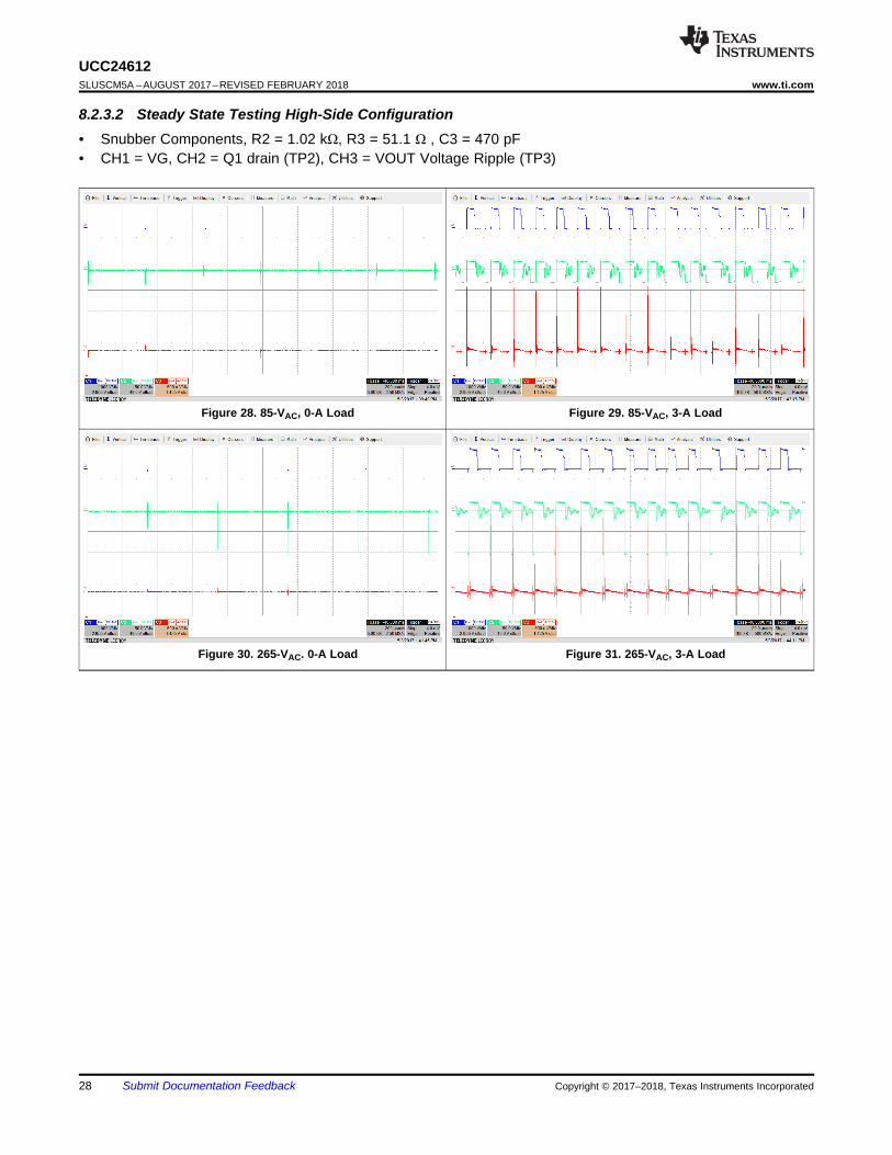
8.2.3.2 Steady State Testing High-Side Configuration• Snubber Components, R2 = 1.02 kΩ, R3 = 51.1 Ω , C3 = 470 pF• CH1 = VG, CH2 = Q1 drain (TP2), CH3 = VOUT Voltage Ripple (TP3)
Figure 28. 85-VAC, 0-A Load Figure 29. 85-VAC, 3-A Load
Figure 30. 265-VAC. 0-A Load Figure 31. 265-VAC, 3-A Load

VDD
VGVS VD
REG
Vout
29
UCC24612www.ti.com SLUSCM5A –AUGUST 2017–REVISED FEBRUARY 2018
Submit Documentation FeedbackCopyright © 2017–2018, Texas Instruments Incorporated
9 Power Supply RecommendationsUCC24612 internal circuits are powered from the REG pin only. There is an internal LDO between VDD pin andREG pin to provide a well-regulated REG pin voltage when VDD voltage is above 9.5 V. This allows the deviceto have better bypassing and better gate driver performance.
It is important to have sufficient bypass cap on REG pin. A minimum of 1.5-µF bypass capacitor is required.When the average gate charge current is higher than 5mA, it is required to have at least 2.2-µF bypass capacitoron REG pin.
VDD pin is the main power source of the device. The voltage on VDD pin should be kept between 4.5 V and 28V for normal operation. Refer to the electrical characteristics table for the tolerances on the REG pin UVLO ONand OFF levels.
When UCC24612 is used in low-side SR configuration, VDD can be directly tied to the output voltage if theoutput voltage is between 4.5 V to 28 V.
When the UCC24612 is used in high-side SR configuration, VDD can be powered through three different ways,with a trade off between cost and performance.a. Power the device through secondary-side auxiliary windingb. Power the device through simple R-C filterc. Power the device through depletion mode FET
By using the secondary-side auxiliary winding, as shown in Figure 32, UCC24612 is equivalently powered by theoutput voltage because of the transformer coupling effect. This provides the best efficiency solution. However,this solution is often limited by the transformer construction and cost constraints.
The UCC24612 can be powered by using a diode and RC filter on VDD pin, as shown in Figure 33. This allowsthe device to get power from the SR drain voltage. Due to the wide range of VD voltage variation (for example,VD voltage is the sum of reflected input voltage and output voltage in Flyback converter), this may not beacceptable for some applications due to the limit of absolute maximum VDD voltage rating. However, thisprovides a simple and low cost solution.
A more universal solution without changing the transformer is to provide the VDD through SR drain using a diodeand depletion mode MOSFET, as shown in Figure 34. This allows a well regulated VDD voltage throughout theentire operation range of the converter. Even though it still reducess the efficiency because the device ispowered up from a high voltage source, this provides a simple solution without changing the transformer design.
The three different configurations are summarized in Figure 32, Figure 33 and Figure 34.
Figure 32. Power UCC24612 Using Auxiliary Winding

VDD
VGVS VD
REG
Vout
VDD
VGVS VD
REG
Vout
30
UCC24612SLUSCM5A –AUGUST 2017–REVISED FEBRUARY 2018 www.ti.com
Submit Documentation Feedback Copyright © 2017–2018, Texas Instruments Incorporated
Figure 33. Power UCC24612 Using R-C-D
Figure 34. Powering UCC24612 Using Depletion Mode MOSFET
UCC24612 CVDD
CREG
RG
SR MOSFET
VD
VD
D
VG VS
RE
G
SR Source
SR Drain
31
UCC24612www.ti.com SLUSCM5A –AUGUST 2017–REVISED FEBRUARY 2018
Submit Documentation FeedbackCopyright © 2017–2018, Texas Instruments Incorporated
10 PCB Layout
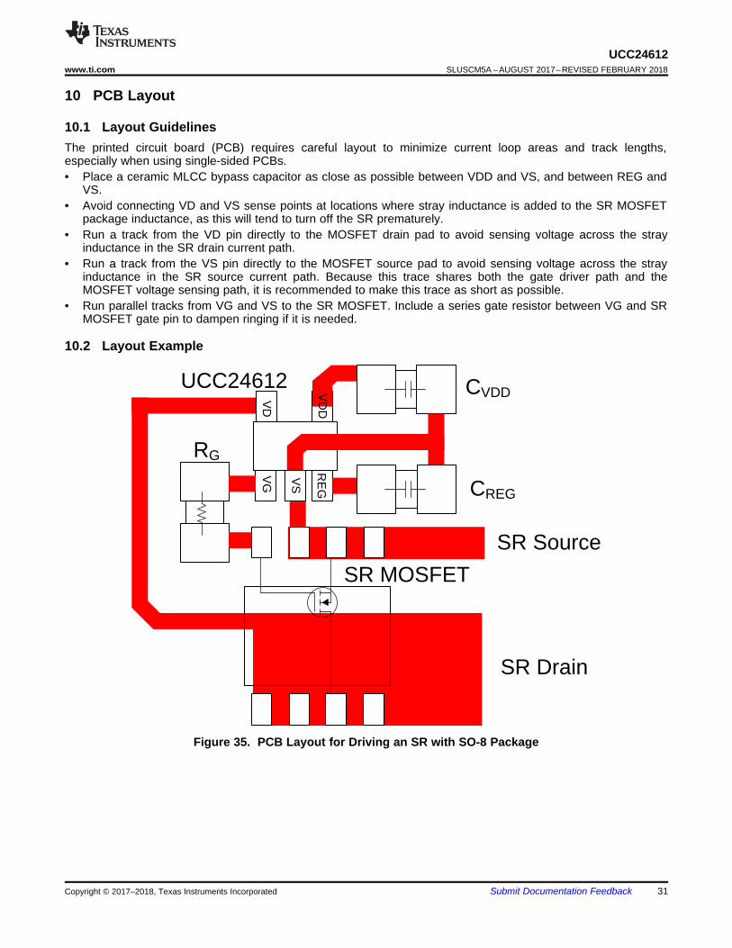
10.1 Layout GuidelinesThe printed circuit board (PCB) requires careful layout to minimize current loop areas and track lengths,especially when using single-sided PCBs.• Place a ceramic MLCC bypass capacitor as close as possible between VDD and VS, and between REG and
VS.• Avoid connecting VD and VS sense points at locations where stray inductance is added to the SR MOSFET
package inductance, as this will tend to turn off the SR prematurely.• Run a track from the VD pin directly to the MOSFET drain pad to avoid sensing voltage across the stray
inductance in the SR drain current path.• Run a track from the VS pin directly to the MOSFET source pad to avoid sensing voltage across the stray
inductance in the SR source current path. Because this trace shares both the gate driver path and theMOSFET voltage sensing path, it is recommended to make this trace as short as possible.
• Run parallel tracks from VG and VS to the SR MOSFET. Include a series gate resistor between VG and SRMOSFET gate pin to dampen ringing if it is needed.
10.2 Layout Example
Figure 35. PCB Layout for Driving an SR with SO-8 Package
32
UCC24612SLUSCM5A –AUGUST 2017–REVISED FEBRUARY 2018 www.ti.com
Submit Documentation Feedback Copyright © 2017–2018, Texas Instruments Incorporated
11 Device and Documentation Support
11.1 Community ResourcesThe following links connect to TI community resources. Linked contents are provided "AS IS" by the respectivecontributors. They do not constitute TI specifications and do not necessarily reflect TI's views; see TI's Terms ofUse.
TI E2E™ Online Community TI's Engineer-to-Engineer (E2E) Community. Created to foster collaborationamong engineers. At e2e.ti.com, you can ask questions, share knowledge, explore ideas and helpsolve problems with fellow engineers.
Design Support TI's Design Support Quickly find helpful E2E forums along with design support tools andcontact information for technical support.
11.2 TrademarksE2E is a trademark of Texas Instruments.
11.3 Electrostatic Discharge CautionThese devices have limited built-in ESD protection. The leads should be shorted together or the device placed in conductive foamduring storage or handling to prevent electrostatic damage to the MOS gates.
11.4 GlossarySLYZ022 — TI Glossary.
This glossary lists and explains terms, acronyms, and definitions.
12 Mechanical, Packaging, and Orderable InformationThe following pages include mechanical, packaging, and orderable information. This information is the mostcurrent data available for the designated devices. This data is subject to change without notice and revision ofthis document. For browser-based versions of this data sheet, refer to the left-hand navigation.
PACKAGE OPTION ADDENDUM
www.ti.com 21-Feb-2018
Addendum-Page 1
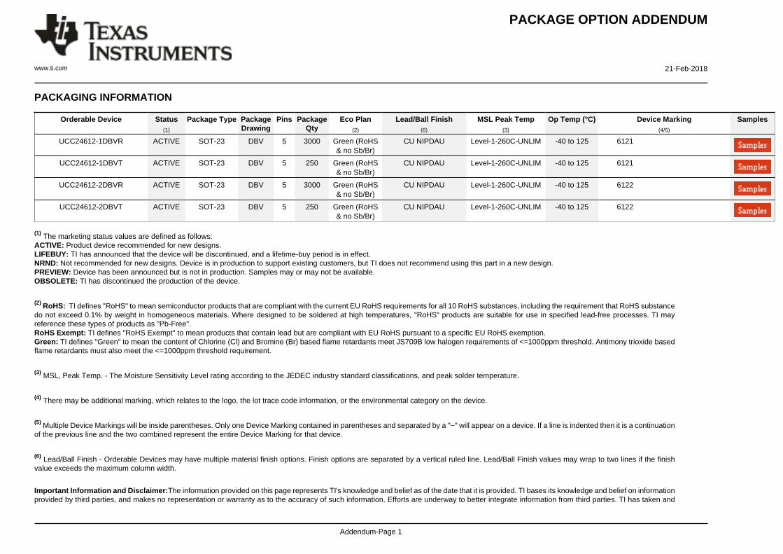
PACKAGING INFORMATION
Orderable Device Status(1)
Package Type PackageDrawing
Pins PackageQty
Eco Plan(2)
Lead/Ball Finish(6)
MSL Peak Temp(3)
Op Temp (°C) Device Marking(4/5)
Samples
UCC24612-1DBVR ACTIVE SOT-23 DBV 5 3000 Green (RoHS& no Sb/Br)
CU NIPDAU Level-1-260C-UNLIM -40 to 125 6121
UCC24612-1DBVT ACTIVE SOT-23 DBV 5 250 Green (RoHS& no Sb/Br)
CU NIPDAU Level-1-260C-UNLIM -40 to 125 6121
UCC24612-2DBVR ACTIVE SOT-23 DBV 5 3000 Green (RoHS& no Sb/Br)
CU NIPDAU Level-1-260C-UNLIM -40 to 125 6122
UCC24612-2DBVT ACTIVE SOT-23 DBV 5 250 Green (RoHS& no Sb/Br)
CU NIPDAU Level-1-260C-UNLIM -40 to 125 6122
(1) The marketing status values are defined as follows:ACTIVE: Product device recommended for new designs.LIFEBUY: TI has announced that the device will be discontinued, and a lifetime-buy period is in effect.NRND: Not recommended for new designs. Device is in production to support existing customers, but TI does not recommend using this part in a new design.PREVIEW: Device has been announced but is not in production. Samples may or may not be available.OBSOLETE: TI has discontinued the production of the device.
(2) RoHS: TI defines "RoHS" to mean semiconductor products that are compliant with the current EU RoHS requirements for all 10 RoHS substances, including the requirement that RoHS substancedo not exceed 0.1% by weight in homogeneous materials. Where designed to be soldered at high temperatures, "RoHS" products are suitable for use in specified lead-free processes. TI mayreference these types of products as "Pb-Free".RoHS Exempt: TI defines "RoHS Exempt" to mean products that contain lead but are compliant with EU RoHS pursuant to a specific EU RoHS exemption.Green: TI defines "Green" to mean the content of Chlorine (Cl) and Bromine (Br) based flame retardants meet JS709B low halogen requirements of <=1000ppm threshold. Antimony trioxide basedflame retardants must also meet the <=1000ppm threshold requirement.
(3) MSL, Peak Temp. - The Moisture Sensitivity Level rating according to the JEDEC industry standard classifications, and peak solder temperature.
(4) There may be additional marking, which relates to the logo, the lot trace code information, or the environmental category on the device.
(5) Multiple Device Markings will be inside parentheses. Only one Device Marking contained in parentheses and separated by a "~" will appear on a device. If a line is indented then it is a continuationof the previous line and the two combined represent the entire Device Marking for that device.
(6) Lead/Ball Finish - Orderable Devices may have multiple material finish options. Finish options are separated by a vertical ruled line. Lead/Ball Finish values may wrap to two lines if the finishvalue exceeds the maximum column width.
Important Information and Disclaimer:The information provided on this page represents TI's knowledge and belief as of the date that it is provided. TI bases its knowledge and belief on informationprovided by third parties, and makes no representation or warranty as to the accuracy of such information. Efforts are underway to better integrate information from third parties. TI has taken and
PACKAGE OPTION ADDENDUM
www.ti.com 21-Feb-2018
Addendum-Page 2
continues to take reasonable steps to provide representative and accurate information but may not have conducted destructive testing or chemical analysis on incoming materials and chemicals.TI and TI suppliers consider certain information to be proprietary, and thus CAS numbers and other limited information may not be available for release.
In no event shall TI's liability arising out of such information exceed the total purchase price of the TI part(s) at issue in this document sold by TI to Customer on an annual basis.

www.ti.com
PACKAGE OUTLINE
C
TYP0.220.08
0.25
3.02.6
2X 0.95
1.9
1.45 MAX
TYP0.150.00
5X 0.50.3
TYP0.60.3
TYP80
1.9
A
3.052.75
B1.751.45
(1.1)
SOT-23 - 1.45 mm max heightDBV0005ASMALL OUTLINE TRANSISTOR
4214839/C 04/2017
NOTES: 1. All linear dimensions are in millimeters. Any dimensions in parenthesis are for reference only. Dimensioning and tolerancing per ASME Y14.5M.2. This drawing is subject to change without notice.3. Refernce JEDEC MO-178.
0.2 C A B
1
34
5
2
INDEX AREAPIN 1
GAGE PLANE
SEATING PLANE
0.1 C
SCALE 4.000
www.ti.com
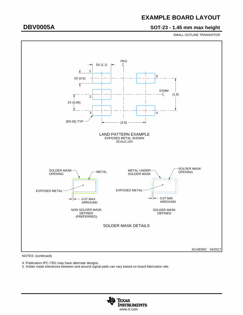
EXAMPLE BOARD LAYOUT
0.07 MAXARROUND
0.07 MINARROUND
5X (1.1)
5X (0.6)
(2.6)
(1.9)
2X (0.95)
(R0.05) TYP
4214839/C 04/2017
SOT-23 - 1.45 mm max heightDBV0005ASMALL OUTLINE TRANSISTOR
NOTES: (continued) 4. Publication IPC-7351 may have alternate designs. 5. Solder mask tolerances between and around signal pads can vary based on board fabrication site.
SYMM
LAND PATTERN EXAMPLEEXPOSED METAL SHOWN
SCALE:15X
PKG
1
3 4
5
2
SOLDER MASKOPENINGMETAL UNDER
SOLDER MASK
SOLDER MASKDEFINED
EXPOSED METAL
METALSOLDER MASKOPENING
NON SOLDER MASKDEFINED
(PREFERRED)
SOLDER MASK DETAILS
EXPOSED METAL
www.ti.com
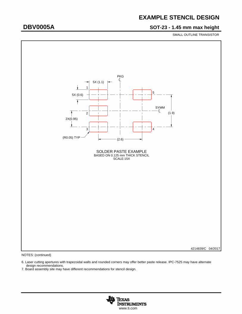
EXAMPLE STENCIL DESIGN
(2.6)
(1.9)
2X(0.95)
5X (1.1)
5X (0.6)
(R0.05) TYP
SOT-23 - 1.45 mm max heightDBV0005ASMALL OUTLINE TRANSISTOR
4214839/C 04/2017
NOTES: (continued) 6. Laser cutting apertures with trapezoidal walls and rounded corners may offer better paste release. IPC-7525 may have alternate design recommendations. 7. Board assembly site may have different recommendations for stencil design.
SOLDER PASTE EXAMPLEBASED ON 0.125 mm THICK STENCIL
SCALE:15X
SYMM
PKG
1
3 4
5
2

www.ti.com
PACKAGE OUTLINE
C
TYP0.220.08
0.25
3.02.6
2X 0.95
1.9
1.45 MAX
TYP0.150.00
5X 0.50.3
TYP0.60.3
TYP80
1.9
A
3.052.75
B1.751.45
(1.1)
SOT-23 - 1.45 mm max heightDBV0005ASMALL OUTLINE TRANSISTOR
4214839/C 04/2017
NOTES: 1. All linear dimensions are in millimeters. Any dimensions in parenthesis are for reference only. Dimensioning and tolerancing per ASME Y14.5M.2. This drawing is subject to change without notice.3. Refernce JEDEC MO-178.
0.2 C A B
1
34
5
2
INDEX AREAPIN 1
GAGE PLANE
SEATING PLANE
0.1 C
SCALE 4.000

www.ti.com
EXAMPLE BOARD LAYOUT
0.07 MAXARROUND
0.07 MINARROUND
5X (1.1)
5X (0.6)
(2.6)
(1.9)
2X (0.95)
(R0.05) TYP
4214839/C 04/2017
SOT-23 - 1.45 mm max heightDBV0005ASMALL OUTLINE TRANSISTOR
NOTES: (continued) 4. Publication IPC-7351 may have alternate designs. 5. Solder mask tolerances between and around signal pads can vary based on board fabrication site.
SYMM
LAND PATTERN EXAMPLEEXPOSED METAL SHOWN
SCALE:15X
PKG
1
3 4
5
2
SOLDER MASKOPENINGMETAL UNDER
SOLDER MASK
SOLDER MASKDEFINED
EXPOSED METAL
METALSOLDER MASKOPENING
NON SOLDER MASKDEFINED
(PREFERRED)
SOLDER MASK DETAILS
EXPOSED METAL

www.ti.com
EXAMPLE STENCIL DESIGN
(2.6)
(1.9)
2X(0.95)
5X (1.1)
5X (0.6)
(R0.05) TYP
SOT-23 - 1.45 mm max heightDBV0005ASMALL OUTLINE TRANSISTOR
4214839/C 04/2017
NOTES: (continued) 6. Laser cutting apertures with trapezoidal walls and rounded corners may offer better paste release. IPC-7525 may have alternate design recommendations. 7. Board assembly site may have different recommendations for stencil design.
SOLDER PASTE EXAMPLEBASED ON 0.125 mm THICK STENCIL
SCALE:15X
SYMM
PKG
1
3 4
5
2
IMPORTANT NOTICE
Texas Instruments Incorporated (TI) reserves the right to make corrections, enhancements, improvements and other changes to itssemiconductor products and services per JESD46, latest issue, and to discontinue any product or service per JESD48, latest issue. Buyersshould obtain the latest relevant information before placing orders and should verify that such information is current and complete.TI’s published terms of sale for semiconductor products (http://www.ti.com/sc/docs/stdterms.htm) apply to the sale of packaged integratedcircuit products that TI has qualified and released to market. Additional terms may apply to the use or sale of other types of TI products andservices.Reproduction of significant portions of TI information in TI data sheets is permissible only if reproduction is without alteration and isaccompanied by all associated warranties, conditions, limitations, and notices. TI is not responsible or liable for such reproduceddocumentation. Information of third parties may be subject to additional restrictions. Resale of TI products or services with statementsdifferent from or beyond the parameters stated by TI for that product or service voids all express and any implied warranties for theassociated TI product or service and is an unfair and deceptive business practice. TI is not responsible or liable for any such statements.Buyers and others who are developing systems that incorporate TI products (collectively, “Designers”) understand and agree that Designersremain responsible for using their independent analysis, evaluation and judgment in designing their applications and that Designers havefull and exclusive responsibility to assure the safety of Designers' applications and compliance of their applications (and of all TI productsused in or for Designers’ applications) with all applicable regulations, laws and other applicable requirements. Designer represents that, withrespect to their applications, Designer has all the necessary expertise to create and implement safeguards that (1) anticipate dangerousconsequences of failures, (2) monitor failures and their consequences, and (3) lessen the likelihood of failures that might cause harm andtake appropriate actions. Designer agrees that prior to using or distributing any applications that include TI products, Designer willthoroughly test such applications and the functionality of such TI products as used in such applications.TI’s provision of technical, application or other design advice, quality characterization, reliability data or other services or information,including, but not limited to, reference designs and materials relating to evaluation modules, (collectively, “TI Resources”) are intended toassist designers who are developing applications that incorporate TI products; by downloading, accessing or using TI Resources in anyway, Designer (individually or, if Designer is acting on behalf of a company, Designer’s company) agrees to use any particular TI Resourcesolely for this purpose and subject to the terms of this Notice.TI’s provision of TI Resources does not expand or otherwise alter TI’s applicable published warranties or warranty disclaimers for TIproducts, and no additional obligations or liabilities arise from TI providing such TI Resources. TI reserves the right to make corrections,enhancements, improvements and other changes to its TI Resources. TI has not conducted any testing other than that specificallydescribed in the published documentation for a particular TI Resource.Designer is authorized to use, copy and modify any individual TI Resource only in connection with the development of applications thatinclude the TI product(s) identified in such TI Resource. NO OTHER LICENSE, EXPRESS OR IMPLIED, BY ESTOPPEL OR OTHERWISETO ANY OTHER TI INTELLECTUAL PROPERTY RIGHT, AND NO LICENSE TO ANY TECHNOLOGY OR INTELLECTUAL PROPERTYRIGHT OF TI OR ANY THIRD PARTY IS GRANTED HEREIN, including but not limited to any patent right, copyright, mask work right, orother intellectual property right relating to any combination, machine, or process in which TI products or services are used. Informationregarding or referencing third-party products or services does not constitute a license to use such products or services, or a warranty orendorsement thereof. Use of TI Resources may require a license from a third party under the patents or other intellectual property of thethird party, or a license from TI under the patents or other intellectual property of TI.TI RESOURCES ARE PROVIDED “AS IS” AND WITH ALL FAULTS. TI DISCLAIMS ALL OTHER WARRANTIES ORREPRESENTATIONS, EXPRESS OR IMPLIED, REGARDING RESOURCES OR USE THEREOF, INCLUDING BUT NOT LIMITED TOACCURACY OR COMPLETENESS, TITLE, ANY EPIDEMIC FAILURE WARRANTY AND ANY IMPLIED WARRANTIES OFMERCHANTABILITY, FITNESS FOR A PARTICULAR PURPOSE, AND NON-INFRINGEMENT OF ANY THIRD PARTY INTELLECTUALPROPERTY RIGHTS. TI SHALL NOT BE LIABLE FOR AND SHALL NOT DEFEND OR INDEMNIFY DESIGNER AGAINST ANY CLAIM,INCLUDING BUT NOT LIMITED TO ANY INFRINGEMENT CLAIM THAT RELATES TO OR IS BASED ON ANY COMBINATION OFPRODUCTS EVEN IF DESCRIBED IN TI RESOURCES OR OTHERWISE. IN NO EVENT SHALL TI BE LIABLE FOR ANY ACTUAL,DIRECT, SPECIAL, COLLATERAL, INDIRECT, PUNITIVE, INCIDENTAL, CONSEQUENTIAL OR EXEMPLARY DAMAGES INCONNECTION WITH OR ARISING OUT OF TI RESOURCES OR USE THEREOF, AND REGARDLESS OF WHETHER TI HAS BEENADVISED OF THE POSSIBILITY OF SUCH DAMAGES.Unless TI has explicitly designated an individual product as meeting the requirements of a particular industry standard (e.g., ISO/TS 16949and ISO 26262), TI is not responsible for any failure to meet such industry standard requirements.Where TI specifically promotes products as facilitating functional safety or as compliant with industry functional safety standards, suchproducts are intended to help enable customers to design and create their own applications that meet applicable functional safety standardsand requirements. Using products in an application does not by itself establish any safety features in the application. Designers mustensure compliance with safety-related requirements and standards applicable to their applications. Designer may not use any TI products inlife-critical medical equipment unless authorized officers of the parties have executed a special contract specifically governing such use.Life-critical medical equipment is medical equipment where failure of such equipment would cause serious bodily injury or death (e.g., lifesupport, pacemakers, defibrillators, heart pumps, neurostimulators, and implantables). Such equipment includes, without limitation, allmedical devices identified by the U.S. Food and Drug Administration as Class III devices and equivalent classifications outside the U.S.TI may expressly designate certain products as completing a particular qualification (e.g., Q100, Military Grade, or Enhanced Product).Designers agree that it has the necessary expertise to select the product with the appropriate qualification designation for their applicationsand that proper product selection is at Designers’ own risk. Designers are solely responsible for compliance with all legal and regulatoryrequirements in connection with such selection.Designer will fully indemnify TI and its representatives against any damages, costs, losses, and/or liabilities arising out of Designer’s non-compliance with the terms and provisions of this Notice.
Mailing Address: Texas Instruments, Post Office Box 655303, Dallas, Texas 75265Copyright © 2018, Texas Instruments Incorporated