Embed Size (px)
Citation preview
LMV1099
www.ti.com SNAS490D –JULY 2010–REVISED MAY 2013
LMV1099 Uplink Far Field Noise Suppression and Downlink SNR Enhancing MicrophoneAmplifier with Earpiece Driver
Check for Samples: LMV1099
1FEATURES DESCRIPTIONThe LMV1099 is an uplink and downlink voice
2• Noise Reduction Without DSP-Type Artifactsintelligibility enhancing analog IC, ideally suited for
• Adapting AGC (Automatic Gain Control) on mobile handsets. Uplink voice intelligibility isAmbient Noise Level and Downlink Signal improved by rejecting far-field noise through a uniqueStrength two-microphone solution. Downlink voice intelligibility
is improved by enhancing the SNR (Signal-to-Noise• Downlink Adjustable Noise-reducing HighRatio) between the downlink voice and the ambientPass Filternoise environment at the user’s earpiece.• Separate Uplink and Downlink Enable
Functions The LMV1099 preserves uplink near-field voicesignals within close range of the microphones while• No Added Process Delaysrejecting far-field acoustic noise greater than 0.5m
• Low Power Consumption from the microphones.• Shutdown Function
The LMV1099 also enhances downlink voice• Maximum AGC Limiter intelligibility by improving near-field SNR based on• Differential Inputs and Outputs for Noise the user’s environment. The analog circuitry adapts
dynamically to both the user’s ambient noiseImmunityenvironment as well as the downlink signal amplitude• Earpiece Amplifierto ensure optimum SNRI (signal-to-noise ratio
• Available in a 25-Bump DSBGA Package improvement). The downlink path also provides uplinknoise attenuation through an adjustable high pass
APPLICATIONS filter before the SNR enhanced downlink voicereaches the user’s earpiece.• Mobile HandsetsUnlike digital-based noise reduction solutions, the all-• Mobile and Handheld Two-Way Radiosanalog low power consuming LMV1099 increases• Bluetooth and Other Power Headsetsboth uplink and downlink voice intelligibility withoutDSP-type artifacts, distortions or processing delays.KEY SPECIFICATIONS
• Uplink Far Field Noise Suppression (ElectricalFFNSE at f = 1kHz) 33dB (typ)
• Near-Field SNR Enhancement 6 to 18dB (typ)• Downlink SNRIE 16dB (typ)• Supply Voltage Range 2.7V to 5.5V• Supply Current (VDD = 3.6V) 3.8mA (typ)• Shutdown Current 0.06μA (typ)• Uplink PSRR (f = 217Hz) 106dB (typ)• Downlink SNR (A-weighted) 102dB (typ)• Downlink THD+N 0.03% (typ)• Earpiece Output Power (RL = 32Ω) 83mW (typ)
1
Please be aware that an important notice concerning availability, standard warranty, and use in critical applications ofTexas Instruments semiconductor products and disclaimers thereto appears at the end of this data sheet.
2All trademarks are the property of their respective owners.
PRODUCTION DATA information is current as of publication date. Copyright © 2010–2013, Texas Instruments IncorporatedProducts conform to specifications per the terms of the TexasInstruments standard warranty. Production processing does notnecessarily include testing of all parameters.
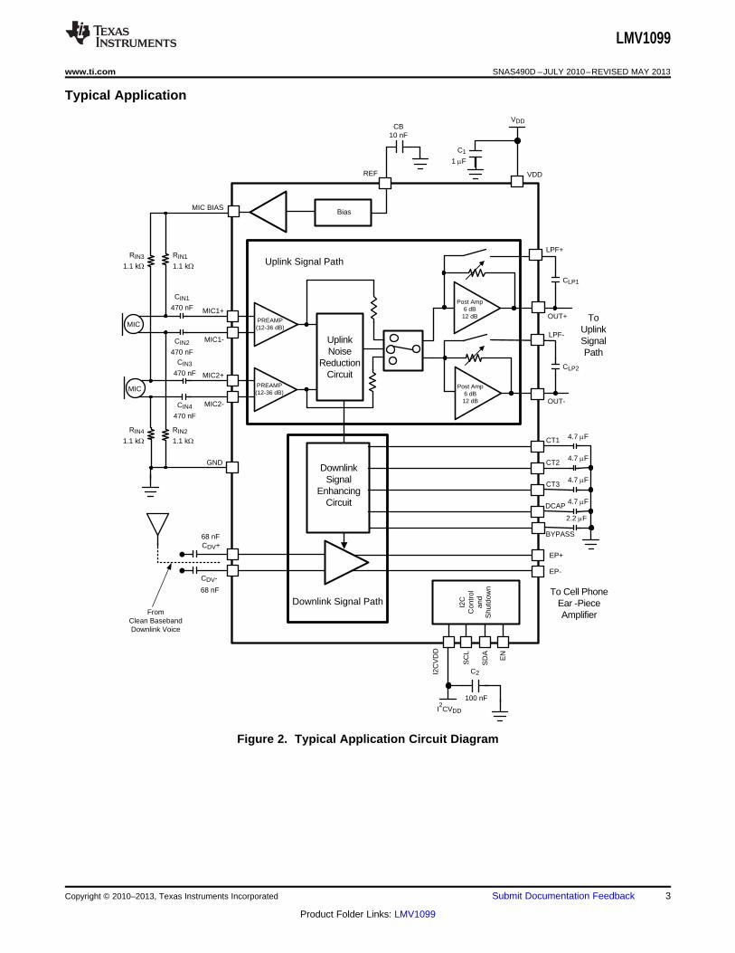
MIC
FromClean BasebandDownlink Voice
AGCAmplifier
AmbientNoise
Uplink Signal Path
Downlink Signal Path
PREAMP
LMV1099 VDD
REFMIC BIASGND
SCL
SDA
EN
CT1
DCAP
BYPASS
DownlinkSignal
EnhancingCircuit
UplinkNoise
ReductionCircuit
ToUplinkSignalPath
ToCell PhoneEar -PieceAmplifier
CT2
CT3
EP+
EP-
DV+
DV-
OUT+
LPF-
LPF+
OUT-
Near-FieldVoice
I2CVDD I2CControl
&Shutdown
PREAMP
MIC 2-
MIC 2+
MIC
MIC 1-
MIC 1+
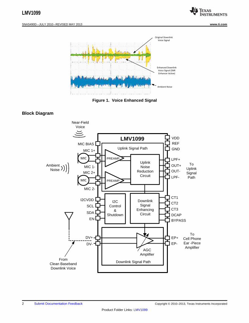
Original Downlink
Voice Signal
Enhanced Downlink
Voice Signal (SNR
Enhancer Active)
Ambient Noise
LMV1099
SNAS490D –JULY 2010–REVISED MAY 2013 www.ti.com
Figure 1. Voice Enhanced Signal
Block Diagram
2 Submit Documentation Feedback Copyright © 2010–2013, Texas Instruments Incorporated
Product Folder Links: LMV1099
MIC
FromClean BasebandDownlink Voice
Uplink Signal Path
Downlink Signal Path
CDV+
MIC2+
MIC
MIC BIAS
LPF+
CT1
BYPASS
REF
GND
EP-
Bias
CIN2
470 nF
VDD
DCAP
DownlinkSignal
EnhancingCircuit
UplinkNoise
ReductionCircuit
ToUplinkSignalPath
To Cell PhoneEar -PieceAmplifier
I2C
Con
trol
and
Shu
tdow
n
CIN1
470 nF
CIN3
470 nF
CIN4
470 nF
RIN1
1.1 k:
RIN3
1.1 k:
RIN2
1.1 k:
RIN4
1.1 k:
C2
EP+
100 nF
SD
A
EN
SC
L
I2C
VD
D
I2CVDD
CB10 nF
VDD
C1
1 PF
CLP1
CLP2
OUT+
LPF-
OUT-
CT2
CT3
MIC2-
MIC1+
MIC1-
PREAMP(12-36 dB)
PREAMP(12-36 dB)
Post Amp6 dB12 dB
Post Amp6 dB
12 dB
4.7 PF
4.7 PF
4.7 PF
4.7 PF
2.2 PF
CDV-
68 nF
68 nF
LMV1099
www.ti.com SNAS490D –JULY 2010–REVISED MAY 2013
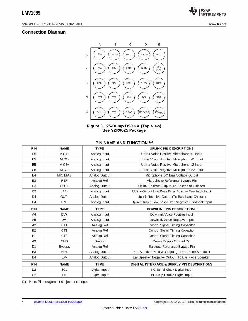
Typical Application
Figure 2. Typical Application Circuit Diagram
Copyright © 2010–2013, Texas Instruments Incorporated Submit Documentation Feedback 3
Product Folder Links: LMV1099
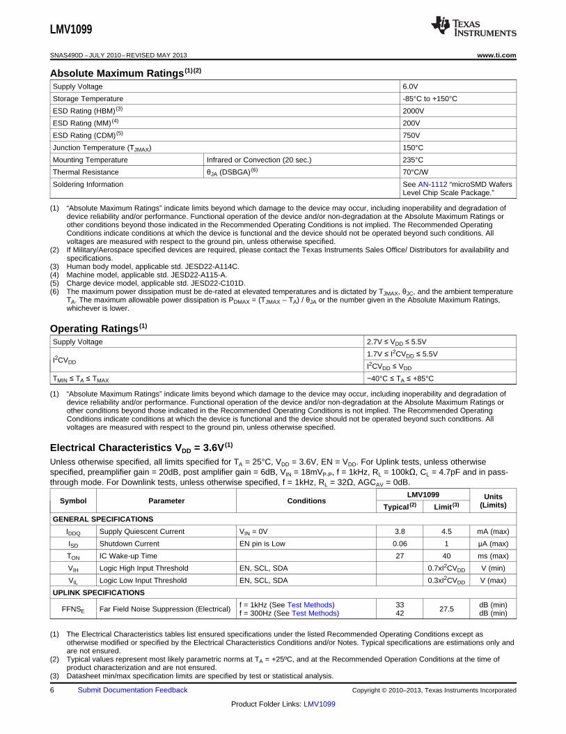
A DCB
5
2
3
4
1
E
VDD
CT1
GND
DV+
DV-
CT3 DCAP BYPASS
CT2 EN SCL SDA
OUT+LPF+EP+ REF
MICBIAS
MIC1-MIC1+MIC2-MIC2+
EP- LPF- OUT-
I2CVDD
LMV1099
SNAS490D –JULY 2010–REVISED MAY 2013 www.ti.com
Connection Diagram
Figure 3. 25-Bump DSBGA (Top View)See YZR0025 Package
PIN NAME AND FUNCTION (1)
PIN NAME TYPE UPLINK PIN DESCRIPTIONS
D5 MIC1+ Analog Input Uplink Voice Positive Microphone #1 Input
E5 MIC1- Analog Input Uplink Voice Negative Microphone #1 Input
B5 MIC2+ Analog Input Uplink Voice Positive Microphone #2 Input
C5 MIC2- Analog Input Uplink Voice Negative Microphone #2 Input
E4 MIC BIAS Analog Output Microphone DC Bias Voltage Output
E3 REF Analog Ref Microphone Reference Bypass Pin
D3 OUT+ Analog Output Uplink Positive Output (To Baseband Chipset)
C3 LPF+ Analog Input Uplink-Output Low Pass Filter Positive Feedback Input
D4 OUT- Analog Output Uplink Negative Output (To Baseband Chipset)
C4 LPF- Analog Input Uplink-Output Low Pass Filter Negative Feedback Input
PIN NAME TYPE DOWNLINK PIN DESCRIPTIONS
A4 DV+ Analog Input Downlink Voice Positive Input
A5 DV- Analog Input Downlink Voice Negative Input
A2 CT1 Analog Ref Control Signal Timing Capacitor
B2 CT2 Analog Ref Control Signal Timing Capacitor
B1 CT3 Analog Ref Control Signal Timing Capacitor
A3 GND Ground Power Supply Ground Pin
D1 Bypass Analog Ref Earpiece Reference Bypass Pin
B3 EP+ Analog Output Ear Speaker Positive Output (To Ear Piece Speaker)
B4 EP- Analog Output Ear Speaker Negative Output (To Ear Piece Speaker)
PIN NAME TYPE DIGITAL INTERFACE & SUPPLY PIN DESCRIPTIONS
D2 SCL Digital Input I2C Serial Clock Digital Input
C2 EN Digital Input I2C Chip Enable Digital Input
(1) Note: Pin assignment subject to change.
4 Submit Documentation Feedback Copyright © 2010–2013, Texas Instruments Incorporated
Product Folder Links: LMV1099

LMV1099
www.ti.com SNAS490D –JULY 2010–REVISED MAY 2013
PIN NAME AND FUNCTION (1) (continued)
PIN NAME TYPE UPLINK PIN DESCRIPTIONS
E2 SDA Digital I/O I2C Serial Data Address Digital Input/Output Pin
E1 I2CVDD Digital Supply I2C Digital Supply Voltage Pin
A1 VDD Supply Power Supply Voltage Pin
C1 DCAP Analog Ref Voice Signal Detection Capacitor
These devices have limited built-in ESD protection. The leads should be shorted together or the device placed in conductive foamduring storage or handling to prevent electrostatic damage to the MOS gates.
Copyright © 2010–2013, Texas Instruments Incorporated Submit Documentation Feedback 5
Product Folder Links: LMV1099
LMV1099
SNAS490D –JULY 2010–REVISED MAY 2013 www.ti.com
Absolute Maximum Ratings (1) (2)
Supply Voltage 6.0V
Storage Temperature -85°C to +150°C
ESD Rating (HBM) (3) 2000V
ESD Rating (MM) (4) 200V
ESD Rating (CDM) (5) 750V
Junction Temperature (TJMAX) 150°C
Mounting Temperature Infrared or Convection (20 sec.) 235°C
Thermal Resistance θJA (DSBGA) (6) 70°C/W
Soldering Information See AN-1112 “microSMD WafersLevel Chip Scale Package.”
(1) “Absolute Maximum Ratings” indicate limits beyond which damage to the device may occur, including inoperability and degradation ofdevice reliability and/or performance. Functional operation of the device and/or non-degradation at the Absolute Maximum Ratings orother conditions beyond those indicated in the Recommended Operating Conditions is not implied. The Recommended OperatingConditions indicate conditions at which the device is functional and the device should not be operated beyond such conditions. Allvoltages are measured with respect to the ground pin, unless otherwise specified.
(2) If Military/Aerospace specified devices are required, please contact the Texas Instruments Sales Office/ Distributors for availability andspecifications.
(3) Human body model, applicable std. JESD22-A114C.(4) Machine model, applicable std. JESD22-A115-A.(5) Charge device model, applicable std. JESD22-C101D.(6) The maximum power dissipation must be de-rated at elevated temperatures and is dictated by TJMAX, θJC, and the ambient temperature
TA. The maximum allowable power dissipation is PDMAX = (TJMAX – TA) / θJA or the number given in the Absolute Maximum Ratings,whichever is lower.
Operating Ratings (1)
Supply Voltage 2.7V ≤ VDD ≤ 5.5V
1.7V ≤ I2CVDD ≤ 5.5VI2CVDD
I2CVDD ≤ VDD
TMIN ≤ TA ≤ TMAX −40°C ≤ TA ≤ +85°C
(1) “Absolute Maximum Ratings” indicate limits beyond which damage to the device may occur, including inoperability and degradation ofdevice reliability and/or performance. Functional operation of the device and/or non-degradation at the Absolute Maximum Ratings orother conditions beyond those indicated in the Recommended Operating Conditions is not implied. The Recommended OperatingConditions indicate conditions at which the device is functional and the device should not be operated beyond such conditions. Allvoltages are measured with respect to the ground pin, unless otherwise specified.
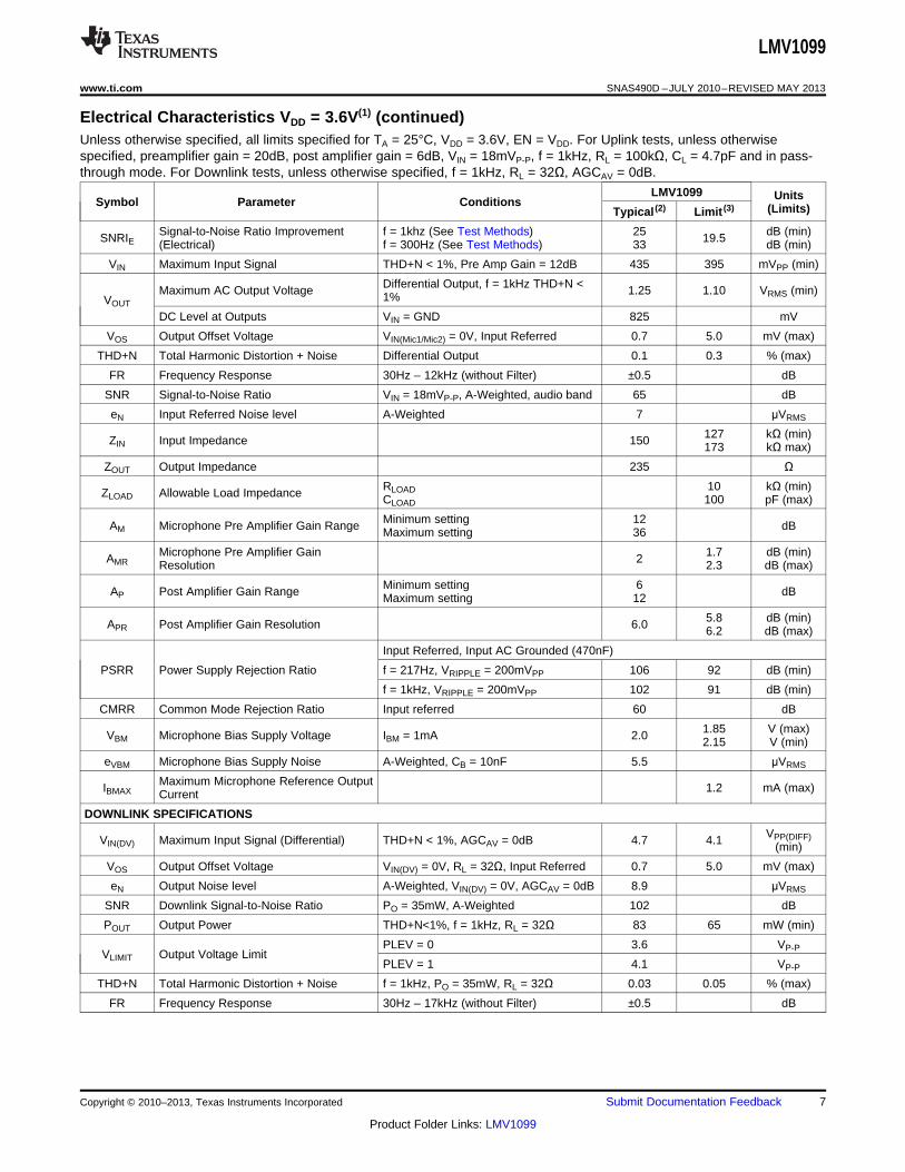
Electrical Characteristics VDD = 3.6V (1)
Unless otherwise specified, all limits specified for TA = 25°C, VDD = 3.6V, EN = VDD. For Uplink tests, unless otherwisespecified, preamplifier gain = 20dB, post amplifier gain = 6dB, VIN = 18mVP-P, f = 1kHz, RL = 100kΩ, CL = 4.7pF and in pass-through mode. For Downlink tests, unless otherwise specified, f = 1kHz, RL = 32Ω, AGCAV = 0dB.
LMV1099 UnitsSymbol Parameter Conditions (Limits)Typical (2) Limit (3)
GENERAL SPECIFICATIONS
IDDQ Supply Quiescent Current VIN = 0V 3.8 4.5 mA (max)
ISD Shutdown Current EN pin is Low 0.06 1 μA (max)
TON IC Wake-up Time 27 40 ms (max)
VIH Logic High Input Threshold EN, SCL, SDA 0.7xI2CVDD V (min)
VIL Logic Low Input Threshold EN, SCL, SDA 0.3xI2CVDD V (max)
UPLINK SPECIFICATIONS
f = 1kHz (See Test Methods) 33 dB (min)FFNSE Far Field Noise Suppression (Electrical) 27.5f = 300Hz (See Test Methods) 42 dB (min)
(1) The Electrical Characteristics tables list ensured specifications under the listed Recommended Operating Conditions except asotherwise modified or specified by the Electrical Characteristics Conditions and/or Notes. Typical specifications are estimations only andare not ensured.
(2) Typical values represent most likely parametric norms at TA = +25ºC, and at the Recommended Operation Conditions at the time ofproduct characterization and are not ensured.
(3) Datasheet min/max specification limits are specified by test or statistical analysis.
6 Submit Documentation Feedback Copyright © 2010–2013, Texas Instruments Incorporated
Product Folder Links: LMV1099
LMV1099
www.ti.com SNAS490D –JULY 2010–REVISED MAY 2013
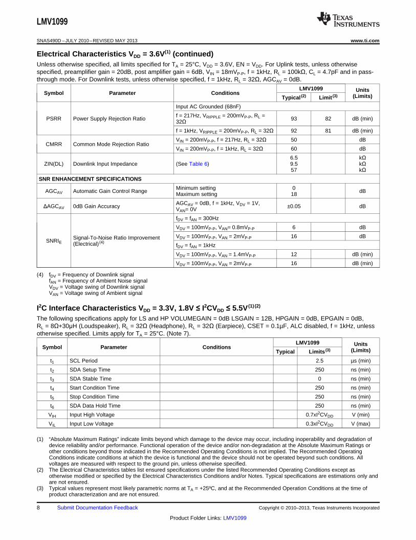
Electrical Characteristics VDD = 3.6V(1) (continued)Unless otherwise specified, all limits specified for TA = 25°C, VDD = 3.6V, EN = VDD. For Uplink tests, unless otherwisespecified, preamplifier gain = 20dB, post amplifier gain = 6dB, VIN = 18mVP-P, f = 1kHz, RL = 100kΩ, CL = 4.7pF and in pass-through mode. For Downlink tests, unless otherwise specified, f = 1kHz, RL = 32Ω, AGCAV = 0dB.
LMV1099 UnitsSymbol Parameter Conditions (Limits)Typical (2) Limit (3)
Signal-to-Noise Ratio Improvement f = 1khz (See Test Methods) 25 dB (min)SNRIE 19.5(Electrical) f = 300Hz (See Test Methods) 33 dB (min)
VIN Maximum Input Signal THD+N < 1%, Pre Amp Gain = 12dB 435 395 mVPP (min)
Differential Output, f = 1kHz THD+N <Maximum AC Output Voltage 1.25 1.10 VRMS (min)1%VOUT
DC Level at Outputs VIN = GND 825 mV
VOS Output Offset Voltage VIN(Mic1/Mic2) = 0V, Input Referred 0.7 5.0 mV (max)
THD+N Total Harmonic Distortion + Noise Differential Output 0.1 0.3 % (max)
FR Frequency Response 30Hz – 12kHz (without Filter) ±0.5 dB
SNR Signal-to-Noise Ratio VIN = 18mVP-P, A-Weighted, audio band 65 dB
eN Input Referred Noise level A-Weighted 7 μVRMS
127 kΩ (min)ZIN Input Impedance 150 173 kΩ max)
ZOUT Output Impedance 235 ΩRLOAD 10 kΩ (min)ZLOAD Allowable Load Impedance CLOAD 100 pF (max)
Minimum setting 12AM Microphone Pre Amplifier Gain Range dBMaximum setting 36
Microphone Pre Amplifier Gain 1.7 dB (min)AMR 2Resolution 2.3 dB (max)
Minimum setting 6AP Post Amplifier Gain Range dBMaximum setting 12
5.8 dB (min)APR Post Amplifier Gain Resolution 6.0 6.2 dB (max)
Input Referred, Input AC Grounded (470nF)
PSRR Power Supply Rejection Ratio f = 217Hz, VRIPPLE = 200mVPP 106 92 dB (min)
f = 1kHz, VRIPPLE = 200mVPP 102 91 dB (min)
CMRR Common Mode Rejection Ratio Input referred 60 dB
1.85 V (max)VBM Microphone Bias Supply Voltage IBM = 1mA 2.0 2.15 V (min)
eVBM Microphone Bias Supply Noise A-Weighted, CB = 10nF 5.5 μVRMS
Maximum Microphone Reference OutputIBMAX 1.2 mA (max)Current
DOWNLINK SPECIFICATIONS
VPP(DIFF)VIN(DV) Maximum Input Signal (Differential) THD+N < 1%, AGCAV = 0dB 4.7 4.1 (min)
VOS Output Offset Voltage VIN(DV) = 0V, RL = 32Ω, Input Referred 0.7 5.0 mV (max)
eN Output Noise level A-Weighted, VIN(DV) = 0V, AGCAV = 0dB 8.9 μVRMS
SNR Downlink Signal-to-Noise Ratio PO = 35mW, A-Weighted 102 dB
POUT Output Power THD+N<1%, f = 1kHz, RL = 32Ω 83 65 mW (min)
PLEV = 0 3.6 VP-PVLIMIT Output Voltage Limit
PLEV = 1 4.1 VP-P
THD+N Total Harmonic Distortion + Noise f = 1kHz, PO = 35mW, RL = 32Ω 0.03 0.05 % (max)
FR Frequency Response 30Hz – 17kHz (without Filter) ±0.5 dB
Copyright © 2010–2013, Texas Instruments Incorporated Submit Documentation Feedback 7
Product Folder Links: LMV1099
LMV1099
SNAS490D –JULY 2010–REVISED MAY 2013 www.ti.com
Electrical Characteristics VDD = 3.6V(1) (continued)Unless otherwise specified, all limits specified for TA = 25°C, VDD = 3.6V, EN = VDD. For Uplink tests, unless otherwisespecified, preamplifier gain = 20dB, post amplifier gain = 6dB, VIN = 18mVP-P, f = 1kHz, RL = 100kΩ, CL = 4.7pF and in pass-through mode. For Downlink tests, unless otherwise specified, f = 1kHz, RL = 32Ω, AGCAV = 0dB.
LMV1099 UnitsSymbol Parameter Conditions (Limits)Typical (2) Limit (3)
Input AC Grounded (68nF)
f = 217Hz, VRIPPLE = 200mVP-P, RL =PSRR Power Supply Rejection Ratio 93 82 dB (min)32Ωf = 1kHz, VRIPPLE = 200mVP-P, RL = 32Ω 92 81 dB (min)
VIN = 200mVP-P, f = 217Hz, RL = 32Ω 50 dBCMRR Common Mode Rejection Ratio
VIN = 200mVP-P, f = 1kHz, RL = 32Ω 60 dB
6.5 kΩZIN(DL) Downlink Input Impedance (See Table 6) 9.5 kΩ
57 kΩSNR ENHANCEMENT SPECIFICATIONS
Minimum setting 0AGCAV Automatic Gain Control Range dBMaximum setting 18
AGCAV = 0dB, f = 1kHz, VDV = 1V,ΔAGCAV 0dB Gain Accuracy ±0.05 dBVAN= 0V
fDV = fAN = 300Hz
VDV = 100mVP-P, VAN= 0.8mVP-P 6 dB
VDV = 100mVP-P, VAN = 2mVP-P 16 dBSignal-To-Noise Ratio ImprovementSNRIE (Electrical) (4)fDV = fAN = 1kHz
VDV = 100mVP-P, VAN = 1.4mVP-P 12 dB (min)
VDV = 100mVP-P, VAN = 2mVP-P 16 dB (min)
(4) fDV = Frequency of Downlink signalfAN = Frequency of Ambient Noise signalVDV = Voltage swing of Downlink signalVAN = Voltage swing of Ambient signal
I2C Interface Characteristics VDD = 3.3V, 1.8V ≤ I2CVDD ≤ 5.5V (1) (2)
The following specifications apply for LS and HP VOLUMEGAIN = 0dB LSGAIN = 12B, HPGAIN = 0dB, EPGAIN = 0dB,RL = 8Ω+30μH (Loudspeaker), RL = 32Ω (Headphone), RL = 32Ω (Earpiece), CSET = 0.1µF, ALC disabled, f = 1kHz, unlessotherwise specified. Limits apply for TA = 25°C. (Note 7).
LMV1099 UnitsSymbol Parameter Conditions (Limits)Typical Limits (3)
t1 SCL Period 2.5 µs (min)
t2 SDA Setup Time 250 ns (min)
t3 SDA Stable Time 0 ns (min)
t4 Start Condition Time 250 ns (min)
t5 Stop Condition Time 250 ns (min)
t6 SDA Data Hold Time 250 ns (min)
VIH Input High Voltage 0.7xI2CVDD V (min)
VIL Input Low Voltage 0.3xI2CVDD V (max)
(1) “Absolute Maximum Ratings” indicate limits beyond which damage to the device may occur, including inoperability and degradation ofdevice reliability and/or performance. Functional operation of the device and/or non-degradation at the Absolute Maximum Ratings orother conditions beyond those indicated in the Recommended Operating Conditions is not implied. The Recommended OperatingConditions indicate conditions at which the device is functional and the device should not be operated beyond such conditions. Allvoltages are measured with respect to the ground pin, unless otherwise specified.
(2) The Electrical Characteristics tables list ensured specifications under the listed Recommended Operating Conditions except asotherwise modified or specified by the Electrical Characteristics Conditions and/or Notes. Typical specifications are estimations only andare not ensured.
(3) Typical values represent most likely parametric norms at TA = +25ºC, and at the Recommended Operation Conditions at the time ofproduct characterization and are not ensured.
8 Submit Documentation Feedback Copyright © 2010–2013, Texas Instruments Incorporated
Product Folder Links: LMV1099
Mic2+
Mic2-
Mic1+
Mic1-
470 nF
470 nF
470 nF
470 nFOUT-
LPF
LMV1099
OUT+Osc2
Osc1
AC Voltmeter
LMV1099
www.ti.com SNAS490D –JULY 2010–REVISED MAY 2013
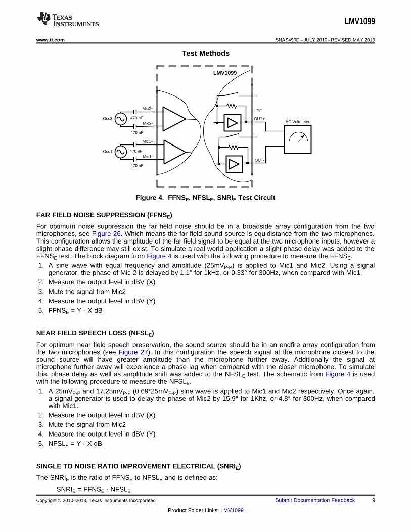
Test Methods
Figure 4. FFNSE, NFSLE, SNRIE Test Circuit
FAR FIELD NOISE SUPPRESSION (FFNSE)
For optimum noise suppression the far field noise should be in a broadside array configuration from the twomicrophones, see Figure 26. Which means the far field sound source is equidistance from the two microphones.This configuration allows the amplitude of the far field signal to be equal at the two microphone inputs, however aslight phase difference may still exist. To simulate a real world application a slight phase delay was added to theFFNSE test. The block diagram from Figure 4 is used with the following procedure to measure the FFNSE.1. A sine wave with equal frequency and amplitude (25mVP-P) is applied to Mic1 and Mic2. Using a signal
generator, the phase of Mic 2 is delayed by 1.1° for 1kHz, or 0.33° for 300Hz, when compared with Mic1.2. Measure the output level in dBV (X)3. Mute the signal from Mic24. Measure the output level in dBV (Y)5. FFNSE = Y - X dB
NEAR FIELD SPEECH LOSS (NFSLE)
For optimum near field speech preservation, the sound source should be in an endfire array configuration fromthe two microphones (see Figure 27). In this configuration the speech signal at the microphone closest to thesound source will have greater amplitude than the microphone further away. Additionally the signal atmicrophone further away will experience a phase lag when compared with the closer microphone. To simulatethis, phase delay as well as amplitude shift was added to the NFSLE test. The schematic from Figure 4 is usedwith the following procedure to measure the NFSLE.1. A 25mVP-P and 17.25mVP-P (0.69*25mVP-P) sine wave is applied to Mic1 and Mic2 respectively. Once again,
a signal generator is used to delay the phase of Mic2 by 15.9° for 1Khz, or 4.8° for 300Hz, when comparedwith Mic1.
2. Measure the output level in dBV (X)3. Mute the signal from Mic24. Measure the output level in dBV (Y)5. NFSLE = Y - X dB
SINGLE TO NOISE RATIO IMPROVEMENT ELECTRICAL (SNRIE)
The SNRIE is the ratio of FFNSE to NFSLE and is defined as:
SNRIE = FFNSE - NFSLE
Copyright © 2010–2013, Texas Instruments Incorporated Submit Documentation Feedback 9
Product Folder Links: LMV1099
0.001
0.01
0.1
1
10
100
10 100 1000 10000 100000
FREQUENCY (Hz)
TH
D+
N (
%)
0.001
0.01
0.1
1
10
100
10 100 1000 10000 100000
FREQUENCY (Hz)
TH
D+
N (
%)
0.001
0.01
0.1
1
10
100
10 100 1000 10000 100000
FREQUENCY (Hz)
TH
D+
N (
%)
0.001
0.01
0.1
1
10
100
10 100 1000 10000 100000
FREQUENCY (Hz)
TH
D+
N (
%)
0.001
0.01
0.1
1
10
100
10 100 1000 10000 100000
FREQUENCY (Hz)
TH
D+
N (
%)
0.001
0.01
0.1
1
10
100
10 100 1000 10000 100000
FREQUENCY (Hz)
TH
D+
N (
%)
LMV1099
SNAS490D –JULY 2010–REVISED MAY 2013 www.ti.com
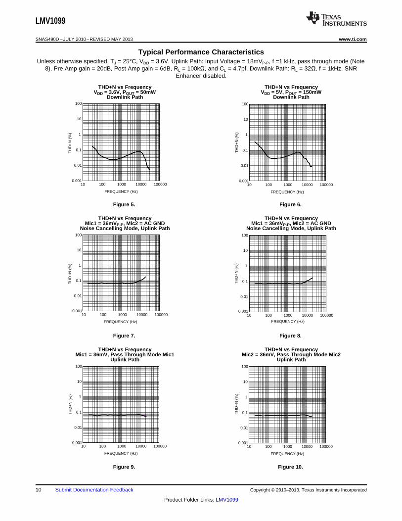
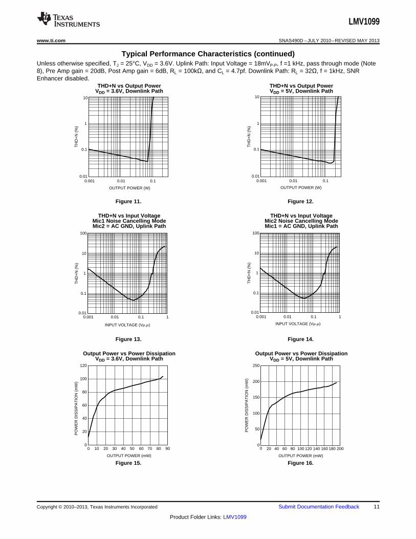
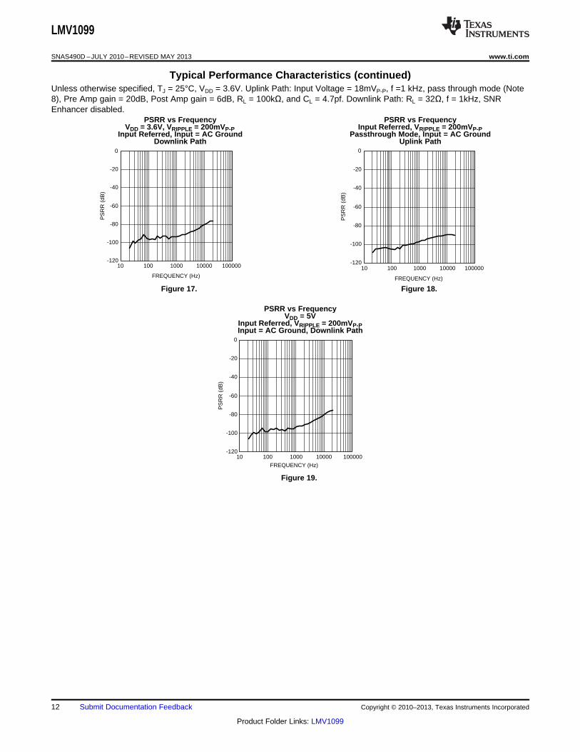
Typical Performance CharacteristicsUnless otherwise specified, TJ = 25°C, VDD = 3.6V. Uplink Path: Input Voltage = 18mVP-P, f =1 kHz, pass through mode (Note
8), Pre Amp gain = 20dB, Post Amp gain = 6dB, RL = 100kΩ, and CL = 4.7pf. Downlink Path: RL = 32Ω, f = 1kHz, SNREnhancer disabled.
THD+N vs Frequency THD+N vs FrequencyVDD = 3.6V, POUT = 50mW VDD = 5V, POUT = 150mW
Downlink Path Downlink Path
Figure 5. Figure 6.
THD+N vs Frequency THD+N vs FrequencyMic1 = 36mVP-P, Mic2 = AC GND Mic1 = 36mVP-P, Mic2 = AC GND
Noise Cancelling Mode, Uplink Path Noise Cancelling Mode, Uplink Path
Figure 7. Figure 8.
THD+N vs Frequency THD+N vs FrequencyMic1 = 36mV, Pass Through Mode Mic1 Mic2 = 36mV, Pass Through Mode Mic2
Uplink Path Uplink Path
Figure 9. Figure 10.
10 Submit Documentation Feedback Copyright © 2010–2013, Texas Instruments Incorporated
Product Folder Links: LMV1099
0
20
40
60
80
100
120
0 10 20 30 40 50 60 70 80 90
OUTPUT POWER (mW)
PO
WE
R D
ISS
IPA
TIO
N (
mW
)
0
50
100
150
200
250
0 20 40 60 80 100 120 140 160 180 200
OUTPUT POWER (mW)
PO
WE
R D
ISS
IPA
TIO
N (
mW
)
0.01
0.1
1
10
100
0.001 0.01 0.1 1
TH
D+
N (
%)
INPUT VOLTAGE (VP-P)
0.01
0.1
1
10
100
0.001 0.01 0.1 1
TH
D+
N (
%)
INPUT VOLTAGE (VP-P)
0.01
0.1
1
10
0.001 0.01 0.1
OUTPUT POWER (W)
TH
D+
N (
%)
0.01
0.1
1
10
0.001 0.01 0.1
OUTPUT POWER (W)
TH
D+
N (
%)
LMV1099
www.ti.com SNAS490D –JULY 2010–REVISED MAY 2013
Typical Performance Characteristics (continued)Unless otherwise specified, TJ = 25°C, VDD = 3.6V. Uplink Path: Input Voltage = 18mVP-P, f =1 kHz, pass through mode (Note8), Pre Amp gain = 20dB, Post Amp gain = 6dB, RL = 100kΩ, and CL = 4.7pf. Downlink Path: RL = 32Ω, f = 1kHz, SNREnhancer disabled.
THD+N vs Output Power THD+N vs Output PowerVDD = 3.6V, Downlink Path VDD = 5V, Downlink Path
Figure 11. Figure 12.
THD+N vs Input Voltage THD+N vs Input VoltageMic1 Noise Cancelling Mode Mic2 Noise Cancelling ModeMic2 = AC GND, Uplink Path Mic1 = AC GND, Uplink Path
Figure 13. Figure 14.
Output Power vs Power Dissipation Output Power vs Power DissipationVDD = 3.6V, Downlink Path VDD = 5V, Downlink Path
Figure 15. Figure 16.
Copyright © 2010–2013, Texas Instruments Incorporated Submit Documentation Feedback 11
Product Folder Links: LMV1099
-120
-100
-80
-60
-40
-20
0
10 100 1000 10000 100000
FREQUENCY (Hz)
PS
RR
(dB
)
-120
-100
-80
-60
-40
-20
0
10 100 1000 10000 100000
FREQUENCY (Hz)
PS
RR
(dB
)
-120
-100
-80
-60
-40
-20
0
10 100 1000 10000 100000
FREQUENCY (Hz)
PS
RR
(dB
)
LMV1099
SNAS490D –JULY 2010–REVISED MAY 2013 www.ti.com
Typical Performance Characteristics (continued)Unless otherwise specified, TJ = 25°C, VDD = 3.6V. Uplink Path: Input Voltage = 18mVP-P, f =1 kHz, pass through mode (Note8), Pre Amp gain = 20dB, Post Amp gain = 6dB, RL = 100kΩ, and CL = 4.7pf. Downlink Path: RL = 32Ω, f = 1kHz, SNREnhancer disabled.
PSRR vs Frequency PSRR vs FrequencyVDD = 3.6V, VRIPPLE = 200mVP-P Input Referred, VRIPPLE = 200mVP-P
Input Referred, Input = AC Ground Passthrough Mode, Input = AC GroundDownlink Path Uplink Path
Figure 17. Figure 18.
PSRR vs FrequencyVDD = 5V
Input Referred, VRIPPLE = 200mVP-PInput = AC Ground, Downlink Path
Figure 19.
12 Submit Documentation Feedback Copyright © 2010–2013, Texas Instruments Incorporated
Product Folder Links: LMV1099
Analog Noise
CancellingBlock
Optimized Audio Ouput
OUT+
Post Amp Gain(6 dB / 12 dB)
Pre Amp Gain(12 dB - 36 dB)
Mic1or
Mic2
Gain(Max. 0 dB)
OUT-
MaximumAC Input Voltage
<1.6 Vpp
MaximumAC Output
Voltage<3.2 Vpp
Maximum AC Input Voltage
<440 mVpp
MaximumAC Intput Voltage
<1.6 Vpp
Analog Noise
CancellingBlock
Optimized Audio Ouput
OUT+
Post Amp Gain(6 dB / 12 dB)
Preamp Gain(12 dB - 36 dB)
Mic1
OUT-
Mic2
LMV1099
www.ti.com SNAS490D –JULY 2010–REVISED MAY 2013
APPLICATION DATA
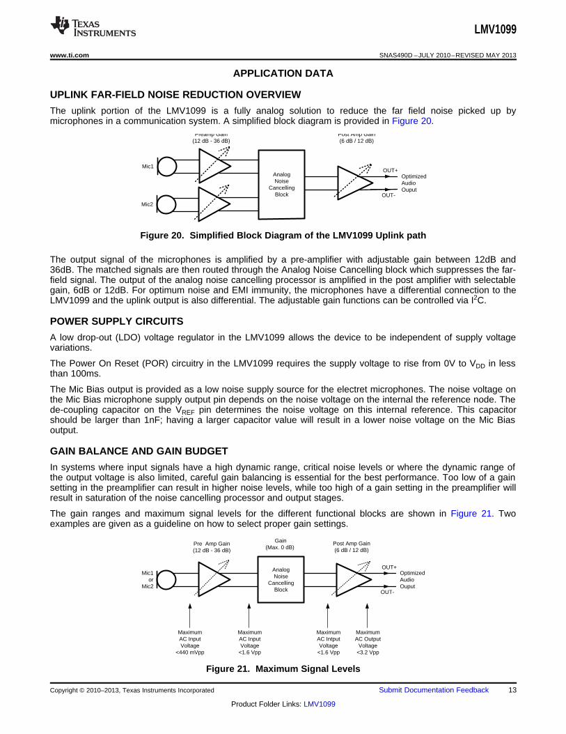
UPLINK FAR-FIELD NOISE REDUCTION OVERVIEW
The uplink portion of the LMV1099 is a fully analog solution to reduce the far field noise picked up bymicrophones in a communication system. A simplified block diagram is provided in Figure 20.
Figure 20. Simplified Block Diagram of the LMV1099 Uplink path
The output signal of the microphones is amplified by a pre-amplifier with adjustable gain between 12dB and36dB. The matched signals are then routed through the Analog Noise Cancelling block which suppresses the far-field signal. The output of the analog noise cancelling processor is amplified in the post amplifier with selectablegain, 6dB or 12dB. For optimum noise and EMI immunity, the microphones have a differential connection to theLMV1099 and the uplink output is also differential. The adjustable gain functions can be controlled via I2C.
POWER SUPPLY CIRCUITS
A low drop-out (LDO) voltage regulator in the LMV1099 allows the device to be independent of supply voltagevariations.
The Power On Reset (POR) circuitry in the LMV1099 requires the supply voltage to rise from 0V to VDD in lessthan 100ms.
The Mic Bias output is provided as a low noise supply source for the electret microphones. The noise voltage onthe Mic Bias microphone supply output pin depends on the noise voltage on the internal the reference node. Thede-coupling capacitor on the VREF pin determines the noise voltage on this internal reference. This capacitorshould be larger than 1nF; having a larger capacitor value will result in a lower noise voltage on the Mic Biasoutput.
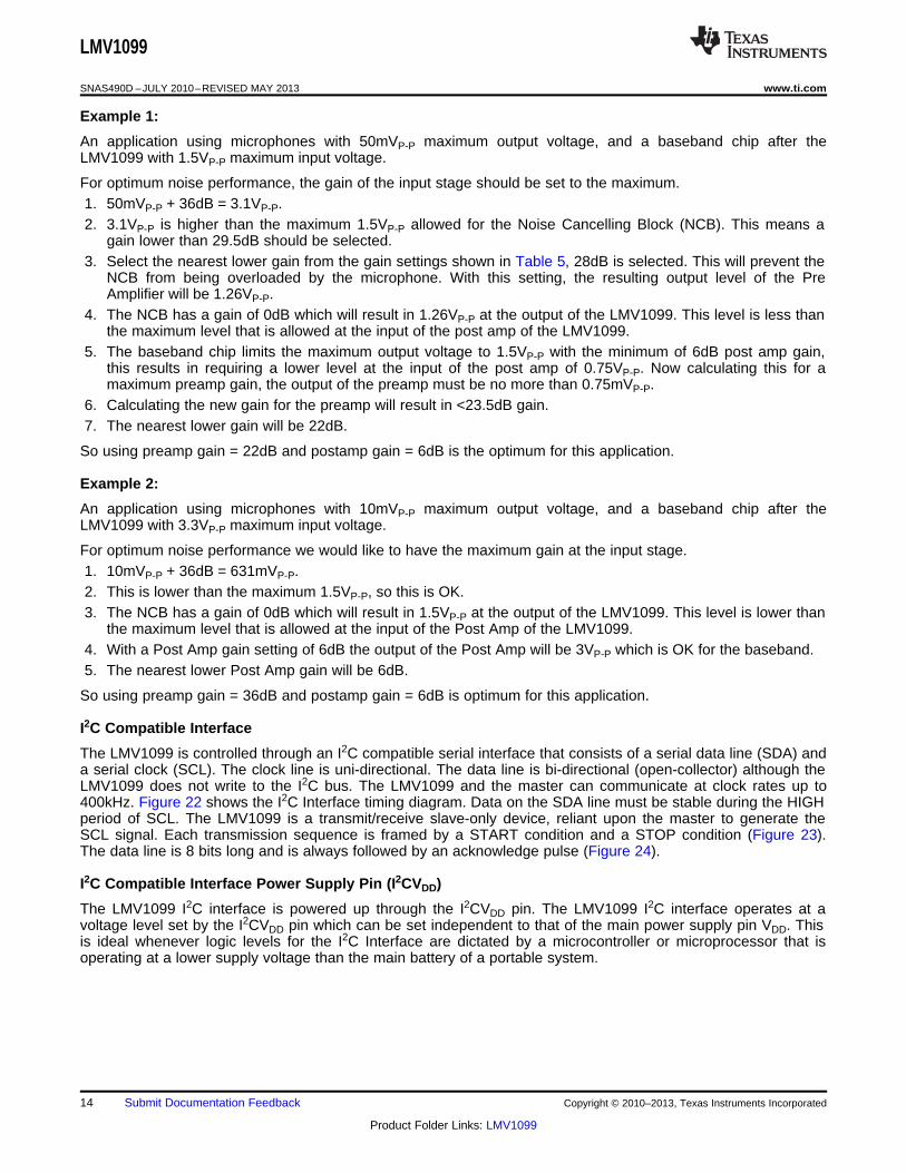
GAIN BALANCE AND GAIN BUDGET
In systems where input signals have a high dynamic range, critical noise levels or where the dynamic range ofthe output voltage is also limited, careful gain balancing is essential for the best performance. Too low of a gainsetting in the preamplifier can result in higher noise levels, while too high of a gain setting in the preamplifier willresult in saturation of the noise cancelling processor and output stages.
The gain ranges and maximum signal levels for the different functional blocks are shown in Figure 21. Twoexamples are given as a guideline on how to select proper gain settings.
Figure 21. Maximum Signal Levels
Copyright © 2010–2013, Texas Instruments Incorporated Submit Documentation Feedback 13
Product Folder Links: LMV1099
LMV1099
SNAS490D –JULY 2010–REVISED MAY 2013 www.ti.com
Example 1:
An application using microphones with 50mVP-P maximum output voltage, and a baseband chip after theLMV1099 with 1.5VP-P maximum input voltage.
For optimum noise performance, the gain of the input stage should be set to the maximum.1. 50mVP-P + 36dB = 3.1VP-P.2. 3.1VP-P is higher than the maximum 1.5VP-P allowed for the Noise Cancelling Block (NCB). This means a
gain lower than 29.5dB should be selected.3. Select the nearest lower gain from the gain settings shown in Table 5, 28dB is selected. This will prevent the
NCB from being overloaded by the microphone. With this setting, the resulting output level of the PreAmplifier will be 1.26VP-P.
4. The NCB has a gain of 0dB which will result in 1.26VP-P at the output of the LMV1099. This level is less thanthe maximum level that is allowed at the input of the post amp of the LMV1099.
5. The baseband chip limits the maximum output voltage to 1.5VP-P with the minimum of 6dB post amp gain,this results in requiring a lower level at the input of the post amp of 0.75VP-P. Now calculating this for amaximum preamp gain, the output of the preamp must be no more than 0.75mVP-P.
6. Calculating the new gain for the preamp will result in <23.5dB gain.7. The nearest lower gain will be 22dB.
So using preamp gain = 22dB and postamp gain = 6dB is the optimum for this application.
Example 2:
An application using microphones with 10mVP-P maximum output voltage, and a baseband chip after theLMV1099 with 3.3VP-P maximum input voltage.
For optimum noise performance we would like to have the maximum gain at the input stage.1. 10mVP-P + 36dB = 631mVP-P.2. This is lower than the maximum 1.5VP-P, so this is OK.3. The NCB has a gain of 0dB which will result in 1.5VP-P at the output of the LMV1099. This level is lower than
the maximum level that is allowed at the input of the Post Amp of the LMV1099.4. With a Post Amp gain setting of 6dB the output of the Post Amp will be 3VP-P which is OK for the baseband.5. The nearest lower Post Amp gain will be 6dB.
So using preamp gain = 36dB and postamp gain = 6dB is optimum for this application.
I2C Compatible Interface
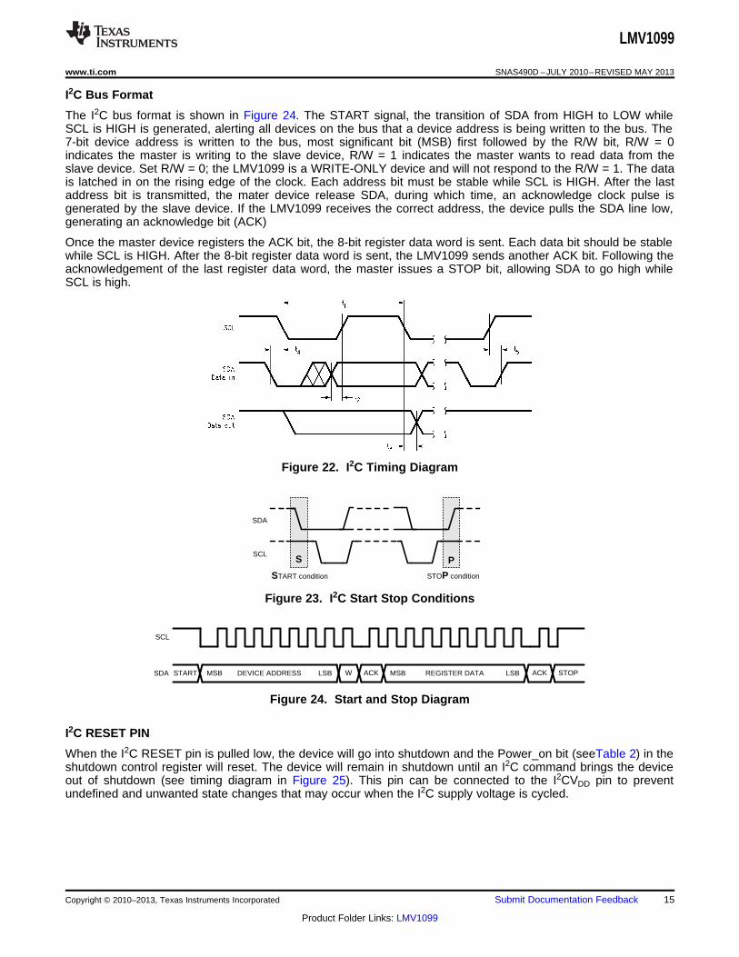
The LMV1099 is controlled through an I2C compatible serial interface that consists of a serial data line (SDA) anda serial clock (SCL). The clock line is uni-directional. The data line is bi-directional (open-collector) although theLMV1099 does not write to the I2C bus. The LMV1099 and the master can communicate at clock rates up to400kHz. Figure 22 shows the I2C Interface timing diagram. Data on the SDA line must be stable during the HIGHperiod of SCL. The LMV1099 is a transmit/receive slave-only device, reliant upon the master to generate theSCL signal. Each transmission sequence is framed by a START condition and a STOP condition (Figure 23).The data line is 8 bits long and is always followed by an acknowledge pulse (Figure 24).
I2C Compatible Interface Power Supply Pin (I2CVDD)
The LMV1099 I2C interface is powered up through the I2CVDD pin. The LMV1099 I2C interface operates at avoltage level set by the I2CVDD pin which can be set independent to that of the main power supply pin VDD. Thisis ideal whenever logic levels for the I2C Interface are dictated by a microcontroller or microprocessor that isoperating at a lower supply voltage than the main battery of a portable system.
14 Submit Documentation Feedback Copyright © 2010–2013, Texas Instruments Incorporated
Product Folder Links: LMV1099
START MSB DEVICE ADDRESS LSB ACK
SCL
SDA STOPMSB REGISTER DATA LSB ACKW
SDA
SCLS P
START condition STOP condition
LMV1099
www.ti.com SNAS490D –JULY 2010–REVISED MAY 2013
I2C Bus Format
The I2C bus format is shown in Figure 24. The START signal, the transition of SDA from HIGH to LOW whileSCL is HIGH is generated, alerting all devices on the bus that a device address is being written to the bus. The7-bit device address is written to the bus, most significant bit (MSB) first followed by the R/W bit, R/W = 0indicates the master is writing to the slave device, R/W = 1 indicates the master wants to read data from theslave device. Set R/W = 0; the LMV1099 is a WRITE-ONLY device and will not respond to the R/W = 1. The datais latched in on the rising edge of the clock. Each address bit must be stable while SCL is HIGH. After the lastaddress bit is transmitted, the mater device release SDA, during which time, an acknowledge clock pulse isgenerated by the slave device. If the LMV1099 receives the correct address, the device pulls the SDA line low,generating an acknowledge bit (ACK)
Once the master device registers the ACK bit, the 8-bit register data word is sent. Each data bit should be stablewhile SCL is HIGH. After the 8-bit register data word is sent, the LMV1099 sends another ACK bit. Following theacknowledgement of the last register data word, the master issues a STOP bit, allowing SDA to go high whileSCL is high.
Figure 22. I2C Timing Diagram
Figure 23. I2C Start Stop Conditions
Figure 24. Start and Stop Diagram
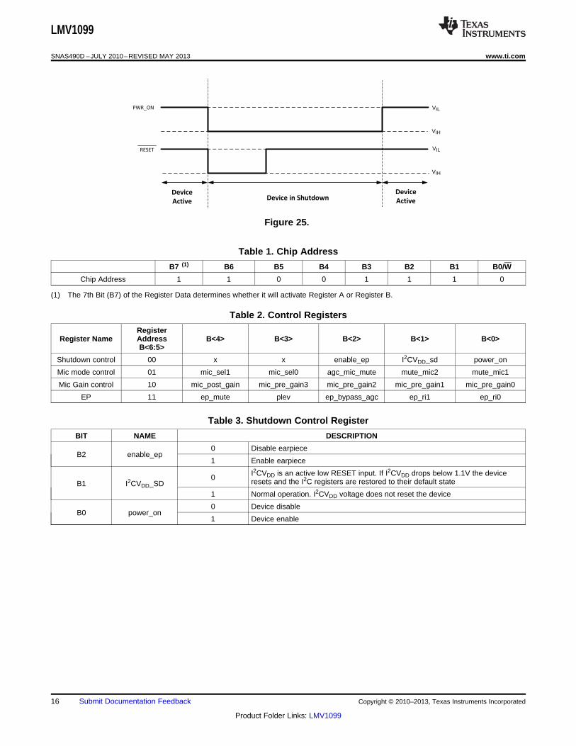
I2C RESET PIN
When the I2C RESET pin is pulled low, the device will go into shutdown and the Power_on bit (seeTable 2) in theshutdown control register will reset. The device will remain in shutdown until an I2C command brings the deviceout of shutdown (see timing diagram in Figure 25). This pin can be connected to the I2CVDD pin to preventundefined and unwanted state changes that may occur when the I2C supply voltage is cycled.
Copyright © 2010–2013, Texas Instruments Incorporated Submit Documentation Feedback 15
Product Folder Links: LMV1099
PWR_ON
VIH
VILRESET
Device
ActiveDevice in Shutdown
Device
Active
VIH
VIL
LMV1099
SNAS490D –JULY 2010–REVISED MAY 2013 www.ti.com
Figure 25.
Table 1. Chip Address
B7 (1) B6 B5 B4 B3 B2 B1 B0/W
Chip Address 1 1 0 0 1 1 1 0
(1) The 7th Bit (B7) of the Register Data determines whether it will activate Register A or Register B.
Table 2. Control Registers
RegisterRegister Name Address B<4> B<3> B<2> B<1> B<0>
B<6:5>
Shutdown control 00 x x enable_ep I2CVDD_sd power_on
Mic mode control 01 mic_sel1 mic_sel0 agc_mic_mute mute_mic2 mute_mic1
Mic Gain control 10 mic_post_gain mic_pre_gain3 mic_pre_gain2 mic_pre_gain1 mic_pre_gain0
EP 11 ep_mute plev ep_bypass_agc ep_ri1 ep_ri0
Table 3. Shutdown Control Register
BIT NAME DESCRIPTION
0 Disable earpieceB2 enable_ep
1 Enable earpiece
I2CVDD is an active low RESET input. If I2CVDD drops below 1.1V the device0 resets and the I2C registers are restored to their default stateB1 I2CVDD_SD1 Normal operation. I2CVDD voltage does not reset the device
0 Device disableB0 power_on
1 Device enable
16 Submit Documentation Feedback Copyright © 2010–2013, Texas Instruments Incorporated
Product Folder Links: LMV1099
LMV1099
www.ti.com SNAS490D –JULY 2010–REVISED MAY 2013
Table 4. LMV1099 Microphone Mode Control Register
BIT NAME DESCRIPTION
B4 B3
0 0 Noise canceling modemic_sel<4>B4:B3 0 1 Only mic1 enabled (pass through)mic_sel<3>
1 0 Only mic2 enabled (pass through)
1 1 (mic1+mic2)/2
0 mic1 & mic2 mute not allowedB2 agc_mic_mute
1 mic1 & mic2 mute allowed
0 mic2 onB1 mute_mic2 (1)
1 mic2 mute
0 mic1 onB0 mute_mic1 (1)
1 mic1 mute
(1) agc_mic_mute overrides mute_mic1 and mute_mic2
Table 5. LMV1099 Microphone Gain Control Register
BIT NAME DESCRIPTION
0 6dBB4 mic_post_gain
1 12dB
B3 B2 B1 B0
0 0 0 0 12dB
0 0 0 1 12dB
0 0 1 0 12dB
0 0 1 1 12dB
0 1 0 0 14dB
0 1 0 1 16dB
mic_pre_gain<3> 0 1 1 0 18dBmic_pre_gain<2>B3:B0 0 1 1 1 20dBmic_pre_gain<1>
1 0 0 0 22dBmic_pre_gain<0>
1 0 0 1 24dB
1 0 1 0 26dB
1 0 1 1 28dB
1 1 0 0 30dB
1 1 0 1 32dB
1 1 1 0 34dB
1 1 1 1 36dB
Table 6. LMV1099 Earpiece Control Register
BIT NAME DESCRIPTION
0 EP onB4 ep_mute
1 EP mute
3.6VP-P Earpiece Output Level0 (50mW with 32Ω load)B3 plev
4.1VP-P Earpiece Output Level1 (70mW with 32Ω load)
0 Normal operationB2 ep_bypass_agc Downlink SNR Enhancer Circuit bypassed (earpiece is1 still active)
Copyright © 2010–2013, Texas Instruments Incorporated Submit Documentation Feedback 17
Product Folder Links: LMV1099
LMV1099
SNAS490D –JULY 2010–REVISED MAY 2013 www.ti.com
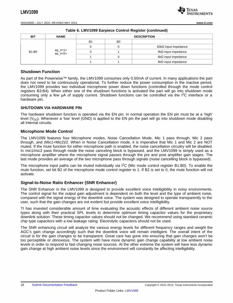
Table 6. LMV1099 Earpiece Control Register (continued)
BIT NAME DESCRIPTION
B1 B0
0 0 60kΩ input impedanceep_ri<1>B1:B0 0 1 9kΩ input impedanceep_ri<0>
1 0 6kΩ input impedance
1 1 6kΩ input impedance
Shutdown Function
As part of the Powerwise™ family, the LMV1099 consumes only 0.50mA of current. In many applications the partdoes not need to be continuously operational. To further reduce the power consumption in the inactive period,the LMV1099 provides two individual microphone power down functions (controlled through the mode controlregisters B3:B4). When either one of the shutdown functions is activated the part will go into shutdown modeconsuming only a few μA of supply current. Shutdown functions can be controlled via the I2C interface or ahardware pin.
SHUTDOWN VIA HARDWARE PIN
The hardware shutdown function is operated via the EN pin. In normal operation the EN pin must be at a ‘high’level (VDD). Whenever a ‘low’ level (GND) is applied to the EN pin the part will go into shutdown mode disablingall internal circuits.
Microphone Mode Control
The LMV1099 features four Microphone modes, Noise Cancellation Mode, Mic 1 pass through, Mic 2 passthrough, and (Mic1+Mic2)/2. When in Noise Cancellation mode, it is imperative that Mic 1 and Mic 2 are NOTmuted. If the mute function for either microphone path is enabled, the noise cancellation circuitry will be disabled.In mic1/mic2 pass through mode the noise canceling block is bypassed, and the LMV1099 is simply used as amicrophone amplifier where the microphone signal passes through the pre and post amplifier gain stages. Thelast mode provides an average of the two microphone pass through signals (noise cancelling block is bypassed).
The microphone input paths can be muted individually via I2C (Mic mode control register B1:B0). To enable themute function, set bit B2 of the microphone mode control register to 1. If B2 is set to 0, the mute function will notactivate.
Signal-to-Noise Ratio Enhancer (SNR Enhancer)
The SNR Enhancer in the LMV1099 is designed to provide excellent voice intelligibility in noisy environments.The control signal for the output gain adjustment is dependent on both the level and the type of ambient noise,compared with the signal energy of the downlink voice. The system was designed to operate transparently to theuser, such that the gain changes are not evident but provide excellent voice intelligibility.
TI has invested considerable amount of time evaluating the acoustic effects of different ambient noise sourcetypes along with their practical SPL levels to determine optimum timing capacitor values for the proprietarydownlink solution. These timing capacitor values should not be changed. We recommend using standard ceramicchip type capacitors with a low leakage rating. Electrolytic capacitors should not be used.
The SNR enhancing circuit will analyze the various energy levels for different frequency ranges and weight theAGC’s gain change accordingly such that the downlink voice will remain intelligent. The overall intent of thecircuit is for the gain changes to be transparent. Great care has gone into ensuring that gain changes won’t betoo perceptible or obnoxious. The system with have more dynamic gain change capability at low ambient noiselevels in order to respond to fast changing noise sources. At the other extreme the system will have less dynamicgain change at high ambient noise levels since the environment will constantly be affecting intelligibility.
18 Submit Documentation Feedback Copyright © 2010–2013, Texas Instruments Incorporated
Product Folder Links: LMV1099
LMV1099
www.ti.com SNAS490D –JULY 2010–REVISED MAY 2013
Earpiece Control Registers
OUTPUT POWER LIMIT (PLEV)
While TI has done extensive ambient SPL analysis, there will always be unusual circumstances that may causethe amplifier to be at its maximum 18dB setting. LMV1099 features an Output Voltage Limit function to limit theoutput power delivered to a speaker. When the SNR enhancer is active, the Output Voltage Limit works toprotect the loudspeaker in conditions where a large downlink input signal is present. The Output Voltage Limitcan be set to a selectable (3.6VP-P or 4.1VP-P) output level to avoid violating the maximum power limitation of thetransducer.
SNR ENHANCER BYPASS (EP_BYPASS_AGC)
The SNR enhancer can be bypassed by setting B4 of the Earpiece Control Register to 1. When the SNRenhancer is bypassed, the earpiece amplifier has a fixed 0dB gain.
EP_RI (INPUT IMPEDANCE)
The earpiece input of the LMV1099 features three input impedance options, this impedance in conjunction withthe input capacitor creates a high-pass filter. The three options provide various cutoff frequencies for the high-pass filter. Table 7 shows the respective cutoff frequencies for each of the input impedance options when using a68nF input capacitor.
Table 7. Input Impedance options
Input Impedance fC60kΩ 40Hz
9kΩ 260Hz
6kΩ 390Hz
Changing the input coupling capacitor will affect the filters –3dB point through the simple RC equation shownbelow:
f = 1 / 2πRC (1)
Microphone Placement
Because the LMV1099 is a microphone array Far Field Noise Reduction solution, proper microphone placementis critical for optimum performance. Two things need to be considered: The spacing between the twomicrophones and the position of the two microphones relative to near field source.
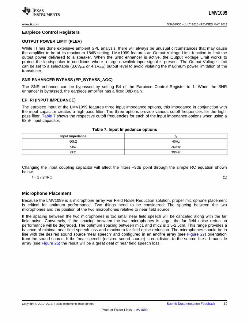
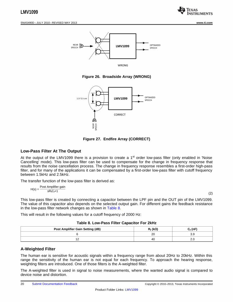
If the spacing between the two microphones is too small near field speech will be canceled along with the farfield noise. Conversely, if the spacing between the two microphones is large, the far field noise reductionperformance will be degraded. The optimum spacing between mic1 and mic2 is 1.5-2.5cm. This range provides abalance of minimal near field speech loss and maximum far field noise reduction. The microphones should be inline with the desired sound source 'near speech' and configured in an endfire array (see Figure 27) orientationfrom the sound source. If the 'near speech' (desired sound source) is equidistant to the source like a broadsidearray (see Figure 26) the result will be a great deal of near field speech loss.
Copyright © 2010–2013, Texas Instruments Incorporated Submit Documentation Feedback 19
Product Folder Links: LMV1099
H(s) = Post Amplifier gain
sRfCf+1
LMV1099
NE
AR
SP
EE
CH
CORRECT
1.5~2.5 cmOPTIMIZED
SPEECH
LMV1099NEAR
SPEECH
WRONG
OPTIMIZED
SPEECH
LMV1099
SNAS490D –JULY 2010–REVISED MAY 2013 www.ti.com
Figure 26. Broadside Array (WRONG)
Figure 27. Endfire Array (CORRECT)
Low-Pass Filter At The Output
At the output of the LMV1099 there is a provision to create a 1st order low-pass filter (only enabled in 'NoiseCancelling' mode). This low-pass filter can be used to compensate for the change in frequency response thatresults from the noise cancellation process. The change in frequency response resembles a first-order high-passfilter, and for many of the applications it can be compensated by a first-order low-pass filter with cutoff frequencybetween 1.5kHz and 2.5kHz.
The transfer function of the low-pass filter is derived as:
(2)
This low-pass filter is created by connecting a capacitor between the LPF pin and the OUT pin of the LMV1099.The value of this capacitor also depends on the selected output gain. For different gains the feedback resistancein the low-pass filter network changes as shown in Table 8.
This will result in the following values for a cutoff frequency of 2000 Hz:
Table 8. Low-Pass Filter Capacitor For 2kHz
Post Amplifier Gain Setting (dB) Rf (kΩ) Cf (nF)
6 20 3.9
12 40 2.0
A-Weighted Filter
The human ear is sensitive for acoustic signals within a frequency range from about 20Hz to 20kHz. Within thisrange the sensitivity of the human ear is not equal for each frequency. To approach the hearing response,weighting filters are introduced. One of those filters is the A-weighted filter.
The A-weighted filter is used in signal to noise measurements, where the wanted audio signal is compared todevice noise and distortion.
20 Submit Documentation Feedback Copyright © 2010–2013, Texas Instruments Incorporated
Product Folder Links: LMV1099
A-WEIGHTED FILTER
Mic2+
Mic2-
Mic1+
Mic1-
470 nF
470 nF
470 nF
470 nFOUT-
LPF
LMV1099
short
short
AC VoltmeterOUT+
10 100 1k 10k 100k
FREQUENCY (Hz)
-70
-60
-50
-40
-30
-20
-10
0
10
dBV
LMV1099
www.ti.com SNAS490D –JULY 2010–REVISED MAY 2013
The use of this filter improves the correlation of the measured values to the way these ratios are perceived bythe human ear.
Figure 28. A-Weighted Filter
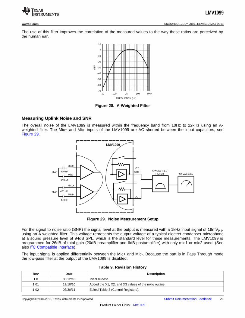
Measuring Uplink Noise and SNR
The overall noise of the LMV1099 is measured within the frequency band from 10Hz to 22kHz using an A-weighted filter. The Mic+ and Mic- inputs of the LMV1099 are AC shorted between the input capacitors, seeFigure 29.
Figure 29. Noise Measurement Setup
For the signal to noise ratio (SNR) the signal level at the output is measured with a 1kHz input signal of 18mVP-Pusing an A-weighted filter. This voltage represents the output voltage of a typical electret condenser microphoneat a sound pressure level of 94dB SPL, which is the standard level for these measurements. The LMV1099 isprogrammed for 26dB of total gain (20dB preamplifier and 6dB postamplifier) with only mic1 or mic2 used. (Seealso I2C Compatible Interface).
The input signal is applied differentially between the Mic+ and Mic-. Because the part is in Pass Through modethe low-pass filter at the output of the LMV1099 is disabled.
Table 9. Revision History
Rev Date Description
1.0 08/12/10 Initial release.
1.01 12/10/10 Added the X1, X2, and X3 values of the mktg outline.
1.02 03/30/11 Edited Table 3 (Control Registers).
Copyright © 2010–2013, Texas Instruments Incorporated Submit Documentation Feedback 21
Product Folder Links: LMV1099
LMV1099
SNAS490D –JULY 2010–REVISED MAY 2013 www.ti.com
Table 9. Revision History (continued)
Rev Date Description
D 05/02/13 Changed layout of National Data Sheet to TI format
22 Submit Documentation Feedback Copyright © 2010–2013, Texas Instruments Incorporated
Product Folder Links: LMV1099
PACKAGE OPTION ADDENDUM
www.ti.com 3-May-2013
Addendum-Page 1
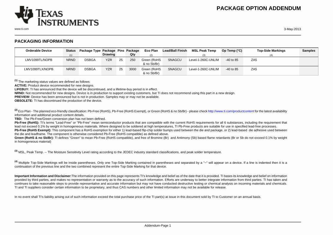
PACKAGING INFORMATION
Orderable Device Status(1)
Package Type PackageDrawing
Pins PackageQty
Eco Plan(2)
Lead/Ball Finish MSL Peak Temp(3)
Op Temp (°C) Top-Side Markings(4)
Samples
LMV1099TL/NOPB NRND DSBGA YZR 25 250 Green (RoHS& no Sb/Br)
SNAGCU Level-1-260C-UNLIM -40 to 85 ZA5
LMV1099TLX/NOPB NRND DSBGA YZR 25 3000 Green (RoHS& no Sb/Br)
SNAGCU Level-1-260C-UNLIM -40 to 85 ZA5
(1) The marketing status values are defined as follows:ACTIVE: Product device recommended for new designs.LIFEBUY: TI has announced that the device will be discontinued, and a lifetime-buy period is in effect.NRND: Not recommended for new designs. Device is in production to support existing customers, but TI does not recommend using this part in a new design.PREVIEW: Device has been announced but is not in production. Samples may or may not be available.OBSOLETE: TI has discontinued the production of the device.
(2) Eco Plan - The planned eco-friendly classification: Pb-Free (RoHS), Pb-Free (RoHS Exempt), or Green (RoHS & no Sb/Br) - please check http://www.ti.com/productcontent for the latest availabilityinformation and additional product content details.TBD: The Pb-Free/Green conversion plan has not been defined.Pb-Free (RoHS): TI's terms "Lead-Free" or "Pb-Free" mean semiconductor products that are compatible with the current RoHS requirements for all 6 substances, including the requirement thatlead not exceed 0.1% by weight in homogeneous materials. Where designed to be soldered at high temperatures, TI Pb-Free products are suitable for use in specified lead-free processes.Pb-Free (RoHS Exempt): This component has a RoHS exemption for either 1) lead-based flip-chip solder bumps used between the die and package, or 2) lead-based die adhesive used betweenthe die and leadframe. The component is otherwise considered Pb-Free (RoHS compatible) as defined above.Green (RoHS & no Sb/Br): TI defines "Green" to mean Pb-Free (RoHS compatible), and free of Bromine (Br) and Antimony (Sb) based flame retardants (Br or Sb do not exceed 0.1% by weightin homogeneous material)
(3) MSL, Peak Temp. -- The Moisture Sensitivity Level rating according to the JEDEC industry standard classifications, and peak solder temperature.
(4) Multiple Top-Side Markings will be inside parentheses. Only one Top-Side Marking contained in parentheses and separated by a "~" will appear on a device. If a line is indented then it is acontinuation of the previous line and the two combined represent the entire Top-Side Marking for that device.
Important Information and Disclaimer:The information provided on this page represents TI's knowledge and belief as of the date that it is provided. TI bases its knowledge and belief on informationprovided by third parties, and makes no representation or warranty as to the accuracy of such information. Efforts are underway to better integrate information from third parties. TI has taken andcontinues to take reasonable steps to provide representative and accurate information but may not have conducted destructive testing or chemical analysis on incoming materials and chemicals.TI and TI suppliers consider certain information to be proprietary, and thus CAS numbers and other limited information may not be available for release.
In no event shall TI's liability arising out of such information exceed the total purchase price of the TI part(s) at issue in this document sold by TI to Customer on an annual basis.
TAPE AND REEL INFORMATION
*All dimensions are nominal
Device PackageType
PackageDrawing
Pins SPQ ReelDiameter
(mm)
ReelWidth
W1 (mm)
A0(mm)
B0(mm)
K0(mm)
P1(mm)
W(mm)
Pin1Quadrant
LMV1099TL/NOPB DSBGA YZR 25 250 178.0 8.4 2.77 2.9 0.76 4.0 8.0 Q1
LMV1099TLX/NOPB DSBGA YZR 25 3000 178.0 8.4 2.77 2.9 0.76 4.0 8.0 Q1
PACKAGE MATERIALS INFORMATION
www.ti.com 8-May-2013
Pack Materials-Page 1
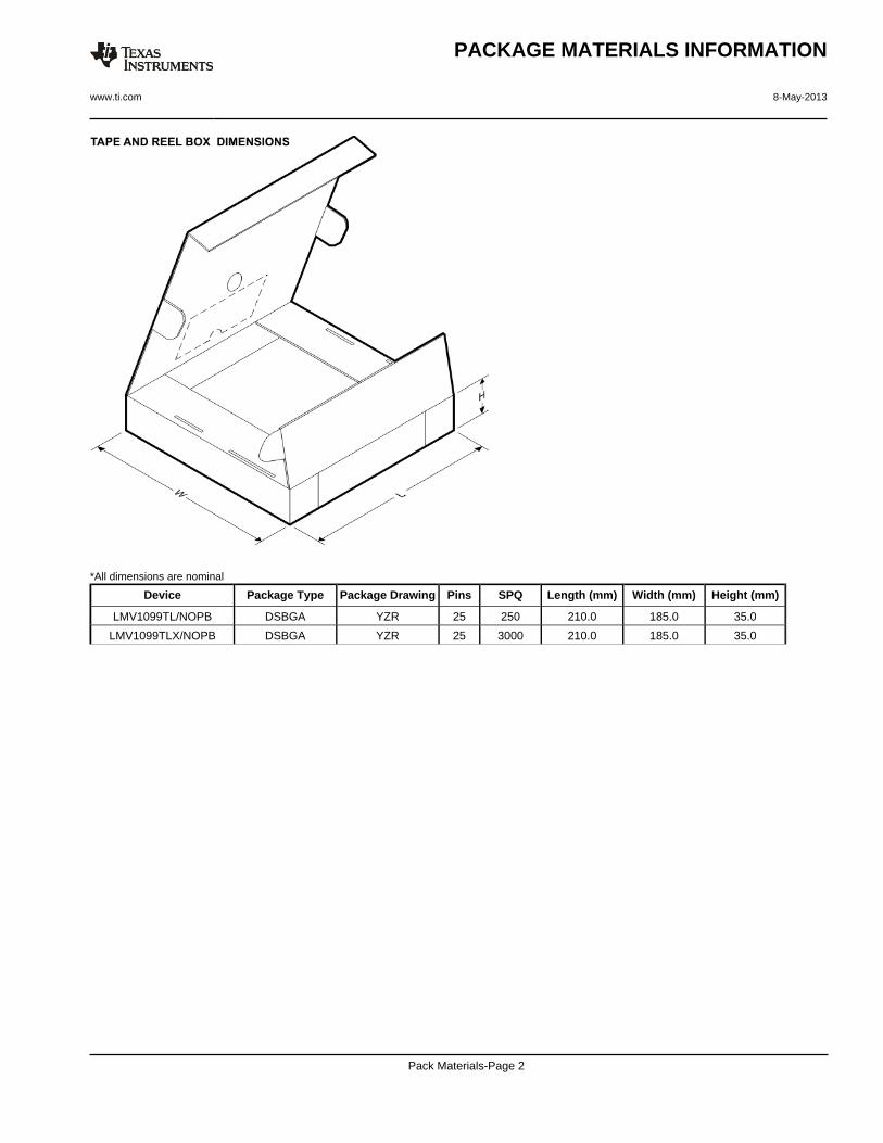
*All dimensions are nominal
Device Package Type Package Drawing Pins SPQ Length (mm) Width (mm) Height (mm)
LMV1099TL/NOPB DSBGA YZR 25 250 210.0 185.0 35.0
LMV1099TLX/NOPB DSBGA YZR 25 3000 210.0 185.0 35.0
PACKAGE MATERIALS INFORMATION
www.ti.com 8-May-2013
Pack Materials-Page 2
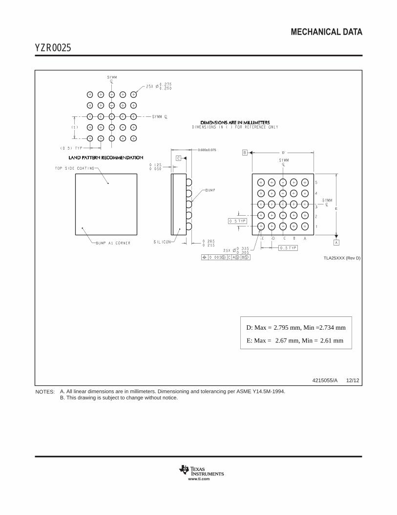
MECHANICAL DATA
YZR0025xxx
www.ti.com
TLA25XXX (Rev D)
0.600±0.075D
E
A. All linear dimensions are in millimeters. Dimensioning and tolerancing per ASME Y14.5M-1994.B. This drawing is subject to change without notice.
NOTES:
4215055/A 12/12
D: Max =
E: Max =
2.795 mm, Min =
2.67 mm, Min =
2.734 mm
2.61 mm
IMPORTANT NOTICE
Texas Instruments Incorporated (TI) reserves the right to make corrections, enhancements, improvements and other changes to itssemiconductor products and services per JESD46, latest issue, and to discontinue any product or service per JESD48, latest issue. Buyersshould obtain the latest relevant information before placing orders and should verify that such information is current and complete.TI’s published terms of sale for semiconductor products (http://www.ti.com/sc/docs/stdterms.htm) apply to the sale of packaged integratedcircuit products that TI has qualified and released to market. Additional terms may apply to the use or sale of other types of TI products andservices.Reproduction of significant portions of TI information in TI data sheets is permissible only if reproduction is without alteration and isaccompanied by all associated warranties, conditions, limitations, and notices. TI is not responsible or liable for such reproduceddocumentation. Information of third parties may be subject to additional restrictions. Resale of TI products or services with statementsdifferent from or beyond the parameters stated by TI for that product or service voids all express and any implied warranties for theassociated TI product or service and is an unfair and deceptive business practice. TI is not responsible or liable for any such statements.Buyers and others who are developing systems that incorporate TI products (collectively, “Designers”) understand and agree that Designersremain responsible for using their independent analysis, evaluation and judgment in designing their applications and that Designers havefull and exclusive responsibility to assure the safety of Designers' applications and compliance of their applications (and of all TI productsused in or for Designers’ applications) with all applicable regulations, laws and other applicable requirements. Designer represents that, withrespect to their applications, Designer has all the necessary expertise to create and implement safeguards that (1) anticipate dangerousconsequences of failures, (2) monitor failures and their consequences, and (3) lessen the likelihood of failures that might cause harm andtake appropriate actions. Designer agrees that prior to using or distributing any applications that include TI products, Designer willthoroughly test such applications and the functionality of such TI products as used in such applications.TI’s provision of technical, application or other design advice, quality characterization, reliability data or other services or information,including, but not limited to, reference designs and materials relating to evaluation modules, (collectively, “TI Resources”) are intended toassist designers who are developing applications that incorporate TI products; by downloading, accessing or using TI Resources in anyway, Designer (individually or, if Designer is acting on behalf of a company, Designer’s company) agrees to use any particular TI Resourcesolely for this purpose and subject to the terms of this Notice.TI’s provision of TI Resources does not expand or otherwise alter TI’s applicable published warranties or warranty disclaimers for TIproducts, and no additional obligations or liabilities arise from TI providing such TI Resources. TI reserves the right to make corrections,enhancements, improvements and other changes to its TI Resources. TI has not conducted any testing other than that specificallydescribed in the published documentation for a particular TI Resource.Designer is authorized to use, copy and modify any individual TI Resource only in connection with the development of applications thatinclude the TI product(s) identified in such TI Resource. NO OTHER LICENSE, EXPRESS OR IMPLIED, BY ESTOPPEL OR OTHERWISETO ANY OTHER TI INTELLECTUAL PROPERTY RIGHT, AND NO LICENSE TO ANY TECHNOLOGY OR INTELLECTUAL PROPERTYRIGHT OF TI OR ANY THIRD PARTY IS GRANTED HEREIN, including but not limited to any patent right, copyright, mask work right, orother intellectual property right relating to any combination, machine, or process in which TI products or services are used. Informationregarding or referencing third-party products or services does not constitute a license to use such products or services, or a warranty orendorsement thereof. Use of TI Resources may require a license from a third party under the patents or other intellectual property of thethird party, or a license from TI under the patents or other intellectual property of TI.TI RESOURCES ARE PROVIDED “AS IS” AND WITH ALL FAULTS. TI DISCLAIMS ALL OTHER WARRANTIES ORREPRESENTATIONS, EXPRESS OR IMPLIED, REGARDING RESOURCES OR USE THEREOF, INCLUDING BUT NOT LIMITED TOACCURACY OR COMPLETENESS, TITLE, ANY EPIDEMIC FAILURE WARRANTY AND ANY IMPLIED WARRANTIES OFMERCHANTABILITY, FITNESS FOR A PARTICULAR PURPOSE, AND NON-INFRINGEMENT OF ANY THIRD PARTY INTELLECTUALPROPERTY RIGHTS. TI SHALL NOT BE LIABLE FOR AND SHALL NOT DEFEND OR INDEMNIFY DESIGNER AGAINST ANY CLAIM,INCLUDING BUT NOT LIMITED TO ANY INFRINGEMENT CLAIM THAT RELATES TO OR IS BASED ON ANY COMBINATION OFPRODUCTS EVEN IF DESCRIBED IN TI RESOURCES OR OTHERWISE. IN NO EVENT SHALL TI BE LIABLE FOR ANY ACTUAL,DIRECT, SPECIAL, COLLATERAL, INDIRECT, PUNITIVE, INCIDENTAL, CONSEQUENTIAL OR EXEMPLARY DAMAGES INCONNECTION WITH OR ARISING OUT OF TI RESOURCES OR USE THEREOF, AND REGARDLESS OF WHETHER TI HAS BEENADVISED OF THE POSSIBILITY OF SUCH DAMAGES.Unless TI has explicitly designated an individual product as meeting the requirements of a particular industry standard (e.g., ISO/TS 16949and ISO 26262), TI is not responsible for any failure to meet such industry standard requirements.Where TI specifically promotes products as facilitating functional safety or as compliant with industry functional safety standards, suchproducts are intended to help enable customers to design and create their own applications that meet applicable functional safety standardsand requirements. Using products in an application does not by itself establish any safety features in the application. Designers mustensure compliance with safety-related requirements and standards applicable to their applications. Designer may not use any TI products inlife-critical medical equipment unless authorized officers of the parties have executed a special contract specifically governing such use.Life-critical medical equipment is medical equipment where failure of such equipment would cause serious bodily injury or death (e.g., lifesupport, pacemakers, defibrillators, heart pumps, neurostimulators, and implantables). Such equipment includes, without limitation, allmedical devices identified by the U.S. Food and Drug Administration as Class III devices and equivalent classifications outside the U.S.TI may expressly designate certain products as completing a particular qualification (e.g., Q100, Military Grade, or Enhanced Product).Designers agree that it has the necessary expertise to select the product with the appropriate qualification designation for their applicationsand that proper product selection is at Designers’ own risk. Designers are solely responsible for compliance with all legal and regulatoryrequirements in connection with such selection.Designer will fully indemnify TI and its representatives against any damages, costs, losses, and/or liabilities arising out of Designer’s non-compliance with the terms and provisions of this Notice.
Mailing Address: Texas Instruments, Post Office Box 655303, Dallas, Texas 75265Copyright © 2017, Texas Instruments Incorporated


![1 Downlink and Uplink Cell Association with …arXiv:1601.05281v1 [cs.IT] 20 Jan 2016 1 Downlink and Uplink Cell Association with Traditional Macrocells and Millimeter Wave Small Cells](https://img.dokumen.tips/doc/110x75/5e95bd0c0c147f2995470045/1-downlink-and-uplink-cell-association-with-arxiv160105281v1-csit-20-jan-2016.jpg)


![10 GSM BSS Network KPI (Uplink-Downlink Balance) Optimization Manual[1].Doc](https://img.dokumen.tips/doc/110x75/545a3905af795998788b5b03/10-gsm-bss-network-kpi-uplink-downlink-balance-optimization-manual1doc.jpg)


![10 gsm bss network kpi (uplink downlink balance) optimization manual[1].doc](https://img.dokumen.tips/doc/110x75/558ec7491a28ab66628b474b/10-gsm-bss-network-kpi-uplink-downlink-balance-optimization-manual1doc-558f343a2e921.jpg)

![10 GSM BSS Network KPI (Uplink-Downlink Balance) Optimization Manual[1].doc.doc](https://img.dokumen.tips/doc/110x75/55cf9bb1550346d033a705c6/10-gsm-bss-network-kpi-uplink-downlink-balance-optimization-manual1docdoc.jpg)