Embed Size (px)
Citation preview

Kenneth R. Laker, 14Sep08 (based on Lab Into by Phillip V. Loprsti, 2006)
University of Pennsylvania Moore School of Electrical Engineering
ESE319 Electronic Circuits - Modeling and Measurement Techniques
1. Introduction. Students are often frustrated in their attempts to execute laboratory experiments in electronics courses. Their experimental results often do not bear much resemblance to what they expect to see based on the theory they learn in lecture and from their textbooks. Most of the difficulties they encounter exist because conventional texts and classroom discussions assume the ideal behavior of typical circuits. These instructional sources do not mention several important considerations that have a striking effect on the outcome of any attempted experimental procedure. Physical phenomena that tend to corrupt experimental results include:
• Circuit loading caused by the insertion of laboratory instrument measurement probes. • Parasitic circuit elements inserted in the ideal circuit. In our case, the principal source is the ProtoBoard interconnect system we use. • Noise generated by external sources and induced in the circuit wiring.
If we were able to satisfy the following conditions:
• Input devices - function generators, for example - have zero output impedance. • Output measuring instruments - oscilloscopes, voltmeters, etc. - have infinite input impedance. • Connecting wires are of zero length. • All sources of electrical energy production and consumption - radio transmitters, fluorescent lighting fixtures, electric motors, etc., are turned off during the course of our experiments,
Then our experimental results consistently would agree much better with textbook predictions. Unfortunately, such is not the case and we must conduct experiments in a less than ideal real-world environment. Many, but not all, of these problems can be eliminated by following some simple "rules of thumb" when constructing a circuit, but much experience and insight into circuit behavior is required to make high performance circuits work properly. Circuit design engineers - particularly analog designers - spend years learning how to deal intelligently with these idiosyncrasies of circuit design and layout. Although one cannot hope to capture the knowledge of an experienced designer in a few pages, the following material hopefully will assist students in completing electronics laboratory experiments with a high degree of success. 2. Organization. The following sections will address the physical limitations of electronics experimental setups in the following order:
• First, we will examine techniques for modeling circuit interconnect wiring and the basic passive circuit components: resistors, capacitors, and inductors. Each length of wire, including the leads on resistors, inductors, and capacitors, has parasitic (undesired)

Kenneth R. Laker, 14Sep08 (based on Lab Into by Phillip V. Loprsti, 2006)
2
inductance and resistance. These parasitic effects may be negligible or significant, depending on the impedance level of the rest of the circuit and on the circuit's operating frequency. Additional parasitic effects exist as capacitance or mutual inductance between adjacent wires, or as a capacitance between a wire and a conducting ground plane. • Next, we will discuss the modeling of coaxial cable. Coax is used generally to connect signal sources, such as function generators, and measuring instruments - multimeters and oscilloscopes - to the circuit being evaluated and tested. • Then we will cover circuit models for typical function generators and oscilloscopes and discuss how these instruments interact with the circuit under test. • Next, we will show several ways in which noise signals can enter the circuit under test and corrupt circuit performance. • Finally, we will illustrate how to derive detailed models for several simple circuits, illustrating how certain parasitic effects may have negligible effect on the circuit under test in some instances and have significant effect in others.
2. Circuit models for the laboratory. 2.1 Interconnect wiring. Resistance describes the relationship between voltage across and current through an electrical conductor. Inductance, on the other hand, is a measure of the relationship between current flow and the magnetic flux resulting from that current. Every current-carrying wire has resistance and inductance and, as a consequence, every wire exhibits a certain amount of frequency-dependent impedance due to current flow. Since interconnecting wires in a circuit ideally are assumed to be impedance-free, the undesired circuit elements - resistance and inductance - are called parasitics.
Rlead
L lead
Fig. 2.1 Interconnect lead model
Accurate formulas for computing the inductance of a conductor are complex, but one sufficiently exact for our purposes is given as:
L(µH ) = .002 l 2.5 log10 4l
d! 0.75"
# $
%
& '
(
) * +
, - (2.1)
Where l is the length in cm. of a straight piece of wire and d is its diameter in cm (2.54 cm. = 1 inch and 1 mil = 0.001 in.). Table 2.1 illustrates the inductance in microhenries of one foot and one meter of wire for several common wire gauges used for circuit interconnect. The resistance of the wire also is tabulated.

Kenneth R. Laker, 14Sep08 (based on Lab Into by Phillip V. Loprsti, 2006)
3
Wire Wire Wire Inductance Inductance Resistance Resistance
gauge diameter diameter per foot per meter per foot per meter
AWG mils cm. uH. uH. Ohms Ohms
18.00 40.30 0.10 0.47 1.54 0.006 0.020
20.00 28.50 0.07 0.49 1.61 0.010 0.033
22.00 25.30 0.06 0.50 1.64 0.016 0.052
24.00 20.10 0.05 0.51 1.69 0.026 0.085
26.00 15.90 0.04 0.53 1.74 0.041 0.135
28.00 12.60 0.03 0.55 1.79 0.065 0.213
Table 2.1 Copper wire inductance and resistance. Interconnect wiring resistance usually can be ignored since its impedance usually is much less than other impedances in series with the wire. Parasitic inductance is another matter, however, and its effect cannot be neglected at higher frequencies. The inductive reactance ( j!Lr ) of a one meter length of 18 gauge wire is tabulated in Table 2.2. The reader easily can calculate the reactance of other wire gauges and of other lengths using proportionality and linearity arguments. As a rough estimate, all of the common wire gauges can be considered to have the same inductance per unit length as 18 gauge wire. All inductive reactance estimates can be obtained by multiplying the reactance of a 1 meter length by the actual length of the wire in meters (or fractions thereof).
Frequency Frequency Reactance
KHz. Kradians/sec. Ohms
0.01 0.06 0.0001
0.1 0.63 0.0010
1 6.28 0.0097
10 62.83 0.0966
100 628.32 0.9662
1000 6283.19 9.6625
10000 62831.85 96.6248
Table 2.2 Inductive reactance of 1 meter of 18 gauge wire. 2.2 Resistors. Ideal resistors exhibit only resistance. Physical resistors, however, have associated parasitic inductance, since they require a finite length current-conducting path. A good high frequency resistor model also includes a parasitic capacitor across the resistor body. At a high enough frequency, this seemingly small capacitor will have a smaller reactance than the resistance of the resistor and most current flow will be through the terminal-to-terminal capacitance of the resistor, rather than through its resistive material. This capacitance typically is about 0.5 pF. That corresponds to a capacitive reactance of about 31.8 kΩ at 10 MHz and 318 MΩ at 1 kHz. We shall not have to consider this parasitic capacitance unless the capacitive reactance is less than 10 times the resistance of our physical resistor at the highest operating frequency of our circuit. The shunting (parallel) capacitance of a 1 kΩ resistor operating at 10 MHz, for example, can be ignored, but not that of a 10 kΩ one used at 10 MHz. A resistor's lead inductance is quite small and usually can be neglected, since the leads will generally be less than an inch in length. Only at very high frequencies

Kenneth R. Laker, 14Sep08 (based on Lab Into by Phillip V. Loprsti, 2006)
4
- RF frequencies - will we need to consider resistor lead inductance. A detailed circuit model for a resistor is shown in Fig. 2.2. We will discuss some useful "rules-of-thumb" for circuit simplifications of this type later in this document
R Lr
Cr
Fig. 2.2 High frequency resistor model. 2.3 Capacitors. Ideal capacitors are purely reactive - conduction occurs via a displacement current across the capacitor dielectric. As is the case for resistors, however, capacitors have parasitics - series resistance, shunt resistance, and series inductance. Inductance and resistance exist because of the finite conducting path. Additional resistance effects due to energy losses in the capacitor dielectric also must be considered in some cases. All capacitors also have a small amount of leakage current - conductive current that flows directly through its less-than-perfectly insulating dielectric. A detailed model for a physical capacitor is shown in Fig. 2.3.
R cp
Lc
CR cs
Fig. 2.3 High frequency capacitor model. Perhaps the most serious problem occurring with capacitors is the interaction between the capacitor's capacitance and its series inductance. If we neglect the large leakage resistance, Rcp , the complex impedance of a physical capacitor is
ZC = Rcs + j !Lc "1
!C#
$ %
&
' ( (2.2)
This element combination will series resonate at the frequency where: !L
c=1
!C (2.3)

Kenneth R. Laker, 14Sep08 (based on Lab Into by Phillip V. Loprsti, 2006)
5
At this frequency, the capacitor impedance will attain a minimum value equal to its small series resistance. Above its resonant frequency, the capacitor impedance will increase - it is now behaving like an inductor! In most of our applications, capacitors are used either to block dc or to provide a low impedance path for signal currents. In any case, they are supposed to have negligible impedance at all frequencies of interest. If, however, one tries for "overkill" and uses a much larger value capacitor in a circuit than necessary, series resonance may occur and the super size capacitor chosen for its super low impedance may actually have a rather high impedance at higher operating frequencies. For example, if we decide to use a 100 µF capacitor in a situation where we want an effective "short-circuit," and the capacitor's lead inductance is 0.01 µH, a self resonance will occur at about 160 kHz and the impedance of the "capacitor" will increase above that frequency since the inductive reactance of the leads will be greater than the capacitive reactance of the capacitor. 2.4 Inductors. It is difficult to construct physical inductors that do not have significant associated parasitics. Series resistance and shunt capacitance effects are the most common. It is even more difficult to obtain a circuit model that will be accurate over a wide frequency range. Fortunately, the only inductance we usually will have to deal is the parasitic inductance of circuit leads, resistors, or capacitors. 3. Coaxial cable. Coaxial cable ("coax") usually is used to connect test instruments to a circuit under test. When properly used, coax has the ability to minimize noise pickup from external sources and to prevent the test leads from radiating undesired signals into our test environment. Coax consists of an inner conducting wire surrounded by an outside metallic sheath. The sheath forms the return path for the current flowing down the inner wire (Fig. 3.1). An insulating material chosen for its dielectric properties separates the two conductors. If equal currents flow in opposite directions on the inner conductor and on the outer shell, i.e., if the line currents are balanced, the electromagnetic fields caused by the current are confined within the coax.
Insulating jacket Outer conducting shell
Dielectric Inner conductor
Fig. 3.1 Coaxial cable cross-section. Since coax is composed of current-carrying conductors, it has a well-defined inductance per unit length. The cable conductors are held in close proximity by the dielectric, thus coax also has a well-defined capacitance per unit length. The line inductance and capacitance are intermingled - distributed - along the length of the line and a precise treatment of the behavior of the line needs to take the distributed nature of the line parameters into account. Coax is classified as a transmission

Kenneth R. Laker, 14Sep08 (based on Lab Into by Phillip V. Loprsti, 2006)
6
line and its properties are described by its characteristic impedance. The characteristic impedance of coax is defined as the geometric mean (square root) of the product of its per-unit-length inductive reactance and its pre-unit-length capacitive reactance.
Zo=
!L
!C=
L
C (3.1)
The most common value for Z
o is 50 ohms and a typical coax capacitance is 30 pF per foot. It then
follows that this "fifty-ohm" coax has a per-unit inductance of: L = CZ
o
2= 30 !10
"12! 50
2= 0.075µH per foot (3.2)
The cable also has resistance, but this resistance usually is small enough to be ignored. For our purposes, we can assume that coax is a "lossless" (resistance-less) transmission line. A theoretical treatment of the behavior of transmission lines is beyond the scope of this discussion, but we will make several observations about their properties:
• If a transmission line is terminated in its characteristic impedance, the impedance across its input terminals will equal its characteristic impedance, regardless of the length of the line, even though it be many wavelengths long. • In a properly terminated line, the signal at the line termination will "look like" the signal at its input, delayed by a time interval proportional to the length of the line. • If coax is terminated in other than its characteristic impedance, standing waves will appear across the line and the impedance at the input terminals of the coax will not equal its terminating impedance, but will vary, depending on the length of the line in electrical wavelengths. • As an extreme example, a line whose termination is an open circuit will have an input impedance that varies periodically from infinity to zero, depending on the length of the line and on its excitation frequency. A short-circuited line will have an input impedance that also varies periodically from zero to infinity as its excitation frequency, or its length, changes. • A calculated length of transmission line, with either a short-circuit or open-circuit termination, is called a stub. By selecting a proper stub length, we theoretically can obtain any desired circuit impedance at any desired frequency at the line input nodes. We can make a transmission line stub look like a capacitor or an inductor with reactance of any value we want. Unfortunately, stubs are useful only at short wavelength radio frequencies. The stub lengths required for use in the kilohertz signal range would be far too long to be practical.
For our purposes, any length of coax we use in the lab will be "short" - a small fraction of a wavelength of the signal applied to it. If the coax is terminated in a "large" impedance, such as an oscilloscope input, we can approximate the piece of coax as a capacitor whose capacitance is equal to the length of the coax times its per-unit length capacitance. If the coax is terminated in a "small" valued impedance- seldom the case - we can approximate it as an inductor whose inductance equals the length of the coax times its per unit length inductance. The inductance is split between the inner and the outer conductors. 4. Function generator characteristics.
Kenneth R. Laker, 14Sep08 (based on Lab Into by Phillip V. Loprsti, 2006)
7
A function generator or arbitrary waveform generator is generally a well-behaved instrument in most laboratory setups. Typically, it has a switch-selectable choice of sine, square wave, or triangular output waveshape, and the generator frequency and output amplitude can be varied over a wide range. A circuit model for a generic function generator consists of an ideal voltage source representing the output waveshape at the desired voltage and a series resistance representing the non-zero output impedance of the generator. The function generator output impedance typically is 50 Ω or 600 Ω for low frequency generators and 50 Ω (to match coaxial cable) for radio frequency and microwave generators. A model for the generic function generator is shown in Fig. 4.1.
R
V
Power line ground
Earth
g
g
Coax connector
Fig. 4.1. Function generator circuit model
The output terminals of the generator are usually brought to a coaxial cable connector and the generator is connected to the circuit using a length of 50 Ω coaxial cable. Note that the function generator "low" terminal is connected to earth over the lab power line wiring. As we will soon see, this ground connection - necessary for safety reasons - can cause problems, introducing noise into our circuit measurements through "ground loop" effects. If we assume that the input impedance of the circuit to which the generator is connected is considerably higher than 50 Ω, the coax can be represented as a capacitor connected across the function generator terminals. A one meter length of coax has capacitance of about 100 pF therefore its reactance at 1 MHz is:
XC=
1
2!106"100 "10
#12=10
4
2!= 1592$ (4.1)
and at 10 MHz it is 159.2 Ω. The coax impedance exerts a significant load on the function generator at higher frequencies and its effect must be compensated. This frequency-dependent loading is not a problem if the function generator is producing pure sine waves - a 'scope probe could be connected across the circuit connection points of the function generator and the generator amplitude adjusted for the correct voltage at the probe. For best accuracy, the probe should be kept connected for the duration of the measurement, since its high frequency input impedance may be low enough to load the function generator and its removal may cause a significant change in the voltage applied to the circuit under test.

Kenneth R. Laker, 14Sep08 (based on Lab Into by Phillip V. Loprsti, 2006)
8
Problems occur if we try to drive our circuit with a high frequency square wave or triangular wave. Recall from Fourier series theory that these waveforms can be represented as a sum of harmonically-related sinusoids. Unfortunately, the load on the function generator is frequency-dependent so the harmonic content of a square wave, for example, will not be preserved and the waveform presented to the circuit will be distorted. A simple way to handle this is to terminate the coax with a 47 or 51 Ω resistor - resistance values suitably close to the characteristic impedance of the coax - and connect the coax- resistor junction to the circuit under test (Fig. 4.2). Recall from the discussion of the properties of coaxial cable that if the coax termination matches its characteristic impedance, the impedance across its input terminals - those connected to the function generator will equal the characteristic impedance at all frequencies. Loading thus is the same at all frequencies and the signal waveshape at the circuit will be the same as that generated by the function generator, but delayed in time. Also, a function generator with 50 Ω output impedance at the end of the terminated coax will look like a voltage source of 1/2 the open-circuit source value with a 25 Ω Thevinen equivalent output impedance. Since the circuit input impedance also is connected across the coax, this model will hold only if it is much greater than 50 Ω at all frequencies of interest.
R
V
Power line ground
Earth
g
g
47 Ohms
50 Ohm CoaxFunction generator
Circuit ground
Circuit input
Coax connector
Fig. 4.2 Termination for frequency independent coax loading. 5. Oscilloscope characteristics. The most important measuring instrument that you will use in electronics is the oscilloscope. Often the only way that you can observe the performance of your circuit is to display the time waveforms existing at different layout nodes. Connecting an instrument to your circuit, however, is equivalent to connecting more circuit elements across the measurement points. A schematic of the input terminals of a typical oscilloscope is shown in Fig. 5.1

Kenneth R. Laker, 14Sep08 (based on Lab Into by Phillip V. Loprsti, 2006)
9
C = 20 pF R =1 Mohm
Scope power cableground wire
EarthPower system ground
Coax Connector
To other circuits on this line
Fig. 5.1 Oscilloscope input circuit
There are two important features to note about the oscilloscope input connection:
• The 'scope input impedance has a maximum value of 1 MΩ at dc and decreases with increasing frequency since the reactance of the parallel capacitor decreases with frequency. Decreasing input impedance means that the load that the oscilloscope places on the circuit under test increases as the circuit operating frequency increases. Because of oscilloscope loading, what may be an accurate measurement at 1 kHz may be a very poor one at 10 MHz! • The shell of the 'scope connector is tied to earth through the 'scope power line connection. This path to earth is shared with any other electrical device that happens to be connected to the same circuit. Ground paths shared with operating electrical devices - fluorescent lights, for example - are a common source of the noise that appears in an experimental circuit.
5.a. Oscilloscope input interface. We need to connect our oscilloscope to the nodes that we wish to observe. This connection requires that a conductor run between the 'scope input and the node. The usual approach is to use a piece of coaxial cable with a coaxial connector on one end and clip leads on the other. One clip is connected to the coax shield, which is connected to earth. The other is connected to the coax center connector. The voltage we will observe is that between the center connector lead and the grounded lead, which should be connected to the common ("ground") node of the circuit under test. Unfortunately, this connecting cable introduces additional capacitance in parallel with the input capacitance of the oscilloscope. Coaxial cable of this type typically has a capacitance of about 30 pF per foot, so a three-foot cable would increase the effective capacitance connected across the measurement points to over 100 pF. Table 5.1 illustrates the oscilloscope input impedance variation with frequency using this type of connection, i.e. assuming 100 pF total capacitance.

Kenneth R. Laker, 14Sep08 (based on Lab Into by Phillip V. Loprsti, 2006)
10
Frequency Frequency Input Input Impedance
Rad/sec Hz reactance resistance magnitude
1.00 0.16 1.00E+10 1.00E+06 1.00E+06
10.00 1.59 1.00E+09 1.00E+06 1.00E+06
100.00 15.92 1.00E+08 1.00E+06 1.00E+06
1,000.00 159.15 1.00E+07 1.00E+06 9.95E+05
10,000.00 1,591.55 1.00E+06 1.00E+06 7.07E+05
100,000.00 15,915.49 1.00E+05 1.00E+06 9.95E+04
1,000,000.00 159,154.94 1.00E+04 1.00E+06 1.00E+04
10,000,000.00 1,591,549.43 1.00E+03 1.00E+06 1.00E+03
Table 5.1. Oscilloscope input impedance variation with frequency.
Note that for frequencies below about 1,000 radians per second, or 159 Hz. the input impedance can be approximated reasonably as a resistance of 1 MΩ. Above about 100,000 radians per second, 15.91 kHz., the input connection to the 'scope can be approximated closely as purely capacitive and the 'scope input impedance decreases rapidly with frequency. 5.b Attenuating oscilloscope probes. The common approach taken to reduce oscilloscope loading is to use special probes to connect the 'scope input to the circuit nodes. Fig. 5.2 represents a "10x probe" attached to an oscilloscope input connector. A 10x probe attenuates the input voltage at the probe tip by a factor of 10 at the 'scope input connector. Thus, the voltage seen at the 'scope input is only 1/10 of the input voltage. Why intentionally attenuate the voltage we wish to observe? Because it increases the impedance across the test nodes by a factor of 10!
R =1 Mohm
Coax
C = 20 pF
Oscilloscope Input
CableCapacitance = 80 pF
Probe Tip
Probe Body
Ground Clip
R = 9 Mohm
C = 12 pFp
p
s
sC
c
Fig. 5.2 10x probe connected to oscilloscope input.
Modeling of the probe action is based on the voltage divider action of the series combination of two impedances, each consisting of a capacitor and resistor in parallel. The first parallel circuit consists of the 'scope input resistance and a parallel combination of the cable capacitance and the 'scope input capacitance. We have a 100 pF equivalent capacitance in parallel with a 1 MΩ resistor:
Zs+ c
=
Rs
1
sCs+ c
Rs+
1
sCs+ c
=Rs
sRsCs +c
+1 (5.1)

Kenneth R. Laker, 14Sep08 (based on Lab Into by Phillip V. Loprsti, 2006)
11
We define the time constant of the probe-plus-cable combination as: !
s +c= R
sCs +c
(5.2) The probe contains a comparable parallel circuit consisting of the probe resistor and an adjustable capacitor. The impedance of the probe is:
Zp =
Rp
1
sCp
Rp +1
sCp
=Rp
sRpCp +1 (5.3)
and the probe time constant is: ! p = RpCp (5.4) The parallel impedance pairs form a simple voltage divider leading to a 'scope voltage of: Vscope =
Zs + c
Zs +c + ZpVin (5.5)
or:
Vscope =
Rs
s! s +c +1
Rs
s! s +c +1+
Rp
s! p +1
Vin (5.6)
If the probe capacitor is adjusted properly: RpCp = RsCs+ c (5.7) and ! p = ! s+ c (5.8) With this time constant match and the resultant cancellation of the s! +1 terms in Eq. (5.6), the voltage divider ratio becomes: Vscope =
Rs
Rs + RpVin =
1
1 +Rp
Rs
Vin =1
1+ 9Vin =
1
10Vin (5.9)
Since RpCp = RsCs+ c (5.10) we have:

Kenneth R. Laker, 14Sep08 (based on Lab Into by Phillip V. Loprsti, 2006)
12
Rp
Rs=Cs+ c
Cp
(5.11)
If we then substitute for the resistance ratio in Eq. (5.9), we obtain an equivalent expression for the voltage divider:
Vscope =1
1 +Cs +c
Cp
Vin =Cp
Cp + Cs +cVin (5.12)
The voltage divider output is equal to one-tenth of the probe input voltage and is independent of the frequency of the input signal. This type of circuit is called an allpass filter, since its output voltage magnitude is independent of frequency. Another important characteristic of the probe is its effect on the 'scope input impedance. The input impedance is formed by a series combination of two parallel RC circuits with equal time constants:
Zin =Rs
s! s+ c +1+
Rp
s! p +1=Rs + Rp
s! +1 (5.13)
Note that the common time constant is the same as the time constant we had obtained previously for the 'scope connected directly to the test points via a piece of coaxial cable. We leave it to the reader to verify that an equivalent expression for the input impedance time constant is:
! = (Rs + Rp )CpCs+ c
Cp + Cs+ c
= (Rs + Rp)Cser (5.14)
As far as the input impedance is concerned, the probe appears as a combination of two series resistors connected in parallel with two series capacitors. The "real" mid-point connection of the resistors and capacitors is effectively "opened" since the mid-point voltage drop across the resistors equals that across the capacitors at all frequencies and no current flows through the mid-point connection. The probe equivalent series resistance is 10 MΩ and its equivalent series capacitance is: Cser =
!
Rs + Rp=RsCs +c
Rs + Rp=1
10Cs+ c
(5.15)
Thus, the input resistance is ten times the basic oscilloscope input resistance, the equivalent capacitance is one-tenth the oscilloscope plus coax input capacitance, and the probe increases the measurement input impedance by an order of magnitude. Unfortunately, the oscilloscope still may have insufficient input impedance for circuit measurements at high frequencies. Table 5.2 shows the input impedance variation with frequency of this typical 10x probe.
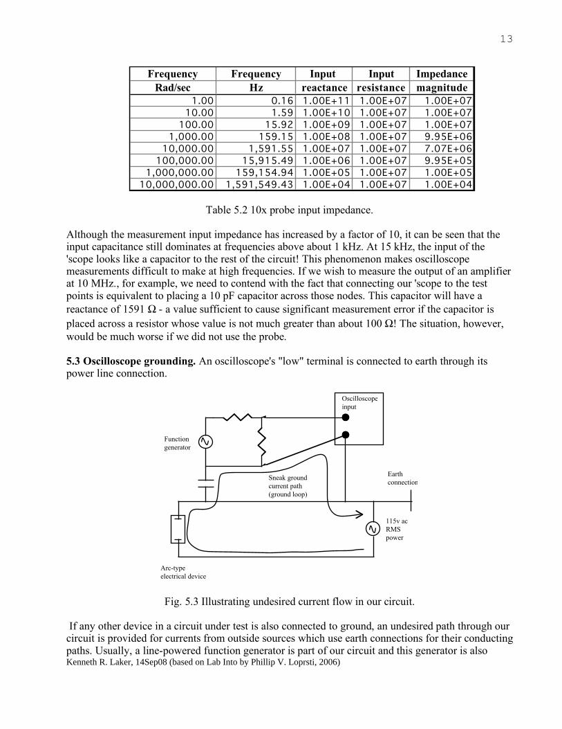
Kenneth R. Laker, 14Sep08 (based on Lab Into by Phillip V. Loprsti, 2006)
13
Frequency Frequency Input Input Impedance
Rad/sec Hz reactance resistance magnitude
1.00 0.16 1.00E+11 1.00E+07 1.00E+07
10.00 1.59 1.00E+10 1.00E+07 1.00E+07
100.00 15.92 1.00E+09 1.00E+07 1.00E+07
1,000.00 159.15 1.00E+08 1.00E+07 9.95E+06
10,000.00 1,591.55 1.00E+07 1.00E+07 7.07E+06
100,000.00 15,915.49 1.00E+06 1.00E+07 9.95E+05
1,000,000.00 159,154.94 1.00E+05 1.00E+07 1.00E+05
10,000,000.00 1,591,549.43 1.00E+04 1.00E+07 1.00E+04
Table 5.2 10x probe input impedance.
Although the measurement input impedance has increased by a factor of 10, it can be seen that the input capacitance still dominates at frequencies above about 1 kHz. At 15 kHz, the input of the 'scope looks like a capacitor to the rest of the circuit! This phenomenon makes oscilloscope measurements difficult to make at high frequencies. If we wish to measure the output of an amplifier at 10 MHz., for example, we need to contend with the fact that connecting our 'scope to the test points is equivalent to placing a 10 pF capacitor across those nodes. This capacitor will have a reactance of 1591 Ω - a value sufficient to cause significant measurement error if the capacitor is placed across a resistor whose value is not much greater than about 100 Ω! The situation, however, would be much worse if we did not use the probe. 5.3 Oscilloscope grounding. An oscilloscope's "low" terminal is connected to earth through its power line connection.
Oscilloscope
input
Function
generator
115v ac
RMS
power
Arc-type
electrical device
Earth
connectionSneak ground
current path
(ground loop)
Fig. 5.3 Illustrating undesired current flow in our circuit. If any other device in a circuit under test is also connected to ground, an undesired path through our circuit is provided for currents from outside sources which use earth connections for their conducting paths. Usually, a line-powered function generator is part of our circuit and this generator is also

Kenneth R. Laker, 14Sep08 (based on Lab Into by Phillip V. Loprsti, 2006)
14
connected to earth through its power line connector. A simple circuit illustrating a potential problem source is shown in Fig. 5.3. The loop created by this connection also creates an opportunity for other sources to couple magnetically with our circuit. Ground loops are common sources of 60 Hz power line noise in our measurements. Ground loops also act as radio antennas and will pick up quite strong RF signals from nearby radio transmitters. The best way to minimize ground loop effects is minimize the length of the path between the instrument power line ground and circuit measurement ground connections:
• Connect the 'scope probe ground clip to the circuit node closest to the function generator input "low" terminal. • Plug both instruments into the same ac outlet (Fig. 5.4).
Oscilloscope
input
Function
generator
115v ac
RMS
power
Arc-type
electrical device
Earth
connection
Minimize
noise voltage
drop
Shorten path to
minimize impedance
to noise current
Fig. 5.4 Illustrating ground loop effect minimization. Actually, it's good form, where possible, to connect all off-ground power supply voltage leads to one point on the circuit board and all power and circuit "ground" leads to another single point. All ground lead paths should be as short as possible and connections are made to the 'scope, the function generator, and the power supply ground terminal at this point. All powered devices, should have their off-ground power supply potential points also run to a common point from which a connection is made to the power supply. This approach minimizes the possibility that signal currents flowing through power leads from different parts of the circuit will, through impedance drops in the leads, interact with other parts of the circuit. It also minimizes the size of the ground loop around our experimental circuit.