Embed Size (px)
Citation preview
ESE319 Introduction to Microelectronics
12009 Kenneth R. Laker, updated 25Sep12 KRL
BJT Biasing Cont. & Small Signal Model
● Bias Design Example using “1/3, 1/3, 1/3 Rule”● Small Signal BJT Models● Small Signal Analysis
ESE319 Introduction to Microelectronics
22009 Kenneth R. Laker, updated 25Sep12 KRL
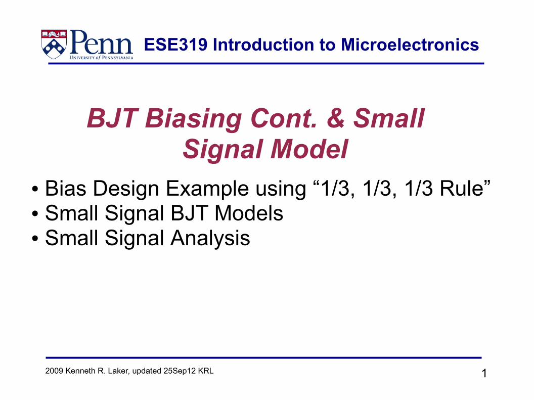
Emitter Feedback Bias Design
Two power supply version Single power supply version
I1 I
C
IE
IB
VB
RC
RE
RB
VCC
RC
RE
R1
R2
V B=R2
R1R2V CC
RB=R1 R2
R1R2R1=RB
V CC
V B
R2=R1
V B
V CC−V B
Specify VCC
, VB and RB, and solve for R
1 and R
2:

ESE319 Introduction to Microelectronics
32009 Kenneth R. Laker, updated 25Sep12 KRL
“1/3, 1/3, 1/3 Rule” Bias Procedure:1. Bias so that VCC is split equally acrossRC, VCE , and RE .2. Specify the desired collector current.3. Assume IE = IC to determine RC & RE.4. Add 0.7 V to V
RE = VCC/3 to find VB.
Assume base current through RB isnegligible; hence 5. Choose RB approximately equal to . (Use lowest value of 6. Finally compute R1 and R2.
V B≈V BEV RE
1RE /10 5.Or choose RT=R1R2=
V CC
I 1=
V CC
I C /10
VB
RC
RE
RB V
CC

ESE319 Introduction to Microelectronics
42009 Kenneth R. Laker, updated 25Sep12 KRL
Example
V CC=12V
V RE=V RC
=V CC
3=4 V
I C=1 mA
Then:RC=RE=
410−3=4⋅103=4 k
V B=V CC
30.7 V=4V 0.7V =4.7 V
RB=min1RE
10≈
50⋅400010
=20 k
For a single power supply:50≤ ≤ 100
RB
RE
RC
VCC
VB
R1=RB V CC
V B=20 k 12V
4.7V=51 k
R2=R1
V B
V CC−V B=51 k 4.7V
7.3V=32.9 k

ESE319 Introduction to Microelectronics
52009 Kenneth R. Laker, updated 25Sep12 KRL
Completed Bias DesignOur design differs from the simulation because we neglected the base cur-rent.
There is no point in including the base current, since we will build the circuit using resistors that come only in stand-ard sizes and with 5% tolerances at-tached to their values. The closest available resistors in the Detkin Lab are 47 kΩ, 33 kΩ, and 3.3 kΩ (or 4.7 kΩ).
Electronics Workbench simulation results
4.7 V1 mA
RT=R1R2=83.9 k
⇒ I 1=V B
RT=0.056 mA
I C
10
Δ < ±10%
RC
R1 R
C
RE
R2
VCC
ESE319 Introduction to Microelectronics
62009 Kenneth R. Laker, updated 25Sep12 KRL
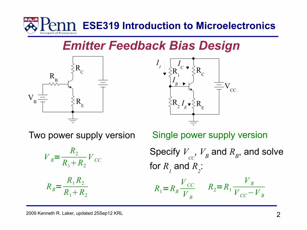
BJT Small Signal Models
Conceptually, the signal we wish to amplify is connected in series with the bias source and is of small amplitude.
We will linearize the signal analysisto simplify our mathematics – to avoid having to deal with thenonlinear exponential collector current
iC− I S evBE
V T
VCC
VB
RE
RCR
B

ESE319 Introduction to Microelectronics
72009 Kenneth R. Laker, updated 25Sep12 KRL
BJT Small Signal Models

ESE319 Introduction to Microelectronics
82009 Kenneth R. Laker, updated 25Sep12 KRL
Linearization Process
iC= I Cic= I S evBE
V T = I S eV BEvbe
V T = I S eV BE
V T evbe
V T
Split the total base-emitter voltage and total collector cur-rent into bias and signal components:
iC= I C evbe
V T
Identify and substitute the bias current into the model:
Expand the exponential in a Taylor series:
f x =∑n=0
∞
f n 0 xn
n!
I C
ESE319 Introduction to Microelectronics
92009 Kenneth R. Laker, updated 25Sep12 KRL
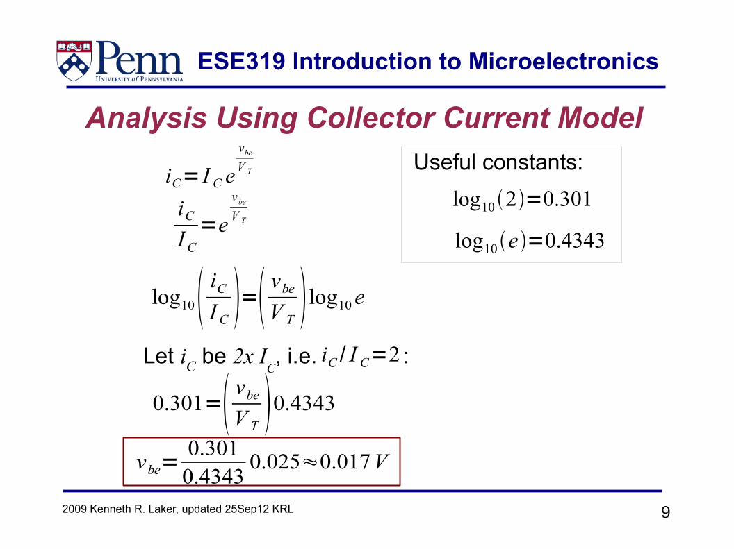
Analysis Using Collector Current Model
iC= I C evbe
V T
iC
I C=e
vbe
V T
log10 iC
I C = vbe
V T log10 e
log102=0.301
Useful constants:
log10e=0.4343
Let iC be 2x IC, i.e. :
0.301= vbe
V T 0.4343
vbe=0.301
0.43430.025≈0.017 V
iC / I C=2

ESE319 Introduction to Microelectronics
102009 Kenneth R. Laker, updated 25Sep12 KRL
Linearization Using Taylor Series
For the exponential func-tion:
f x =ex=∑n=0
∞ xn
n!
evbe
V T=∑n=0
∞ 1n ! vbe
V T n
or:
evbe
V T=1vbe
V T
12 vbe
V T 2
16 vbe
V T 3
≈1vbe
V T
Expand in a Taylor series: f x =∑n=0
∞
f n 0 xn
n!
when 12
vbe
V T2
≪1
ESE319 Introduction to Microelectronics
112009 Kenneth R. Laker, updated 25Sep12 KRL
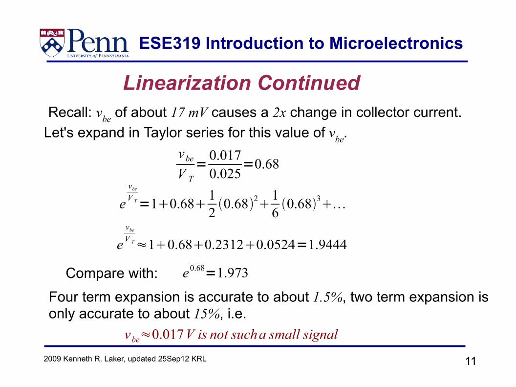
Linearization Continued Recall: vbe of about 17 mV causes a 2x change in collector current. Let's expand in Taylor series for this value of vbe.
vbe
V T= 0.017
0.025=0.68
evbe
V T=10.68 12 0.6821
6 0.683
evbe
V T≈10.680.23120.0524=1.9444
Compare with: e0.68=1.973
Four term expansion is accurate to about 1.5%, two term expansion is only accurate to about 15%, i.e.
vbe≈0.017V is not sucha small signal

ESE319 Introduction to Microelectronics
122009 Kenneth R. Laker, updated 25Sep12 KRL
Small Signal Model
And using the first two terms of the Taylor series expansion:iC= I Cic= I C e
vbe
V T
Using the grouping into bias and signal voltages/currents:
iC≈ I C 1 1V T
vbe= I CI C
V Tvbe=I Cic
We define transconductance and incremental (or ac) current as:
ic=gm vbegm=d iC
d vBEiC= I C
=I C
V T
bias current
ESE319 Introduction to Microelectronics
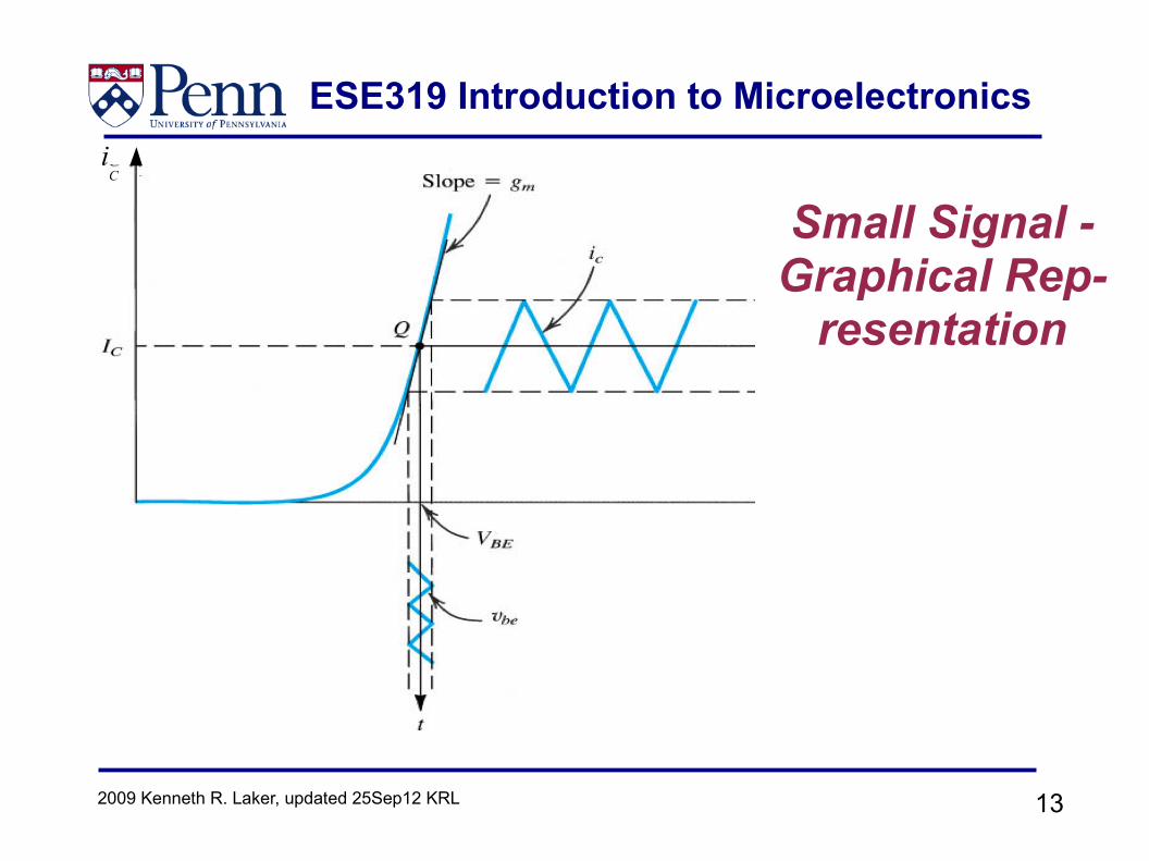
132009 Kenneth R. Laker, updated 25Sep12 KRL
Small Signal - Graphical Rep-
resentation
iC

ESE319 Introduction to Microelectronics
142009 Kenneth R. Laker, updated 25Sep12 KRL
Incremental (small-signal) BJT ModeliB= I Bib=
1
iC=1 I Cic
iB=1
iC=1
I C1 I C
V T vbe
Define the incremental base current and base resistance:
ib=1 ic=
1 I C
V T vbe=1r
vbe
r=V T
I C=
gmbias current
where I C=V T g m
I B ib

ESE319 Introduction to Microelectronics
152009 Kenneth R. Laker, updated 25Sep12 KRL
Equivalent ModelsEquations (3):
ic=gm vbe
ie=ibic
ib=ic
ib=
vbe
r
Equations (1):ic=gm vbe
ie=ibic
Equations (2):
ic= ib
ib=ie
1ie=1 ib=1
vbe
r=
vbe
re
Choose the model that simplifies the circuit analysis.
re=r
1=
1
V T
I Cic=gm r ib=
I C
V T
V T
I Cib= ib

ESE319 Introduction to Microelectronics
162009 Kenneth R. Laker, updated 25Sep12 KRL
Equivalent CircuitsEquations (3):
b
e
cic
g m vbe
ie=ibic
ib=ic
Equations (2):b
e
c
re
ib
ic= i bvce
r0
ib=ie
1
ie=vbe
re
Equations (1):
ib=vbe
r
ic=gm vbevce
r0
ie=ibic
rπ
b c
e
r r0
gm=I C
V Tr0=
V A
I C
r=V T
I B=
V T
I C=
g m
r0
re=V T
I E=
gm
=r
1
g m vbe r0
ic=gm vbevce
r0
icib
ie
ib ic
ie
ib ic
ie
ESE319 Introduction to Microelectronics
172009 Kenneth R. Laker, updated 25Sep12 KRL
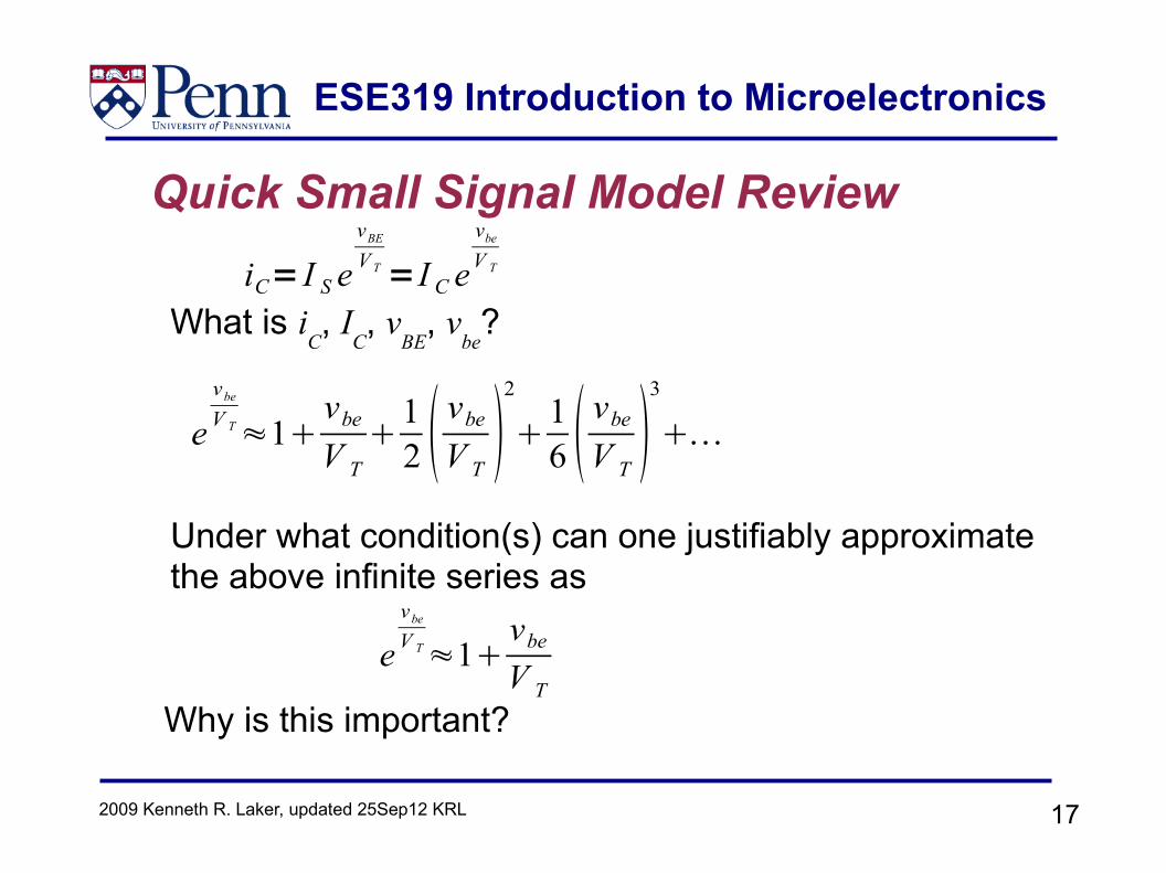
Quick Small Signal Model Review
What is iC, I
C, v
BE, v
be?
Under what condition(s) can one justifiably approximate the above infinite series as
iC= I S evBE
V T =I C evbe
V T
evbe
V T≈1vbe
V T
12 vbe
V T 2
16 vbe
V T 3
evbe
V T≈1vbe
V T
Why is this important?
ESE319 Introduction to Microelectronics
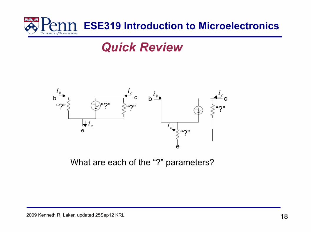
182009 Kenneth R. Laker, updated 25Sep12 KRL
Quick Review
“?” “?” “?”
“?”
“?”
What are each of the “?” parameters?

ESE319 Introduction to Microelectronics
192009 Kenneth R. Laker, updated 25Sep12 KRL
Quick Review
gm=I C
V T
r0=V A
I C
r=V T
I B=
V T
I C=
g m
re=V T
I E=
gm
=r
1

ESE319 Introduction to Microelectronics
202009 Kenneth R. Laker, updated 25Sep12 KRL
DC & AC Circuit Decomposition
RE
RCR
b
VCC
VB
RE
RCR
b
VCC
VB
RE
RCR
b
DC AC
DOES Rb = R
B = R
1\\R
2 ? ASSUMPTION: ?

ESE319 Introduction to Microelectronics
212009 Kenneth R. Laker, updated 25Sep12 KRL
DC & AC Circuit Decomposition
RE
RCR
b
VCC
VB
RE
RCR
b
VCC
VB
RE
RCR
b
DC AC
NO Rb ≠ R
B = R
1\\R
2
ASSUMPTION: signal v
s is pure AC!
ac source vs has
series input resistance
ESE319 Introduction to Microelectronics
222009 Kenneth R. Laker, updated 25Sep12 KRL
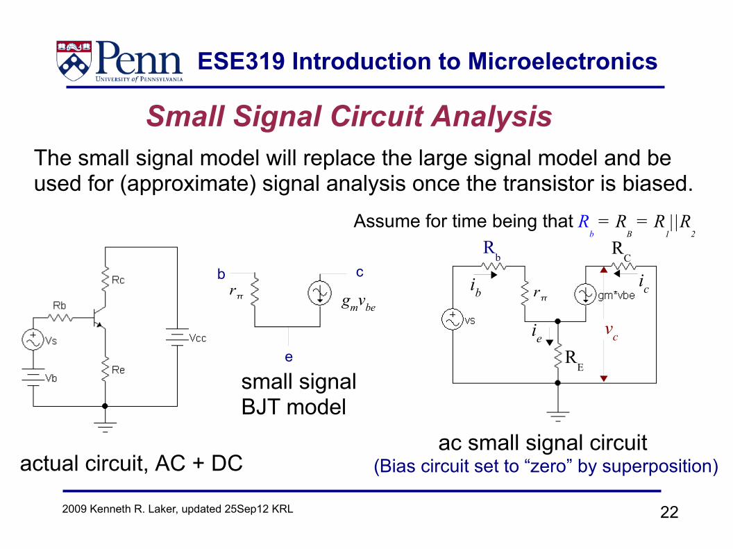
Small Signal Circuit AnalysisThe small signal model will replace the large signal model and be used for (approximate) signal analysis once the transistor is biased.
small signal BJT model
ac small signal circuit (Bias circuit set to “zero” by superposition)
gmvberπ
b c
e
r rib
ie
ic
vc
RC
RE
Rb
actual circuit, AC + DC
Assume for time being that Rb = R
B = R
1||R
2

ESE319 Introduction to Microelectronics
232009 Kenneth R. Laker, updated 25Sep12 KRL
Biased Circuit Small Signal Analysis
r=V T
I C=100 0.025
0.001=2.5k
vs=ibRbrie RE
vs=ibRbrib 1RE
ib=vs
Rbr1RE
vbe=ib r=r
Rbr1REvs
rib
ie
gm=I C
V T=
0.001 A0.025V
=0.04 S=40 mSNote: S = siemen
Let: =100 and I C=1mA
ic
vc
20 k Ohm
e
cb
RC
RE
Rb

ESE319 Introduction to Microelectronics
242009 Kenneth R. Laker, updated 25Sep12 KRL
Small Signal Analysis - Continued
vbe=ib r=r
Rbr1REv s
ic=gm v be=gm r
Rbr1REv s
gm r=I C
V T
V T
I C=
vc=−RC ic=−RC
Rbr1REv s
1RE≫Rbr⇒ vc≈−RC
1REv s
Av=vc
vs≈−
RC
RE
=100
rib
ie
vc
ic
20 k OhmR
C
RE
Rb

ESE319 Introduction to Microelectronics
252009 Kenneth R. Laker, updated 25Sep12 KRL
Multisim Model of “Bias Design”
Av=vc
vs≈−
RC
RE=−1
1. RE needs to be large to achieve good op. pt. Stability!
2. Consequence: |Av| is low.
20 k Ohm
RC
RE
Rb
VCC
VB
vs
vc

ESE319 Introduction to Microelectronics
262009 Kenneth R. Laker, updated 25Sep12 KRL
Multisim Input-output Plot
Av=vc
vs≈−
RC
RE=−1

ESE319 Introduction to Microelectronics
272009 Kenneth R. Laker, updated 25Sep12 KRL
Combining AC and DC Sources
vsv
s
vOR
S
RS
R1
R2
RC
RE
RC
RE
RB
VB
vO V
CCVCC
<=>
AC Source with low outputimpedance upsets bias.
Thevenin equivalent at base.

ESE319 Introduction to Microelectronics
282009 Kenneth R. Laker, updated 25Sep12 KRL
Combining AC and DC Sources Cont.
ISSUES:1. Signal source v
s shorts out V
B.
2. DC bias on vs interferes with op point design.
vs

ESE319 Introduction to Microelectronics
292009 Kenneth R. Laker, updated 25Sep12 KRL
“Blocking Capacitor” Remedy
vs
R1
R2
RC
RE
vO
VCC
RS
What is the purpose of “blocking capacitor” Cin?
How does one determine the value of Cin?

ESE319 Introduction to Microelectronics
302009 Kenneth R. Laker, updated 25Sep12 KRL
ConclusionsConservative voltage bias for best operating point stability and signal swing works, but returns unity voltage gain.
How does one obtain operating point stability, and simultaneously achieve a respectable voltage gain?

ESE319 Introduction to Microelectronics
312009 Kenneth R. Laker, updated 25Sep12 KRL
Conclusion Cont.How does one obtain operating point stability, and simultaneously achieve a respectable voltage gain?
Cbyp
“Bypass Capacitor”
“Blocking Capacitor”
vs


![Chapter 5 BJT Biasing Circuits Engineering/833... · 2017. 12. 8. · BJT Biasing Circuits 5.1 The DC Operation Point [5] DC Bias: Bias establishes the dc operating point for proper](https://img.dokumen.tips/doc/110x75/6109b3612d57d967952ea81a/chapter-5-bjt-biasing-circuits-engineering833-2017-12-8-bjt-biasing-circuits.jpg)