Embed Size (px)
Citation preview

NASA Technical Paper 2875
I
i
1989
National Aeronautics and Space Administration Office of Management Scientific and Technical Information Division
Universal Test Fixture for Monolithic mm-Wave Integrated Circuits Calibrated With an Augmented TRD Algorithm
Robert R. Romanofsky and Kurt A. Shalkhauser Lewis Research Center Cleveland, Ohio
https://ntrs.nasa.gov/search.jsp?R=19890008396 2018-05-27T21:00:09+00:00Z

Summary The design and evaluation of a novel fixturing technique for
characterizing millimeter-wave solid-state devices is presented. The technique utilizes a cosine-tapered ridge guide fixture and a one-tier de-embedding procedure to produce accurate and repeatable device-level data. Advanced features of this tech- nique include nondestructive testing, full waveguide bandwidth operation, universality of application, and rapid, yet repeat- able, chip-level characterization. In addition, only one set of calibration standards is required regardless of the device geometry.
Introduction The accurate characterization of solid-state devices at and
above K-band is hindered by limited metrological techniques due to increased parasitics, diminutive physical dimensions, and inconvenient interface methods (ref. 1). The quality of device characterization will inevitably affect the integrity of the intended application. Since many system applications can tolerate only marginal variations in device performance, much effort is spent in accurately quantifying radiofrequency (RF) parameters. Small-signal S-parameter techniques that use automatic vector network analyses are fundamental to this device evaluation.
Typically, microwave and millimeter-wave monolithic integrated circuits (MMIC’s), whether packaged or in die form, must be mounted in a fixture which provides a means to connect the chip to the automatic network analyzer (ANA) via coaxial cables or rectangular waveguide. The fixture introduces substantial insertion and return loss effects, both in magnitude and phase, often masking the true device charac- teristics. Calibration is normally done at the ANA transmission line-to-fixture interface by using known standards. Consequently, the measurement (reference) plane is removed from the physical device terminals by the fixture geometry. This discrepancy can be compensated for with a procedure known as de-embedding. The technique requires applying chip- level microstrip standards to mathematically shift the reference plane to the device area. A detailed discussion of the calibration and de-embedding procedures is given in the section Fixture Calibration.
Drawbacks of existing fixtures include the inability to obtain repeatable data, the difficulty in securing a device in the
fixture, the complexity of calibrating the fixture, and the limitations on bandwidth imposed by the waveguide-to- microstrip transition. In addition, most techniques are destructive to the device and are labor intensive. This report describes the evolution of a new test fixture with several innovative features that is operable over the K, band (26.5 to 40.0 GHz). A photograph of the fixture is shown in figure 1.
A cosine-tapered ridge transition matches the high waveguide impedance to the 50-0 microstrip. The taper length and profile have been analytically determined to provide maximum bandwidth and minimum insertion loss. Integrated circuits and devices are mounted on a customized carrier which is inserted between the bottom of the ridge and the base of the waveguide. The electric field is concentrated by the ridge and launched onto the carrier microstrip via direct pressure contact. Isolation between the device under test and the fixture, as well as biadcontrol circuitry, is also provided by the carrier. Control voltages are applied to the carrier by a self-aligned bias module with integral spring-loaded contacts. The carrier assembly is designed for direct insertion into a given system, such as a phased array, and thus serves the dual role of test vehicle and package. De-embedding is accomplished with through-reflect-delay (TRD) microstrip standards and software. These calibration standards set the ancillary reference plane at the bisector of the chip carrier. Then, the complex propagation constant of the carrier microstrip line is determined from the standards, and the reference plane is subsequently shifted to the device boundaries. Figure 2 illustrates this concept.
Chip Carrier Design The most complex component of the test fixture is the chip
carrier. Since the fixture itself is mechanically rigid to improve data repeatability, the required versatility was built into the carrier. A 0.020-in. alumina substrate was chosen for its manufacturability , good dielectric properties, and relatively good thermal and mechanical characteristics. The substrate thickness was constrained to a narrow range by line-width restrictions. Whereas the lithography process imposed a minimum feature size on the coupled-line section, the possibility of generating surface waves imposed a maximum substrate thickness. A 0.020-in. substrate was a suitable compromise for K, band. Features of the carrier include coupled-line direct-current (dc) blocks, input (gate) and output
1

.* mrc -
I TRANYII SS ION EDIA
.o CONDUCTIVE EPOXY FILM-
M I C TEST TRANYIISSION EDIA FIXTURE 7
Figure 1 .-Partially disassembled view of cosine-tapered ridge guide fixture along with through-rej7ecr-dehy (TRD) calibration standards. Monolithic 30-GHz gain control amplifier is mounted on carrier.
I
I L
(drain) bias filters, and 10 bias pads. A key feature of the design is a generic footprint; that is, except for a central area on the carrier, the metalization pattern is common for all chip and device types. Figure 3 highlights the carrier topology and demonstrates the assembly.
The dc blocks are required since the carrier microstrip lines are in contact with the fixture body, which is at ground potential. The obtainable bandwidth of the dc blocks is a strong function of the gap between the coupled lines. A 0.002-in. gap and a 0.032-in.-long coupled section with 0.0029-in.-wide fingers were found to be optimum (refs. 2 and 3). The dc block design was modeled with commercially available software which predicted an insertion loss of less than 0.25 dB over
,
CARRIER-
KOVAR SUBCARRIER -
(b) (a) Ihrough-short-delay (TSD) calibration standards.
(b) Chip carrier assembly.
Figure 3 .-Detailed schematic of calibration standards.
most of the band. The chip was mounted in a laser-machined well in the center of the carrier and supported by a gold-plated kovar subcarrier. A mesa was machined on the kovar subcarrier such that the surfaces of the chip and alumina carrier were flush. The mesa was extended beyond the width of the chip to accommodate chip capacitors, if necessary, and to facilitate grounding requirements. The carrier was bonded to the kovar with a special indium alloy preform by heating to 210 "C. Subsequent to this procedure, the die was attached with silver-impregnated epoxy which was cured at 125 "C. The carrier can accommodate chips up to 0.250 in. long.
Bias could be fed directly to the chip input and output microstrip lines, if required, through two bias filters. The filters consisted of a midband quarter-wavelength high impedance line cascaded with a quarter-wavelength, open- circuit, low impedance line. The input impedance of this combination was extremely high over a significant bandwidth and served to isolate the RF from the bias supply. Actual dc contact was made at the junction of the two quarter-wavelength lines so as not to perturb the impedance.
I 2
ORIGINAL PAGE IS OF POOR QUALITY
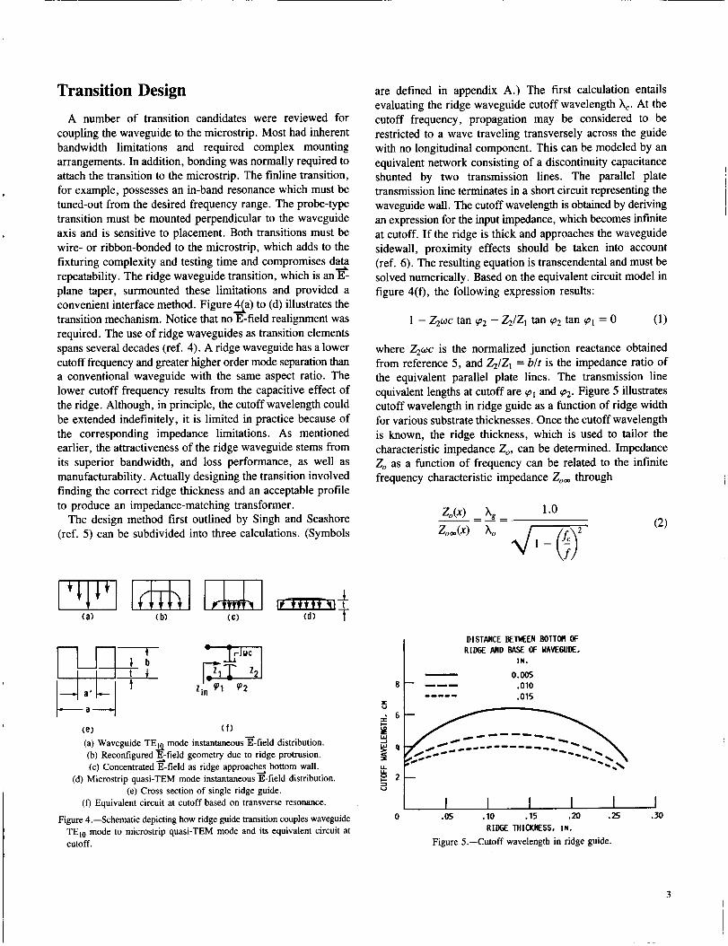
Transition Design A number of transition candidates were reviewed for
coupling the waveguide to the microstrip. Most had inherent bandwidth limitations and required complex mounting arrangements. In addition, bonding was normally required to attach the transition to the microstrip. The finline transition, for example, possesses an in-band resonance which must be tuned-out from the desired frequency range. The probe-type transition must be mounted perpendicular to the waveguide axis and is sensitive to placement. Both transitions must be wire- or ribbon-bonded to the microstrip, which adds to the fixturing complexity and testing time and compromises data repeatability. The ridge waveguide transition, which is an* plane taper, surmounted these limitations and provided a convenient interface method. Figure %a) to (d) illustrates the transition mechanism. Notice that no E-field realignment was required. The use of ridge waveguides as transition elements spans several decades (ref. 4). A ridge waveguide has a lower cutoff frequency and greater higher order mode separation than a conventional waveguide with the same aspect ratio. The lower cutoff frequency results from the capacitive effect of the ridge. Although, in principle, the cutoff wavelength could be extended indefinitely, it is limited in practice because of the corresponding impedance limitations. As mentioned earlier, the attractiveness of the ridge waveguide stems from its superior bandwidth, and loss performance, as well as manufacturability . Actually designing the transition involved finding the correct ridge thickness and an acceptable profile to produce an impedance-matching transformer.
The design method first outlined by Singh and Seashore (ref. 5) can be subdivided into three calculations. (Symbols
are defined in appendix A.) The first calculation entails evaluating the ridge waveguide cutoff wavelength A,. At the cutoff frequency, propagation may be considered to be restricted to a wave traveling transversely across the guide with no longitudinal component. This can be modeled by an equivalent network consisting of a discontinuity capacitance shunted by two transmission lines. The parallel plate transmission line terminates in a short circuit representing the waveguide wall. The cutoff wavelength is obtained by deriving an expression for the input impedance, which becomes infinite at cutoff. If the ridge is thick and approaches the waveguide sidewall, proximity effects should be taken into account (ref. 6). The resulting equation is transcendental and must be solved numerically. Based on the equivalent circuit model in figure 4(f), the following expression results:
1 - &oc tan cp2 - &/Z1 tan cp2 tan c p 1 = 0 (1)
where &wc is the normalized junction reactance obtained from reference 5, and &/Z1 = b/t is the impedance ratio of the equivalent parallel plate lines. The transmission line equivalent lengths at cutoff are cpl and q2. Figure 5 illustrates cutoff wavelength in ridge guide as a function of ridge width for various substrate thicknesses. Once the cutoff wavelength is known, the ridge thickness, which is used to tailor the characteristic impedance Z,, can be determined. Impedance Z, as a function of frequency can be related to the infinite frequency characteristic impedance Z,, through
= I - 8
DISTANCE BETMEN BOTTON OF RIDGE AND BASE OF WAVEGUDE.
IN.
7 0.005 .010 .015 _----
------ __-- ------_ Y
(a) Waveguide TE3 mode instantaneous z-field distribution. (b) Reconfigured %-field geometry due to ridge protrusion. (c) Concentrated E-field as ridge approach2 bottom wall.
(d) Microstrip quasi-TEM mode instantaneous E-field distribution. (e) Cross section of single ridge guide. " I
(0 Equivalent circuit at cutoff based on transverse resonance.
Figure 4. -Schematic depicting how ridge guide transition couples waveguide TE., mode to microstrio auasi-TEM mode and its eauivalent circuit at
I I I I I I I 0 .05 .10 .15 -20 .25 .30
RIDGE THICKNESS. IN. 1" ~
~~
cutoff. L .
Figure 5.-Cutoff wavelength in ridge guide.
3
where A, is the guide wavelength and A, is the free space wavelength. The impedance Z,, for the TEIo mode is given by Cohn (ref. 4) as
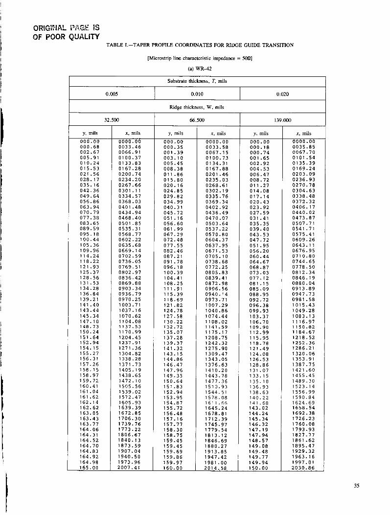
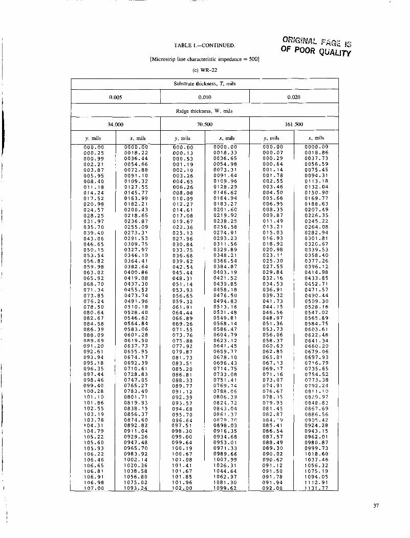
Test Fixture Radiofrequency Performance. Taper profile coordinates are included in table I for this 26.5- to 40.0-GHz case as well as other waveguide bands up to 110 GHz.
1207r2t Zom = (3)
t
Since the band of interest is significantly above the cutoff frequency, the radical in equation (2) approaches unity and Z, can be approximated by Z,, for the ridge thickness calculation. As for the cutoff wavelength, numerical techniques are required for the solution. The impedance Z, is a function of ridge height and, hence, a function of position along the taper. The final stage of the design process involves solving for the physical taper, the length of which should provide adequate bandwidth without introducing unnecessary loss. A sinusoidal variation of the form
z, + z, z, + z, n-x ZJx) = ~ - ~ cos -
2 2 P (4)
is assumed (ref. 8). With the possible exception of a Dolph- Tchebycheff profile, the sinusoidal taper outperforms other candidate tapers by minimizing the return loss in a given length. For example, a sinusodial transition performs as well as a linear transition but is only half as long. The length of the taper is P, and x is the position along the taper from its origin. The characteristic impedances of the open waveguide at x = 0 and the ridge guide at x = e, are Z, and Z,, respectively. Both impedances were calculated at the midband frequency. The taper provides a smooth transition from the full waveguide height to the substrate thickness and couples the dominant TElo waveguide mode to the quasi-TEM micro- strip mode. Substituting equation (3) into equation (2) yields an expression for the taper height I as a function of position:
( 5 ) \J /
t =
A computer program was written to calculate the ridge geometry, given the basic waveguide and substrate dimensional parameters. Based on the previous calculations, a taper length of 1.366 in. (3Xg at 26.5 GHz) and a ridge thickness of 0.0695 in. were chosen. A smooth chamfer was machined at the end of each transition to eliminate sharp edges and, hence, reduce radiation. Performance data are included in the section
Bias Module Design A single-piece bias module was developed to supply the
device being tested with the necessary bias and control power. The most important feature of this module is its ability to make solid, repeatable, nondestructive electrical connections to metalized pads on the alumina chip carrier. To do this, the bias module relies on the contacting properties of miniature spring-loaded plunger contacts. The contacts are mounted vertically in a single block of insulating material that serves as an alignment guide, contact support structure, and RF shield. This block is manufactured from a machinable material with dielectric properties similar to Lexan or Rexolite.
The bias module feeds power directly to the chip carrier through 10 spring-loaded contacts. Each contact consists of two parts-a spring-loaded plunger contact and a contact sleeve. Each plunger contact body has a slight deformation (bow) to retain it by friction in the contact sleeve. The obvious advantage of the two-piece design is that the pin contact can be easily replaced if damaged, or changed to another contact type if desired. A solder cup in the closed end of the contact sleeve provides a solderable connection to the pin assembly. Both the contact and contact sleeve are manufactured from nickel-silver alloy for high electrical conductivity. Each contact sleeve has a small rectangular collar on its open end. If the collar is carefully designed and machined, it can be used to seat the pin assembly and oppose the compression forces of the contact springs. This seating then maintains the vertical clearance of the pins over the chip carrier and ensures uniform contact pressure at all times.
To achieve the proper contact positioning, the bias module is equipped with precisely aligned holes parallel to the vertical axis of the contact block. Cylindrical posts inserted into the fixture base guide the bias module down vertically onto the chip carrier. The bias module is then secured to the test fixture with two thumbscrews to enable quick assembly and disassembly. Center-to-center contact spacing for this application was selected as 0.062 in. to provide firm mechanical support for the pin assemblies. The insulating material of the bias block provides electrical isolation.
If testing indicates the presence of severe electromagnetic interference, the bias module is designed to facilitate the insertion of an RF shielding structure. This shield may be nothing more than conductive foil lining the clearance cavity inside the bias module, or it may be a machined insert to the module. In either case, the cavity resonances must be considered to prevent misleading test results or unpredictable side effects.
In all, the bias module represents a novel, yet simple, way to apply the bias to the chip carrier. The design can be used
4
for a variety of carrier layouts and can be scaled to meet the needs of various frequency ranges.
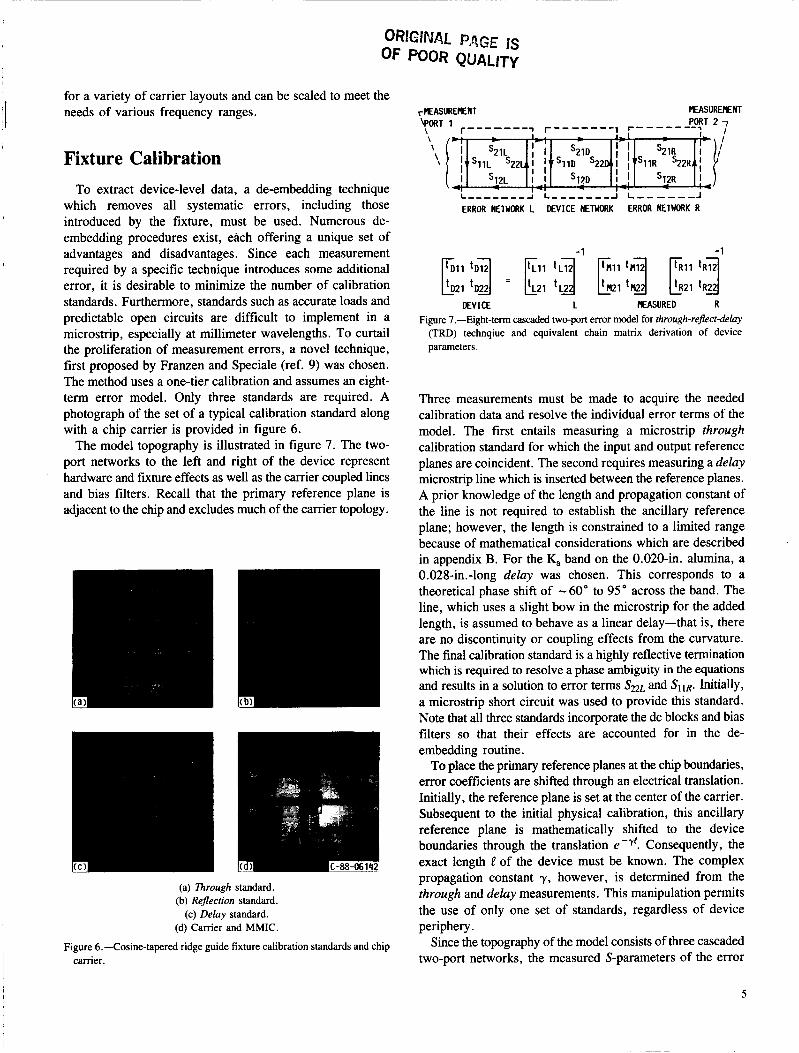
Fixture Calibration To extract device-level data, a de-embedding technique
which removes all systematic errors, including those introduced by the fixture, must be used. Numerous de- embedding procedures exist, each offering a unique set of advantages and disadvantages. Since each measurement required by a specific technique introduces some additional error, it is desirable to minimize the number of calibration standards. Furthermore, standards such as accurate loads and predictable open circuits are difficult to implement in a microstrip, especially at millimeter wavelengths. To curtail the proliferation of measurement errors, a novel technique, first proposed by Franzen and Speciale (ref. 9) was chosen. The method uses a one-tier calibration and assumes an eight- term error model. Only three standards are required. A photograph of the set of a typical calibration standard along with a chip carrier is provided in figure 6.
The model topography is illustrated in figure 7. The two- port networks to the left and right of the device represent hardware and fixture effects as well as the carrier coupled lines and bias filters. Recall that the primary reference plane is adjacent to the chip and excludes much of the carrier topology.
(a) lhrough standard. (b) ReJecrion standard.
(c) Delay standard. (d) Carrier and MMIC.
Figure 6.-Cosine-tapered ridge guide fixture calibration standards and chip carrier.
rllEASUREMENT MEASUREENT PORT 2 7 - r------- 1 I-------- ? I
' p T 1 -------
L _ _ _ _ _ _ _ i L _ _ _ _ _ _ _ J L _ _ - _ _ _ J ERROR NETWORK L DEVICE NETWORK ERROR NETWORK R
DEVICE L MEASURED R
Figure 7.-Eight-term cascaded two-port error model for through-rejlect-delay (TRD) technqiue and equivalent chain matrix derivation of device parameters.
Three measurements must be made to acquire the needed calibration data and resolve the individual error terms of the model. The first entails measuring a microstrip through calibration standard for which the input and output reference planes are coincident. The second requires measuring a deluy microstrip line which is inserted between the reference planes. A prior knowledge of the length and propagation constant of the line is not required to establish the ancillary reference plane; however, the length is constrained to a limited range because of mathematical considerations which are described in appendix B. For the K, band on the 0.020-in. alumina, a 0.028-in.-long deluy was chosen. This corresponds to a theoretical phase shift of -60" to 95" across the band. The line, which uses a slight bow in the microstrip for the added length, is assumed to behave as a linear delay-that is, there are no discontinuity or coupling effects from the curvature. The final calibration standard is a highly reflective termination which is required to resolve a phase ambiguity in the equations and results in a solution to error terms S22L and SI 1 ~ . Initially, a microstrip short circuit was used to provide this standard. Note that all three standards incorporate the dc blocks and bias filters so that their effects are accounted for in the de- embedding routine.
To place the primary reference planes at the chip boundaries, error coefficients are shifted through an electrical translation. Initially, the reference plane is set at the center of the carrier. Subsequent to the initial physical calibration, this ancillary reference plane is mathematically shifted to the device boundaries through the translation e Consequently, the exact length &' of the device must be known. The complex propagation constant y , however, is determined from the through and deluy measurements. This manipulation permits the use of only one set of standards, regardless of device periphery.
Since the topography of the model consists of three cascaded two-port networks, the measured S-parameters of the error
5
networks and inserted device can be converted to T-parameters for convenience. The T-matrix of the model is equal to the product of the individual 7'-matrices; therefore, the matrix of the de-embedded device can be extracted and reconverted to S-parameters (fig. 7). The mathematical derivation, which assumes that the microstrip characteristic impedance is 50 fl (independent of frequency), treats the left and right halves of the fixture independently-that is, no assumption is made regarding symmetry and reciprocity (ref. 10). Furthermore, the model neglects fringing capacitance from the microstrip line to ground at the input and output of the chip as well as any coupling admittance. Including these parasitic reactances would require additional standards, and this was contrary to the design philosophy of maximizing repeatability and accuracy by minimizing mechanical and electrical complexity. From the TRD measurements and the stated assumptions, all 16 terms (magnitude and phase) of the error networks can be determined.
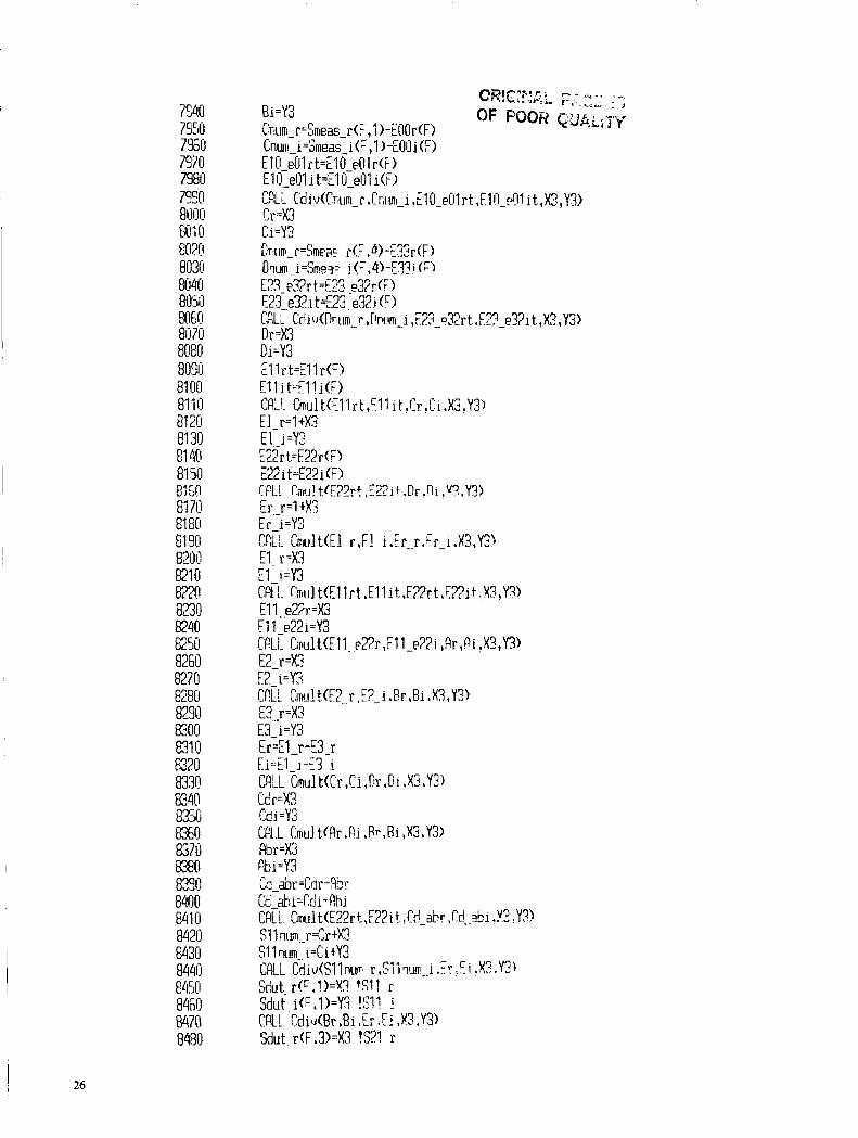
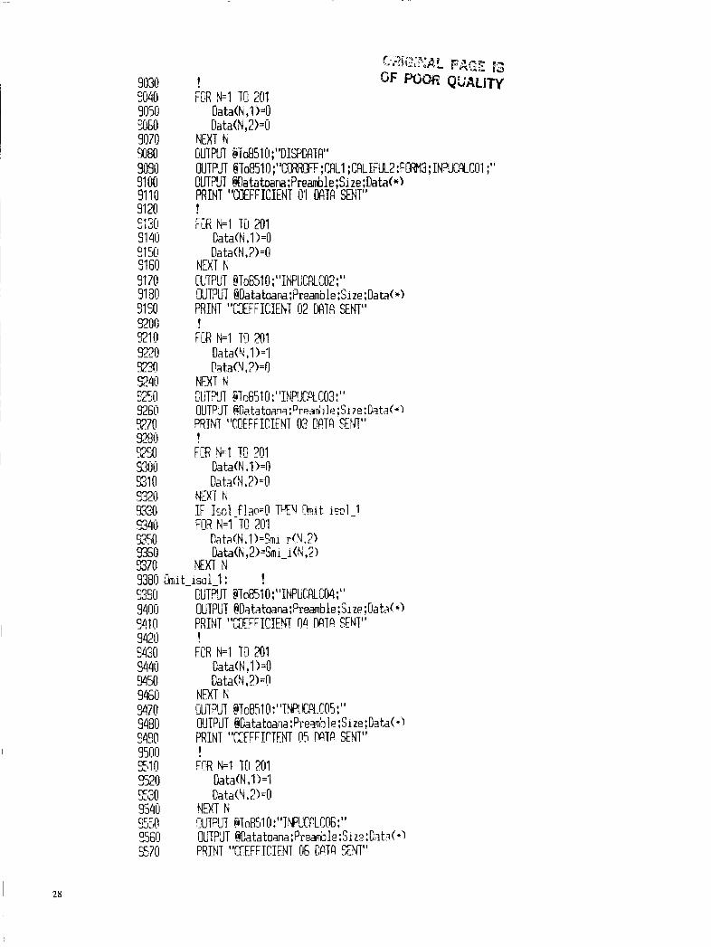
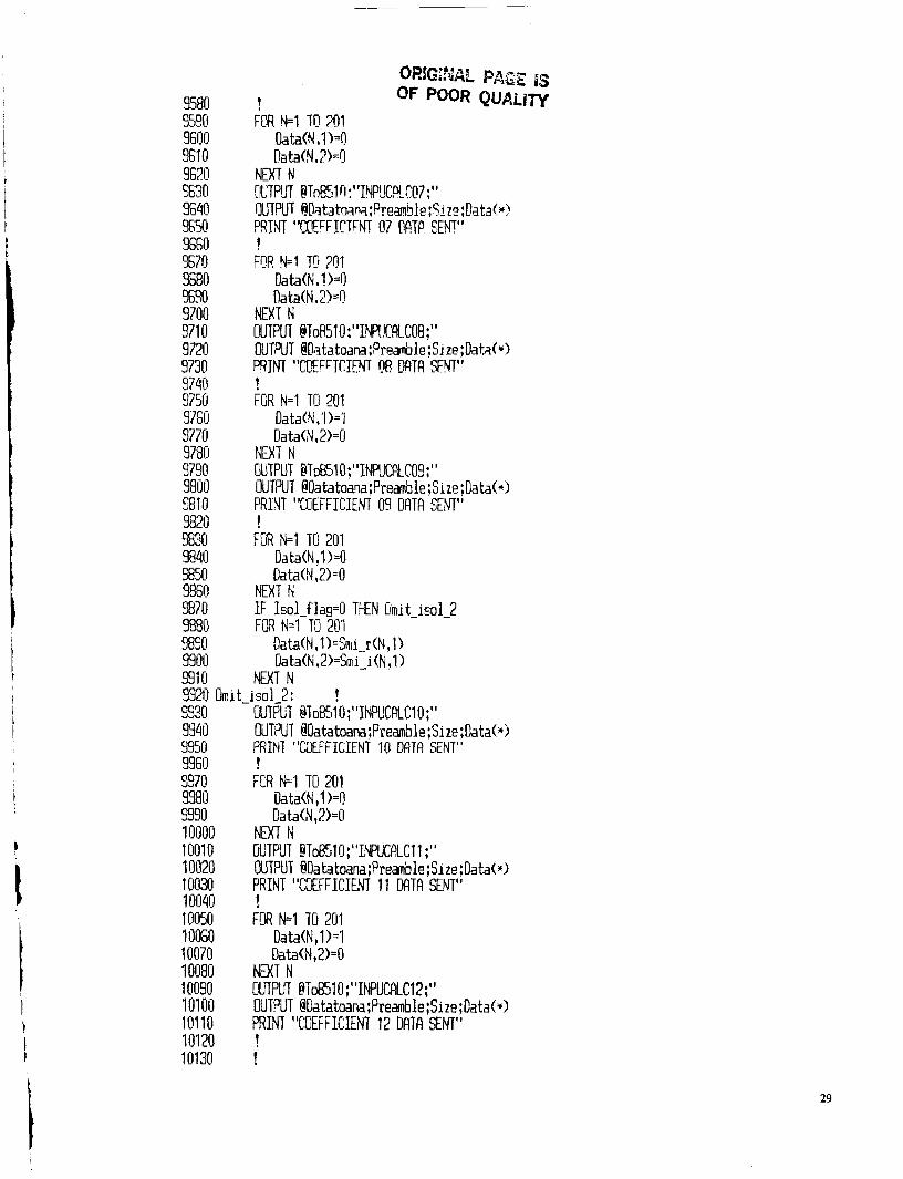
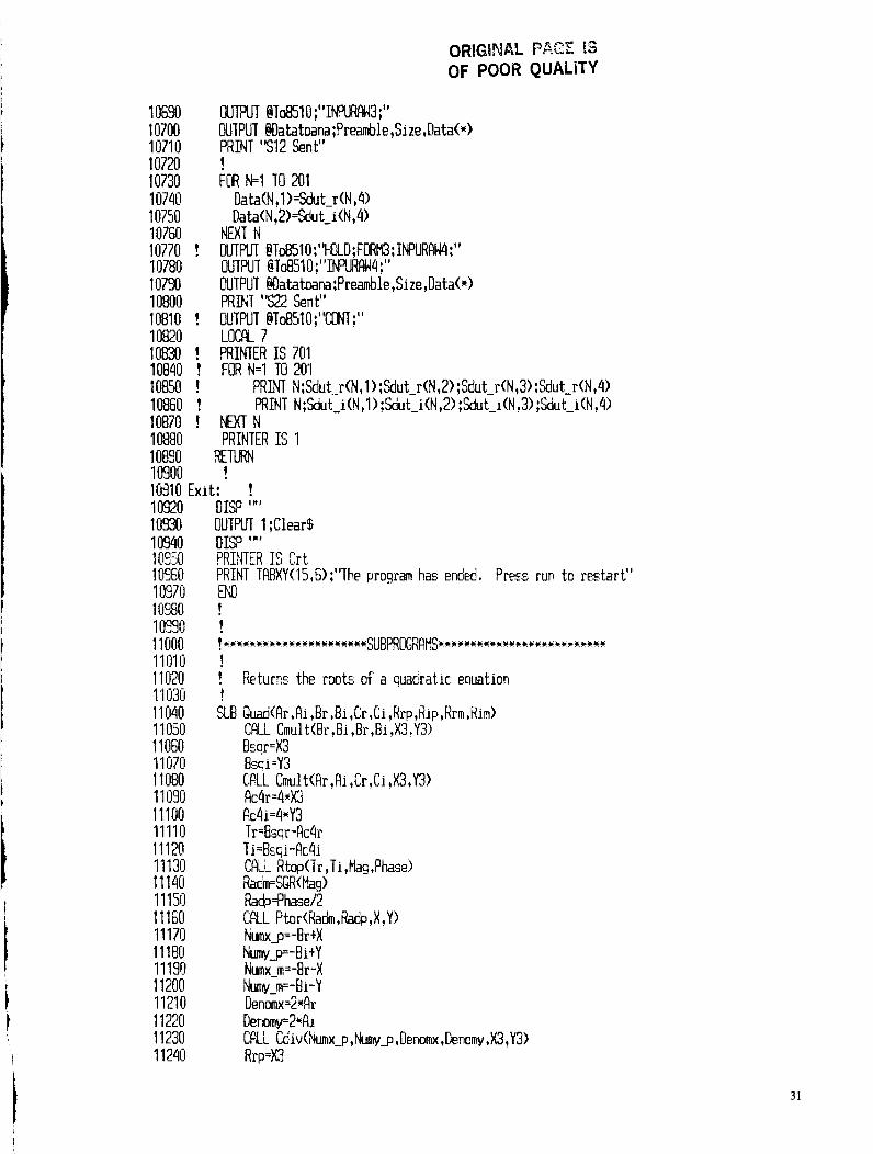
Software was created to carry out the enhanced TRD calibra- tion algorithm on a Hewlett-Packard 9836 desktop computer. The computer program, written in BASIC, performs all the instrument control functions, the data acquistion and transfer routines, and the TRD matrix calculations. This de-embedding code is shown in Appendix C.
The TRD program begins with the transfer of raw, uncorrected S-parameter data from the ANA. The data arrive in 10 sets: 4 sets describe the through standard (Sll, S 1 2 , SZ1, SZ2); 4 sets describe the delay standard (SI1, SI2, SZ1, SZ2); and 2 sets decribe the rejection standard (SI 1, SZ2). Each data set includes a complete 201-point frequency sweep and presents data in realhmaginary pairs. The data can be transferred directly from the active ANA trace memory or from storage locations on an internal tape drive. The transferred data are then held in computer memory and withdrawn by the TRD calculation subroutine as needed.
The second section of the TRD code performs the actual error-coefficient calculations. During this subroutine, each of the necessary calculations is performed at each step in the frequency range. The entire calculation procedure takes approximately 2 minutes. Once completed, the error-terms are stored in memory arrays. Each error term is made up of a real and an imaginary component, thereby correcting for both magnitude and phase aberrations of the test system. This set of eight error terms establishes the reference plane at the bisector of the through line.
To mathematically shift the reference plane to the edges of the device under test, the computer program must know the exact device length. The value is entered from the keyboard in mils (thousanths of an inch). This section of the program is isolated from the rest of the calculations so that different lengths can be entered without having to recalculate the eight basic error terms. This approach saves time and allows convenient testing of various sized chips. The original set of unshifted terms is retained for later use if needed. The shifted
error terms are placed in complex data arrays in a format compatible with the ANA protocol.
After the TRD error model has been generated, there are two possible methods to extract the device data from the full measurement. One choice is to extract the device data by using the set of eight error terms with the HP 9836 computer, and then to return the S-parameter data to the ANA for display. Since this is the most straightforward and accurate approach, it was adopted for this application. Unfortunately, the quasi- real-time display of the data is compromised. An alternative approach would be to translate the 8 TRD error terms to the HP 12-term error model. In this way, the ANA would resume control of the test system and the data trace would be updated virtually in real time. This approach is appealing because it would allow the engineer to actively tune or control the device under test while viewing the results. However, the adaptation to the 12-term model requires additional assumptions which may not be justified. The following error-term translations between the two models are (as given in ref. 11):
EDF = S ~ I L EDR = s22R
ESF = s 2 2 L ESR = IR
ERF = s 2 1 L s 1 2 L E S = O E M = O
ERR = S21RS12R
ELF = S 1 1 R ELR = S 2 2 L
s 2 1 R s 2 1 L = S12RS12L
Test Fixture Radiofrequency Performance The RF characteristics of the ridge waveguide test fixture
were measured with a Hewlett-Packard 8510 ANA. To extend the operating range of the analyzer to include the K, band, it was configured with a 26.5- to 40-GHz waveguide test set and the appropriate components to coherently up and down convert the test signals. This arrangement allowed error- corrected, two-port, S-parameter measurements to be made across the full 26.5- to 40.0-GHz frequency range while still maintaining the resolution and functionality of the standard HP 8510 ANA. Because the test set operates in WR-28 waveguide media, direct connection of the ridge waveguide test fixture to the measurement system is possible without transitions of any type.
The RF measurements were made on the ANA by using two different techniques. For evaluation of the test fixture, the ANA was calibrated with precision waveguide standards at the test set waveguide flange. This technique placed the calibra- tion reference planes at the input and output of the fixture so that the RF characteristics of the complete assembly could be measured. The waveguide standards included a flush short, a quarter-wavelength offser short, and a sliding termination.
Figure 8 displays the results of measurements made when the two cosine-tapered ridge sections were connected back- to-back on a special baseplate (no carrier or transmission line).
6

-lo r
30 32 34 36 38 40 FREPUENCY. GHZ
(a) SI, return loss. @) S,, insertion loss.
Figure 8.-Characteristics for two back-to-back cosine-tapered ridge guide transitions.
The results show approximately 0.7 f 0.1 dB of insertion loss (S2J with a corresponding return loss ( S , ,) of greater than 25 dB across the full waveguide band. These measurements verify the predicted performance of low loss and large operating bandwidth.
The next test was also performed with the reference planes placed at the flanges of the test fixture. A section of matched transmission line placed between the two ridge sections was used to test the quality of the compression connection to the microstrip. Figure 9 displays the results of this measurement; the transmission line and interconnect added from 0.25 to 1.25 dF3 to the loss total. Since the microstrip line itself imparts several tenths of a dB loss, each connection is apparently
o r -10 -
W a -40
-50'
- (a)
I I I I I I
0 L (b) I I I I I I
36 38 40 -4 '
26 28 30 32 34
(a) SI, return loss. @) S,, insertion loss.
FREWENCY. GHZ
Figure 9.-Characteristics of uncalibrated fixture with 0.5-in. section of microstrip line inserted between transitions.
responsible for a maximum of about 0.5 dB. The TRD algorithm can compensate for these effects.
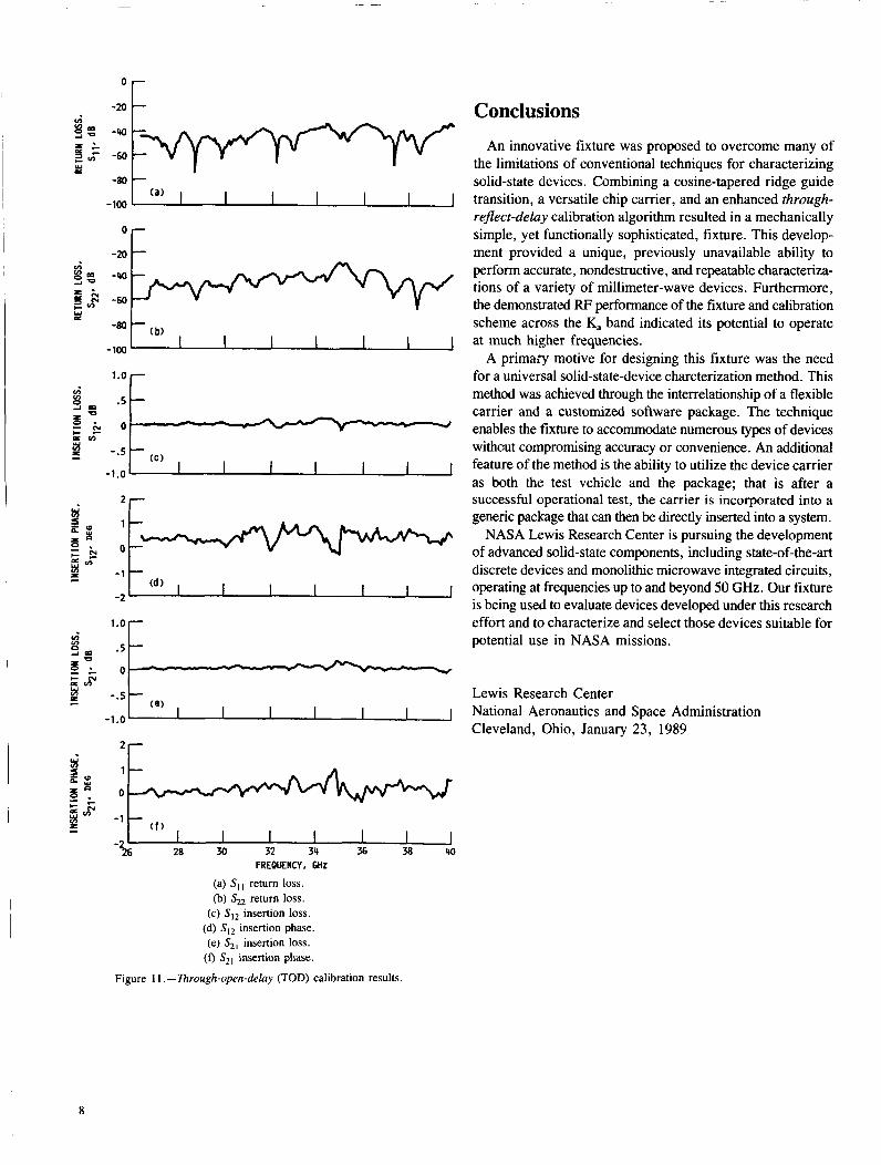
To test the accuracy of the TRD algorithm and associated hardware, the fixture was calibrated by using the through, short, and delay microstrip standards, and the error correction was verified by reinserting the through standard. This is equivalent to connecting the system without a test device. Ideally, this would result in 0-dB insertion loss, 0" phase shift, and infinite return loss. The actual test results are presented in figure 10. The insertion loss was measured at approximately 0.1 dB and the phase shift was 0.5". The return loss was measured at nearly 40 dB across the frequency range, thereby indicating a high quality calibration. During initial testing, SZ2 performance was marginal. Upon further investiation the electrical quality of the short circuit was found to be question- able. Therefore, an open circuit was substituted, and the fixture was recalibrated. These results are shown in figure 11. Insertion loss was better than 0.1 dB with a corresponding phase accuracy of 1 .O" . Return loss at both ports exceeded 40 dB across most of the band. The accuracy of these measure- ments approaches that of lower frequency calibrations and exceeds the accuracy and capabilities of similar systems currently available.
0 " - 1 - E (b)
-20 "c
-80 (C)
-1m2L 28 30 32 34 36 38 40 FREQUENCY. GHZ
(a) S,, insertion loss. (b) S,, insertion phase.
(c) SI, return loss.
Figure lO.-l%rough-short-delayuy (TSD) calibration results.
-m O L - Conclusions
-20 OL I
W a
(b) -80
-100
- I I I I I 1
1.0 r
I I I I I I
I Y I
I -1 !-- - td ) c
-2 I I I I I I
I 1-
0
( f ) -1
-2
- f I I I I I I
2a u) 32 34 36 38 40 26 I
FREQUENCY. GHZ
(a) SI, return loss.
(c) SI, insertion loss. (d) SI, insertion phase. (e) S2, insertion loss.
(f) S,, insertion phase.
I (b) S2, return loss.
An innovative fixture was proposed to overcome many of the limitations of conventional techniques for characterizing solid-state devices. Combining a cosine-tapered ridge guide transition, a versatile chip carrier, and an enhanced through- reflect-delay calibration algorithm resulted in a mechanically simple, yet functionally sophisticated, fixture. This develop- ment provided a unique, previously unavailable ability to perform accurate, nondestructive, and repeatable characteriza- tions of a variety of millimeter-wave devices. Furthermore, the demonstrated RF performance of the fixture and calibration scheme across the K, band indicated its potential to operate at much higher frequencies.
A primary motive for designing this fixture was the need for a universal solid-state-device charcterization method. This method was achieved through the interrelationship of a flexible carrier and a customized software package. The technique enables the fixture to accommodate numerous types of devices withcut compromising accuracy or convenience. An additional feature of the method is the ability to utilize the device carrier as both the test vehicle and the package; that is after a successful operational test, the carrier is incorporated into a generic package that can then be directly inserted into a system.
NASA Lewis Research Center is pursuing the development of advanced solid-state components, including state-of-the-art discrete devices and monolithic microwave integrated circuits, operating at frequencies up to and beyond 50 GHz. Our fixture is being used to evaluate devices developed under this research effort and to characterize and select those devices suitable for potential use in NASA missions.
Lewis Research Center National Aeronautics and Space Administration Cleveland, Ohio, January 23, 1989
Figure 11 .-ntrough-open-delay (TOD) calibration results.
8

Appendix A Symbols
a a’ b C
EDF EDR ELF ELR ERF ERR ESF
ESR
ETF E m EXF Em f,
Mij
P
h-plane width of the waveguide width of the ridge E-plane waveguide dimension junction capacitance directivity error term in forward direction directivity error term in reverse direction load match error term in forward direction load match error term in reverse direction reflection tracking error term in forward direction reflection tracking error term in reverse direction source match error term in forward direction source match error term in reverse direction transmission tracking error term in forward direction transmission tracking error term in reverse direction isolation error term in forward direction isolation error term in reverse direction cutoff frequency length of taper elements of matrix that is product of Tm,d and
--L
inverse of Tm.[
z,
elements of TL chain matrix representing measured delay standard chain matrix representing measured through standard chain matrix of error network to right of device elements of TR chain matrix of isolated through standard distance between ridge and base at substrate entries in left error chain matrix entries in right error chain matrix position along taper from origin characteristic impedance of ridge waveguide at x = L characteristic impedance of microstrip line infinite frequency characteristic impedance characteristic impedance of open waveguide at x = 0 characteristic impedance of parallel plate line of
characteristic impedance of parallel plate line of
impedance ratio of equivalent parallel plate lines normalized junction reactance
height t
height b
Y complex propagation constant Nij
SijR,SvL equivalent scattering parameter elements of resolved Ag guide wavelength
Smii measured scattering parameter element of short (PI electrical length corresponding to a ’ /2 Smtij measured scattering parameter element of through p2
Td chain matrix of isolated delay standard 0 radian frequency TL chain matrix of error network to left of device
elements of matrix that is product of inverse of Tm,[ and Tm,d A, ridge waveguide cutoff wavelength
error networks. free space wavelength
electrical length corresponding to (a - a ’)/2
9
l l r o Appendix B
gh-Reflect-Delay (TRD) Mathematil S
The basis for the derivation of the TRD algorithm is available in the cited references. An abbreviated summary of the mathematical technique is included herein to acquaint the reader with the procedure. A copy of the de-embedding routine, written in HP BASIC, is included for convenience. The TRD augmentation procedure, which relocates the reference plane to the device terminals, is also explained.
The measured scattering matrices are converted to chain (or transfer) matrices for mathematical convenience. By definition, the chain matrix for the through standard is
[TI = [; :] and the delay standard chain matrix, which assumes a frequency-independent 50-Q match, is
e-7' o [Tdl = [ 1 032) o e?'
The error networks to the left and right of the device are designated [ 7'' and [ TR], respectively. The equivalent chain matrix representation of the measured S-parameters of the through can be defined by
Similarly, the chain matrix representation from the delay measurement is
Multiplying [Trn,d] by [Trn,J yields equations of the form
where the Mu are entries in the resultant matrix [MI and tfij and tRu are entries in the left and right error matrices. Multiplying [TJ -' by [Trn,d] yields equations of the form
10
2
N12 ("> + (NZ2 -Nil) ("> - NZ1 = 0 (B7) tR12 lRI2
where the Nu are entries in the resultant matrix [N]. As mentioned in the section on fixture calibration, there are some constraints on the length of the delay. If the delay is very short, its chain matrix will approach the identity matrix and [T' and [TR] will be indeterminate. Also, if the delay is a half- wavelength multiple of the through and the associated propagation loss is small, a similar situation results. Therefore, the length must be chosen to avoid these extremes by some margin. This constraint limits the TRD technique to Octave bandwidth performance. However, the method is ideally suited to conventional waveguide operation for which the bandwidth ratio is typically 1.5. To utilize the full potential, one could design the entire measurement system in ridge guide, if a corresponding bandwidth could be realized with the chip carrier. Comparing the S-parameter equivalents of [T' and [Td shows
this information, the four unknowns can be resolved. Although the reflection calibration standard is necessary to
determine SZzL, it results in a quadratic, which implies a 180" phase ambiguity. Since the reflection should represent a low return loss with roughly a 180" phase shift, the uncertainty can be eliminated. Similarly, an open circuit should result in an in-phase (0") reflection. Also, the fixture uses the same reflection standard during the SI, and S2, measurement; therefore, no assumption is made regarding the equality of the measured reflection coefficients. The remaining equations result from straightforward algebraic manipulation and signal flow analysis and are listed for convenience as follows:
that IkLlllrD1I > ltL12/kz2l and that IkLllIh21> lkzl/fD2I. with

s12Rs12L = sMt12(l - s22Ls11R) (B14) the length of the chip and the complex propagation constant, the latter of which is determined from the through and delay measurements. Both the products of the transmission error coefficients and the reflection error coefficients are shifted through the translation e -?', where t is the device length. The BASIC program that solves for all eight complex error coefficients and interfaces with the network analyzer is included in appendix C.
The conventional TRD algorithm and the given standards would establish the reference plane at the bisector of the carrier. To shift the error coefficients to the chip terminals, the equivalent electrical length (including loss and dispersion) representing the chip must be known. This requires knowing

12
Appendix C Program to Solve for Complex Error Coefficients
This program implements the through-reflect-delay de- embedding technique using the Hewlett-Packard model 8510B network analyzer and the model 9836 computer/controller. This version of the software (B3) is designed for use with the
millimeter-wave test set for frequencies between 26.5 and 40.0 GHz.
Currently configured for open standard. See lines 6910,6920.
270 ! 220 ! E(l Ini tializatiorl: ! 3110 ClearB=Cm(l2 ) 310 LUT&T 1;ClrarB
Crt='l Prir!t~r=7(ll
CIPTICN B E 1 D;G ! Thru-f l aq4 Short-f lag% Del ay-f 1 ag=U Out-f lac=O Calc-f l ag4 Moae 1-f ias=l:i
P8INTEd I! Ck.1
t
PRIhT TREX10):" ?RIP;? ln'
PSIhT PRINT TFB(10) ;"You have just activated the Tt,iiU-Stii;'FiT-EiELFlY calibration I'
PRIgT TRB(1iN;"pro~r~. To operate the program, Dlesse folloili the I '
?RIM TPB(l0);"instructiorrs as tky w e a r on this screen," P m l T 111)
PAIhT "" PRIhT Tr?B(lU);"XITE: fin IiEE-488 cade nust cortr,ect this computer'' PRNT TAB(10);" to the 1" 8510, 1rr;tall the cable OF the connector" Prii!iT TFH10) ;'I labeled 'PP-IB' orl the rpar of the analyzer." P a ?
PRIhT TPEX10):"**
I '
PHII;T 1111
! !
EF t ab1 i E he: Inpu t/Gu tgu t aata tra.r;;fer pathr ,
I '
I'
1 1
I '
I I
I '
ORIGINAL PAGE IS OF PQOR QUALITY
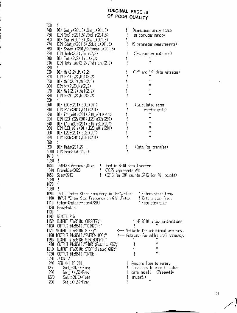
730 740 750 760 770 780 790 800 81 0 820 830 840 850 860 870 830 &%I 9uo 91 0 9x1
940 950 960 970 980 s50 1000 101 0 1020 I030 1040 1 EIS0 1 IlGO 1070 IO30 I 090 IlOii 1110 1120 1130 1140 1150 1160
9311
! Dimensions array cpace ! i n computer memory. I I1
! (S-parmeter meamemenid
! (T-parameter matrices1 ! !
I 1
I 1
! ! !
! ! ! ! ! ! ! !
! !
(Calculated error coeff icientd
I 1
I 1
I 1
I 1
I 1
I I
(Dat.a for transfer) I I
INTEGER Preamole,Size ! Used in 6510 data transfer Preamble=91)25 ! (9025 represent:; m Si ze=3215 ! (3215 for 201 poirits,6416 for 401 points) ! ! ! INPUT "inter Start ireuuercy in GHz",istart INPGT 'Enter Stop Frequency i n GHz",Fstop Fste~=(Fs tar t-Fs te.p)/200 Freq=Fs tar t ! REMTE 716 OUTPUT No851 0;"CGRROFF;" OUTPtiT @To8510;"PUIN201 :I1 !
! Enters start freq. ! inters stop f r q , ! Freq step size
! SP 8510 set-up instructions I 1
1170 !tiLITPUT BTo85lO;"FTEP;" 11 80 !OUTPUT @To851 0 ;"FIVER841 I100 ; ' I
1190 U U T W T @To8510;"SINC;CP~Nl ;I'
12011 OUTPdT @To35lO;"STAR";Fstart ;"GHZ: 1210 OUTPUT @To851 0;"STUP";Fstop;"GHZ;" 1220 OUTPUT @To3510 ;"ENTU;" 1230 LOCClL 7 1240 FOR N=l TO 201 1250 Smd-r(t ,5>=Freq 12G0 Smd-i (N,S)=Freq 1270 Smt-r(N,V=Frec 12EO Smt_i(N,S)=Freq
l l
Rctivate for additional accuracy. Flctivate for additional accuracy,
! ! ! !
I t
I1
I 1
I 1
! Rssigns freq to mernory ! lucations to ease i n later ! data recall, (Presently ! unuseb., ! I #
13

12% Sms-r(4,3 1 =,req ! 1 ~ ~ I ~ l Srn-i(?{, 3) =i r w ! 131 0 Suut-r(i .5)=?rer i 1220 $Cut-i(N,S)=Freq ! 1330 Fres=Freq+fstao ! 1240 NEXT N ! 1350 ! 1260 ! 1370 Menu: ! 123 [IISP 'I Erlt.er ieEired f u x t i o n cn Eaftwys nelcw" 1390 Oh K;Y 0 LRB~L "Ttl;IU" G13SllE Thru 1400 Clu KEY 1 3BE; "WIHT" G W B Short 1410 Oh EY 2 LABEL "DELRY" G B J E Ijelav 1420 C N KEY 3 ikEEL "KRS [JUT" GtiSiB Dut-meas 1430 OK KEY 4 LFlBEL 'I" GOT11 Menu 1440 CIN KEY 5 LRBEL "CHLCJLRTE" GOSUB Calculate 1450 uE.I KEY 6 LQB2 "SiND MljDCL" GOSiJE Sed 1460 EN KEY 7 LHBEL "SEM [IRTF," GCEi Sed-actual 1470 M KEY 6 LRBEL "" GOTO Menu 1480 CiY KEY 9 LRGEL "EXIT" GSTD Exi t 1490 GUT0 Menu 1Ei!U ! 1510 ! 1:20 STiiP 1530 ! 1540 ! I550 ? 1YdI ! 1570 !
15913 ! 1600 Thru: ! &acE S-mraieter data on the "TkRU" 1610 ! ca l ib ra t io i standard froin the HP 9510. 1620 ? (Data ir1 real. inacinary data Dair:.) 1 a 1 ! 1aIU [,IS? l ' g '
1650 P W T 3 IS Crt 1 660 CUTPET 1 ;Clears 1570 BEE? 1 EB0 1690 1700 PHLSE 1710 UUTPLT 1 ;Clear$
I*
I'
I I
, I 1
'I
?RINT THBXY(li1,6,:"Irl~ert the TkRU stancara i~ the FDRMlRLI direction'' DISC "?re;; CCNTIYJE tc Proceet'
1740 R Y i l T E 716 1750 ItUT?LiT ET0851 0;"C~RRUFF:" 17511 ! 1770 Sll-thru: ! &acs S11 "TbRLf' data from 8510 1780 IIUTPUT @To8510;"S'I 1 ;SING:" 1730 OliTi'IJ7 ETdSlO;"iCRH3;CUT~Wl:" 18il0 WTEFi @From851 U;Freamble,Size ,fuwaata(*) 1810 FOR N=l TU 201 1820 1830 1840 NEXT h
Sm t-r (N ,1 Hiewdata(N, 1 1 Smt-i (N ,1 )=Nedata(Ei, 2)
14
m?!GINAL 13 OF PmR QuaLlry
1 8% LiliTPUT PTo8SlO;"CONT;" 18611 ! : 870 ! 1880 S2l-thru: ! Reads 521 "TFRLI" data from 8YO 1891) OUTPJT fiTo8Y D ; W ;SING;" I900 OUTPUT @To8510 ;"FOKM3;C'UTPRPbil : I '
19'1 0 1920 FUR N=l TU 201 1930 Smt_r(N,3)=hewdata(h,ll IS40 Smt i (N, 3)=kwda taOi, 2) 1950 NEXT 1960 OUTPUT ET0851 O;"CGNT;" 19711 ! 1980 ! 1990 ! 2000 UISP ' ) ' I
2111 0 PdIkTEd I S Crt
ENTER @From851 I1 ;Preamble ,Size ,Newda t d 4 )
XI20 ClUTPllT 1 ;Clear% 2030 aw 2040 2050 2060 PAUSE 2070 OUTPUT 1 ;Clear$ 2080 DISP '111
2090 PRINT TPEXY(35,EJ :"PLEA% WIT" 21 00 ! 2110 ! 2120 Sl2-thru: ! 2eads S12 "THRU" data frcm 8510 2130 OilTPUT @To851 0;"S12;SING;" 21 40 OUTPUT ET08510 ;"FCiRH3;OUTPRRWl :" 21 50 ENTER @From85lll;Preamble ,Size ,Newdata(*) 21 60 FCR N=l TO 201 21 70 Sm t-r(ti ,Z)=fjewdata(N, 1 1 21 60 Smt_i(N,2>=kdata(N ,2) 21 30 NEXT h 2200 UUTPUT @To85 1 O;"CL";" 221 n ! 2220 !
PRINT TAEXY(l0,6):"Insert the THRU standard in the REVERSE dirertion" DISP "Pre;s CIBTINUE to proceed"
1
2230 S22-thru: ! Reads 522 "THRIJ" data from 8510 2240 OUTPUT @io851 0;"S22 ;SING;" 22% 2260 2270 2zall ;290 23130 231 0 2321) 2330 2340 2350 ZSU 2370 (7380 2390 2400
CIUUTPUT @To851 U;"FEfl!I3;L7UTPRAWl :I'
ENTER @From8510;Preamble ,Size ,herdata(*> FCIR N=l TU 201
NEXT ti- OlilPU @To851 0;"CON-l;" ! !
Smt_r(N,4)=Nwdata(N,I 1 4 t i (N ,4 )=Nedata(N, 2 )
PRINTER I S Crt! FUR N=l TO 211'1
NEXT N
Prints "THRU" data
PRINT Smt_r(N,1),Srnt_r(N,Z),Smt_r(N,3),Smt_r(N,4)
ik? "Pres CC;NTINUE to proceed." PRUZ OUTWT 1 ;Clear$
15
241 0 2420 2430 2440 2450 2460 2470 24Eo 2450
?RINT "Transfer o f 'ThRLJ' data completed" UdTPUT @To8SIU;"CUNT;" Thru-flay=l LOCk 7 ZT UR"I ! t
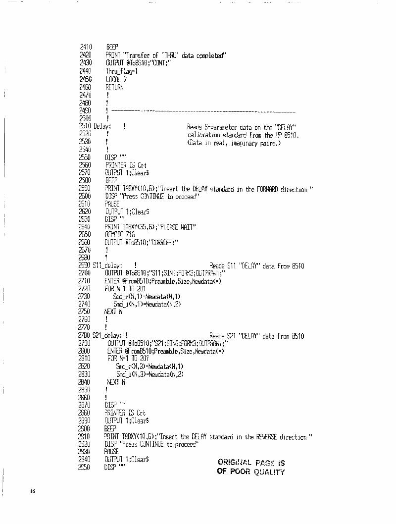
250II Zlil M a y : ! ?ea& S-mmeter oata on the "[IELFIY" 2520 ? calioration stanaard frofi the Hp 8510. z120 ! (Lata in real, imapinary pairs,) 2540 !
2790 mo 281 0 3 2 0 2831j 2840 2850 36ir 2'170 :%[I 2890 Et10 3 1 il 25.20 330 2940 E50
2550 DIS? 111 '
E7U I8I;TPIIT 1 :
2550 26111j 2510 ?RUSE 2S20 !XTJJT i ;ilearS ; a 0 LIS? 'I"
2540 PRINT TGBXY(3St6) ;"PLE&i #IT" 2550 REMSTE 716 2560 CUT?UT GTo8510;"CCRREFF :I'
2670 ! 2580 ! E20 31-delay: ! 3eao~ S1 1 "DEifiY" data from 8510 27011 UdTPUT ETo851Il;"S11 ;SI"IG:~II+~;;~~T~,&,~.~~ ;'I
271 0 27211 FOR h=l T i l 20'1 2730 Srrd-r(N,I>=fYewdata(N,l) 2740 Smd i(h,l>=fuewaata(h,2) 27Ed NEXT N- 27611 ! 2770 ! 2780 S21-delay: !
2560 P m m I 2yJ[j 8 7
?6hT TF,GXY(l0,6);"Iri~ert the UELRY Etarifard i n the FCiRWIl direction ' I
DIY "?res.; CIJ~TINIIE t o orocee?"
EIlTER BFrMn651 O;Prearrrble,Size ,hedata(*)
&ad._ S21 "LELRY" data from E510 UUTPdT $To85 1 O;"S21 :SING :idR% ;17UT%Fdu'l; ' I
ENTER homS51 O;Preable,Size ,hedata(*) FOR h=l TO 20'1
NTPUT 1 ;Clear$ 1'1'
I 16
OWEGIMAI PAG,: is OF PQOR QglALl7-Y
E60 PRINT TRRXY(35,6);"PLERSE MIT" 2470 ! 3 8 0 ! 3 5 0 S12_delay:! 3000 31 0 3020 FOR N=l TO 20'1 330 Srrd_r(N,2)=Newdata(N, 1 ) 3040 Smd-i(N ,2)=Newdata(N,2> 350 N E X T N 3060 ! 3 7 0 ! 3180 92-delay: ! Heaos 92 "UELAY" data from 8510 309U 31 00 3110 FOR N=l TO 20'1 31 20 Snd r(N,4)=Nedata(lu,l) 31 30 !hEi(N ,4>=Nedata(ti ,21 3140 NEXT N 31 50 ? 3 i 60 ! 3170 PRINTER IS Crt! Prints "UELRY' data 3180 FUR N=l TI1 20'1 31 31
&?ads S12 "[IELRY' data from 851s OUTPUT @To851 0 ;"SI 2 ;SING ;FUR3 ;dliTPRRbll;" ENTER @From851 0;Prearrble ,Size ,Newdata(*)
OUTPUT @To851 I1 ;'IS22 ;SING;FUWfI ;OUTPRPjr;l ;" ENTER From851 O;Prearrble ,Size,Newlata(*)
PRINT Smd-r(h, 1 ) ,Smd_r(h,2> ,Smd-r(N,3) ,Smd-r(N,4) 3200 NEXT N 3210 DISP "Press CUNTINLIE to proceed." 3220 PflUSE 330 UUTPUT 1 ;Clear$ 3240 BEEP 3250 3260 ULlTPUT @To%10 :"CIlNT:"
PRINT "Transfer of 'DELRY' data completeo"' _ _ _ ~
3270 Celay-f lag=l 3280 LOWL 7 3290 RETliRN 3300 !
! 31 0 3320 3330 ! 3340 Short: ! Reads S-parameter data on the "SK iT " 3350 ! calibration standard from the HP 8510, 3360 ! (Data i n real, imagriary pairs.) 33713 ! 3 6 0 UISP ""
3390 PRINTER IS Crt 34011 ULlTPUT 1 ;Clear% 3410 BEEP 3420 3430 3440 ?RUSE 3450 OUTPUT 1 ;Clears 3460 UISP "" 2470 PRINT TRBXY(35.6) :"PLERSE MIT"
)--------------------------------------------------------------
PRINT TFIBXY(20,6);"Insert the SWRT a t port 1 i p F l J " l direction'' OISP "Press CCNTINtlE to proceed"
3480 REMOTE 716 3490 DUTPUT @108510;"C~iRROF~;" 35011 ! 3510 511-short: ! Reads SI1 "SEEHT" data from 6510
OUTPUT @To851U;"S11 ;SING;FO&U;UUTWI ; I '
ENTER ff rod51 O;Premle,Size,Nta(*) FUH N=l 711 20'1
NEXT N- ! PRINTER IS Crt OtlTPUT 1 ;Clear$ EEP PRINT TRBXY(20,6):"Ir5~!rt the WRT a t Port 2 in 8EUERSE direction" DIP "Press MUTINLlE to proceed" P R E wUlll ;Clear$ RIhT TRBXY (35,6) ;"PLikSE WIT" !
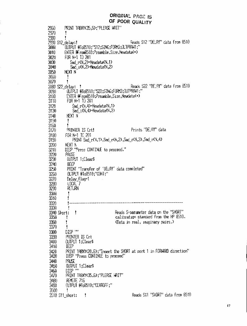
Sms_r(N,l )=Newdata(N,l) !h i(N,I)=Newdata(tu,2)
S90 S22-short: ! &ads S22 "SPORT" data from 8510 OUTPUT 810851 0 : "92 :SING :FWi :DUTPHWl : I ' 37013
371 0 3720 3730 3740 3750 3760 3770 3780 37911 mu 381 11 3820 3830 3840
3 6 0 3870 3 3 0 3890 3200
3aso
ENTER ff ro&1 d:Preamble ,Si ze .hiewdata(*) Full N=l TO 213'1
%~.-r(N,2)=Nedata(N,l) !ins-i(N , 2 ~ W a t a ( N ,2)
NEXT N ! !
PRINTER IS Crt! FUR h=l TE 20'1
Prints "S+fiRT" data
DISP "Press CONTINUE to proceed." PRilSE OUTPUT 1 ;Clear$ BEEP PRIhT "Transfer o f "N' Data mrpleteti" WTPUT @To851 0 ;"UINT ;" Shor t-f lag= 1 LOCH! 7 RETURN ! ! !
3940 Out-mas: ! Reads S-parmtpr data on the "[!UT" 3950 ! frm the tin 8510, 3560 ! (Cab i n real, imagirlary data pairs.)
! 3570 3530 3990 PAINTER Is Crt 4000 r!IPUT 1 ;Clear$ 4111 0 BEEP 4 2 0
1'11
%IN1 TRBXY(10,G);"Imrt Cb~ice Llrder Test i n FfiRWI direction I '
4030 4040 P F E 4050 OUTPUT 1 ;Ciear$ 40w DISP I " '
4070 PRINT TRBXY(35,6) ; " K E R S %IT"
DISP Tress MNTINUE to proceed'
18

4080 REMOTE 716 490 41 00 ? 41 10 ! 4120 Sll-meas: ! iieads S11 "UUT" data from 8510 41 30 OUTPUT @To8510;"S11 SING:" 41 40 41 50 41 60 41 70 Smeas-r(N ,I ~=Newdata(iJ,I) 41 80 %eas-i(N, 1 )=Newdata(N,2) 41 90 NEXT N a0 OUTPUT @To851 0;"CCM ;" 421 0 ? 4220 ! 423tl :21-ms: ! Reads S21 "Et!T" data from 8510 4240 WTPUT @To8510;'521 ;SING:" 4250 OUTPUT @To851O;"FD~3;WTPRRW1 :'I 4260 ENTER @From8510;Preamble,Size ,Newdata(*> 4270 FOR N=l TU 201 4280 Sm~~_r(N,3)=Newdata(E;,l 1 4290 Smeas-i(N, 3)=Newdata(N ,2) 4300 NEXT t.i 431 0 4320 ? 4330 ! 4340 UISP ''I1
4350 PRINTER I S Crt 4360 OUTPUT 1 ;Clear$ 4370 BEEP 4380 4390 4400 PRliSE 441 I1 4420 4430 4440 ! 4450 ! 4460 S12-meas: ! Reads 512 "[)UT" data from 8510 4470 UUTPUT @To851 0;"S12:SING;" 44811 44911 ENTER BFrom8510;Preamole ,Size .Newdata(*) 4500 FOR N=l TCI 201 451 0 Smeas-r(N,2)=Eieudata(N,l> 4520 Sweas_i(N,2)=luewdata(N,2> 4530 NEXT h 4540 WTWT @To8510;"C€iNT ;" 4550 ? 4560 ! 4570 S22-meas: ! Reads S22 "[KIT" data from 8510 4580 OUTPUT @To851 0;"522;SING;" 4590 UUTPM @To8510;"FORM3;OUT~l;" 4600 ENTER @From851U;Preamble ,Size .Newdata(*> 461 0 F"' N=l TO 201 4620
OUTPUT @To851 0 ;"(;GRRCFF ; "
OUTPUT @To851 0 : "FURM3; CUTPRFIWl ;'I ENTER @FromS510 ;Preamble ,Size . Newda ta( *> FOR N=l TO 201
UUPUT ET0851 0 ;' 'CDNT ;' '
PRINT THBXY(10,6);"Insert Device Umer Test in REWRSE direction ' I
DISP "Press CINTINUE to proceed"
UUTPUT 1 ;Clear$ DIP ' " 1
PRINT THEXY (35,6) ;"PLERSE HIT"
OUTPUT @To851 0 ;' 'FGRM3 ; CQJTPRRwl ; "
d~iw-r (N ,4)=Newdata(N, 1 )

t
[ E P "Press KINTINLE to proceed." pq ICC
WT?UT 1 ;Clear$ BE@
PRINT "TrarE,fer of '[JUT' data mvle ted ' OUTPUT @To8510;"C!XT:"
I bdL
ETURN ! !
!
4 3 0 4640 4650 46S0 4670 4Ea 4690 4700 471 0 4 7 3 4730 4740 4750 47511 4770 47s0 4790 4800 481 0 4820 11830 4840 4850 Calculate: ! ?erform a l l TSD mathematics, includirq 481;O ? matrix m d i i d a t i o n s and calculation 48711 ! of error coefficients,
4890 NITP9T 1 ;Clear% 40,00 ! Crtures acquisitiorl of a l l 49'1 0 ! caliilratioo stancard data, 4920 4'30 4540 4950 4560 GCiTlI Stcis-done ! 4570 ho-thru: ! 4SE0 4990 H E 3 150, ,35 ! !iIEIuO 2ETCF;N ! 51110 luo-delay: ! f420 PRINT "You forcot to ireawre DELF~Y ctarcard' ! I'
5030 BE? 150,,35 ! 11
XI40 2ETL;Rh ! 5050 t1o:shart: ! Yi6O R I N T "You forqot to meaEurF SXKT starcard" ! ' I
5070 flil&(l 2ETLRiU !
4880 OIS?
IF tThru-flag=O) T i E N No-thru ! I F (Delay-flac=O~ TrlEh ho-oehy ! I F Gbort-flaq=O) TkEh ho-short ! 1; (Dut-flaG=U) TdEh ho-aut !
I I
II
I I
11
11
II
I I
11
I I
II
PRINT "Ycu forqot to wasure T%L stardam"!
I I
11
I S
11
5090 ho-aut : ! 5 100 ?XNT "You forgot to meature the [UT"!
11
I I
- 5110 E'= L'L I ' y , ,35 ! I t
1 1 LO
5'130 Sto.,-aone: ! F I ~ 40 ! 51 511 ! 51 60 ! &lay 15, the Physical leroc;th ( in mils) 51 70 ! of the delay line ca l ixa t im stancard
SETLHN ! c 7 I I
20

<------ charge this as required 521 I1 ! E220 Enter-delay: ! E230 ! 5240 ! E250 52611 IF (L-dut4) THEN Enter-delay E270 !
i-dut is the length (in mils) o f the [!UT
INPUT "Enter lerqth o f device under test i n mils",L-dut
5290 5290 5300 531 0 5320 E 3 0 5340 13,!0
5360 5370 5380 5590 54012
i' c
! ! ! !
11
1 1
11
1 1
S15=Srnt_r(i ,4) ! -420 5460 SlI;=%nt-i(;,4) ! 5470 CRL! Tconv(S1 ,S2 ,S3 ,S4 ,S5,S6 $7 ,S8 ,Tdr( 1 I 1 ) ,Tmdi (1 , 1 ) ,Tmdr(l,2) ,Tim di(l,2) ,Tmdr(2,1) ,Tmdi(2,1> ,Tmdr(2,3) ,Tmdi(2,2>) 54E0 CRLL TmrdS9,S10,S11 ,S1~,S13,S14,S15,S16,Tmtr~l,1) ,Tmti(l,l) ,Tnitr( 1,2),Trnti(l,2> ,Trntr(2,1>,Tmti(2,1),Tmtr(2,2~ ,Tmti(2,2)) Et490 Elel l-r=Trntr(l,l) ! -V-
5500 Ele'll-i=Tmti(l , I ) ! 551 0 EleI2_r=Tmtr(l,2) ! Generates "THRU" T-matrix 5520 Elel2 i=Tmti('l,2) !
T I C 11
11
I!
1 1
! ! ! !
I I
I f
11
11
!&(I0 561 0 De t2r=X3
C R L i h l t (El e21 -r , E 1 e21 -i ,E 1 el 2_r, E le1 2- i . X3 , Y3)
%20 OeQi=Y3 5630 Detr=Detl r-Det2r
[!eti-E!etli-UeQi .04u 3350 Elel 2_r=-EleI 2-r ! U ~ E G in calculatino inverse 5660 Elel 2-i=-Elel2-i ! T-matrix o f TWJ s t a n d 5670 Ele2l-r=-Ele2l-r ! If
56312 Ele?'i-i=-Ele?'i-i ! I'
Xli0 Tempr=ilell-r ! I 1
5700 Temp i =E le1 'i -I t
rr -
21

571 0 JI LII
5730 57411 :17% 5760 5770 5780 E1720 5800 141 0 5820 :!a30 5840 :@A 5860 F8?0 5880 %GO
59Oll E81 0 59211 5930 5940 5550 5960 E870 5980
c77-
C”@
6040 6450 6050 6070 60811 i;Oc:0 61 00 6110 61 20 61 30 61 40
61 70 61ao 61 90 6200
Elel l-r=EleZ-r ! 1 f
Elel I-i=3e?Z-i ! I ’
E 122-r = T empr ! E l&!-i=Tein~ i ! CRLL ~~iv(Elell_r,Elell_i,Uetr,C)eti,X3,Y~) ! ‘ I
Tmtr-inv(l,I)=XS ! Tmti_inv(l,l)=Y3 !
Tmtr-irdl,2)=X3 ! ‘ I
Trnti_inv(l,Z>=Y3 ! CPLL Cdiv(Ele2l-r,Ele2l-i ,[letr,Ckti ,X3,Y3) ! ‘I
Tm tr_inv(2,1j=X3 ! Tnlti-inv(2.1 >=Y3 ‘ I
CALL Cdiv(Ele22-r,Ele22-i ,Oetr,Oeti ,E,Y3> ! Tmtr-inv(2,2)=X3 ! ”
Trnti_inv(2,2)=Yf; ! I’
CFYLL Cdiv(Elel2-r ,Elel2-i ,Detr ,Ueti ,XS ,Y3) !
I I
MT Mrl- Tridr*Tmtr-jnv MRT Mil= Tmdr*Tmti-inw MT Mi?= Tmdi*imtr-irv MRT t+r2= Tmdi*Tmti-inw Mr(1, 1 i=Mr I(1,I )-MrXf , 1) ! Mi(1 ,l~=tlil~l,1>+Mi2(1 , I > ! t?r(l ,?)=Mrl(1,2)-Mr2(1,2) ! Mi(l,2>=Mil(l,2)+Mi2(1,2) ? Mr(2,I >=Mrl(2,1 )-Mr2(2,1) ! Mi(2 ,l)=Mil(2,1>+Hi2(2,1~ ! Mr(2,?)=Mr1(2,2)-Mr2(2,2) ! r,i(2,2>=f.ii1(2,2j+Mi2(2,2) ! f f i T Nrl= Tmtr-invT!rdr MRT Nil= Tmtr-inv*Tmdi MT Ni2= Tmti-inv*Tmdr MOT Nr2= Tmti-inv*Tmdi Nr(1 ,l)=Nrl(l ,I)-Nr2(1,1) ! Ni(1 ,l~=tdil(I,l)+Ni2(1 ,I) ! Nr(l,2>=Nr1(1,2)-Nr2(1,2) ! Ni(l,2j=Nil(l,2>+Ni2(1,2) !
’ ’Y I coefficients I 1
I 1
I 1
11
II
11
11
“h” coefficients I 1
1 1
II
1 1
I 1
‘ 22
6270
5290 63110 G310 6321 6330 6340 6350 6360 6370 6380
, 6390 6400 641 0 6420 6430 6440 6450 64SO 5470 64811 6490 6500 €510 6520 6530
6280
6540 6550 6560 6570
6700 6710 6720 5730 6740
ENC 1; Br=Nr(2,2)-Nr(l , l ) Bi=Ni(2,2)-lUi(I ,1) COLl Cuad(Nr(l,2) ,h i (1 ,2) ,Br ,Bi , -Nr (2, l ) , -Yi(2,1) , R r D ,Rip ,Rrm , R i m ) CALL Rtm(Rro ,RID ,Mas ,Phase) Rmp=Mag Rpp=Pha*% E L L 3top~Rrm ,Rim,Mag ,Phase) RIlhTl=kq R pm=Phase IF (RmP>Rmm) THEh Cr-rdrp ! TR1 l/TR12 REHL Ci-n=3ip ! TRlI/TR12 IMFIG C;r-n=Rrm ! TR21/IRn REHL D i n = h ! TR21/TR22 IMK
EL$ ! Selects larcer magnitude root Cr-n=8rm ! Ci-n=Rim Dr n=2n
for c, smaller for d ,
! ked in calculation o f e l l ! ! ! ! ! ! ! ! ? ! ! ! ! ! ! ! I ! ! ! ! !
I 1
1 1
I I
1 1
I 1
I I
11
1 1
II
1 1
11
I 1
I ,
1 1
I 1
11
I I 1 I I
I I
I 1
I t
I I
I 1
t 11
! ! ! ! !
I f
1 1
I I
I I
11
23
6950 E 7 0 6980 6'550 7IlOll 701 0 7020 71030 704il 7050 7060 7070 7080 709ll 71 00 71 10 71 20 71 30 71 40 71 50 71 50 71 70 71 EU 71 90 7200 721 0 7220 7230 7240 7250 7250 7270 7280 7290 7300 731 lj 73xl
7340 7350 73EO 7370
7330
! remairiing error coeff i c i e n k CkU Cdiv(Ur,Vi ,S22a-r J22a-i ,X3,Y3) SI 1 b-r=X3 Sl 1D_i=Y3 E!-ar=Br-rn-Rr-m
E231e32i(F)=Y3 !S12bS21 !I imag C R i i Gnult(S22a-r ,522a-i ,Sl1b-r,Sllb-i ,X3,Y31
24
7380 7390 7400 741 0 7420 7430 7440 7450 7460 74713 7480 7490 7500 751 0
7540 7550 7560 7570
7590 7600 761 0 7620 7E0 7640 7650 7660 7670
76% 7700 7710 7720 7730 7740 7750 7760 7770
6%
75311
76811
7780
OWlGiNA~ p>..: 5 [:? Uam-lp=Phase*PI/18@ Of: POOR ~ u ~ ~ q = - y Rlpha=Garn-lmlidelay Beta=Gam-lp/Ldelay RRD Er-ref =EXP(-Rl pha*l-du t) *CllS(-Beta+L-du t) Ei-ref =D(P(-Alpha.L-aut>.SIN(-BetaYL_dut) DE2 ! ! Multiplies error coefficients by shifting terms !
EOOi(F>=Y3 CRLL Cmult(f22a-r ,S22a-i ,Er-ref ,Ei_ref,X3,Y3)
CALL Cniult(Sllb-r,Sllb-i ,Er-ref ,Ei_ref,X3,Y3) E22r (9 =X3 E221 (F>=Y3
€lMM EOOi(F>=Y3 CRLL Cmult(f22a-r ,S22a-i ,Er-ref ,Ei_ref,X3,Y3)
CALL Cniult(Sllb-r,Sllb-i ,Er-ref ,Ei_ref,X3,Y3) E22r (9 =X3 E221 (F>=Y3
€lMM
WiL Cmul t(-Dr-n ,-[li-n ,Er-ref ,Ei-ref ,X3, Y3) E33r (i) =X3 E331 (F)=Y3 ElO~e0lrt=ElO_e@lr(F> El O-eOli t=El O-eO11 (F) CRLL Gnult(El0-eO'lrt,El0-eOlit,Er-ref ,Ei-ref ,X3,Y3) El0-e01 r(F)=X3 El0-e01 i(F>=Y3 El 0-e32r t=E 1 Cl_e32r(i> Elo-e32i t=El ll-e32i(F> CRLL Cmult(ElO-e32rt,E1(l-e32it,Er-ref ,Ei-ref ,X3,Y3) El 0-e32r(i)=X3 E 1 U-e321 (F)=Y3 E23-e32r t=E23-e32r(F) E3-e32i t=E23-e32i(F) CRLL Gnu1 t(E23-e32rt ,E23-e32i t ,Er-ref ,Ei-ref ,X3 ,Y3) E23 e32r(F)=X3 E2xe32i (F>=Y 2 E23-eO1 rt=E23-e@1 riF) E23_e01 i t=E23le01 i (Fl
i
7790 E231e01 i(i)=Y3 7800 Extraction: ! 781 0 S12m- r t =Smeas-r (F ,2> 78211 SI&-i t=Smeas_i(F,2) 7830 E23-eO1 rt=E23-e01 r(F) 7840 E23-eOl it=E23-eO'i i(F> 7850 78611 Ar=X3 7870 Ri=Y3 7880 S21m rtSmeas r(F,3)
CALL cdivCS12m-r t , f 1 2m-i t , EB-e0 1 r t , E23-eOl i t , X3, Y 3)
7890 521m~it=fmeas~i(F,3) 7900 El O-e32r t=El U-e32r(F>
25
7540 7s50 7960 7570 79t3i) 7SSO
6ttlO 8030
8cl40 8050 %lEcJ
8cIE!O
81 (10
81 20
81 40 81 51)
aum
au3u
a070
a090
ai i o
ai 30
el 60 ai 711
a2oo
a230
61 SO 81 $0
821 0 8220
8240 8250 8260 8270 8280
E00
8320 8330 834@
8360 8370 8380 8390 8400 841 0 8420 8430 8440 8450
a470
8290
a31 0
a 3 3
a450
a 4 0
E3.-r =X3 E3 i=Y3
I 26

t
8490 a500 851 0 85211 8530
8550 8560 8570
as40
ami
a640 6650
Sdut_i(F,3)=Y3 !S21 i CRLL Cdiv(Rr,Ai ,Er,Fi ,X3,Y3
CELL Cmul t (El 1 r t , El 1 1 t , Cd--dbr, Cd-abi , X3, Y3) S22nm_r=Ur+X3 S22num I +I +Y3 CFIL! l%liv(S22num-r ,S22nurn-i ,Er , E i ,XS ,Y3) Sdut_r(',4)=X3 !S32 r Sdut_i(F,4>=Y3 !522 i MXT F o& 1 ) 1 )
PRINTER I S Crt OUTPUT 1 ;ClearZ PRINT "Calculation of error coefficierk completed" Calc-f lag='l EEEP
8660 RETUh 8 7 0 ! a m i 1 8690 !
! 8700 E710 8720 ! 8730 Sed: !
8750 8769 BEE? 8770 a730 8790 ! I F (hlc-f layl) THEN Go aaoo ! BEEP 8810 ! PRINTER I S Crt r n ! a3311 ! RETm Ex340 Go: ! E 5 0 PRINTER IS Crt B60
t--------------------------------------------------------------
Srarcferc fake errcr ccefficient ! sgt? to 8519 memoiy LISP "'1
OLTWT 1 ;Clear$
a740
DIS,C "11
PRINT "You mu5.t calculate error roeficients before transfer"
PRINT TflBXY(lS,6):"The TSD calibration d 1 be stored i n CJiL SET 1" a870 ata will result" 8880 8890 BEEP Gso0 LcICflL 7 a91 o ?/%!!E 8920 DISP "'I
a 9 0 REMOTE 716 8940 a9511 OUTPiiT 1 ;Clear$ BE0 OISP "S;iNDING OF1TA" 8970 BEEP
OUTPUT 1 ;Clear$ BRO a990 CIJ, !3000 PRINTER IS Crt 901 0 OUTPUT 1 ;Clear$ 3120 !
PRINT TFIBXY(lD,8);"Transfer the contents of this cal set or loss ofd
DE? "Press MNTINUE to send TSD calibration data"
C W U T @To851 0 :"DELC :CALSl ;I'
, 1-0 111 I
21
90313 940 9050 3 6 0 9070 %60 909ll 91 00 9110 91 20 51 50 91 40 ,I Jii 91 60 9170 91 80 s1 so 92013 91 0 9220 930 9240
9 6 0 9770 92911 9Etl 9300 9331 0 5320 533 9340 0,?:0 9360 5370
r , c
wi
OliT%T Klatatoam; Preamb1e;SI ze; Data(+) PRINT "COEFFICIENT 01 MTR SEW
I 28
I
I
9580 9590 96110 961 0 96217 %30 9640 9 3 0 9650 5670 9680 %I@
9700 971 0 9720 9730 9740 9750 9150 9770 9780 3750 98011 9810 98211 9830 9t4U 9850 9861~ 9870
9890 9900 991 0 9920 hit 9930 9940 9950 9960 9570 99811 9so 1 nOn0 I001 0 10020 1 0030 1 Oll4ll 10050 1 uns0 10070 10O8O 10090 101 00 10110 101 20 10130
9880
ClLITPlJl @To851 O;"INP(.~KCOEI;" OUTPUT @Data toana :preamble ;Si ze ;Dah(*) PRINT "GEFFTcIENT ?R DFITfl SFW' ! FUR N=l TCI 201
Data(N ,'I )='I Data(N,2)=0
NEXT N OUTPUT @To851 0 ; ' 'I WJCRLCOS : ' OUTPUT @Data toana ;Preamble ;Size ;Data(d I PRlNT "CDEFFICIENT 09 DQTR SENT" ! FCIR N=l TU 201
Data(N ,I ,=O Data(N,2)=0
NEXT K
- isol-2 : ! OUTPUT @To8Sl0;"INPUCRLCl0;" OUTPUT @Data tom ;Preamble ;Size ;Data(sj PRINT "XIEFFICIENT 10 DflTfl SENT" !
FUR N=1 TO 201 Oata(N,I>=O Data(N,2)=0
NEXT N OUTPUT @To851 0;"INPUcRLCll ;'I
OUTPUT BDa tatoana;Preamble :Size :Data(+> PRINT "COEFFICIENT 11 DRTR SENT" ! FOR N=l TU 201
Data(N, 1 )='I Uata(N ,2)=0
NEXT N CKITPLJT @To8510;"INWC#LC12;" OUTPUT @Datataana;Preamble;Size;Data(*) PRINT "CEFFICIENI 12 DRTR SNT" ! !
29

10140 bUTWT @To8510;"SRVC:~S1 :Cr:INT;E;RRM;CALSl ;'I 10150 UUTPUT @To8510 ;"DISPDRTF;;" 10160 CUPUT @To~~~~;"MEK~'RIU:" 10170 LWJL 7 10180 DIP '('I
10190 PRINT "DATR TiZRNSFER XW'LETEO'' It1200 FIX N=l TO 20'1 1021 0 ;E33r(N) ;En-e32r(N);E23-e01 r(N, 10220 NEXT N 10230 Model-f lag='l 10240 BEEP 1 0FA 10260 hMT 3 10270 UISP 'I1)
10280 RETUW.; 10290 ! 10300 ! 1031 0 !
PRINT USING "SD.DDUD":E[iOr(N);ElI r(N ;ElO_eOl r(M ;E22r(N) ;ilO-e32r(lu)
DIP "ERROR CEFFICIENIS T R R N S i E W '
10320 Send-actual : ! 10330 EEP 1U34U W P U T 1 ;Clear%
103&EO PRINTER IS Crt 10370 IF (Calc-flaq=lj TjEN Mod-flag 10380 1 039 0 RETd% 10400 Mod-flag: ! 1041 0 10420 10430 RETURN 10440 Go-to-i t : ! 10450 REIWTE 716 10460 CLTPUT @ToaSl0;"E!KRLN:~Sl :'I 10470 FOR N=l TG 20'1 10480 Data(il, 1 )=%ut-r(N,l) 10490 Data(N,2Mdut_itN ,1) 10500 NEXT N 10510 OUTPUT @ T o 8 5 1 0 ; " H C ~ [ ! ; F ~ 3 ; I ~ ~ l :'I
10520 OUTPUT @Datatoana;Preamble,Size,Data(+) 10530 PRINT "'111 %nt" 1 US40 ! 10550 FW hi=? TU 201 10560 Data(N ,I )=%~t_dN,3) 10570 DaMEI, 2>=Sdut_i(N,3)
PRIN -"You must calculate error coefficients before transfer"
IF (Yodel-f laq=l) TEEN G0-to-i t PRIKT "You must send error d e l beforo DGT data"
10580 M X T EJ 1 0590 ! 1 OSUO
iiUTPUT @To851 0 ;"HELD : FCiRI.13; INpLWW2; ' I OUTPUT @To851 0 ; ' ' INPMW : '
10610 CillTPUT EOatatoara;?reamble,Slzc,Uata(~) 1 W 0 PRINT '521 Sent" 1063O ! 10640 FClR N=1 TU 201 10650 Data(N,I )=Sdut-r(N ,2) 10660 Data(N ,2)=Sdut_i(N,2) 10670 NEXT K 10680 ! idiTWT @ T o 6 5 1 0 : " ~ [ 1 : F ~ ; I ~ : "
30
ORZGlNWl FAGE IS OF POOR QUALITY
10690 10700 1071 0 10720 10730 10740 107% 10760 10770 ! 1 0780 10790 10800 10810 ! 1 W 0 10830 ! 10840 ! 10850 ! 10860 ! 10870 !
OUTPUT @To8510;"INPWIRW3;" OUTPUT @Datatoana;Prearrble ,Si ze ,I)ata(*) PRINT "SI2 Sent" ! FUR N=l TO 201
Data(N ,1 )=Sdut-r(N ,4) Data(N,2)=Sdu t-i(N ,4)
NEXT N UUTPIJT @T&l O;"HULD;FORM3; IWURRM ;'I OUTPUT @T&10;"INPUR~4;" WTPUT Matatoana:Preamble,Size ,Data(*) PRINT "522 Sent" OUTPUT @To851 0;"coNT :'I
LOW 7 PRIMER IS 701 FOR N=l TO 20'1
PRINT N;Sdut.-r(N, 1 ) ;Sdut-r(N12) ;Sdut-r(N,3) :Sdut-r(N ,4) PRINT N;!&t-i(N ,1) :Sduci(N ,2);Sdut_i(N ,3> ;Sdut-i(N ,4)
NEXT N
10930 10940 l(~950 1 0960 10970 10980 1 u99u 1 1000 11010 1 1 020 11 030 1 1040 11 0511 1 1060 11 070 110EO 1 1090 11 100 11110 11 120 11130 11 140 11150 11160 11170 11180 11190 11200 11210 1 1220 11230 11240
PRINTER I S 1
! RETURN
10880 10890 10900 1W10 E x i t : ! 10920 DISP '"'
WTWT 1;ClearB DISP PRINTEi3 I S Crt. PRINT TRBXY(15,L) ;"The program has ended. Press run t c restart" END ! !
! ! ! SIB iluad(Rr,Ri ,Br ,Bi ,Cr,Ui ,Hrp,Rip,Rrm,Rim)
!*t.*f*******f****t.****~S~BPR~~R~***~****u***~*~**~~*~*~**~
Returns the r o o k o f a quadratic: equation
CRLL Cmul t (8 r ,6 i , 6 r , B i ,X3 Y3j Esqr=i(3 Bsqi =Y3 CRLL Gnult(Rr ,Ri ,Cr,Ci 1X3,Y3) Rc4r=4sX3 Rc4i=4*Y3 Tr=Esqr-Rc4r T i =Bsqi -Rc4i CALL Rtop(Tr , T i ,Mag,Phasd iiadm=SWhg) Radp=Phase/;! CRLL Ptor(Radm ,Radp ,X ,Y) humxg=-Br+X Numyj=-Bi+Y Numx-m=-Br-X Numy-w-Bi-Y Denomx=2*Rr Denomy=2*Ri CRLL Cdiv(Numx-p,Nwny-p ,Denomx,Demmy,X3,Y3) Rp=X3
31
112xl 11260 1 12711 11280 1129rJ 1130 11310 11320 1 13311
Rip=Y3 CALL Cdiv(Numx_rn,~-m,Cenoex ,Deromy ,X3,Y3) Rm=U R i m=Y 3 SUEm ! ! ! !
Corwrts an S-parameter matrix to a 1-parameter matrix
1 1340 12i ,121 r ,121 i ,122r ,122 i> 11350 MI Cmult(Sllr,Slli,SZr,S22i,X3,Y3) 11360 Glr=E 11370
?dB Tcorw(S11 r $1 11 $12~- ,5121 ,S1 r ,521 i ,S22r , 9 2 i ,111 r ,111 i ,112r , 1
1130 11390 11400 11410 1 1420 1 1 430 1 1440 1 1450 114613 11470 11480 1 1490 1 150ll 11510 11520 11530 11540 iig 1 lEd0 1 1 S9Il 1 1600 11610 11620 1 1530 1 1640 1 1650 1 1660 11670 1 1680 1 1690 1 1700 11710 1 1720 11 730 11740 117% 11 760 11770 11 780 1 1720
Gl i=Y3 CALL Lwl t (S12r, S12i ,521 r , 5211 ,X3, Y3> Drr=X3 Dri=Y3 Del-r =D1 r -Drr Del-i=@l i-Dr i CPLL Cuid-Del-r , -Eel-; ,S1 r $21 i ,X3, Y3) T I 1 r=U 11 1 i=Y3 CRL Cdiu(S11 r ,511 i S21 r ,521 i ,X3 ,Y3> T12r=X3 112i=Y3 CALL Cdiv(-S22r ,522; ,521 r ,S2l i ,X3,Y3) 121 r=X3 121 i=Y3 ULL M v ( l ,@,S21 r ,91 i ,X3,Y3 T22r=X3 T22i=Y3 SUBENG ? ! Multiplies two complex rumbers ! SUB C8IUlt(X1 ,Y1 ,X2,Y2,X3,Y3> X3=XI*X?-Yl*Y2 Y3=X1 *Y2+Y 1 sX2 SilBENC ! ! ! Divides two complex rwbers ? SUB Coiv(X1 ,Y1 ,X2,Y2,X3,Y3) Dem=X?wE+Y 2sY2 Dencml =X1 *X1 +Y 1 *Y 1 1; (Denom<l .E-304enoml j 1:Xh
E i f E
END IF s118ENG !
?
X3=1 ,Et30 Y3=1 .Et311
X34X1 *X2+Y l*Y?)/Cerium Y34Y1 @X2-X1 *Y2)/Denm
32

Mf8 11 820 1 1830 11840 11850
I @ 11890 11 900 11910 11920 11930 11940 11950 11960 1 1970 11980 11990 12000 12010
ORIGNAL PAGE IS OF POOR QUALITY
1 ! Performs polar to rectargular corwersion ! SUB Ptor(Mag ,Phase ,X ,Y)
MrJ Xl=Mag X=X1 "COS(Phase1
! ! ! !
Performs rectangular to polar conversiori
SUB Rtop(X,Y ,Mag,Phase) DEG
33
i
References
1. Romanofsky, R.R., et al.: RF Characterization of Monolithic Microwave and mm-Wave IC’s. NASA TM-88948, 1986.
2. Matthaei, G., Young, L.; and Jones, E.M.T.: Microwave Filters, ImpedanceMatching Networks, and Coupling Structures. Artech House, Dedham, MA., 1980.
3. Ho, T.Q.; and Shih, Y.C.: Broadband Millimeter-Wave Edge-Coupled Microstrip DC Blocks. Microwave Syst. News Commun. Technolo., vol. 17, no. 4, Apr. 1987, pp. 74-78.
4. Cohn, S.B.: Properties of h d g e Wave Guide. Proc. IRE, vol. 35, no. 8,
5. Singh, D.R.; and Seashore, C.R.: Straightforward Approach Produces Broadband Transitions. Microwaves RF, vol. 23, no. 9, Sept. 1984,
6. Pyle, J.R.: The Cutoff Wavelength of the TE,, Mode in Ridged Rectangular Waveguide of Any Aspect Ratio. IEEE Trans. Microwave Theory Techniques, vol. 14, no. 4, Apr. 1966, pp. 175-183.
Aug. 1947, pp. 783-788.
pp. 113-118.
7. Marcuvitz, N.: Waveguide Handbook. McGraw Hill, 1951. 8. Matsumaru, K.: Reflection Coefficient of E-plane Tapered Waveguides.
IRE Trans. Microwave Theory Techniques, vol. 6, no. 2, Apr. 1958,
9. Franzen, N.R.; and Speciale, R.A.: A New Procedure for System Calibration and Error Removal in Automated S-Parameter Measurements. 5th European Microwave Conference, Microwave Exhibitions and Publishers, Kent, England, 1975, pp. 69-73.
10. Brubaker, D.; and Eisenberg, J.: Measure S-Parameters with the TSD Technique. Microwaves RF, vol. 24, no. 12, Nov. 1985, pp. 97-101, 159.
11. Archer, J.: Implementing the TSD Calibration Technique. MSN Microwave Syst. News Commun. Technol., vol. 17, no. 5, May 1987,
pp. 143-149.
pp. 54-63.
34
I
I i ORIGINAL PAGE !S I OF POOR QUALITY
0.005
TABLE 1.-TAPER PROFILE COORDINATES FOR RIDGE GUIDE TRANSITION
0.010 0.020
[Microstrip line characteristic impedance = 5M]
(a) WR-42
Substrate thickness, T, mils
32.500
y, mils 0 0 0 . 0 0 000.68 002.67 005.91 010.24 015.53 021.56 0 2 8 . 1 7 035.16 042.36 049.64 0 5 6 . 8 6 063.94 0 7 0 . 7 9 077.38 083.65 0 8 9 . 5 9 095.18 1 0 0 . 4 4 105.36 109.96 114.24 118.22 121.93 125.37 128.56 1 3 1 . 5 3 134.28 1 3 6 . 8 4 139.21 141.40 143.44 145.34 147.10 148.73 150.24 151.64 152.94 154.15 1 5 5 . 2 7 1 5 6 . 3 1 157.26 158.15 158.97 159.72
6 0 . 4 1 6 1 . 0 4 61 . 6 2 62.14 62 .62 63.05 63 .43 63 .77 64 .06 64 .31 6 4 . 5 2 64 .70 64.83 64 .92 64 .98 6 5 . 0 0
x , mils 0000.00 0033.46 0066.91 0100.37 0133.83 0167.28 0200.74 0234.20 0267.66 0301.11 0334.57 0 3 6 8 . 0 3 0401.48 0434.94 0468.40 0501.85 0535.31 0568.77 0602.22 0635.68 0669.14 0702.59 0736.05 0769.51 0802.97 0836.42 0869.88 0903.34 0936.79 0970.25 1003.71 1037.16 1070.62 1104.08 1137.53 1170.99 1204.45 1237.91 1271.36 1304.82 1 3 3 8 . 2 8 1371.73 1405.19 1 4 3 8 . 6 5
472.10 505.56 5 3 9 . 0 2 572.47 605.93 6 3 9 . 3 9 672.85 7 0 6 . 3 0 7 3 9 . 7 6
1773.22 1 8 0 6 . 6 7 1 8 4 0 . 1 3 1 8 7 3 . 5 9 1907.04 1940.50 1 9 7 3 . 9 6 2 0 0 7 . 4 1
66.500
y, mils
000.00 000.35 0 0 1 . 3 9 0 0 3 . 1 0 005.45 008.38 01 1 . 8 6 0 1 5 . 8 0 0 2 0 . 1 6 024.85 029.82 0 3 4 . 9 9 040.31 045.72 051 .16 056.60 061.99 067.29 072.48 077.55 082.46 087.21 091.78 096.18 1 0 0 . 3 9 104.41 108.25 111.91 115.39 118.69 1 2 1 - 8 2 124.78 127.58 130.22 132.72 135.07 131.28 139.37 141.32 143.15 144.86 1 4 6 . 4 1 1 4 7 . 9 6 149.35 150.64 151.83 152.94 153.95 154.87 155.72 156.48 1 5 7 . 1 6 157.77 158.30 158.75 159.45 159.45 1 5 9 . 6 9 1 5 9 . 8 6 159.97 160.00
x , mils 0000.00 0033.58 0067.15 0100.73 0134.31 0167.88 0201.46 0235.03 0268.61 0302.19 0335.76 0369.34 0402.92 0436.49 0470.07 0503.64 0537.22 0570.80 0604.37 0637.95 0 6 7 1 - 5 3 0705.10 0738.68 0772.25 0805.83 0839.4 1 0872.98 0906.56 0940.14 0973.71 1007.29 1040.86 1074.44 1108.02 1141.59 1175.17 1208.15 1 2 4 2 . 3 2 1275.90 1309.47 1343.05 1376.63 1410.20 1443.78 1 4 7 7 . 3 6
5 1 0 . 9 3 544.51 578.08 6 1 1 . 6 6 645.24 678.81 7 1 2 . 3 9 745.97 779.54 813.12 8 4 6 . 6 9 880.27 913.85 947.42 9 8 1 - 0 0 014.58
139.000
y, mils 000.00 000.18 0 0 0 . 7 4 001.65 002.92 004.53 006.47 008.72 0 1 1.27 014.08 017.14 020.43 023.92 0 2 7 . 5 9 031 .41 035.35 039.40 043.53 047.72 051.95 056.20 060.44 064.67 0 6 8 . 8 7 073.03 077.12 081.15 0 8 5 . 0 9 088.95 092.72 096.38 099.93 103.37 106.70 109.90 1 1 2 . 9 9 1 1 5 . 9 5 118.78 1 2 1 . 4 9 124.08 126.53 1 2 8 . 8 6 1 3 1 . 0 7 1 3 3 . 1 5 135.10 1 3 6 . 9 3 138.63 140.22 141 - 6 8 143.02 144.24 145.34 146.32 1 4 7 . 1 9 147.94 148.57 149.08 149.48 149.77 149.94 1 5 0 . 0 0
x , mils 0000.00 0035.85 0067.70 0101.54 0 1 3 5 . 3 9 0169.24 0 2 0 3 . 0 9 0236.93 0270.78 0304.63 0338.48 0372.32 0406.17 0440.02 0473.87 0507.71 0541.71 0575.41 0 6 0 9 . 2 6 0643. 1.1 0676.95 0 7 1 0 . 8 0 0744.65 0 7 7 8 . 5 0 0 8 1 2 .34 0 8 4 6 . 1 9 0 8 8 0 . 0 4 0913.89 0 9 4 7 . 7 3
981.58 01 5.43 049.28 0 8 3 . 1 3 116.97 150.82 184.67 2 1 8 . 5 2 252.36 286.21 3 2 0 . 0 6 353.91 381.75 421.60 4 5 5 . 4 5 489.30 523.14 5 5 6 . 9 9 5 9 0 . 8 4 6 2 4 . 6 9 6 5 8 . 5 4 6 9 2 . 3 8 7 2 6 . 2 3 760.08 7 9 3 . 9 3 827.77 861.62 8 9 5 . 4 7 9 2 9 . 3 2 963.16 9 9 7 . 0 1 0 3 0 . 8 6
35

TABLE 1.-CONTINUED.
[Microstrip line characteristic impedance = 50Q]
(b) WR-28
0.005 0.010 0.020
34.000
y , mils 0 0 0 . 0 0 000.38 001.51 003.36 005.88 009.00 012.65 0 1 6 . 7 5 021.20 025.92 030.83 035.86 0 4 0 . 9 4 0 4 6 . 0 1 051 . 0 2 055.93 060.71 065.34 069.79 074.06 0 7 8 . 1 4 0 8 2 . 0 2 085.71 089.20 0 9 2 . 5 0 095.61 098.55 101.31 103.91 106.35 108.65 1 1 0 . 8 0 1 1 2 . 8 2 114.71 116.47 1 1 8 . 1 3 119.68 121.12 122.47 123.73 124.90 125.99 127.00 127.94 128.81 129.61 130.34 131.02 131 - 6 3 132.19 132.69 1 3 3 . 1 4 133.54 133.88 134.18 134.43 134.64 134.80 134.91 1 3 4 . 9 8 1 3 5 . 0 0
x , mils 0000.00 0 0 2 2 . 6 6 0 0 4 5 . 3 3 0067.99 0090.66 0 1 1 3 . 3 2 0135.98 0158.65 0181.31 0 2 0 3 . 9 7 0226.64 0 2 4 9 . 3 0 0271 - 9 7 0294.63 0 3 1 7 . 2 9 0 3 3 9 . 9 6 0 3 6 2 . 6 2 0 3 8 5 . 2 9 0 4 0 7 . 9 5 0430.61 0 4 5 3 . 2 8 0 4 7 5 . 9 4 0 4 9 8 . 6 1 0 5 2 1 - 2 7 0543.93 0 5 6 6 . 6 0 0 5 8 9 . 2 6 0 6 1 1.92 0 6 3 4 . 5 9 0657.25 0679.92 0702.58 0725.24 0747.91 0770.57 0793.24 0815.90 0838.56 0 8 6 1 . 2 3 0 8 8 3 . 8 9 0906.55 0929.22 0951 - 8 8 0974.55
997.21 019.87 042.54 065.20 0 8 7 . 8 7 1 1 0 . 5 3 1 3 3 . 1 9 155.86 178.52 2 0 1 . 1 8 2 2 3 . 8 5 246.51
1 2 6 9 . 1 8 1291.84 1314.50 1337.17 1 3 5 9 . 8 3
Ridge thickness, W, mils
69.500
y . mils 000.00 000.20 000.81 001.81 0 0 3 . 1 9 004.94 007.02 009.43 012.13 015.08 018.27 0 2 1 - 6 5 0 2 5 . 1 9 028.87 0 3 2 . 6 6 036.52 040.43 0 4 4 . 3 6 048.30 052.21 0 5 6 . 0 9 059.92 063.68 0 6 7 . 3 6 0 7 0 . 9 6 0 7 4 . 4 6 077.85 081.14 084.32 087.38 090.33 0 9 3 . 1 6 0 9 5 . 8 6 098.46 100.93 103.29 1 0 5 . 5 3 107.66 109.68 111.59 113.40 115.10 116.69 1 1 8 . 1 9 119.59 120.89 1 2 2 . 1 0 123.21 124.24 125.18 126.03 126.79 1 2 7 . 4 7 1 2 8 . 0 7 128.58 129.02 129.37 129.65 129.84 1 2 9 . 9 6 1 3 0 . 0 0
x , mils 0000.00 0022.76 0045.53 0068.29 0091.05 0113.82 0136.58 0159.34 0 1 8 2 . 1 1 0 2 0 4 . 8 7 0227.63 0250.40 0273.16 0295.92 031 8 .69 0341.45 0364.2 1 0386.97 0409.74 0432.50 0455.26 0 4 7 8 . 0 3 0500.79 0523.55 0546.32 0 5 6 9 . 0 8 0 5 9 1 . 8 4 0614.61 0637.37 0660.13 0 6 8 2 . 9 0 0705.66 0728.42 0751.19 0773.95 0796.7 1 081 9.48 0842.24 0865.00 0887.77 0910.53 0933.29 0956.06 0 9 7 8 . 8 2 1001.58 1 0 2 4 . 3 5 1047.11 1 0 6 9 . 8 7 1 0 9 2 . 6 4 1115.40 1138.16 1160.92 1183.69 1206.45 1229.21 1251 - 9 8 1274.74 1297.50 1320.27 1343.03 1365.79
149.000
y , mils 000.00 000.11 000.44 0 0 0 . 9 9 001.76 002.73 003.91 005.29 006.87 008.63 010.56 012.66 014.91 017.31 019.83 022.48 025.24 028.10 031.04 034.05 037.12 040.25 043.41 0 4 6 . 5 9 049.80 053.01 056.21 059.40 062.57 065.70 068.80 0 7 1 - 8 5 074.85 077.78 080.65 083.44 0 8 6 . 1 6 088.79 091 .34 093.79 096.15 098.41 100.57 102.63 104.57 106.41 1 0 8 . 1 4 1 0 9 . 7 6 1 1 1 . 2 6 112.64 113.91 115.06 116.10 117.01 117.80 118.47 119.02 119.45 1 1 9 . 7 6 119.94 1 2 0 . 0 0
x , mils 0000.00 0023.08 0 0 4 6 . 1 6 0069.23 0092.31 0 1 1 5 . 3 9 0 1 3 8 . 4 7 0 1 6 1 - 5 5 01 8 4 . 6 3 0 2 0 7 . 7 0 0 2 3 0 . 7 8 0 2 5 3 . 8 6 0276.94 0300.02 0 3 2 3 . 0 9 0 3 4 6 . 1 7 0369.25 0392.33 0 4 1 5 . 4 1 0 4 3 8 . 4 9 0 4 6 1 - 5 6 0 4 8 4 . 6 4 0 5 0 7 . 7 2 0 5 3 0 . 8 0 0 5 5 3 . 8 8 0 5 7 6 . 9 6 0 6 0 0 . 0 3 0 6 2 3 . 1 1 0 6 4 6 . 1 9 0 6 6 9 . 2 7 0 6 9 2 . 3 5 0 7 1 5 . 4 2 0 7 3 8 . 5 0 0 7 6 1 - 5 8 0 7 8 4 . 6 6 0 8 0 7 . 7 4 0 8 3 0 . 8 2 0 8 5 3 . 8 9 0 8 7 6 . 9 7 0 9 0 0 . 0 5 0 9 2 3 . 1 3 0946.21 0969.28 0 9 9 2 . 3 6
015.44 0 3 8 . 5 2 0 6 1 . 6 0 0 8 4 . 6 8 1 0 7 . 7 5 130.83 153.91 1 7 6 . 9 9 200.07 223.15 2 4 6 . 2 2 269.30
1292.38 1315.46 1 3 3 8 . 5 4 1361.61 1 3 8 4 . 6 9
36
(c) WR-22
0.005
Substrate thickness, T, mils
0.010 0.020
34.000
y. mils
000.00 000.25 000.99 002.21 0 0 3 . 8 7 0 0 5 . 9 5 008.40 011.18 014.24 017.52 020.98 024.57 028.25 0 3 1 . 9 7 0 3 5 . 7 0 039.40 043.06 046.65 050.15 053.54 0 5 6 . 8 2 0 5 9 . 9 8 0 6 3 . 0 2 065.92 068.70 0 7 1 - 3 4 073.85 076.24 078.50 0 8 0 . 6 4 082.67 084.58 0 8 6 . 3 9 0 8 8 . 0 9 0 8 9 . 6 9 0 9 1 . 2 0 0 9 2 . 6 1 093.94 095.18 096.35 097.44 098.46 099.40 1 0 0 . 2 8 1 0 1 . 1 0 101.86 1 0 2 . 5 5 1 0 3 . 1 9 1 0 3 . 7 8 104.31 104.79 1 0 5 . 2 2 105.60 105.93 106.22 106.46 106.65 1 0 6 . 8 1 1 0 6 . 9 1 106.98 107.00
x , mils
0 0 0 0 . 0 0 0018.22 0036.44 0054.66 0072.88 0091.10 01 09 .32 0 1 2 7 . 5 5 0 1 4 5 . 7 7 01 6 3 . 9 9 01 82 .21 0200.43 0218.65 0 2 3 6 . 8 7 0255.09 0273.31 0 2 9 1 . 5 3 0 3 0 9 . 7 5 0327.97 0 3 4 6 . 1 9 0364.41 0382.64 0 4 0 0 . 8 6 0419.08 0437.30 0455.52 0473.74 0491.96 0510.18 0528.40 0546.62 0564.84 0 5 8 3 . 0 6 0601.28 0 6 1 9 .50 0637.73 0 6 5 5 . 9 5 0674.17 0 6 9 2 . 3 9 0710.61 0728.83 0747.05 0765.27 0 7 8 3 . 4 9 0801 . 7 1 0 8 1 9 . 9 3 0838.15 0856.37 0874.60 0892.82 0 9 1 1.04 0 9 2 9 . 2 6 0947.48 0965.70 0983.92 1002.14 1020.36 1038.58 1 0 5 6 . 8 0 1 0 7 5 . 0 2 1093.24
70.500
y , mils
000.00 000.13 000.53 0 0 1 . 1 9 002.10 003.26 004.65 006.26 008.08 010.09 012.27 014.61 017.08 019.67 022.36 025.13 027.96 030.84 033.75 036.68 039.62 042.54 045.44 048.31 051.14 0 5 3 . 9 3 0 5 6 . 6 5 059.32 0 6 1 . 9 1 0 6 4 . 4 4 066.89 069.26 071.55 073.76 075.88 077.92 079.87 081.73 083.51 0 8 5 . 2 0 0 8 6 . 8 1 088.33 089.77 091.12 092.39 093.57 094.68 0 9 5 . 7 0 0 9 6 . 6 4 097.51 098.30 099.00 099.64 1 0 0 . 1 9 100.67 101.08 1 0 1 - 4 1 101.67 1 0 1 . 8 5 101.96 1 0 2 . 0 0
x , mils 0000.00 0018.33 0036.65 0054.98 0073.31 0091 . 6 4 0109.96 0128.29 0146.62 01 64 .94 0 1 8 3 . 2 7 0201.60 021 9.92 0238.25 0256.58 0274.91 0293.23 031 1 . 5 6 0329.89 0348.21 0 3 6 6 . 5 4 0384 - 8 7 0403.19 0421 - 5 2 0439.85 0458.18 0476.50 0494.83 0513.16 0531 .48 0549.8 1 0568.14 0586.47 0 6 0 4 . 7 9 0 6 2 3 . 1 2 0641.45 0659.77 0 6 7 8 . 1 0 0696.43 071 4 . 7 5 0733.08 0751 .41 0769.74 0788.06 0806.39 0 8 2 4 . 7 2 0843.04 0 8 6 1 . 3 7 08751.70 0898.03 0916.35 0934.68 0953.01 0971.33 0989.66 1007.99 1026.31 1044.64 1062.97 1081.30 1099.62-
161.500
y , mils x , mils
000.07 000.29 000.64 001 .14 001.78 002.55 003.46 004.50 005.66 006.95 008.35 009.87 01 1.49 013.21 0 1 5 . 0 3 0 1 6 . 9 3 018.92 0 2 0 . 9 8 0 2 3 . 1 1 025.30 027.55 029.84 032.16 034.53 036.91 0 3 9 . 3 2 0 4 1 . 7 3 0 4 4 . 1 5 0 4 6 . 5 6 048.97 051.36 053.73 056.06 058.37 060.63 062.85 065.01 067.13 069.17 071.16 073.07 0 7 4 . 9 1 0 7 6 . 6 7 0 7 8 . 3 5 0 7 9 . 9 5 0 8 1 . 4 5 082.87 0 8 4 . 1 9 085.41 086.54 087.57 088.49 089.30 090.02 090.62 091.12 091.50 091.78 091.94 092.00
001 8 .86 0037.73 0056.59 0075.45 0094.31 0 1 1 3 . 1 8 0132.04 0 1 5 0 . 9 0 0169.77 0188.63 0207.49 0 2 2 6 . 3 5 0 2 4 5 . 2 2 0264.08 0282.94 0301.81 0320.67 0339.53 0358.40 0 3 7 7 . 2 6 0 3 9 6 . 1 2 0 4 1 4 - 9 8 0433.85 0452.71 0471 - 5 7 0 4 9 0 . 4 4 0 5 0 9 . 3 0 0 5 2 8 . 1 6 0547.02 0565.89 0 5 8 4 . 7 5 0603.61 0 6 2 2 . 4 8 0641.34 0 6 6 0 . 2 0 0679.06 0697.93 0716.79 0735.65 0754.52 0773.38 0 7 9 2 . 2 4 0 8 1 1 . 1 0 0 8 2 9 . 9 7 0848.83 0867.69 0886.56 0905.42 0924.28 0 9 4 3 . 1 5 0 9 6 2 . 0 1 0980.87 0999.73 1 0 1 8 . 6 0 1037.46 1056.32 1 0 7 5 . 1 9 1 0 9 4 . 0 5 1 1 1 2 . 9 1 1131.77
37 I
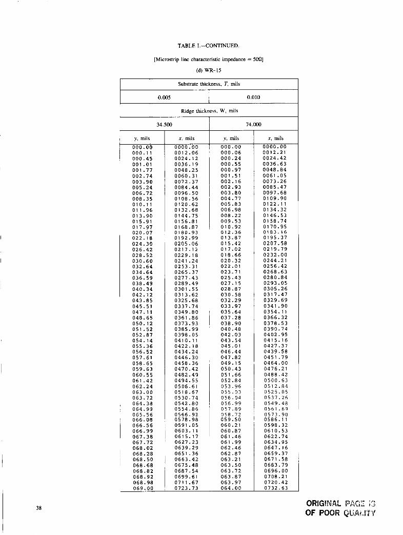
TABLE 1.-CONTINUED.
[Microstrip line characteristic impedance = 50Q]
(d) WR-15
Substrate thickness, T, mils
0.005 0.010 I Ridge thickness, W, mils
34.500
y . mils 000.00 000.11 000.45 001.01 001.77 002.74 003.90 005.24 006.72 008.35 010.11 01 1.96 013.90 015.91 017.97 020.07 022.18 024.30 026.42 028.52 030.60 032.64 034.64 036.59 038.49 040.34 042.12 043.85 045.51 047.11 048.65 050.12 051.52 052.87 054.14 055.36 056.52 057.61 058.65 059.63 060.55 061.42 062.24 063.00 063.72 064.38 064.99 065.56 066.08 066.56 066.99 067.38 067.72 068.02 068.28 068.50 068.68 068.82 068.92 068.98 069.00
x , mils 0000.00 0012.06 0024.12 0036.19 0048.25 0060.31 0072.37 0084.44 0096.50 01 08.56 0120.62 0132.68 0144.75 0156.81 0168.87 01 80.93 0192.99 0205.06 0217.12 0229.18 024 1 .24 0253.31 0265.37 0277.43 0289.49 0301.55 0313.62 0325.68 0337.74 0349.80 0361 -86 0373.93 0385.99 0398.05 0410.11 0422.18 0434.24 0446.30 0458.36 0470.42 0482.43 0494.55 0506.61 0518.67 0530.74 0542.80 0554.86 0566.92 0578.98 0591.05 0603.11 0615.17 0627.23 0639.29 0651.36 0663.42 0675.48 0687.54 0699.61 071 1.67
74.000
y . mils
000.00 000.06 000.24 000.55 000.97 001.51 002.16 002.93 003.80 004.77 005.83 006.98 008.22 009.53 010.92 012.36 013.87 015.42 017.02 018.66 020.32 022.01 023.71 025.43 027.15 028.87 030.58 032.29 033.97 035.64 037.28 038.90 040.48 042.03 043.54 045.01 046.44 047.82 049.15 050.43 051.66 052.84 053.96 055.03 056.04 056.99 057.89 958.12 059.50 060.21 060.87 061.46 061.99 062.46 062.87 063.21 063.50 063.72 063.87 053.97
0723.73 064.00
x , mils 0000 . oo 001 2.21 0024.42 0036.63 0048.84 0061.05 0073.26 0085.47 0097.68 0109.90 0122.11 01 34.32 0146.53 0158.74 0170.95 0183.16 01 95.37 0207.58 0219.79 0232.00 0244.21 0256.42 0268.63 0280.84 0293.05 0305.26 0317.47 0329.69 0341.90 0354.11 0366.32 0378.53 0390.74 0402.95 0415.16 0427.37 0439.58 0451 -79 0464.00 0476.21 0488.42 0500.63 0512.84 0525.05 0537.26 0549.48 0561 .69 0573.90 0586.11 0598.32 0610.53 0622.74 0634.95 0647. I6 0659.37 0671 .58 0683.79 0696.00 0708.21 0720.42 0732.63
38
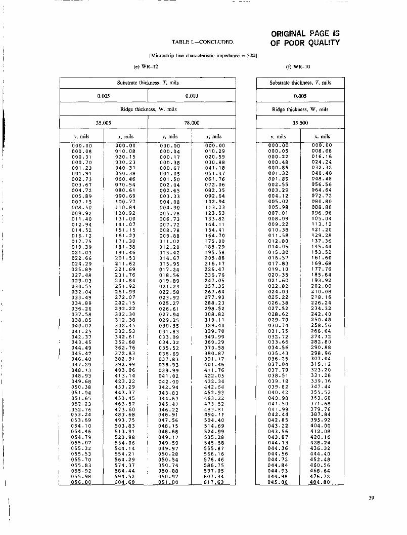
I
I
ORIGINAL PAGE IS TABLE 1.-CONCLUDED. OF POOR QUALITY
[Microstrip line characteristic impedance = son]
(e) WR-12
Substrate thickness, T, mils
0.005 I 0.010 ~ ~
Ridge thickness, W, mils
35.005
y , mils
000.00 000.08 000.31 000.70 001.23 001.91 002.73 003.67 004.72 005.89 007.15 008.50 009.92 01 1.40 012.94 014.52 016.12 017.75 019.39 021 -03 022.66 024.29 025.89 027.48 029.03 030.55 032 - 04 033.49 034.89 036.26 037.58 038.85 040.07 041.25 042.37 043.45 044.49 045.47 046.40 047.29 048.13 048.93 049.68 050.38 051.04 051.65 052.23 052.76 053.24 053.69 054.10 054.46 054.79 055.07 055.32 055.53 055.70 055.83 055.92 055.98 056.00
x, mils
000.00 010.08 020.15 030.23 040.31 050.38 060.46 070.54 080.61 090.69 100.77 110.84 120.92 131 .OO 141.07 151.15 161.23 171.30 181.38 191.46 201 -53 21 1.62 221.69 231.76 241.84 251.92 261.99 272.07 282.15 292.22 302.30 312.38 322.45 332.53 342.61 352.68 362.76 372.83 382.91 392.99 403.06 413.14 423.22 433.29 443.37 453.45 463.52 473.60 483.68 493.75 503.83 513.91 523.98 534.06 544.14 554.21 564.29 574.37 584.44 594.52
78.000
y , mils
000.00 000.04 000.17 000.38 000.67 001.05 001.50 002.04 002.65 003.33 004.08 004.90 005.78 006.73 007.72 008.78 009.88 01 1.02 012.20 013.42 014.67 015.95 017.24 018.56 019.89 021.23 022.58 023.92 025.27 026.61 027.94 029.25 030.55 031.83 033.09 034.32 035.52 036.69 037.83 038.93 039.99 041.02 042.00 042.94 043.83 044.67 045.47 046.22 046.91 047.56 048.15 048.68 049.17 049.59 049.97 050.28 050.54 050.74 050.88 050.97
604.60 , 051.00
x, mils
000.00 010.29 020.59 030.88 041.18 051.47 061.76 072.06 082.35 092.64 102.94 113.23 123.53 133.82 144.11 154.41 164.70 175.00 185.29 195.58 205.88 216.17 226.47 236.76 247.05 257.35 267.64 277.93 288.23 298.52 308.82 319.11 329.40 339.70 349.99 360.29 370.58 380.87 391.17 401.46 41 1.76 422.05 432.34 442.64 452.93 463.22 473.52 483.81 494.11 504.40 514.69 524.99 535.28 545.58 555.87 566.16 576.46 586.75 597.05 607.34 617.63
(f) WR-10
Substrate thickness, T, mils
0.005
Ridge thickness, W, mils
35.500
y , mils
000.00 000.05 000.22 000.48 000.85 001.32 001.89 002.55 003.29 004.12 005.02 005.98 007.01 008.09 009.22 010.38 011.58 012.80 014.05 015.30 016.57 017.83 019.10 020.35 021 -60 022.82 024.03 025.22 026.38 027.52 028.62 029.70 030.74 031.75 032.72 033.66 034.56 035.43 036.25 037.04 037.79 038.51 039.18 039.82 040.42 040.98 041.50 041 -99 042.44 042.85 043.22 043.56 043.87 044.13 044.36 044.56 044.72 044.84 044.93 044.98 045.00
x, mils 000.00 008.08 016.16 024.24 032.32 040.40 048.48 056.56 064.64 072.72 080.80 088.88 096.96 105.04 113.12 121.20 129.28 137.36 145.44 153.52 161.60 169.68 177.76 185.84 193.92 202.00 210.08 278.16 226.24 234.32 242.40 250.48 258.56 266.64 274 -72 282.80 290.88 298.96 307.04 315.12 323.20 331.28 339.36 347.44 355.52 363.60 371 -68 379.76 387.84 395.92 404.00 412.08 420.16 428.24 436.32 444.40 452.48 460.56 468.64 476.72 484.80
39

NASA National Aeronautics and
1. Report No.
NASA TP-2875
Report Documentation Page 2. Government Accession No.
7. Key Words (Suggested by Author@))
Monolithic microwave integrated circuits Waveguide-to-microstrip transitions Through-reflect-delay calibration technique
7. Author@)
Robert R. Romanofsky and Kurt A. Shalkhauser
18. Distribution Statement
Unclassified - Unlimited Subject Category 32
9. Performing Organization Name and Address
National Aeronautics and Space Administration Lewis Research Center Cleveland, Ohio 44135-3191
9. Security Classif. (of this report) 20. Security Classif. (of this page) 21. No of pages
Unclassified Unclassified 44
2. Sponsoring Agency Name and Address
National Aeronautics and Space Administration Washington, D.C. 20546-0001
22. Price’
A03
5. Supplemtntary Notes
3. Recipient’s Catalog No.
5. Report Date
March 1989 6. Performing Organization Code
8. Performing Organization Report No.
E-3983
10. Work Unit No.
506-44-20
11. Contract or Grant No.
13. Type of Report and Period Covered
Technical Paper
14. Sponsoring Agency Code
6. Abstra t
The jesign and evaluation of a novel fixturing technique for characterizing millimeter-wave solid-state devices is presented. The technique utilizes a cosine-tapered ridge guide fixture and a one-tier de-embedding procedure to produce accurate and repeatable device-level data. Advanced features of this technique include nondestructive testing, full waveguide bandwidth operation, universality of application, and rapid, yet repeatable, chip-level characterization. In addition, only one set of calibration standards is required regardless of the device geometry.