Embed Size (px)
Citation preview

Unit 2 : Combinational Circuit
Lesson 1 : Half and Full Adder Circuit
1.1. Learning Objectives
On completion of this lesson you will be able to :
♦ design half and full adder circuit
♦ understand basic operation of adder circuitry.
Digital computers and calculators perform various arithmetic operations
on numbers that are represented in binary form. These operations are all
performed in the arithmetic logic unit of a computer. Logic gates and
flip-flops are combined in the arithmetic logic unit so that they can add,
subtract, multiply and divide numbers. These circuits perform arithmetic
operations at speeds that are not humanly possible. We shall now study
the addition operation circuit which is an important arithmetic operation
in digital systems.
1.2. Binary Addition
1.2.1. The Half Adder
When two digits are added together, the result consists of two parts,
known as the SUM and the CARRY. Since there are only four possible
combinations of two binary digits, one combination produces a carry.
This can be shown as
0 1 0 1
+0 +0 +1 +1
Carry Sum Carry Sum Carry Sum Carry Sum
0 0 0 1 0 1 1 0
The truth table for the addition of two binary variables A and B can be
shown below.
A B Sum Carry
0
0
1
1
0
1
0
1
0
1
1
0
0
0
0
1
Table 2.1 : Half adder truth table.
From the truth table it is clear that the SUM is only produced when A is
at 1 and B is 0 or when A is 0 and B is 1. A CARRY is produced only
The Half Adder

Digital Systems and Computer Organization
42
when both A and B are at a logical 1. Hence the Boolean expression for
the SUM and CARRY output from the above truth table will be written
as follows :
SUM = A •B +A • B CARRY = A • B
Thus the logic circuit for a half adder will have two inputs, A and B and
two outputs, SUM and CARRY as shown in Fig. 2.1.
A
B
SUM
CARRY
Fig. 2.1 : SUM and CARRY
The sum can be easily generated by an Exclusive OR gate since
A ⊕ B= A •B +A • B
Consequently the resulting circuit is :
A
B
SUM
CARRY
Fig. 2.2 : SUM and CARRY
We have now a circuit which will perform binary addition. This circuit
is called a half adder circuit. Half adder circuit.
Thus the logic circuit for a
half adder will have two
inputs, A and B, and two
outputs, SUM and CARRY.

Combinational Circuit
43
1.2.2. The Full Adder
Computer performs the addition operation on two binary number at a
time, where each binary number can have several binary digits. The
addition process starts by adding the least significant bits (LSBS) of the
two numbers. For Example
01 0 1
+11 +1 +1
Carry Sum Carry Sum
0 1 1 0
1
Carry Sum
1 0
↓
= 1 0 0
At each step in this addition process we are performing the addition of 3
bits : two bits from two numbers and a CARRY in bit from previous
position. The result of the addition of these 3 bits produces 2 bits : a
SUM bit and a CARRY out bit. This CARRY would be added to the
next bit position. The same process is followed for each bit position.
Now we know the function of the full adder. So we can proceed to
design a logic circuit that will perform this function. First we shall
construct a truth table for such a circuit. Here, the SUM and CARRY
outputs result from the addition of inputs A, B and the CARRY IN.
A B C
(Carry in)
S
(Sum)
Carry out
0
0
0
0
1
1
1
1
0
0
1
1
0
0
1
1
0
1
0
1
0
1
0
1
0
1
1
0
1
0
0
1
0
0
0
1
0
1
1
1
F A
SUM
CARRY
B
A
C
Table 2.2 : Full adder truth table.
There are eight possible cases for three inputs and for each case the
desired output values are listed. For example, consider the case A = 1, B
= 0 and C = 1. The full adder (abbreviated FA) must add these bits to
produce a sum of 0 and a carry out of 1.
Since there are two output, we will design the circuitry for each output
individually, starting with the s output. The truth table 2.2 shows that
A truth table for full adder.
The Full Adder

Digital Systems and Computer Organization
44
there are four cases where s is to be a 1. Using the sum-of products
method, we can write for the expression as,
S = AB C +A BC + ABC + ABC
We shall now try to simplify this expression by factoring. Unfortunately,
none of the terms in the expression has two variable in common with any
of the other terms. However, A can be factored from the first two terms
and A can be factored from the last two terms :
S = A (BC + BC ) + A(BC + BC )
The first term in parentheses should be recognized as the exclusive OR
combination of B and C This can be written as B C. The second term in
the parenthesis should be recognized as the exclusive NOR of B and C
And this can be written as B ⊕ C . Thus the expression for S becomes.
S = A ( B ⊕ C ) + A ( B ⊕ C )
Let us take X = B ⊕ C. Then above equation can be written as,
S =A X + AX = A ⊕ X
Which is simply the Ex-OR of A and X. Replacing the expression for X,
we have
S = A ⊕ [B ⊕ C] (1)
Consider now the output carry out in the truth table 2.2. We can write
the sum-of -products expression for carry out as follows :
Carry out = AB C + AB C + A BC + A B C
This expression can be simplified by factoring. We will employ a trick
by using ABC term three times in this expression. This is, because it has
common factors with each of the other terms. Hence,
Carry out = A B C +AB C + A B C + AB C + A B C + A BC
= B C ( A +A ) + A C (B + B ) + A B (C +C) = B C + A C + A B (2)
This expression cannot be simplified further. Expressions (1) and (2) can
be implemented as shown in Fig. 2.3. The complete circuit with inputs
A, B and C and outputs S and carry out represents the full adder. The expression for CARRY
The expression for SUM.

Combinational Circuit
45
A
B
C
SUM
CARRY OUT
Fig. 2.3 : Complete circuitry of a full adder.
A full adder circuit can be constructed using two half adders. Two of the
three inputs are connected to the first half adder which produces a partial
sum and partial carry output. The partial sum is fed to the second half
adder along with the third of the original inputs. This causes the final
sum to be produced and also another partial carry.
SUM
CARRY OUT
Partial carryPartial sum
Partial carry
C
A
B
1st half adder 2nd half adder
Fig. 2.4 : A full adder circuit using half adder.
This partial carry combines with the other partial carry and gives the
final carry output. The three inputs to such a full adder, A,B and C are
completely interchangeable.
A full adder circuit
constructed by using two
half adder circuit.

Digital Systems and Computer Organization
46
1.3. Exercise
1.3.1. Multiple choice Question
a) How many inputs does a full adder have?
i) 1
ii) 2
iii) 3
iv) 4.
1.3.2. Questions for short answers
a) Write down the truth table for a half adder.
b) Derive the logic circuit from the truth table of a half adder.
c) Draw a full adder circuit by using two half adder.
1.3.3. Analytical question
a) Design and construct a logic circuit which will operate as a full
adder.

Combinational Circuit
47
Lesson 2 : Parallel Adder
2.1. Learning Objectives
On completion of this lesson you will be able to :
♦ know about the parallel addition process of binary numbers using
logic circuits
♦ design and construct a BCD adder.
So far, the circuits that have been dealt with have only been capable of
performing the additions for one digit positions of a binary number.
However there will generally be more than just one digit in the numbers
to be operated upon. There are two basic methods of using the logic
circuits to add multidigit numbers. One method is using what is called a
Serial system, the other is a Parallel system.
Serial addition is performed one bit at a time in a fixed time sequence,
using only a single full adder circuit. The addition starts with the least
significant bit (LSB), progressing to the most significant bit (MSB), the
numbers being stored in registers. A register is a short term memory
device capable storing a specified amount of data.
2.2. Parallel Adders
Parallel addition is the second of the two basic methods by which binary
numbers may be added using logic circuits. In a parallel addition system
all the bits of multidigit numbers are added simultaneously, hence the
name parallel addition Fig. 2.5 shows a 4-bit parallel adder system. One
full adder is provided for every bit to be added. Consequently, the time
taken for an addition is much less than that for a serial addition of the
same numbers. If the data is held in two registers A and B, then the
complete contents of these registers are applied simultaneously to the
respective A and B inputs of the full adders. The SUM output of each
adder is routed to the appropriate bit of the SUM register. The time
taken for the complete addition is slightly longer than that for a single bit
addition due to the propagation time of the carry from the least
significant to the most significant bit. When the data is presented to the
adders, the least significant bit of both A and B produce a CARRY bit,
either 0 or 1, which occurs a finite time, the population time, after the
initial presentation of the data to the adder. This carry information is
passed to the CARRY input of the next stage. The output from this
second stage will not be valid until the CARRY input information is
established. The same argument applies for all the subsequent stages of
the addition.
In a parallel addition system
all the bits of multidigit
numbers are added
simultaneously.
Digital Systems and Computer Organization
48
The overall speed advantage of parallel addition over the serial method
has already been mentioned. However, there is a disadvantage in that a
great deal of logic is required, especially if the numbers to be added
contain a lot of bits. A compromise is usually arrived at between the
speed advantage of the parallel system and the circuit cost advantage of
the serial system. The compromise is often in the form of a bit-parallel,
word-serial approach.
MSB LSB
SUM Register
A4
A3
A2
A1
MSB LSB
B Register
A4
A3
A2
A1
A B Ci
FULL
ADDER
Co SUM
A B Ci
FULL
ADDER
Co SUM
A B Ci
FULL
ADDER
Co SUM
A B Ci
FULL
ADDER
Co SUM
MSB LSB
A Register
CARRY IN
CARRY IN
Fig. 2.5 : The 4-bit parallel adder system.
The timing diagram for the 4-bit parallel adder is shown below :
In parallel adder a great
deal of logic is required

Combinational Circuit
49
Data to
Adder
1
0
1
0
1
0
1
0
1
0
1
0
Co1
Co2
Co3
Co4
Valid SUM
td
td
td
td
ta
Fig. 2.6 : The timing diagram for the 4-bit parallel adder.
td is the propagation delay time o each full adder, i.e. the time taken to
generate a valid output from each stage. ta is the time taken to generate a
valid SUM output from all stages from the time data is first applied to
the adder.
A refinement of the parallel adder shown on Fig. 2.7 is to dispense with
the SUM register and feed the sum data back to either the A or B
register. however, the sum must not be entered to the register until the
carry information has rippled through to produce a correct result,
otherwise relevant data may be corrupted.
The timing diagram for the
4-bit parallel adder.

Digital Systems and Computer Organization
50
MSB LSB
B and SUM Register
MSB LSB
A Ci
FULL
ADDER
Co S B
A Ci
FULL
ADDER
Co S B
A Ci
FULL
ADDER
Co S B
A Ci
FULL
ADDER
Co S B
A Register
CARRY IN
CARRY OUT
Fig. 2.7 : Schematic diagram of parallel adder.
2.3. Integrated Circuit Parallel Adder
Several parallel address are available as Integrated Circuits (ICs). The
most common is a 4-bit parallel adder IC that contains four
interconnected full adders. The 7483A, 74LS83A, and 74LS83A are all
TTL 4-bit parallel adder chips.
Cascading Parallel Adders
Two or more parallel-adder blocks can be connected (cascaded) to
accommodate the addition of larger binary numbers. Two 74LS83 adders
can be connected to add two 8-bit numbers. The adder on the right adds
the four least significant bits of the numbers. The C4 output of this adder
is connected as the input carry to the first position of the second adder,
which adds the four most significant bits of the numbers.
The eight sum outputs represent the resultant sum of the two 8-bit
numbers. C8 is the carry out of the last position (MSB) of the second
adder. C8 can be used as a carry into another adder stage if larger binary
numbers are to be handled.
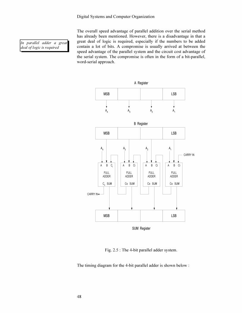
Problem
Determine the logic levels at the inputs and outputs of the 8-bit adder
when 7310 is added to 13810.
Two or more parallel-adder
blocks can be connected
(cascaded) to accommodate
the addition of larger binary
numbers.
Combinational Circuit
51
Solution
First convert each number to an 8-bit binary number :
138 = 10001010
73 = 01001001
These two binary values will be applied to the A and B inputs; that is,
the A inputs will be 10001010 from left to right, and the B inputs will be
01001001 from left to right. The adder will produce the binary sum of
the two numbers :
[A] = 10001010
[B] = 01001001
[S] = 11010011
The sum outputs will read 11010011 from left to right. There is no carry
into the C8 bit, and so it will be a 0.
2.4. Binary Coded Decimal ADDER
The binary coded decimal addition process is illustrated below :
1. Add the BCD code groups for each decimal digit position; use
ordinary binary addition.
2. For those positions where the sum is 9 or less, the sum is in proper
BCD form and no correction is needed.
3. When the sum of two digits is greater than 9, a correction of 0110
should be added to that sum to produce the proper BCD result. This
will produce a carry to be added to the next decimal position.
A BCD adder circuit must be able to operate in accordance with the
above steps. In other words, the circuit must be able to do the following :
1. Add two 4-bit BCD code groups, using straight binary addition. 2. Determine if the sum of this addition is greater than 1001 (decimal
9); if it is, add 0110 (6) to his sum and generate a carry to the next
decimal position.
The first requirement is easily met by using a 4-bit binary parallel adder
such as the 74LS83 IC. For example, if the two BCD code groups
represented by, A3A2A1A0 and B3B2B1B0 , respectively, are applied to a
4-bit parallel adder, the adder will perform the following operation :
A3A2A1A0 ← BCD code group
+ B3B2B1B0 ← BCD code group
S4S3S2S1S0 ← straight binary sum
S4 is a actually C4, the carry out of the MSB.
BCD ADDER

Digital Systems and Computer Organization
52
The sum outputs S4S3S2S1S0 can range anywhere from 00000 to 10010.
The circuitry for a BCD adder must include the logic needed to detect
whenever the sum is greater than 01001, so that the correction can be
added in. These cases where the sum is greater than 01001 are listed in
Table 2.3. Let’s define X. as a logic output that will go HIGH only when
the sum is greater than 01001. If we examine these cases, it can be
reasoned that X will be HIGH for either of the following conditions.
S4 S3 S2 S1 S0
0
0
0
0
0
0
1
1
1
1
1
1
1
1
1
0
0
0
0
0
1
1
1
1
0
0
0
1
1
0
0
1
1
0
0
1
0
1
0
1
0
1
0
1
0
(10)
(11)
(12)
(13)
(14)
(15)
(16)
(17)
(18)
Table 2.3.
1. Whenever S4 = 1 (sums greater than 15)
2. Whenever S3 = 1 and either S2 or S1 or both are 1 (sums 10 to 15)
This can be expressed as
X = S4 + S2 (S2 + S1)
Whenever X = 1, it is necessary to add the correction 0110 to the sum
bits and to generate a carry. Fig. 2.8 shows the complete circuitry for a
BCD adder, including the logic-circuit implementation for X.

Combinational Circuit
53
4- bit
Parallel Adder (74LS83)
4- bit
Parallel Adder (74LS83)
C4
C4
Not used
S3 S
2 S
1 S
0 A
3 A
2 A
1 A
0S
4
X
Carry to next
BCD adder
C0=0
C0
carry from
lower position
adder
B3 B
2 B
1 B
0
BCD
code
group
BCD
code
group
E3
E2
E1
E0
BCD sum
Fig. 2.8 : A BCD adder contains two 4-bit adders and c0orrection-
deterctor circuit.
The circuit consists of three basic parts. The two code groups A3A2A1A0
and B3B2B1B0 are added together in the upper 4-bit adder to produce the
sum S4S3S2S1S0. The logic gates implement the expression for X. The
lower 4-bit adder will add the correction 0110 to the sum bits only when
X = 1, producing the final BCD sum output represented by ∑3∑2∑1∑0 .
X is also the carry output that is produced when the sum is greater than
01001. Of course, when X = 0, there is no carry and no addition of 0110.
In such case, ∑3∑2∑1∑0 = S3S2S1S0.
To help in the understanding of the BCD adder, the reader should try
several cases by following them through the circuit. The following cases
would be particularly instructive.
Inputs
(a) [A] = 0101, [B] = 0011, C0 = 0
(b) [A] = 0111, [B] = 0110, C0 =0
Outputs
(a) [S] = 01000, X = 0, [∑] = 1000, CARRY = 0 (b) [S] = 01101, X = 1, [∑] = 0011, CARRY = 1
BCD adder circuit consists
of three basic parts.

Digital Systems and Computer Organization
54
2.5. Cascading BCD Adders
When decimal numbers with several digits are to be added together, it is
necessary to use a separate BCD adder for each digit position. The A
register contains 12 bits, which are the three BCD code groups for one of
the three-digit decimal numbers; similarly, the B register contains the
BCD representation of the other three-digit decimal number. The code
groups A3-A0 and B3-B0 representing the least significant digits are fed
to the first BCD adder. This first BCD adder produces sum outputs
∑3∑2∑1∑0 which is the BCD code for the least significant digit of the
sum. It also produces a carry output that is sent to the second BCD
adder, which is adding A7 through A4 and B7 through B4, the BCD code
groups for the second-decimal-digit position. The second BCD adder
produces∑7∑6∑5∑4, the BCD code for the second digit of the sum, and
so on. This arrangement can, of course, be extended to decimal numbers
of any size.
2.6. Exercise
2.6.1. Multiple choice questions
a) In a parallel addition system all the bits of multidigit numbers
are added
i) one bit at a time
ii) 4 bit at a time
iii) simultaneously
iv) none of above.
b) 74LS83 4-bit parallel contains following number of inter
connected full adder.
i) 1
ii) 2
iii) 4
iv) 16.
2.6.2. Questions for short answers
a) What is the basic difference between parallel adder and serial
adder?
b) Draw the timing diagram of a 4-bit parallel adder.
2.6.3. Analytical questions
a) Design 16-bit parallel adder using 74LS83 4-bit parallel adder.
b) Construct BCD adder using 4-bit binary parallel.
Cascading BCD Adders

Combinational Circuit
55
Lesson 3 : Multiplexer
3.1. Learning Objectives
On completion of this lesson you will be able to :
♦ understand the operation of multiplexer circuit at the gate level
♦ use multiplexer circuits in digital circuits.
3.2. Multiplexers (Data Selectors)
A digital multiplexer or data selector Multiplexer is a logic circuit that
accepts several digital data inputs and selects one of them at a time to
pass on to the output. Thus multiplexer transmits several signals on the
same line. The purpose of the multiplexer is to save on the number of
wires/lines needed to transmit data from multiple sources.
Fig. 2.8 shows the functional diagram of a general digital multiplexer
(MUX).
I0
I1
I2
IN
Z
Output
SELECT
Inputs
DATA
Inputs
Fig. 2.8 : Multiplexer.
The wide arrow indicates that they may actually be more than one signal
line. The multiplexer acts like a rotary switch connecting one of several
inputs to a single output. The selection of which input to connect to the
output is determined by additional inputs called SELECTOR control
lines. For example, output Z will equal data input I0 for some particular
SELECT input code, Z will equal I1 for another particular SELECT
input code; and so on. Thus, a multiplexer selects 1 out of N input data
sources and transmits the selected data to a single output chancel. This is
called multiplexing.
The selection of which input
to connect to the output is
determined by additional
inputs called SELECTOR.
Multiplexer is a logic circuit
that accepts several digital
data inputs and selects one
of them at a time.

Digital Systems and Computer Organization
56
3.3. Basic Two-Input Multiplexer
Fig. 2.9 shows the logic circuitry for a two-input multiplexer with data
inputs I0 and I1 and SELECT input S.
1
2
S
SELECT input
I0
I1
Z
S Output
0
1
Z = I0
Z = I1
Fig. 2.9 : Two-input multiplexer.
The logic level applied to the S input determines which AND gate is
enabled so that its data input passes through the OR gate to output Z.
Looking at it another way, the Boolean expression for the output is
Z = I0S + I1 S
With S = 0, this expression becomes
Z = I0 • 1 + I1 • 0 = I0 [ Gate 1 enabled]
which indicates that Z will be identical to input signal I0.
With S = 1, the expression becomes
Z = I0 • 0 + I1 • 1 = I1 [ Gate 2 enabled]
showing that output Z will be identical to input signal I1. The two input
multiplexer is referred to as a 2-to-1 mux.
3.4. Four-Input Multiplexer
The four input multiplexer is shown in Fig. 2.10, that selects one of four
inputs to connect to the output. This is referred to as a 4-to-1 mux. To
Two -Input Multiplexer
Four -Input Multiplexer

Combinational Circuit
57
select one of the four inputs, there must be four unique combinations of
the select lines. This requires two select lines providing the four unique
combinations 00, 01, 10, 11. A select line combination of 00 would
select input I0 select-line combination 01 would select input I1 and so on.
The table in the figure gives the outputs Z as a function of the select line
inputs. The Boolean expression for the output is,
Z = I0S0S1 + I1 S0S1 + I2S0 S1 + I3 S0 S1
Z
I0
I1
I2
I3
S1
S0
S1 S0 Z
0
0
1
1
0
1
0
1
I0
I1
I2
I3
Fig. 2.10 : 4-to-1 Multiplexer Implemantation.
A multiplexer is typically shown in a circuit as a single functional unit,
not as the gates comprising the circuit. A typical representation of a
4-to-1 multiplexer is shown in Fig. 2.11.

Digital Systems and Computer Organization
58
4-to-1
MUX
I0
I1
I2
I3
S1
S0
Z
Fig. 2.11 : 4-to-1 Multiplexer representation.
Since the multiplexer function is so useful, many TTL chips exist that
perform the equivalent operation of the circuit as shown in Fig. 4 (4-to-1
Mux figure). For example, the 74153 contains two 4-to-1 multiplexers,
the 74151 contains one 8-to-1 multiplexer and the 74157 contains four 2-
to-1 multiplexer.
3.5. Eight -Input Multiplexer
Fig. 2.12 shows the logic diagram for the 74151 eight-input multiplexer.
E E
I0 I
1 I
2 I
3 I
4 I
5 I
6 I
7
Fig. 2.12 : Logic Diagram for 74151 Multiplexer.
Eight -Input Multiplexer

Combinational Circuit
59
Inputs Outputs
E S2 S1 S0 Z Z
1 X X X 1 0
0 0 0 0 I0 I0
0 0 0 1 I1 I1
0 0 1 0 I2 I2
0 0 1 1 I3 I3
0 1 0 0 I4 I4
0 1 0 1 I5 I5
0 1 1 0 I6 I6
0 1 1 1 I7 I7
Table 2.4
This multiplexer has an enable input,E and provides both the normal
and inverted outputs. WhenE=0, the select inputs S2S1S0 will select one
data input (from I0 through I7) for passage to output Z. WhenE=1, the multiplexer is disabled so that Z = 0 regardless of the select input code.
This operation is summarizer in the truth table.
Problem 1
The circuit in Fig. 2.13 uses two 74151, an INVERTER, and an OR
gate. Describe the operation of this circuit.
74151
MUX
74151
MUX
X
S3
S2
S1
S0
Data
in
Data
in
Z
Z
I7
.
.
.
.
.
.
.
I0
E
S2
S1
S0
I7
.
.
.
.
.
.
.
I0
E
S2
S1
S0
Fig. 2.13 : Two 71151s combined to form a 16-input multiplexer.
This multiplexer has an
enable input,E and
provides both the normal
and inverted outputs.
Digital Systems and Computer Organization
60
Solution
This circuit has a total of 16 data inputs, eight applied to each
multiplexer. The two multiplexer outputs are combined in the OR gate to
produce a single output X. The circuit functions as a 16-input
multiplexer. The four select inputs S3S2S1S0 will select one of the 16
inputs to pass through to X.
The S3 input determines which multiplexer is enabled. When S3=0, the
top multiplexer is enabled, and the S2S1S0 inputs determine which of its
data inputs will appear at its output and pass through the OR gate to X.
When S3=1, the bottom multiplexer is enabled and the S2S1S0 inputs
select one of its data inputs for passage to output X.
3.6. Multiplexer Applications
Multiplexer circuits find numerous and varied applications in digital
system. These applications include data selection data routing operation
sequencing, parallel-to, serial conversion, waveform generation and
logic function generation. Some of them are discussed bellow.
Parallel -to-Serial Conversion
Many digital systems process binary data in parallel form because it is
faster. When data are to be transmitted over relatively long distances,
however, the parallel arrangement is undesirable because it requires a
large umber of transmission lines. For this reason, binary data or
information in parallel form is often converted to serial form before
being transmitted to a remote destination. A multiplexer is used for
performing such an operation.
Logic Function Generation
Multiplexers can be used to implement logic function directly form a
truth table. When used for this purpose the select inputs are used as the
logic variables and each data input is connected permanently HIGH or
LOW as necessary to satisfy the truth table.
Multiplexer Applications
The two multiplexer outputs
are combined in the OR gate
to produce a single output.
Multiplexers can be used to
implement logic function
directly form a truth table.

Combinational Circuit
61
74151 MUX
1Kohm
+Vcc
I0 I
1 I
2 I
3 I
4 I
5 I
6 I
7E
S0
S1
S2
A
B
C
Z = ABC + ABC + ABC
Input
logic
variables
Fig. 2.14: Logic function generation using MUX IC.
C B A Z
0 0 0 0
0 0 1 0
0 1 0 1
0 1 1 1
1 0 0 0
1 0 1 0
1 1 0 0
1 1 1 1
Table 2.5.
Fig. 2.14 shows an eight input multiplexer used to implement the logic
circuit that satisfies the given truth table 2.5. The input variables A,B,C
are connected to S0, S1, S2 respectively. According to the truth table, Z is
supposed to be LOW when CBA = 000. Thus multiplexer input I0 should
be connected LOW. Likewise, Z is suppose to be LOW for CBA = 001,
100, 101 and 110 so that inputs I1, I4, I5, and I6 should also be connected
LOW. The other sets of CBA conditions must produce Z = 1, and so
multiplexer inputs I2, I3 and I7 are connected permanently HIGH.
Thus the logic function implemented by multiplexer can be algebraically
expressed as
Z =A BC + A BC +ABC

Digital Systems and Computer Organization
62
3.7. Exercise
3.7.1. Multiple choice question
a) How many select input does a 32-to-1 line Multiplexer have?
i) 4
ii) 5
iii) 6
iv) 7.
3.7.2. Questions for short answers
a) Define multiplexing.
b) What is the function of a multiplexer’s select inputs?
c) What are the uses of multiplexer?
3.7.3. Analytical questions
a) Draw and describe the operation of 8-to-1 multiplexer.
b) Design a 16-to-1 line multiplexer using two 8-to-1 line
multiplexer.
c) How multiplexer can be used to work like a logic function
generator? Give Example.

Combinational Circuit
63
Lesson 4 : Demultiplexer
4.1. Learning Objectives
On completion of this lesson, you will be able to :
♦ understand the operation of demultiplexer circuit at the gate level
♦ use demultiplexer circuits in digital circuits.
A multiplexer takes several inputs and transmits one of them to the
output. A demultiplexer performs the reverse operation. It connects one
input to one of several outputs. The output is selected via select lines.
Fig.2 .15 shows the functional diagram of a digital demultiplexer. The
wide arrows for inputs and outputs can represent one or more lines. The
select input code determines which output DATA will be transmitted. In
other words, the demultiplexer takes one input data source and
selectively distributes it to 1 of N output channels just like a
multiposition switch.
DATA input
SELECT inputs
O0
O1
ON
Fig. 2.15 : General Demultiplexer.
The most common use of a demultiplexer is as a decoder. In fact,
demultiplexers are typically referred to as decoders. To illustrate the
behavior of a demultiplexer, consider the operation of a demultiplexer
that connects one input to one of four outputs. This is referred to as a 1-
to-4 demultiplexer. Fig. 2.16 show its logic diagram.
The single data input line I is connected to all four AND gates, but only
one of these gates will be enabled by the SELECT input lines. For
example with S1S0=00 only AND gate O will be enabled and data input I
will appear at output O . Other SELECT codes cause input I to reach the
other outputs.
A demultiplexer performs the
reverse operation. It
connects one input to one of
several outputs.
The most common use of a
demultiplexer is as a
decoder.

Digital Systems and Computer Organization
64
The operation of this demultiplexer is illustrated in truth table 2.6.
0
1
3
2
O0
O1
O2
O3
S0
S1
I
DATA input
Fig. 2.16 : One to 4 line demultiplexer.
Select code Outputs
S1 S0 O3 O2 O1 O0
0 0 0 0 0 I
0 1 0 0 I 0
1 0 0 I 0 0
1 1 I 0 0 0
Table 2.6 : 1-to-4 Demultiplexer truth table.
The functions illustrated in Table 2.6 can be expressed algebraically as :
O0 = IS1S0
O1 = IS1 S0
O2 = I S1S0
O3 = I S1 S0
4.2. 1-Line-to-8-Line Demultiplexer
Fig. 2.17 shows the logic diagram for a demultiplexer that distrubutes
one input line to eight output lines. The single data input line I is
connected to all eight AND gates, but only one of these gates will be
enabled by the SELECT input lines. For example, with S2S1S0 = 000,
only AND gate 0 will be enabled, and data input I will appear at output
Algebraic expression of a 1-
to-4 demultiplexer

Combinational Circuit
65
O0. Other SELECT codes cause input I to reach the other outputs. The
truth Table 2.7 summarizes the operation.
0
1
2
3
4
5
6
7
S0
S1
S2
IData input
O0
O1
O2
O3
O4
O5
O6
O7
Fig. 2.17 : 1-line-to-8-line demultiplexer.
SELECT code OUTPUT
S2 S1 S0 O7 O6 O5 O4 O3 O2 O1 O0
0 0 0 0 0 0 0 0 0 0 I
0 0 1 0 0 0 0 0 0 I 0
0 1 0 0 0 0 0 0 I 0 0
0 1 1 0 0 0 0 I 0 0 0
1 0 0 0 0 0 I 0 0 0 0
1 0 1 0 0 I 0 0 0 0 0
1 1 0 0 I 0 0 0 0 0 0
1 1 1 I 0 0 0 0 0 0 0
Table 2.7
Demultiplexer Applications
Demultiplexer circuits have various application in digital system. These
applications include serial-to-parallel conversion, data routing address Demultiplexer Applications

Digital Systems and Computer Organization
66
decoding and also logic function generation. Serial-to-parallel
conversion method is discussed below.
Serial-to-Parallel Conversion
When data communication between two computers take place over long
distance than both parallel-to-serial and serial-to parallel conversion
methods are needed. Here multiplexer performs parallel-to-serial
conversion and demulliplexer performs serial-to-parallel conversion.
Consider a situation in which two 16-bit computers must communicate.
Multiplexer is used to select a single bit of the input word and a
demultiplexer is used to connect that data to the proper bit of the output
word. The inter word can be transmitted and received by sequencing the
select lines from 0 through 15. This technique is called multiplexing and
demultiplexing.
4.3. Exercise
4.3.1. Multiple choice question
a) How many select lines are required to design a 1-to-8 line
demultiplexer?
i) 3
ii) 4
iii) 6
iv) 8.
4.3.2. Questions for short answers
a) What is the difference between multiplexer and demultiplexer ?
b) Write down the uses of demultiplexer.
4.3.3. Analytical question
a) Explain the operation of a 1-to-18 line demultiplexer.
Demulliplexer performs serial-
to-parallel conversion.

Combinational Circuit
67
Lesson 5 : Decoder
5.1. Learning Objectives
On completion of this lesson you will be able to :
♦ design and implementation of various types of decoder and encoder
circuits
♦ understand the operation of decoder and encoder logic and use them
in different circuit application
♦ learn the operation of code converters and display drivers.
5.2. BCD-to-7 Segment Decoder/Driver
Digital circuits often “communicate” with the outside world via seven-
segment displays such as those found in your calculator. These displays
consist of seven individual LEDS and form the decimal characters 0
through 9 and some times hex characters A through F. By controlling
the current through each LED, some segments will be lighted and others
will be dark so that the desired character pattern will be generated.
5.3. DECODERS
A decoder is a logic circuit that accepts a set of inputs that represents a
binary number and activates only the output that corresponds to that
input number. The diagram for a general decoder is shown in Fig. 2.18
with N inputs and M outputs. Since each of the N inputs can be 0 or 1,
there are 2N possible input combinations or codes. For each of these
input combinations only one of the M outputs will be active (HIGH); all
the other outputs are LOW. Many decoders are designed to produce
active-LOW outputs, where only the selected outputs is LOW while all
others are HIGH. This would be indicated by the presence of small
circles on the output lines in the decoder diagram.
Decoder
A0
A1
A2
AN-1
O0
O1
O2
OM-1
M
outputN
intput
2N input codes Only one output is high
for each input code
Fig. 2.18 : General decoder diagram.
Some decoders do not utilize all of the 2N possible input codes but only
certain ones. For example, a BCD-to-decimal decoder has a 4-bit input
A decoder is a logic circuit
that accepts a set of inputs
that represents a binary
number and activates only
the output that corresponds
to that input number.

Digital Systems and Computer Organization
68
code and ten output lines that correspond to the ten BCD code groups
0000 through 1001. If any of the unused codes are applied to the input
none of the outputs will be activated.
5.4. 3 to 8 Line Decoder
Fig. 2.19 shows the circuitry for a decoder with three inputs and 23=8
outputs. It uses all AND gates, and so the outputs are active-HIGH. Note
that for a given input code, the only output which is active (HIGH) is the
one corresponding to the decimal equivalent of the binary input code
(e.g.; output O6 goes HIGH only when CBA=1102=610).
0
1
2
3
4
5
6
7
C
(MSB)
B
A
(LSB)
O0
O1
O2
O3
O4
O5
O6
O7
Fig. 2.19 : 3-line-to-8-line (or 1-of-8) decoder.
C B A O0 O1 O2 O3 O4 O5 O6 O7
0 0 0 1 0 0 0 0 0 0 0
0 0 1 0 1 0 0 0 0 0 0
0 1 0 0 0 1 0 0 0 0 0
0 1 1 0 0 0 1 0 0 0 0
1 0 0 0 0 0 0 1 0 0 0
1 0 1 0 0 0 0 0 1 0 0
1 1 0 0 0 0 0 0 0 1 0
1 1 1 0 0 0 0 0 0 0 1
Table 2.8.
3 to 8 Line Decoder

Combinational Circuit
69
This decoder can be referred to in several ways. It can be called a 3-line-
to 8-line decoder, because it has three input lines and eight output lines.
It could also be called a binary-to-octal decoder or converter because it
takes a 3-bit binary input code and activates the one of the eight (octal)
outputs corresponding to that code. It is also referred to as a 1-of-8
decoder, because only 1 of the 8 outputs is activated at one time.
ENABLE Inputs
Some decoders have one or more ENABLE inputs that are used to
control the operation of the decoder. For example, refer to the decoder in
Fig. 2.20 and visualize having a common ENABLE line connected to a
fourth input of each gate.
O0
O1
O2
O3
O4
O5
O6
O7
A2
A1
A0
(MSB)
E1
E2
E3
Fig. 2.20 : Logic diagram for 74LS138 decoder.
With this ENABLE line held HIGH the decoder will function normally
and the A,B, C inputs code will determine which output is HIGH. With
ENABLE held LOW, however, all the outputs will be forced to the
LOW state regardless of the levels at the A, B, C inputs. Thus, the
decoder is ENABLED only if ENABLE is HIGH.
Fig. 2.21 shows the logic diagram for the 74LS138 decoder, it has
NAND-gate out-puts, so that its outputs are active-LOW. Another
indication is the labeling of the outputs as07, 06, 05, and so on; overbar
indicates active-LOW outputs.
Decoder can be referred to
in several ways.
Some decoders have one or
more ENABLE inputs that
are used to control the
operation of the decoder.

Digital Systems and Computer Organization
70
74LS138
1-of-8 decoder
E1
E2
E3
A2
A1 A
0
O7
O6
O5
O4
O3
O2
O1
O0
Fig. 2.21 : logic diagram for the 74LS138 decoder
E1 E2 E3 Outputs
0 0 1 Enabled for A2A1A0
1 × × Disabled
× 1 × Disabled
× × 0 Disabled
Table 2.9
The input code is applied at A2, A1, and A0, where A2 is the MSB. With
three inputs and eight outputs, this is a 3-to-8 decoder or, equivalently, a
1-of-8 decoder.
InputsE1,E2 andE3 are separate enable inputs that are combined in the
AND gate. In order to enable the output NAND gates to respond to the
input code at A2A1A0, this AND gate output has to be HIGH. This will
occur only whenE1=E2= 0 and E3=1. E1 and E2 are active LOW,E3
is active HIGH. If one or more of the enable inputs is in its inactive state,
the AND output will be LOW, which will force all NAND outputs to
their inactive HIGH state regardless of the input code. This operation is
summarized in the truth Table 2.9. Recall that x represents the “don’t
care” condition.
5.6. Decoder Applications
Decoders are used whenever an output or group of outputs is to be
activated only on the occurrence of a specific combination of input

Combinational Circuit
71
levels. These input levels are often provided by the outputs of a counter
or register.
Decoders are widely used in the memory system of a computer. Decoder
responds to the address code input from the central processor to activate
the memory storage location specified by the address code.
5.7. BCD-TO-7-Segment Decoder/Drivers
Fig. 2.22 shows the segment patterns that are used to display the various
digits. For example, to display a “6,” the segments c, d, e , f, and g are
made bright while segments a and b are dark.
a
b
c
d
e
fg
(a)
(b)
Fig. 2.22 : (a) Seven-segment arrangement; (b) active segments for each
digit.
A BCD-to-7-segment decoder/driver is used to take a 4-bit BCD input
and provide the outputs that will pass current through the appropriate
segments to display the decimal digit. The logic for this decoder is more
complicated than those we looked at previously because each output is
activated for more than one combination of inputs. For example, the e
segment must be activated for any of the digits 0, 2, 6, and 8, which
means whenever any of the codes 0000, 0010, 0110, of 1000 occurs.
Fig. 2.23 shows a BCD-to-7-segment decoder/driver (TTL 7446 or 7447)
being used to drive a 7-segment LED readout. The anodes of the LEDs
are all tied to Vcc(+5V). The cathodes of the LEDs are connected
Decoders are widely used in
the memory system of a
computer.
A BCD-to-7-segment
decoder/driver is used to
take a 4-bit BCD input.

Digital Systems and Computer Organization
72
through current-limiting resistors to the appropriate outputs of the
decoder/driver. The decoder/driver has active-LOW outputs.
BCD-to
7-segment
Decoder
7446 or 7447A
B
C
D
BCD
Input
a
b
c
d
e
f
g
+Vcc
Common
anode
connections
(a)
(b)
Fig. 2.23 : (a) BCD-to-7- segment decoder/driver driving a common-
anode 7 -segment LED display; (b) segment patterns for different
input codes.
To illustrate the operation of this circuit, let us suppose that the BCD
input is D = 0, C =1, B = 0, A =1, which is BCD for 5. With these inputs
the decoder/driver outputs a, f, g, c and d will be driven LOW
(connected to ground), allowing current to flow through the a, f, g, c and
d LED segments and thereby displaying the number 5. the b and e outputs will be HIGH (open), so that LED segments b and e cannot
conduct.

Combinational Circuit
73
5.8. Exercise
5.8.1. Multiple choice question
a) To control the operation of the decoder there may be one or
more
i) enable inputs
ii) select inputs
iii) output lines
iv) none of above.
5.8.2. Question for short answer
a) What is the function of the enable inputs of a decoder?
5.8.3. Analytical questions
a) Construct a 1-of- 64 decoder using eight 1 of 4 decoder
(74LS138).
b) Design a BCD to decimal decoder.

Digital Systems and Computer Organization
74
Lesson 6 : 7- Segment Decoder
6.1. Learning Objectives
On completion of this lesson you will be able to :
♦ understand the operation of 7-segment decoder
♦ drive an LCD.
6.2. Liquid Crystal Displays
A light emiting diode (LED) display generates or emits light energy as
current is passed through the individual segments. A liquid crystal
display (LCD) controls the reflection of available light. LCDs have
gained wide acceptance because of their very low power consumption
compared to LEDs, especially in battery-operated equipment such as
calculators, digital watches, and portable electronic measuring
instruments. LEDs have the advantage of a much brighter display,
which, is easily visible in dark or poorly lit areas.
a
c
b
d
e
f
g
LCD display
Backplane
Incident
ambient
light
a
c
b
Backplane
(a) (b)
a
b
c
d
e
f
g
Fig. 2.24 : Liquid crystal display (a) basic arrangement; (b) applying a
voltage between segment and back plane.
Basically, LCDs operate from a low-voltage (typically, 3 to 15 V rms),
low-frequency (25 to 60 Hz) ac signal and draw very little current. They
are often arranged as 7-segment displays for numerical readouts as
shown in Fig. 2.24. The ac voltage needed to turn on a segment is
applied between the segment and the backplane, which is common to all
segments. The segment and backplane form a capacitor that draws very
little current as long as the ac frequency is kept low.
6.2.1. LCD Operation
When there is no difference in voltage between a segment and the
backplane, the segment is said to be nonactivated (OFF). Segment d, e, f,
An LED display generates or
emits light energy as current
is passed through the
individual segments.

Combinational Circuit
75
and g in Fig. 2.24 are OFF and will reflect incident light so that they
appear invisible against their background. When an appropriate ac
voltage is applied between a segment and the backplane, the segment is
activated (ON). Segments a, b, and c in Fig. 2.24 are ON and will not
reflect the incident light, and thus they appear dark against their
background.
6.2.2. Driving an LCD
An LCD segment will turn ON when an ac voltage is applied between
the segment and the backplane, and will turn OFF when there is no
voltage between the two. Rather than generating an ac signal, it is
common practice to produce the required ac voltage by applying out-
phase square waves to the segment and backplane. This is illustrated in
Fig. 2.25 for one segment.
Control
40 Hz signal Segment
Backplane
5V
0
Fig. 2.25 : Driving an LCD segment.
A 40-Hz square wave is applied to the backplane and the Other input to
the EX-OR is a CONTROL input that will control whether the segment
is ON or OFF.
When the CONTROL input is LOW, the EX-OR output will be exactly
the same as the 40-Hz square wave, so that the signals applied to the
segment and backplane are equal. Since there is no difference in voltage,
the segment will be OFF. When the CONTROL input is HIGH, the EX-
OR or output will be the INVERSE of the 40-Hz square wave, so that the
signal applied to the segment is out of phase with the signal applied to
the backplane. As a result, the segment voltage will alternately be
at + 5V and at -5V relative to the backplane. This ac voltage will turn
ON the segment.
This same idea can be extended to a complete 7-segment LCD display as
shown in Fig. 2.26. It takes the BCD input code and provides the outputs
to drive the LCD-segments directly.
An LCD segment will turn
ON when an ac voltage is
applied between the segment
and the backplane.

Digital Systems and Computer Organization
76
LCD display
Backplane
BCD-TO-
7-Segment
Decoder
40 Hz
a
b
c
d
e
f
g
D
C
B
A
Fig. 2.26 : Driving 7-segment LCD.
6.3. Exercise
6.3.1. Multiple choice questions
a) A BCD - to- 7 segment decoder has.
i) 4 input time and 8 output line
ii) 4 input time and 7 output line
iii) 8 input time and 4 output line
iv) 8 input time and 16 output line.
b) To drive an LCD segment we use
i) AND gate
ii) OR gate
iii) NOR gate
iv) XOR gate.
6.3.2. Question for short answer
a) How can we drive an LCD segment?
6.3.3. Analytical question
a) Describe the operation of an LCD.

Combinational Circuit
77
Lesson 7 : Encoders
7.1. Learning Objectives
On completion of this lesson you will be able to :
♦ understand the operation of encoder
♦ learn how priority encoder works.
Most decoders accept an input code and produce a HIGH (or LOW) at
one and only one output line. In other words, we can say that a decoder
identifies, recognizes or detects a particular code. The opposite of this
decoding process is called encoding and is performed by a logic circuit
called an encoder. An encoder has a number of input lines, only one of
which is activated at a given time, and produces an N-bit output code,
depending on which input is activated.
ENCODER
A0
A1
A2
A3
AM-1
ON-1
O3
O2
O1
O0
M inputs
only one
HIGH at a time
N - bit
outputs code
Fig. 2.27 : General diagram for a encoder.
Fig. 2.27 is the general diagram for an encoder with M inputs and N
outputs. Here the inputs are active - HIGH, which means they are
normally LOW.
We saw that a binary-to-octal decoder (3-line-to-8line decoder) accepts a
3-bit input code and activates one of eight output lines corresponding to
that code. An octal-to-binary encoder (8-line-to-3-line encoder) performs
the opposite function; it accepts eight input lines and produces a 3-bit
output code corresponding to the activated input. Fig. 2.28 shows the
logic circuit and truth table 2.10 for an octal-to-binary encoder with
active-LOW inputs.
An encoder has a number of
input lines, only one of
which is activated at a given
time.

Digital Systems and Computer Organization
78
A0
A1
A2
A3
A4
A5
A6
A7
O0
LSB
O1
O2
MSB
8
Inputs
Fig. 2.28 : 8-line-to 3-line encoder.
Inputs Outputs
A0 A 1 A 2 A 3 A 4 A 5 A 6 A 7 O2 O1 O0
× 1 1 1 1 1 1 1 0 0 0
× 0 1 1 1 1 1 1 0 0 1
× 1 0 1 1 1 1 1 0 1 0
× 1 1 0 1 1 1 1 0 1 1
× 1 1 1 0 1 1 1 1 0 0
× 1 1 1 1 0 1 1 1 0 1
× 1 1 1 1 1 0 1 1 1 0
× 1 1 1 1 1 1 0 1 1 1
Table 2.10.
By following through the logic, you can verify that a LOW at any single
input will produce the output binary code corresponding to that input.
For stance, a LOW at A3 (while all other inputs are HIGH) will produce
O2 = 0, O1 = 1, and O0 = 1, which is the binary code for 3. Notice that
A0 is not connected to the logic gates because the encoder outputs will
normally be at 000 when none of the inputs A1 to A9 is LOW. For
proper operation, only one input should be active at one time.
7.2. Priority Encoders
A modified version of the encoder circuit, called a priority encoder,
includes the necessary logic to ensure that when two or more inputs are
activated, the output code will correspond to the highest-numbered input.
Priority encoders is a
modified version of encoder

Combinational Circuit
79
For example, when both A3 and A5 are LOW, the output code will be
101 (5). Similarly, when A6 , A2 , and A0 are all LOW, the output code
is 110 (6). The 74148, and 74HC148 are all octal-to-binary priority
encoders.
7.3. 74147 Decimal-to-BCD Priority Encoder
Fig. 2.29 shows the logic symbol and truth table for the 74147
(74LS147, 74HC147), which functions as a decimal-to-BCD priority
encoder. It has nine active-LOW inputs representing the decimal digits 1
through 9, and produces the inverted BCD code corresponding to the
highest-numbered activated input.
74147
Decimal-to-BCD
priority encoder
A1
A2
A8
A9
O0
O1
O2
O3
MSB
Nine
Inputs
Inverted
BCD
Fig. 2.29 : 74147 decimal-to-BCD priority encoder.
A 1 A 2 A 3 A 4 A 5 A 6 A 7 A 8 A9 O3 O2 O1 O0
1 1 1 1 1 1 1 1 1 1 1 1 1
X X X X X X X X 0 0 1 1 0
X X X X X X X 0 1 0 1 1 1
X X X X X X 0 1 1 1 0 0 0
X X X X X 0 1 1 1 1 0 0 1
X X X X 0 1 1 1 1 1 0 1 0
X X X 0 1 1 1 1 1 1 0 1 1
X X 0 1 1 1 1 1 1 1 1 0 0
X 0 1 1 1 1 1 1 1 1 1 0 1
0 1 1 1 1 1 1 1 1 1 1 1 0
Table 2.11.
Let’s examine the truth Table 2.11 to see how this IC works. The first
line in the table shows all inputs in their inactive HIGH state. For this
condition the outputs are 1111, which is the inverse of 0000, the BCD
code for 0. The second line in the table indicates that a LOW at A9
regardless of the states of the other inputs, will produce an output code
of 0110, which is the inverse of 1001, the BCD code for 9. The third line
shows that a LOW at A8 , provided that A9 is HIGH, will produce an
Digital Systems and Computer Organization
80
output code of 0111, the inverse of 1000, the BCD code for 8. In a
similar manner, the remaining lines in the Table 2.11 show that a LOW
at any input, provided that all higher-numbered inputs are HIGH, will
produce the inverse of the BCD code for that input.
The 74147 outputs will be normally HIGH when none of the inputs are
activated. This corresponds to the decimal 0 input condition. There is no
A0 input, since the encoder assumes the decimal 0 input state when all
other inputs are HIGH. The 74147 inverted BCD outputs can be
converted to normal BCD by putting each one through an INVERTER.
7.4. Exercise
7.4.1. Analytical question
a) Draw 8 line to 3 line encoder what is the function of a priority
encoder.