Embed Size (px)
Citation preview
Unintentional high density p-type modulation doping
of a GaAs/AlAs core-multi-shell nanowire
J. Jadczak,†,∇ P. Plochocka,∗,† A. Mitioglu,† I. Breslavetz,¶ M. Royo,§ A. Bertoni,§
G. Goldoni,§ T. Smolenski,# P. Kossacki,# A. Kretinin,@ Hadas Shtrikman,@ and
D. K. Maude†
Laboratoire National des Champs Magnétiques Intenses, CNRS-UJF-UPS-INSA, 143, avenue de
Rangueil, 31400 Toulouse, Institute of Applied Physics, Academiei Str. 5, Chisinau, MD-2028,
Republic of Moldova, Laboratoire National des Champs Magnétiques Intenses,
CNRS-UJF-UPS-INSA, 25, avenue de Martyrs, 38042 Grenoble, Institute for Nanoscience,
CNR-NANO S3, via Campi 213/A, 41125 Modena, Italy, Departament de Química Física I
Analítica, Universitat Jaume I, Av. Sos Baynat s/n, 12080 Castelló, Spain, Department of Physics,
Informatics and Mathematics, University of Modena and Reggio Emilia, Italy, Institute of
Experimental Physics, Faculty of Physics, University of Warsaw, Hoza 69, 00-681 Warsaw,
Poland, Department of Condensed Matter Physics, The Weizmann Institute of Science, Rehovot
76100, Israel, and School of Physics and Astronomy, University of Manchester, UK
E-mail: [email protected]
1
arX
iv:1
404.
5781
v1 [
cond
-mat
.mes
-hal
l] 2
3 A
pr 2
014

Abstract
Achieving significant doping in GaAs/AlAs core/shell nanowires (NWs) is of considerable
technological importance but remains a challenge due to the amphoteric behavior of the dopant
atoms. Here we show that placing a narrow GaAs quantum well in the AlAs shell effectively
getters residual carbon acceptors leading to an unintentional p-type doping. Magneto-optical
studies of such a GaAs/AlAs core multi-shell NW reveal quantum confined emission. Theo-
retical calculations of NW electronic structure confirm quantum confinement of carriers at the
core/shell interface due to the presence of ionized carbon acceptors in the 1 nm GaAs layer in
the shell. Micro-photoluminescence in high magnetic field shows a clear signature of avoided
crossings of the n = 0 Landau level emission line with the n = 2 Landau level TO phonon
replica. The coupling is caused by the resonant hole-phonon interaction, which points to a
large 2D hole density in the structure.
Keywords: GaAs core/shell nanowires, 2D confinement, resonant phonon coupling.
Semiconductor nanowires (NWs) represent a rapidly expanding field of research largely due to
their great technological promise.1–5 For example, transistor action has been demonstrated using
carbon nanotubes and silicon nanowires,6,7 it has been suggested that indium phosphide nanowires
can be used as building blocks in nanoscale electronics,8 and doped radial core-multi-shell NWs
have good chances to find industrial applications as high efficiency solar cells.9–13 NWs with two
dimensional (2D) carriers localized at the core/shell interface offer new perspectives in quantum
∗To whom correspondence should be addressed†Laboratoire National des Champs Magnétiques Intenses, CNRS-UJF-UPS-INSA, 143, avenue de Rangueil, 31400
Toulouse‡Institute of Applied Physics, Academiei Str. 5, Chisinau, MD-2028, Republic of Moldova¶Laboratoire National des Champs Magnétiques Intenses, CNRS-UJF-UPS-INSA, 25, avenue de Martyrs, 38042
Grenoble§Institute for Nanoscience, CNR-NANO S3, via Campi 213/A, 41125 Modena, Italy‖Departament de Química Física I Analítica, Universitat Jaume I, Av. Sos Baynat s/n, 12080 Castelló, Spain⊥Department of Physics, Informatics and Mathematics, University of Modena and Reggio Emilia, Italy#Institute of Experimental Physics, Faculty of Physics, University of Warsaw, Hoza 69, 00-681 Warsaw, Poland
@Department of Condensed Matter Physics, The Weizmann Institute of Science, Rehovot 76100, Israel4School of Physics and Astronomy, University of Manchester, UK∇Institute of Physics, Wroclaw University of Technology, 50-370 Wroclaw, Poland
2
electronics.4 However, to introduce carriers the control and understanding of the doping mecha-
nisms in NWs is crucial.
Epitaxial GaAs has been investigated for more than 40 years, a field of research propelled by
the discovery of the quantum Hall effect with its panoply of exotic many body ground states.14,15
Significant efforts have been made to obtain high mobility 2D carriers in GaAs heterostructures
grown by molecular beam epitaxy (MBE). Notably, the development of remote or modulation
doping, which spatially separates the carriers from the dopant atoms, was a crucial step in the
discovery of the fractional quantum Hall effect.15 The direct application of the modulation dop-
ing techniques to GaAs/AlAs NWs would seem to be a natural evolution. Today high quality
GaAs/AlAs nanowires with a large aspect ratio and typical diameters of a few tens of nanometers
are routinely grown by MBE using the vapour-liquid-solid (VLS) method.16–24 While core multi
shell NWs would seem to be ideally suited for modulation doping, in practice achieving a signifi-
cant doping remains a challenge. In the VLS method, depending upon the growth plane, dopants
can act as donors or acceptors25 and the dopant incorporation can be different for axial and lateral
(sidewall) growth26 resulting in an inhomogeneous dopant distribution, or even compensation and
negligible doping.27 In NWs the use of the AlGaAs ternary alloy for the shell can lead to the segre-
gation of the Ga and Al atoms leading to the formation of the quantum dots.28,29 Moreover, using
AlGaAs for the shell leads to a red shift of the photoluminescence emission from the NW core,
which is not understood.30 On the other hand both experiment and theory suggest that modulation
doping in core-multi-shell NWs can lead to non uniform charge distribution with an accumulation
of charge at the facets or corners of the hexagonal NW which can lead to quantum confinement.31
In this work, we show that incorporating a narrow GaAs quantum well, which can be used to
accommodate dopants, in the AlAs shell of the NW can lead to significant unintentional p-type
doping due to the incorporation of residual carbon acceptors. Experiment and calculations demon-
strate that charge transfer at low temperature leads to quantum confinement with the formation of
a high density two dimensional hole gas at the core/shell interface of the NW.
The GaAs/AlAs NWs were grown by MBE using the self-assisted VLS method, on (111)-
3

Figure 1: (a) typical transmission electron microscopy (TEM) image taken from the center of aGaAs/AlAs core-multi-shell NW, (b)pure zinc blende structure confirmed by the electron diffrac-tion taken from the [011] direction, the arrow is aligned along the [111] growth direction, (c)scanning electron microscope (SEM) image of the GaAs/AlAs core-multi-shell NWs ∼ 11µmlong.
oriented silicon bearing a native oxide layer. After water removal at 200◦C, the Si wafer was
outgassed in a separate chamber (600◦C), before being transferred into the MBE growth chamber.
Growth was initiated by Ga condensation at pin holes in the SiO2 layer and carried out at 640◦C and
a group V/III (As4/Ga) ratio of 100. Uniform diameter GaAs NWs were grown with a high aspect
ratio, no significant tapering and pure zinc-blende structure, as revealed by careful transmission
and scanning electron microscopy (Fig. 1(a) and (c)) and electron diffraction taken from the [011]
direction (Fig. 1(b)). For growth of the shell (nominally AlAs 3 nm/GaAs 1 nm/ AlAs 3 nm) and
12 nm GaAs capping layer, the temperature was lowered to 520◦C. The hexagonal GaAs NW core
of side length d ' 22 nm composes a substrate for the multilayer structure, which consists of a
AlAs/GaAs/AlAs shell of a nominal thickness of 7 nm and a GaAs capping layer.
A typical µPL spectrum of a single core-multi-shell NW obtained in the absence of magnetic
field at a temperature T = 1.8 K is presented in Fig. 2 (see methods section for experimental
details). For comparison, we show a µPL spectrum measured on a single core-shell NW.32 The
structure of each sample is shown schematically in the inset of Fig. 2. We stress that both samples
were grown in the same MBE chamber under nominally the same growth conditions. Both NWs
have a rather large core (80 nm for core-shell and 60 nm for core-multi-shell) so that in a first
4
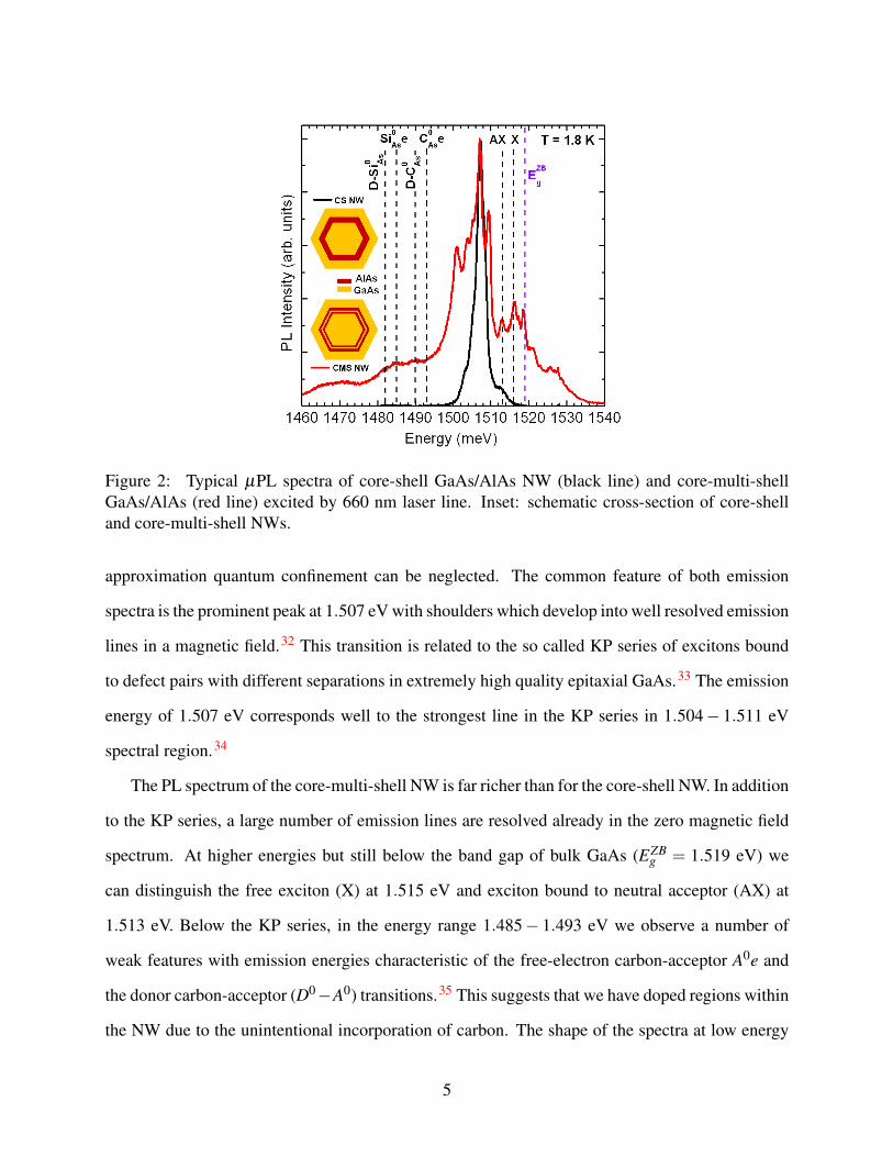
Figure 2: Typical µPL spectra of core-shell GaAs/AlAs NW (black line) and core-multi-shellGaAs/AlAs (red line) excited by 660 nm laser line. Inset: schematic cross-section of core-shelland core-multi-shell NWs.
approximation quantum confinement can be neglected. The common feature of both emission
spectra is the prominent peak at 1.507 eV with shoulders which develop into well resolved emission
lines in a magnetic field.32 This transition is related to the so called KP series of excitons bound
to defect pairs with different separations in extremely high quality epitaxial GaAs.33 The emission
energy of 1.507 eV corresponds well to the strongest line in the KP series in 1.504− 1.511 eV
spectral region.34
The PL spectrum of the core-multi-shell NW is far richer than for the core-shell NW. In addition
to the KP series, a large number of emission lines are resolved already in the zero magnetic field
spectrum. At higher energies but still below the band gap of bulk GaAs (EZBg = 1.519 eV) we
can distinguish the free exciton (X) at 1.515 eV and exciton bound to neutral acceptor (AX) at
1.513 eV. Below the KP series, in the energy range 1.485− 1.493 eV we observe a number of
weak features with emission energies characteristic of the free-electron carbon-acceptor A0e and
the donor carbon-acceptor (D0−A0) transitions.35 This suggests that we have doped regions within
the NW due to the unintentional incorporation of carbon. The shape of the spectra at low energy
5
is characteristic for p-doped structures, as recently observed for a single GaAs NW with an axial
heterojunction.36 In particular, it was shown that the emission energy for n-type and p-type material
is quite different; for p-type GaAs NWs the emission is dominated by recombination via acceptor
centers, whereas for n-type NWs emission is blue shifted with respect to the GaAs band gap due
to a band filling effect with increasing doping concentration.36,37
For the core-multi-shell NWs we observe additional emission lines at energies higher than the
band gap of GaAs in the range 1.520− 1.528 eV. This emission energy is typical for a GaAs
quantum well (QW) of width 15−20 nm38,39 suggesting a quantum confinement of the carriers in
the core. To distinguish this high energy emission from the emission in other spectral regions we
refer to it a “2D like” in the rest of the paper. The core-multi-shell structure incorporates a 1 nm
GaAs narrow quantum well in the AlAs shell at a distance of 3 nm from the core. No emission
from this ultra thin quantum well (QW) is detected at higher energies, presumably due to the rapid
thermalization (escape) of photo-created carriers. The 1 nm GaAs layer between the two AlAs
layers is expected to getter impurities, notably residual carbon atoms.40,41 It acts as an efficient
impurity trap due to the higher solubility of carbon atoms in GaAs and due to the floating of
carbon atoms at the AlAs vacuum interface during the MBE growth.40,41 Moreover, for AlAs we
expect the concentration of carbon to be quite high because Al atoms are more reactive with carbon
or other impurities.42 For example, the residual carbon incorporation in AlAs can be two orders
of magnitude higher than for GaAs.42 In our core-multi-shell NWs the carbon incorporated in the
GaAs quantum well can lead to a non-uniform charge distribution with excess holes accumulated
at the core/shell interface.
This hypothesis is confirmed by 3D self-consistent simulations of the NW electronic structure.
The modeling assumes spatial invariance along the NW axis and includes the nominal multi-shell
material modulation over the NW cross section. The interstitial GaAs quantum well is uniformly
doped with a constant density of acceptors δA. Our results predict that a hole gas starts to accumu-
late at the core/shell interface for p-doping densities of the order of 2.0×1019 cm−3 (corresponding
to a linear density of 4.63×107 cm−1 in the NW). The hole gas density distribution for a NW with
6

Figure 3: Calculated PL spectra (main panel) and hole gas distributions (small left panels) for core-multi-shell NWs with the p-doping densities ρA indicated in the left panels, together with the 2Dfree hole density Nh. The colormap insets illustrate the squared envelope functions for the electron(left) and hole (right) states whose recombination yields the PL peaks. The vertical dashed lineindicates the position of the GaAs bulk band gap.
three selected doping densities is illustrated in the left panels of Fig. 3. The different localization
patterns are in line with previous results.43 At low densities the hole gas is distributed near the
heterojunction forming six wide channels at the center of the hexagonal facets (bottom panel). As
the doping density is increased the hole gas moves closer to the heterojunction and it forms, first, a
quasi-uniform sixfold bent 2DEG (middle panel), and finally, six tunnel-coupled narrow channels
at the edges (top panel).
The calculated PL spectra corresponding to the same doping densities can be seen in the main
panel of Fig. 3. With increasing doping densities the exciton ground state red shifts and its intensity
is substantially reduced. This can be explained as follows: The peak red shifts due to the larger
attracting mean field experienced by the electron when the hole density is increased. At the same
time, whereas the hole ground state is further localized near the heterojunction, the electron ground
state remains in the center of the GaAs core (see two top-left insets in Fig. 3) due to the repulsive
potential generated by the high density of acceptors. Therefore, the overlap between the ground
electron and hole states becomes very small and the PL intensity of such transition is reduced. The
7

PL spectra of the NWs with higher acceptor densities show an additional intense peak at 1.529 eV.
As illustrated in the corresponding insets in Fig. 3, this peak originates from the recombination of
an electron in the ground state and a hole in an excited, but still occupied, state with an azimuthal-
like nodal surface. Since this hole state is well spread over the center of the GaAs core it has a
large overlap with the electron ground state leading to an intense peak in the PL spectrum. This
peak is not observed at lower doping density since the excited hole state is unoccupied.
Figure 4: Evolution of the PL spectra (solid curves) of core-multi-shell GaAs/AlAs NW as functionof the excitation power, at T= 1.8 K. The calculated PL spectra for different doping levels areplotted for comparison (dashed curves). The black dot-dashed lines are a guide to the eye tohighlight the evolution of the position of 2D emission lines described in the text. Note that thespectra have been shifted vertically for clarity.
The concentration of photo created electron hole pairs, and thus the concentration of holes can
also be tuned by varying the excitation power. A comparison between experimental results and
theoretical simulation is presented in Fig. 4, which shows plots of µPL spectra for different exci-
tation powers. The relative intensity of the KP series of lines, below EZBg = 1.519 eV, decreases as
the excitation power increases. This is due to the saturation of these transitions when all the defect
pairs have a bound exciton. In contrast, the 2D like emission intensity increases continuously with
excitation power. For the highest excitation power, the spectra are dominated by emission related
to the 2D hole gas. This further confirms the very different origins of each emission channel.
Theory predicts that the mechanism of the 2D recombination depends on the concentration
8

of photo-excited carriers. Increasing the number of photo created electron-hole pairs changes the
overlap between electron and ground hole states due to the modified distribution of 2D hole gas
in the core. The calculated PL spectra for two different hole concentrations are shown in Fig. 4
for comparison, showing qualitative agreement with the experimental data. The transition around
1.526 eV shifts toward lower energies with increasing excitation power, while the second peak
around 1.529 eV, originated from recombination of electrons with holes in excited state, remains
at the same energy. Its intensity is significantly enhanced as a straightforward consequence of the
increased occupation of the electron and hole sub-bands involved in the radiative recombination.
Figure 5: (a) Evolution of PL spectra of core-multi-shell GaAs/AlAs NW as a function of temper-ature, (b) Temperature dependence of the emission energy (symbols) together with the establishedtemperature dependence of the GaAs band gap (lines) (c) Integrated PL intensity rate ln(−1+I0/I)as function of 1/T (symbols). The lines are the linear fits used to deduce the activation energies.
The temperature dependence of the µPL spectra presented in Fig. 5 (a) provides further confir-
mation of the 2D character of the observed emission. In the µPL spectra at T=12 K, two relatively
broad peaks are observed corresponding to the recombination of the acceptor bound exciton (AX)
and the confined 2D exciton (X2D) at higher energies. Both shift to lower energy with increas-
9

ing temperature at a rate which tracks the temperature dependence of the GaAs band gap (see
Fig. 5 (b)). The emission intensity of AX, observed below EZBg , decreases much more rapidly than
the intensity of the confined exciton peak indicative of a distinctly different dissociation channel
for each transition. The thermal dissociation of excitons leads to a decrease in the normalized inte-
grated emission intensity I/I0 = 1+αe−E/kT .44 In order to estimate the activation energies associ-
ated with both processes, in Fig. 5 (b) we plot the integrated intensity rate ln(−1+ I0/I) as function
of 1/T . The slope of the linear fit to the data gives the activation energies E(AX) = 3.7 meV and
E(X2D) = 8.4 meV. The activation energy for AX coincides with the binding energy of the accep-
tor bound exciton in high purity GaAs44 and is also very close to the value reported earlier for ZB
GaAs NWs (4 meV).16 The twofold higher activation energy of X2D is expected for 2D confined
excitons further confirming the localization of holes on the facets.
In Fig. 6 the color plot shows differential µPL spectra, obtained by subtracting suitably av-
eraged spectra, in magnetic fields up to 22 T applied perpendicular to the core-multi-shell NW
growth axis. The PL emission lines sharpen and greatly increase in strength in a magnetic field,
which allows us to resolve many more features. On top of the color plot the symbols (white stars)
show the position of peaks manually identified for each spectra. This is useful to show weak fea-
tures, particularly at low magnetic fields. At high energies we predominantly observe two lines
corresponding to emission from quantum confined 2D carriers. At intermediate energies there is a
series of lines previously identified with the KP series related to excitons bound to closely spaced
defect pairs.32 At low energies, as we will later show, the observed lines can be identified with the
LO and TO phonon replicas of the 2D emission observed at high energies.
For all the lines, at low magnetic field, the emission energy increases quadratically due to
the diamagnetic shift. At higher magnetic field the dependence becomes linear in the Landau
quantization regime. The magnetic field dependence of the KP series of lines in an undoped NW
was discussed in detail in a previous publication.32 Here we focus on the lines linked to confined
carrier emission. The energy of emission as a function of magnetic field can be described by the
ground state of a 2D harmonic oscillator in perpendicular magnetic field,
10

Figure 6: Color plot showing differential µPL spectra of core-multi-shell GaAs/AlAs NW mea-sured as function of magnetic field. The excitation power was a few nW and the temperature of themeasurements was 1.7 K. The lines show the calculated evolution of the two high energy 2D emis-sion lines together with their LO (dashed lines) and TO (solid lines) phonon replicas as describedin the text. The observed avoided crossing is the result of resonant polaron coupling.
E(B) = E0 + h√
ω20 +(ωc/2)2 (1)
where ω0 is the harmonic trap frequency, which controls the diamagnetic shift and ωc = eB/m∗
is the cyclotron frequency. Here we neglect the Zeeman splitting which is not resolved in our
data. The LO and TO phonon replicas are given by E(B)− hωph where hωph is the LO or TO
phonon energy in GaAs with hωLO = 36.25 meV or hωTO = 33.29 meV.45 The 2D emission lines
are quite weak at low magnetic field and the lower line shows distinct evidence for an avoided
11

crossing around 12 T which makes it difficult to fit Eq.(1) to the data. Fortunately, the phonon
replicas have reasonable strength over a wide range of magnetic field allowing us to reliably extract
hω0 = 4.75 meV and m∗ = 0.087me. The second term in the Taylor expansion of Eq.(1) gives the
coefficient for the diamagnetic shift he2/8ω0m∗2 ' 50µeV/T2 which is reasonable for a confined
exciton.46
Avoided crossings in the emission from the lowest (n = 0) Landau level have previously been
observed in high density 2DEGs and are due to a resonant polaron coupling which occurs when
∆nhωc = hωLO.47 Occupancy arguments require that in order to observe such an effect the Fermi
energy should be similar to or greater than the phonon energy, which requires a high 2D carrier
density ≥ 1× 1012 cm−2. The avoided crossing behavior can be described using a perturbation
approach where the unperturbed energies are replaced by
E± =12
(E +En
ph
)± 1
2
√(E−En
ph)2−4γ2
ph (2)
where Enph is the energy of the nth phonon replica obtained from Eq.(1) with ωc/2→ (n+ 1
2)ωc
and γph is the characteristic interaction energy for each phonon. The evolution of the emission
lines, calculated using Eq.(2) and shown by the yellow lines in Fig. 6, is in good agreement with
our data, nicely reproducing the phonon replicas and the avoided crossing behavior observed in
the n = 0 Landau level. Note that as m∗ and ω0 were extracted from the unperturbed n = 0 phonon
replica the only fitting parameters are the characteristic interaction energies (γph) which we find
to be equal to γTO ' 4 meV and γLO ' 2 meV. The avoided crossing with the n = 1 phonon
replica exceeds our maximum magnetic field occurring for fields above 22 T. The observed avoided
crossing occurs between the n = 0 Landau level emission and the n = 2 Landau level phonon
replica. Moreover, the magnetic field position of the avoided crossing suggests that interaction
with the TO phonon dominates. The interaction with the LO phonon would lead to an avoided
crossing at higher magnetic field. This is further evidence for the 2D nature of the carriers involved
since coupling to the TO phonon mode is absent in 3D systems.48
In conclusion, we have carried out optical studies of the single GaAs/AlAs core-multi-shell NW
12
in high magnetic field. We have compared the obtained results with the typical spectra collected for
single GaAs/AlAs core-shell NW with comparable diameter. In the PL spectra of the core-multi-
shell NW we have observed emission above EZBg = 1.519 eV which is related to 2D confinement
of carriers in the core. Our results are in good agreement with theoretical calculations, which
predict different localization regimes for carriers as a function of doping. Moreover, in magneto-
PL spectra from core-multi-shell NWs we have observed avoided crossings of emission lines. The
underlying coupling is caused by the hole-phonon interaction in a 2D system with a dense gas.
This shows that the presence of 1 nm GaAs layer in the shell, which acts as an efficient impurity
trap, can lead to the efficient incorporation of residual acceptors (carbon) and the formation of a
dense 2D hole gas at the facets of the NW core.
Acknowledgement
We thank Ronit Popovitz-Biro for the careful TEM mesurements. This work was partially sup-
ported by the Region Midi-Pyrenées, the Programme Investissements d’Avenir under the program
ANR-11-IDEX-0002-02, reference ANR-10-LABX-0037-NEXT, ANR JCJC project milliPICS
and project APOSTD/2013/052 Generalitat Valenciana Vali+d Grant. G.G. and A.B. acknowledge
support from EU-FP7 Initial Training Network INDEX. G.G. acknowledges support from Univer-
sity of Modena and Reggio emilia, through grant ’Nano- and emerging materials and systems for
sustainable technologies’. We would also like to acknowledge partial support by the Israeli Science
Foundation grant #530/08 and Israeli Ministry of Science grant #3-6799.
Supporting Information Available
Experimental techniques
The study of the optical properties of core-multi-shell NW’s was carried out in two experimental
setups. For measurements of the micro-photoluminescence (µPL) in magnetic field the sample was
placed in a system composed of piezoelectric x-y-z translation stages and a microscope objective.
13

The µPL system was cooled to a temperature of T=1.8 K in a cryostat placed in a resistive magnet
producing magnetic fields of up to B = 22 T. The field was applied in the Faraday configuration,
perpendicular to the NW 〈111〉 growth axis. The sample was illuminated by a diode laser at 660
nm. Both the exciting and collected light were transmitted through a monomode fiber coupled
directly to the microscope objective. The diameter of the excitation beam on the sample was of
the order of 1 µm. The emission from the sample was dispersed in a spectrometer equipped with
a multichannel CCD camera. For additional µPL measurements in the absence of magnetic field,
the sample was placed in helium flow cryostat with optical access. The cryostat was mounted on
motorized x-y translation stages. The µPL was measured for temperatures varying from 10 to
100 K. Excitation and collection was implemented using a microscope objective with a numerical
aperture NA=0.66 and magnification ×50. The diameter of the excitation spot on the sample was
of the order of 1µm and the µPL spectra have been recorded using a spectrometer equipped with
a multichannel CCD camera.
Structural properties of the GaAs/AlAs/GaAs/AlAs/GaAs core/shell QW nanowires
We do not have a structural characterization of the exact NW investigated in our µPL set up. We
provide in this section structural characterization and direct evidence for the presence of a well-
defined QW within a very similar core multi shell structure grown in the same system and under
similar growth conditions and layer thicknesses. This sample was studied intensively by cross
sectional HR-TEM (prepared using FIB) as demonstrate in Figure 7. Figure 7(a) shows a HR-
TEM image taken on a cross section of the multi shell nanowire showing the two AlAs shell layers
(bright stripes) and a few monolayers thick GaAs QW embedded between them (GaAs core and
capping layer on the right and left hand sides, respectively, the scale bar is 5 nm. Figure 7(b) is a full
TEM image of the cross section taken from a core multi shell nanowire with very similar nominal
thicknesses as the ones studied in this work. Figure 7(c) shows the intensity profile showing clearly
the splitting of the AlAs layer into two layers, consistent with the presence of a thin GaAs QW in
between them.
14

Figure 7: (a) HR-TEM image taken on a cross section of the multi shell nanowire showing the twoAlAs shell layers (bright stripes) and a few monolayers thick GaAs QW embedded between them(GaAs core and capping layer on right and left hand sides, respectively, scale bar is 5 nm. (b) TEMimage of a cross section taken from a core multi shell nanowire. (c) intensity profile of the regionmarked on the cross section.
Self consistent calculation of the charge distribution
Calculations have been conducted within a standard envelope function approach, in a single-band
approximation. We consider the NW as a 3D system spatially invariant along the NW axis direction
z. This allows us to factorize the electron (hole) envelope functions as Ψe(h)nkz
(r,z) = ϕe(h)n (r)eikzz,
with parabolic energy dispersions, Ee(h)nkz
= εe(h)n ± h2k2
z2mz
e(h), in the in-wire momentum kz. Over the
r ≡ x,y plane, the NW cross section is hexagonal, and the material and doping modulations are
described in a corresponding hexagonal domain using a symmetry-compliant triangular grid. We
use an isotropic electron effective mass (mze = mr
e) but a highly anisotropic hole mass. Over the
in-plane direction we use the hole mass along the [110] direction which is much larger than the
hole mass that we use along the in-wire direction [111]. The ground state hole density nh(r) is
obtained through a Kohn-Sham LDA procedure.
The self-consistent potential VKS(r) =V (r)+VH(r)+VXC(r) includes the effect of the spatial
15

confinement V (r) determined by the materials band offset, the Hartree potential VH(r) generated
by free holes and static acceptors, and an approximate exchange-correlation potential VXC(r).49 In
our samples, conduction band electrons are generated by the laser pumping alone, thus they are
minority carriers with a low density: we solve the corresponding Schrödinger equation including
the electrostatic potential generated by the self-consistent hole density and the density of static
acceptors. In this way we take into account excitonic effects at a mean-field level. Further details
can be found in references.43,50
From the conduction and valence band states, we compute the PL spectra neglecting dynamic
screening effects and assuming that the photoexcited carriers relax to the lowest available state
before the radiative recombination. This means that electrons recombine from the lowest-lying
conduction states with holes in states lying above the Fermi level µ . The PL intensity is obtained
as
τ(ω)∝ ∑im|Sim|2
∫ dkz
2πf e(Ee
ikz,T )(1− f h(Eh
mkz−µ,T ))Γ(Ee
ikz−Eh
mkz− hω− γ), (3)
where
Sim =∫
drϕei (r)ϕ
hm(r) (4)
is the overlap integral between a conduction band state i and a valence band state m, f e(h) is the
electron (hole) Fermi occupation function at a given temperature T, and Γ is a Lorentzian function
with a phenomenological bandwidth γ that we set to 1 meV in order to reproduce the width at
half maximum of the experimental peaks. We use the material-dependent parameters indicated in
Table 1, a temperature T = 1.8 K, and we assume that the 1 nm GaAs quantum well is uniformly
doped with a constant density of completely ionized acceptors ρA. The Fermi level is placed
0.4 eV above the GaAs valence band edge following experimental observations in highly p-doped
GaAs.51
16

Table 1: Material parameters employed in the numerical calculations extracted from reference.52
Band edges have been calculated assuming the (60:40) rule. Effective masses are taken along [111]direction for me,h
z and [110] for me,hr .53
GaAs AlAsBand gap Eg [eV] 1.519 3.02
Conduction band edge EC [eV] 0.9114 1.812Valence band edge EV [eV] -0.6076 -1.208
Electron effective masses mez 0.0662 0.19
mer 0.0662 0.19
Hole effective masses mhz 0.082 0.109
mhr 0.680 0.818
References
(1) Hu, J.; Odom, T. W.; Lieber, C. M. Accounts of Chemical Research 1999, 32, 435–445.
(2) Cui, Y.; Lieber, C. M. Science 2001, 291, 851.
(3) Thelander, C. Mater. Today 2006, 9, 28.
(4) Lieber, C. M.; Wang, Z. L. MRS Bulletin 2007, 32, 99–108.
(5) Lu, W.; Lieber, C. M. Nature Mater. 2007, 6, 841.
(6) Tans, S. J.; Verschueren, A. R. M.; Dekker, C. Nature 1998, 393, 49.
(7) Cui, Y.; Zhong, Z.; Wang, D.; Wang, W. U.; Lieber, C. M. Nano Letters 2003, 3, 149–152.
(8) Duan, X.; Huang, Y.; Cui, Y.; Wang, J.; Lieber, C. M. Nature 2001, 409, 66.
(9) Krogstrup, P.; Jørgensen, H. I.; Heiss, M.; Demichel, O.; Holm, J. V.; Aagesen, M.; Ny-
gard, J.; i Morral, A. F. Nature Photonics 2013, 7, 306–310.
(10) Spirkoska, D.; Fontcuberta i Morral, A.; Dufouleur, J.; Xie, Q.; Abstreiter, G. physica status
solidi (RRL) Rapid Research Letters 2011, 5, 353–355.
17

(11) Fickenscher, M.; Shi, T.; Jackson, H. E.; Smith, L. M.; Yarrison-Rice, J. M.; Zheng, C.;
Miller, P.; Etheridge, J.; Wong, B. M.; Gao, Q.; Deshpande, S.; Tan, H. H.; Jagadish, C. Nano
Letters 2013, 13, 1016–1022.
(12) Estrin, Y.; Rich, D. H.; Kretinin, A. V.; Shtrikman, H. Nano Letters 2013, 13, 1602–1610.
(13) Fontcuberta i Morral, A.; Spirkoska, D.; Arbiol, J.; Heigoldt, M.; Morante, J. R.; Abstre-
iter, G. Small 2008, 4, 899–903.
(14) Klitzing, K. v.; Dorda, G.; Pepper, M. Phys. Rev. Lett. 1980, 45, 494–497.
(15) Tsui, D. C.; Stormer, H. L.; Gossard, A. C. Phys. Rev. Lett. 1982, 48, 1559–1562.
(16) Titova, L. V.; Hoang, T. B.; Jackson, H. E.; Smith, L. M.; Yarrison-Rice, J. M.; Kim, Y.;
Joyce, H. J.; Tan, H. H.; Jagadish, C. Applied Physics Letters 2006, 89, –.
(17) Pistol, M.-E.; Pryor, C. E. Phys. Rev. B 2008, 78, 115319.
(18) Shtrikman, H.; Popovitz-Biro, R.; Kretinin, A.; Heiblum, M. Nano Letters 2009, 9, 215–219.
(19) Shtrikman, H.; Popovitz-Biro, R.; Kretinin, A.; Houben, L.; Heiblum, M.; Bukala, M.; Gal-
icka, M.; Buczko, R.; Kacman, P. Nano Letters 2009, 9, 1506–1510, PMID: 19253998.
(20) Spirkoska, D. et al. Phys. Rev. B 2009, 80, 245325.
(21) Algra, R. E.; Hocevar, M.; Verheijen, M. A.; Zardo, I.; Immink, G. G. W.; van Enckevort, W.
J. P.; Abstreiter, G.; Kouwenhoven, L. P.; Vlieg, E.; Bakkers, E. P. A. M. Nano Letters 2011,
11, 1690–1694.
(22) Jahn, U.; Lähnemann, J.; Pfüller, C.; Brandt, O.; Breuer, S.; Jenichen, B.; Ramsteiner, M.;
Geelhaar, L.; Riechert, H. Phys. Rev. B 2012, 85, 045323.
(23) Musin, I. R.; Filler, M. A. Nano Letters 2012, 12, 3363–3368.
18
(24) Assali, S.; Zardo, I.; Plissard, S.; Kriegner, D.; Verheijen, M. A.; Bauer, G.; Meijerink, A.;
Belabbes, A.; Bechstedt, F.; Haverkort, J. E. M.; Bakkers, E. P. A. M. Nano Letters 2013, 13,
1559–1563.
(25) Hilse, M.; Ramsteiner, M.; Breuer, S.; Geelhaar, L.; Riechert, H. Applied Physics Letters
2010, 96, –.
(26) Dufouleur, J.; Colombo, C.; Garma, T.; Ketterer, B.; Uccelli, E.; Nicotra, M.; Fontcuberta i
Morral, A. Nano Letters 2010, 10, 1734–1740.
(27) Casadei, A.; Krogstrup, P.; Heiss, M.; Röhr, J. A.; Colombo, C.; Ruelle, T.; Upadhyay, S.;
Sørensen, C. B.; Nygård, J.; Fontcuberta i Morral, A. Applied Physics Letters 2013, 102, –.
(28) Heiss, M. et al. Nature Materials 2013, 12, 439.
(29) Rudolph, D.; Funk, S.; Döblinger, M.; Morkötter, S.; Hertenberger, S.; Schweickert, L.;
Becker, J.; Matich, S.; Bichler, M.; Spirkoska, D.; Zardo, I.; Finley, J. J.; Abstreiter, G.;
Koblmüller, G. Nano Letters 2013, 13, 1522–1527.
(30) Hocevar, M.; Thanh Giang, L. T.; Songmuang, R.; den Hertog, M.; Besombes, L.; Bleuse, J.;
Niquet, Y.-M.; Pelekanos, N. T. Applied Physics Letters 2013, 102, –.
(31) Funk, S. et al. Nano Letters 2013, 13, 6189–6196.
(32) Plochocka, P.; Mitioglu, A. A.; Maude, D. K.; Rikken, G. L. J. A.; Granados del Aguila, A.;
Christianen, P. C. M.; Kacman, P.; Shtrikman, H. Nano Letters 2013, 13, 2442–2447.
(33) Kunzel, H.; Ploog, K. Applied Physics Letters 1980, 37, 416–418.
(34) Skolnick, M. S.; Harris, T. D.; Tu, C. W.; Brennan, T. M.; Sturge, M. D. Applied Physics
Letters 1985, 46, 427–429.
(35) Pavesi, L.; Guzzi, M. Journal of Applied Physics 1994, 75, 4779–4842.
19

(36) Sager, D.; Gutsche, C.; Prost, W.; Tegude, F.-J.; Bacher, G. Journal of Applied Physics 2013,
113, –.
(37) Borghs, G.; Bhattacharyya, K.; Deneffe, K.; Van Mieghem, P.; Mertens, R. Journal of Applied
Physics 1989, 66, 4381–4386.
(38) Ferreira, A. C.; Holtz, P. O.; Sernelius, B. E.; Buyanova, I.; Monemar, B.; Mauritz, O.;
Ekenberg, U.; Sundaram, M.; Campman, K.; Merz, J. L.; Gossard, A. C. Phys. Rev. B 1996,
54, 16989–16993.
(39) Glasberg, S.; Shtrikman, H.; Bar-Joseph, I. Phys. Rev. B 2001, 63, 201308.
(40) Meynadier, M. H.; Brum, J. A.; Delalande, C.; Voos, M.; Alexandre, F.; Liévin, J. L. Journal
of Applied Physics 1985, 58, 4307–4312.
(41) Petroff, P. M.; Miller, R. C.; Gossard, A. C.; Wiegmann, W. Applied Physics Letters 1984,
44, 217–219.
(42) Tokumitsu, E.; Katoh, T.; Kimura, R.; Konagai, M.; Takahashi, K. Japanese Journal of Ap-
plied Physics 1986, 25, 1211–1215.
(43) Bertoni, A.; Royo, M.; Mahawish, F.; Goldoni, G. Phys. Rev. B 2011, 84, 205323.
(44) Bimberg, D.; Sondergeld, M.; Grobe, E. Phys. Rev. B 1971, 4, 3451–3455.
(45) Adachi, S. Journal of Applied Physics 1985, 58, R1–R29.
(46) Walck, S. N.; Reinecke, T. L. Phys. Rev. B 1998, 57, 9088–9096.
(47) Harper, P. G.; Hodby, J. W.; Stradling, R. A. Reports on Progress in Physics 1973, 36, 1.
(48) Butov, L. V.; Grinev, V. I.; Kulakovskii, V. D.; Andersson, T. G. Phys. Rev. B 1992, 46,
13627–13630.
(49) Gunnarsson, O.; Lundqvist, B. I. Phys. Rev. B 1976, 13, 4274–4298.
20

(50) Royo, M.; Bertoni, A.; Goldoni, G. Phys. Rev. B 2013, 87, 115316.
(51) Pashley, M. D.; Haberern, K. W.; Feenstra, R. M.; Kirchner, P. D. Phys. Rev. B 1993, 48,
4612–4615.
(52) Levinshtein, M.; Rumyantsev, S.; Shur, M. Handbook series on semiconductor parameters
Vol. 2; World Scientific Publishing, 1996.
(53) Fishman, G. Phys. Rev. B 1995, 52, 11132–11143.
This material is available free of charge via the Internet at http://pubs.acs.org/.
21


![Metal-catalyzed semiconductor nanowires · Axial and radial impurity doping for both n-type ... 110 a comprehensive list 112 a GaAs 111 Ba/[0001] ... (a)(b) (c)(d) (e)(f)](https://img.dokumen.tips/doc/110x75/5acbc8bf7f8b9a93268babf1/metal-catalyzed-semiconductor-nanowires-and-radial-impurity-doping-for-both-n-type.jpg)