Embed Size (px)
Citation preview

Plasticity of Metal Nanowires
Christopher R. Weinberger∗
Sandia National Laboratories, Albuquerque, New Mexico 87185-1411, USA
Wei Cai†
Department of Mechanical Engineering,
Stanford University, CA 94305-4040
(Dated: November 24, 2011)
Abstract
The mechanisms of plasticity in metal naowires with diameters below 100 nm are reviewed.
At these length scales, plasticity in face-centered-cubic metals subjected to uniaxial loading is
dominated by dislocation nucleation from free surfaces, which has been studied extensively by
molecular dynamics. These simulations show that nanowires can deform in a variety of ways
including slip via perfect dislocations, partial dislocations and deformation twins. The competition
between these mechanisms can be explained primarily through the Schmid factor and material
properties, although surface orientation and roughness also contribute. The strength of these
materials is very high and can be described by classical nucleation theory which predicts strong
temperature and geometry dependence as well as a weak strain rate dependence. Additionally,
nanowires exhibit, through twinning or phase transformation, pseudo-elastic and shape-memory
behaviors which are attributed to their small size and the surface stress. The plasticity of nanowires
subject to torsion and bending as well as those composed of body-centered-cubic metals are also
summarized.
∗Electronic address: [email protected]†Electronic address: [email protected]
1
Journal of Materials Chemistry, Feature Article, in press

Contents
I. Introduction 3
II. Key concepts 5
A. Surface stress 6
B. Generalized Stacking Faults 8
C. Schmid Factor 11
III. Competition between slip and twinning 11
A. Effect of Schmid factor 13
B. Effect of generalized stacking fault energy 15
C. Effect of side surfaces 17
IV. Yield strength 19
A. Effect of Schmid factor and surface stress 21
B. Classical nucleation theory 22
C. Alternative nucleation criteria 24
V. Phase transformation 26
VI. Pseudo-elastic and shape memory effects 28
VII. Bending and Torsion 30
A. Bending 31
B. Torsion 31
C. Pseudo-elasticity of 〈110〉 NWs 33
VIII. BCC metal nanowires 33
IX. Summary and Outlook 35
Acknowledgments 37
References 37
2

I. INTRODUCTION
Nanowires have been a major focus for research at the nanoscale due to their unique
properties and their potential as a fundamental building block of nanotechnology [1]. Com-
plementing semiconductor nanowires, metal nanowires offer different mechanical [2], electri-
cal [3, 4], magnetic [5], optical [6] and catalytic [7] properties, and are envisioned to be key
components of nano-electro-mechanical-systems (NEMS) [8]. For example, rhodium (Rh)
nanowires as nano-resonator arrays can be used for sensitive chip-based oligonucleotide de-
tection [9]. Gold (Au) nanowires can grow inside individual nanotubes of Li+-intercalation
material TiS2 to provide electrical conductivity [10]. Metal nanowires swimming in solution
in response to rotating electric or magnetic fields [11–13] can deliver molecular signals to
specified cells with subcellular resolution. Striped nanorods with Au and platinum (Pt)
sections can swim in aqueous solution by catalyzing the formation of oxygen bubbles at the
Pt end [7]. In addition, the emerging ability to manipulate and observe individual nanowires
during deformation presents an exciting opportunity to understand the plastic deformation
mechanisms of metals at the nanoscale.
Nanowire fabrication is a diverse and continuously evolving field that deserves its own
dedicated review paper [10]. Nonetheless, a review paper on nanowire plasticity would not be
complete without some mention of the fabrication methods. Probably the most widely used
fabrication technique is electrochemical deposition over a nanoporous template [5, 10, 14, 15]
whereby the nanowire diameter is controlled by the pore size. Common templates include:
porus alumina membranes via anodization of aluminum metal [10, 14] and track-etched
polymeric membranes [5, 10]. The diameter of the nanowires fabricated by this approach
ranges from 10’s to 100’s of nanometers. These nanowires usually consist of multiple crys-
talline grains with grain size equal the wire diameter. Recently, electrochemical deposition
into PMMA resist patterned by electron beam lithography has been used to make Au and
copper (Cu) nanopillars of diameters 25 to 750 nm [15]. Single crystal, nano-twinned, bi-
and poly-crystal nanowires can be fabricated by this approach by controlling the deposition
current density. Nanowires can also be obtained without using a template. In 1956, Bren-
ner [16] fabricated micron and sub-micron whiskers via metal halide reduction, although
this method has not yet been used to produce nanowires. A variety of metal nanowires
with diameters as small as 20 nm have been recently grown using physical vapor deposition
3

over partially carbon-coated silicon substrates [17]. These nanowires are single crystalline
with atomically smooth, faceted surfaces and contain no dislocations. Zheng [18] et al. cre-
ated Au nanowires via cold welding two Au nano-particles together followed by mechanical
stretching. The nanowires thus obtained usually contains a high density of twin boundaries.
Besides the bottom-up synthesis approaches mentioned above, metal nanowires can also be
fabricated using a top-down approach, e.g. by cutting them from free-standing metal thin
films [19]. All of the methods mentioned above generally create metal nanowires aligned
along one of the three principle axes: 〈111〉, 〈110〉 and 〈100〉. Additional fabrication meth-
ods will continue to emerge and contribute to the quality and the diversity of geometries of
the nanowires fabricated.
The main purpose of this review is to summarize the current predictions on the inelastic
deformation behaviors of metallic nanowires and compare them with available experiments.
Since there are several review papers on plasticity in micro-pillars and sub-micrometer pil-
lars [20, 21], this review will focus on true nanowires, those with diameters less than 100 nm
where it is believed that dislocation nucleation becomes a controlling mechanism of plastic
deformation. Since experiments are just beginning to emerge at this length scale, most of the
review will focus on predictions from atomistic simulations with an attempt to rationalize
those observations using continuum theories. Due to space constraints, this review is limited
to initially perfect NWs. Simulations [22–26] and experiments [27–29] on NWs containing
internal twin boundaries or grain boundaries are not discussed.
The main types of inelastic deformation one expects to see in metallic nanowires are slip
through perfect and partial dislocations, deformation twinning, and phase transformation.
When the dominant deformation mechanism is deformation twinning or phase transforma-
tion, it can give rise to pseudo-elasticity and shape memory effects. This review will focus on
the effects of shape, orientation, size and material on the inelastic deformation mechanisms.
There are several key concepts that are essential to the discussion of nanowire plasticity.
The first is the realization that face-centered-cubic (FCC) nanowires of diameters d . 100 nm
are expected to be dislocation starved [30]. This means that, in general, at the onset
of yielding, there are no mobile dislocations inside the nanowire to contribute to plastic
deformation. Therefore, plastic deformation is controlled by dislocation nucleation. In other
crystal systems, such as body-centered-cubic (BCC) metals, the idea of dislocation starvation
has not been well established and it is uncertain if mobile dislocations will be present in
4

these small volumes. Nonetheless, at least in FCC nanowires, the competition between
mechanisms, such as perfect dislocation slip, partial dislocation slip and twinning, should be
explained by their differences in nucleation energy barriers. The effects of orientation on the
choice of deformation mechanisms in uniaxial loading can be largely accounted for by the
Schmid factor which describes the resolved shear stress on a given slip system. The intrinsic
material parameters that affect dislocation nucleation are the unstable stacking fault energy,
the intrinsic stacking fault energy and the unstable twinning energy.
Another set of important concepts include surface energy and surface stress. Due to the
small sizes of nanowires, the surface stress induces a high compressive stress in the nanowire
interior. This leads to the size-dependent yield strength as well as the pseudo-elastic and
shape memory effects in nanowires. Finally, from the simulation perspective one must be
mindful of artifacts that arise from time-scale limitations and inaccuracies of the interatomic
potentials used.
This review is organized into the following sections. Section II reviews the key concepts
that are essential for understanding nanowire plasticity. This background is provided for
those readers unfamiliar with the field of small scale mechanical properties. Section III
reviews the competition between slip via partial dislocations, perfect dislocations and defor-
mation twinning. Section IV discusses the size and orientation effects on the yield strength
of metal nanowires. Section V covers the phenomenon of phase transformations in FCC and
intermetallic nanowires. Section VI discusses pseudo-elastic and shape memory effects. Sec-
tion VII discusses the behavior of FCC nanowires under bending and torsion. Section VIII
discusses BCC metal nanowires under uniaxial loading. Section IX gives a short summary
and discusses future directions for research.
II. KEY CONCEPTS
There are several key concepts that will be used throughout this review to understand
the mechanics and plasticity in metallic nanowires (NWs). It will be useful to address these
concepts here prior to discussing the literature.
5

A. Surface stress
Since NWs, like all nano-structures, have a high surface to volume ratio, the energy of the
free surfaces and resulting surface stress becomes important. The surface energy depends
on the surface orientation. Unfortunately, it has been extremely difficult to measure the
surface energy anisotropy of metals by experiments [31]. The surface energy of a wide
range of FCC and BCC metals have been predicted by first-principles calculations based
on the density functional theory (DFT). The full-potential (FP) model [32] is presumably
more accurate than the full charge density (FCD) model [33]. These calculations predict
that for FCC metals the lowest energy facet is the 111, followed by 100 and then the
110 [32]. The predicted surface energies of these facets for the four FCC metals (Al,
Au, Cu, Ni) to be discussed in this review are in the range of 1 to 2.5 J·m−2, consistent
with experimental measurements [31, 34]. For BCC metals, the 110 and the 100 facets
usually have lower energy than the 111 [33]. The predicted surface energies of these facets
for BCC Mo, Ta, Fe are in the range of 2.2 to 3.9 J·m−2, also consistent with experimental
measurements [31, 34]. The anisotropy of the surface energy is believe to lead to strong
faceting. For example, Richter et al. [17] have shown that in their as grown FCC metal
NWs, most are oriented along the 〈110〉 direction and have 111 and 100 surface facets
in agreement with the Wulff construction [35].
The atoms at metal surfaces are usually under-coordinated (i.e. having fewer neighbors
than atoms in the bulk) and therefore tend to contract towards each other creating a tensile
surface stress. For liquids, this is often termed the surface tension, which equals to the
surface energy γ, because the atoms on the surface are free to move to the interior of the
liquid [36]. In a crystalline solid, however, the limited atomic mobility makes the surface
stress, fij, generally different from the surface energy γ. The surface stress fij can be written
in terms of the surface strain eij as:
fij ≡1
A
∂(Aγ)
∂eij= γδij +
∂γ
∂eij. (1)
where A is the surface area. The surface strain and surface stress are both second rank
tensors such that the free indices i and j run from 1 to 2, representing the two directions
in the plane of the exposed free surfaces [36, 37]. The surface stress has units of J ·m−2, in
contrast to the ordinary stress, which has units of J ·m−3.
6

FIG. 1: The variation of the induced compressive stress in NW with the width of the NW.
(Reprinted with permission from [40].)
The presence of a tensile surface stress induces a compressive stress in the NW interior
that scales inversely with the NW width. A simple scenario given by Diao et al. [38] illus-
trates the effects of surface stress on NWs. Consider a NW with a square cross section and
width d, as shown in Fig. 1. Hence its cross sectional area is A = d2. Let the magnitude
of the surface stress be f , which is usually of the same order of magnitude as the surface
energies. The average induced compressive stress along the NW axis on the NW interior
can be written as:
σf = −4fd
A= −4f
d(2)
Thus, the induced compressive stresses in the NW interior scale inversely with the wire width
d. Assuming a nominal value of f = 1 J · m−2, the induced compressive stress is shown in
Fig. 1. For NW diameter in the range of 1 nm to 100 nm, the stresses range from 100’s
of MPa to several GPa. On the other hand, wires with diameters in the millimeter range
would have interior stresses on the order of 1 MPa. This example oversimplifies the physics
by ignoring the effects of the sharp corners [39], which give rise to stress concentrations.
Nonetheless, Eq. (2) gives the correct scaling behavior of the induced stress on the NW
interior and shows that this stress can significantly impact the mechanical properties of
metallic NWs since it can approach the ideal strength of the metal.
7

A B C
A
B
C
B
C
A
A
A
C
A
B
C
B
A
A AC
A
C
B
B
C
C
A
A BCb = [211] / 6
[111]
[211]_
[011]
[211]_
_
_p
b = [101] / 2_
bp bp
bp
0 0.5 1.0 1.5 2.0 2.5 3.0020406080
100120140160180200
Fractional shear along <112> / 6
(a) (b) (c) (d)
(c) ISF
UT
(d)
Faul
t Ene
rgy
(mJ/
m )2
USF
(out of range)
(111) planeb' = [112] / 6
__p
FIG. 2: (a) GSF curves of FCC Au predicted by the EAM Foiles potential [44]. The thick solid line
corresponds to slip along bp = 16 [211] from (b) the perfect FCC crystal structure to (c) the intrinsic
stacking fault (ISF) structure. The dashed line corresponds to continued slip along the same bp
direction. The dotted line corresponds to slip on the same (111) plane starting from the (c) ISF
structure but along b′p = 16 [112]. The thin solid line corresponds to slip from the (c) ISF structure
on the adjacent (111) plane to the twin structure in (d). bp and b′p are two partial dislocation
Burgers vectors, which add up to the perfect Burgers vector b = 12 [101]. The unstable stacking
fault (USF) and unstable twinning (UT) energies are local maxima on the GSF curves (see text).
B. Generalized Stacking Faults
The second set of key concepts are the generalized stacking fault (GSF) energy and
twinning energy curves. The GSF energy curve was introduced by Vitek [41] as a method
to predict dislocation core structures, and Rice [42] initially used the GSF energy curve
in models of dislocation nucleation. The GSF energy curve is defined in a specific slip
direction on a specific slip plane in a crystal. For FCC metals, slip occurs on 111 planes
and along the 〈110〉 directions. However, an elementary slip step along the 〈110〉 direction
is usually composed of two sub-steps along the 〈112〉 directions. In dislocation theory [43],
this corresponds to the dissociation of perfect dislocations with Burgers vector 12〈110〉 into
partial dislocations with Burgers vector 16〈112〉. Hence in FCC metals the GSF curves are
typically computed on 111 plane and along the 〈112〉 direction.
Fig. 2(a) shows the GSF curves for FCC Au predicted by an embedded-atom method
8
(EAM) potential. To understand the meaning of the GSF curves, let us start with the perfect
FCC crystal structure shown in Fig. 2(b). The FCC structure can be considered as three
types of (111) atomic layers stacked on top each other in the sequence of · · ·ABCABCA· · · ,
each layer forming a triangluar lattice. Now consider a (111) plane (dashed line) cutting
the crystal into two halves between layer A and layer B, and displacing the upper half
of the crystal relative to the lower half along the direction of bp = 16[211]. During this
displacement, both halves of the crystal remain as rigid blocks. The energy in excess of the
perfect crystal per unit area of the cut plane as a function of the displacement is a GSF
curve. If the relative distance between the two blocks along the [111] direction is allowed to
relax, the result is called the relaxed GSF energy; otherwise the result is called the unrelaxed
GSF energy. The thick solid line in Fig. 2(a) shows an unrelaxed GSF energy curve. When
the relative displacement along the [211] direction exactly equals |bp|, an intrinsic stacking
fault (ISF) is created, as shown in Fig. 2(c). The layer above the cut plane now assume the
position of layer C. The excess energy per unit area is γISF, which is 31 mJ ·m−2 in this plot.
The maximum on the GSF curve between the origin and ISF is the unstable stacking fault
(USF) energy, γUSF, 102 mJ ·m−2 here, which is a measure of the barrier for the nucleation
of a leading partial dislocation in a perfect crystal. The maximum slope of the GSF curve
between the origin and USF has the unit of stress, and is often interpreted as the ideal shear
strength of the crystal.
If the displacement continues along the same [211] direction passing the ISF point, the
corresponding GSF energy rises to very high values, shown as the dashed line in Fig. 2(a).
In a real crystal, sliding between atomic layers rarely follows this portion of the GSF curve.
Instead, once the ISF point is reached, sliding will continue along a different 〈112〉 direction,
e.g. b′p = 16[112], and the GSF curve takes the shape of the dotted line in Fig. 2(a). In
dislocation theory, bp and b′p are the Burgers vectors of the leading and trailing partial
dislocations forming a perfect dislocation.
Sliding between (111) atomic layers can continue in a different manner after an ISF is
formed. Sliding can initiate along the same bp direction on the (111) plane immediately
above the ISF. Fig. 2(d) shows the structure when the sliding on the second (111) plane
also equals |bp|. Notice that the three atomic layers adjacent to the two (111) slip planes
now has the stacking sequence of ACB, which is exactly the mirror image of the original
FCC stacking, ABC. Therefore, the structure in Fig. 2(d) contains a thin plate of twinned
9

TABLE I: Important features on the (unrelaxed) GSF curves for various FCC metals as computed
using EAM [46] and tight binding (TB) model [47]. The twinnability parameter τa [48] as well as
other ratios are listed to compare different metals.
EAM [46] TB [47]
Cu Ni Au Al Cu Au Al
γISF (mJ·m−2) 45 125 31 146 64 49 99
γUSF (mJ·m−2) 180 402 101 189 200 110 164
γUT (mJ·m−2) 202 460 122 240 236 135 207
τa ≡(
1.136− 0.151 γISFγUSF
)√γUSFγUT
1.037 1.018 0.991 0.905 1.001 0.965 0.930
γUSF/γUT 0.891 0.874 0.828 0.788 0.848 0.815 0.792
γUSF/(γUT − γISF) 1.147 1.200 1.110 2.011 1.163 1.280 1.519
(γUSF − γISF)/(γUT − γISF) 0.860 0.827 0.769 0.457 0.791 0.709 0.602
FCC crystal, which can grow in thickness if slip continues on adjacent (111) planes one after
another. The excess energy per unit area for the structure in Fig. 2(d) is twice the twin
interface energy γT. The excess energy per unit area as a function of slip when going from
Fig. 2(c) to (d) is plotted as a thin grey line in Fig. 2(a). The maximum along this line
is the unstable twinning (UT) energy [45], γUT, which is 117 mJ ·m−2 here. The difference
between γUT and γISF is a measure of the energy barrier against the nucleation of twinning
on top of an already formed intrinsic stacking fault.
The ISF, USF and UT energies are the most important features on GSF curves and
strongly influence the plastic deformation mechanisms of FCC metal NWs. Table I list the
values of these energies and their ratios for four FCC metals. The values predicted by the
embedded-atom method (EAM) potential [46] are listed because this is the most widely used
model in existing molecular dynamics simulations of NW plasticity. The values predicted
by the tight-binding (TB) model [47] are also listed for comparison. We note that these
generalized stacking fault energies are about one order of magnitude lower than the surface
energy γ discussed in the previous subsection.
10

C. Schmid Factor
The Schmid factor will be used extensively in this review to explain the orientation
dependence of NW plasticity. For bulk crystals, the Schmid law [49, 50] states that plasticity
occurs on a slip system when the shear stress acting on the plane and along the slip direction
reaches a critical value. Under uniaxial loading, the most active slip system, or the one with
the highest resolved shear stress, can be determined from a purely geometric factor known
as the Schmid factor. Consider a uniaxially loaded bar together with a given slip plane and
slip direction, as shown in Fig. 3. The loading axis makes an angle χ with respect to the
slip plane normal, and an angle φ with respect to the slip direction. Using simple geometry,
the resolved shear stress on the slip system (i.e. slip plane plus slip direction), τRSS, can be
related to the applied uniaxial stress σ through the relation τRSS = σ cos(χ) cos(φ). From
this relation the Schmid factor [43] is defined as: S ≡ cos(χ) cos(φ), which is a purely
geometric factor in the range of 0 ≤ S ≤ 1/2. Under the Schmid law, plastic flow occurs on
a slip system when the resolved shear stress reaches a critical value: τRSS = τCRSS. As the
applied load increases, slip is thus expected to first occur on the slip system with the highest
Schmid factor. The Schmid law is also often interpreted to suggest that the most active slip
system is the one with the highest Schmid factor. The Schmid law is well obeyed in bulk
FCC and HCP (hexagonal close packed) metals, in which the critical resolves shear stress is
the stress required to move existing dislocations away from pinning points. In FCC NWs,
we also expect the Schmid factor to play an important role in initiating plastic deformation,
but through the nucleation of new dislocations.
III. COMPETITION BETWEEN SLIP AND TWINNING
Slip and twinning are two major plastic deformation mechanisms for bulk metals [50].
It is therefore not surprising that both slip and twinning have been observed in molecular
dynamics (MD) simulations of metal NWs. However, slip in NWs can be carried out either
by perfect dislocations or by partial dislocations, see Fig. 4, which is a further complication
brought about by the small dimensions of the NWs. In bulk metals, the competition between
the various deformation mechanisms is influenced by temperature and the loading type (e.g.
tension or compression). In metal NWs, this competition is additionally influenced by the
11

Loading Direction
Slip Plane Normal
Slip Direction
FIG. 3: A crystal that is loaded uniaxially illustrating the slip plane and slip direction.
(a) (b) (c)
FIG. 4: (a) Slip by perfect dislocation (f-slip) in Cu 〈111〉 NW under compressive loading [53]. (b)
Slip by partial dislocation (p-slip) in Cu 〈111〉 NW under tensile loading [53]. (c) Twinning in Cu
〈110〉 NW under tensile loading [51]. (Reprinted with permission from [53] and [51].)
orientation and diameter of the wires, as well as the orientation of their side surfaces [51]
and other geometric factors [52]. Understanding how the deformation mechanism in NWs
depends on these variables is essential for accurate predictions of the mechanical strength
of NWs.
Table II summarizes the deformation mechanisms of FCC metal NWs right after yield
12

TABLE II: Summary of the deformation mechanisms of FCC metal NWs observed in MD simula-
tions. Slip by perfect (full) dislocations, slip by partial dislocations and twinning are indicated by
f-slip, p-slip and twin, respectively. Tension and compression loading types are indicated by T and
C, respectively. The predicted mechanisms based on the Schmid factor and GSF are also listed.
orientationloading side observed prediction from from Schmid
metaltype surface mechanism Schmid factor factor & GSF
〈100〉
T 100 f-slip & p-slip f-slip f-slip Au [40, 44]
T 100 p-slip / twina f-slip f-slip Cu [52, 54]
C 100 twin twin / p-slip twin Au, Cu, Ni [46, 51]
C 110 p-slip twin / p-slip twin Au, Cu, Ni [51]
C cylindrical twin twin / p-slip twin Au [55, 56]
〈110〉
T 110, 001 p-slip twin / p-slip twin Au, Cu, Ni [51]
T 111 twin twin / p-slip twin Cu, Ni [46, 57]
T 111 twin / p-slipb twin / p-slip twin Au [46, 51, 57]
T 111 f-slip twin / p-slip f-slip Al [46]
C 110, 001 f-slip & p-slip f-slip f-slip Au, Cu, Ni [51]
C 111 N/Ac f-slip f-slip Au, Cu, Ni [51]
C cylindrical f-slip f-slip f-slip Au [55]
〈111〉
T 110, 112 p-slip twin / p-slip twin Au [40], Cu [53]
T cylindrical p-slip twin / p-slip twin Cu [53]
C 110, 112 f-slip & p-slip f-slip f-slip Au [40]
C 110, 112 f-slip f-slip f-slip Cu [53]
C cylindrical f-slip f-slip f-slip Au, Cu [53, 55]
aP-slip and twinning are reported for NWs with square and rectangular cross sections, respectively [52].bTwinning is observed at 5 K and 50 K but not at 200 K in [46] but is observed at 300 K in [51, 57].cNo dislocation or twinning is observed. Atoms pile up around the fixed edges of the NW [51].
13

as observed in MD simulations. The most extensively studied NWs are made of Au and
Cu, followed by Ni and Al. Slip by perfect (full) dislocations, slip by partial dislocations,
and twinning are indicated by f-slip, p-slip and twin, respectively. Which deformation
mechanism occurs is influenced strongly by the NW orientation and loading type (tension or
compression) [40, 51, 53]. This influence can be explained, to a large extent, by the Schmid
factors of the partial dislocations on the 111 slip planes (with the notable exception of Cu
〈100〉 NWs with 100 side surfaces in tension). However, the Schmid factor alone cannot
distinguish between p-slip and twinning. Which one of these two mechanisms is favored over
the other depends on the material property (e.g. the “twinnability” parameter [48]), as well
as the side surfaces of the NWs. These effects will be discussed in the following subsections.
To reduce computational cost, most of the existing MD simulations are limited to NWs
with diameters less than 20 nm. It is believed that the trends in deformation mechanisms
identified in these simulations are still valid for diameters up to 100 nm, for which the plastic
deformation are still controlled by dislocation nucleation. While this belief is reasonable, it
is of interest to confirm it by performing MD simulations up to 100 nm diameters.
A. Effect of Schmid factor
All the MD simulations listed in Table II started with NWs that are free from any lattice
defects, such as dislocations or stacking faults. In most simulations, yield occurs with the
nucleation of a dislocation from the NW surface. The type of dislocation nucleation event
usually falls into the following two categories.
1. A perfect dislocation is nucleated from the surface. Alternatively, this can be described
as the nucleation of a leading partial dislocation which is immediately followed by the
trailing partial on the same slip plane. This leads to slip by perfect dislocations (f-slip).
2. A leading partial dislocation is nucleated from the surface, but is not followed by a
trailing partial on the same slip plane. Instead, additional leading partial dislocations
are nucleated on parallel slip planes (or other slip planes related by symmetry). If the
next partial dislocation is nucleated on a parallel slip plane immediately above the
plane of the first partial (see Fig. 2(d)), then twinning (twin) occurs. Otherwise, slip
by partial dislocation (p-slip) occurs.
14
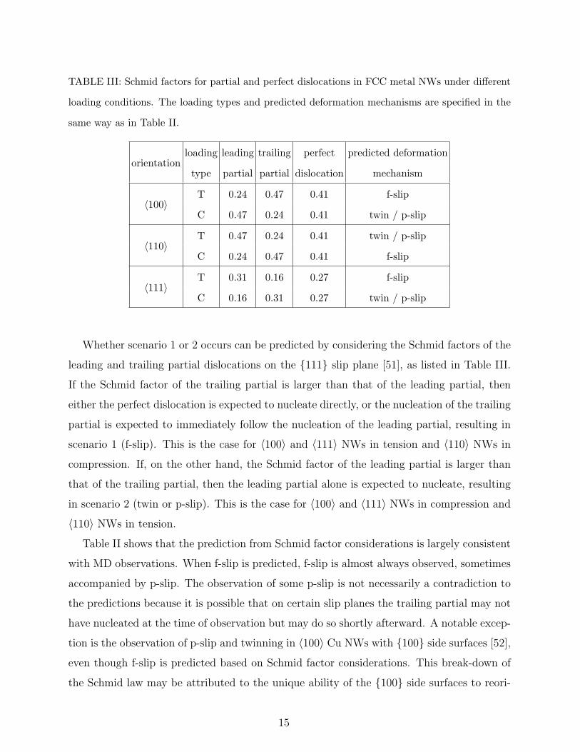
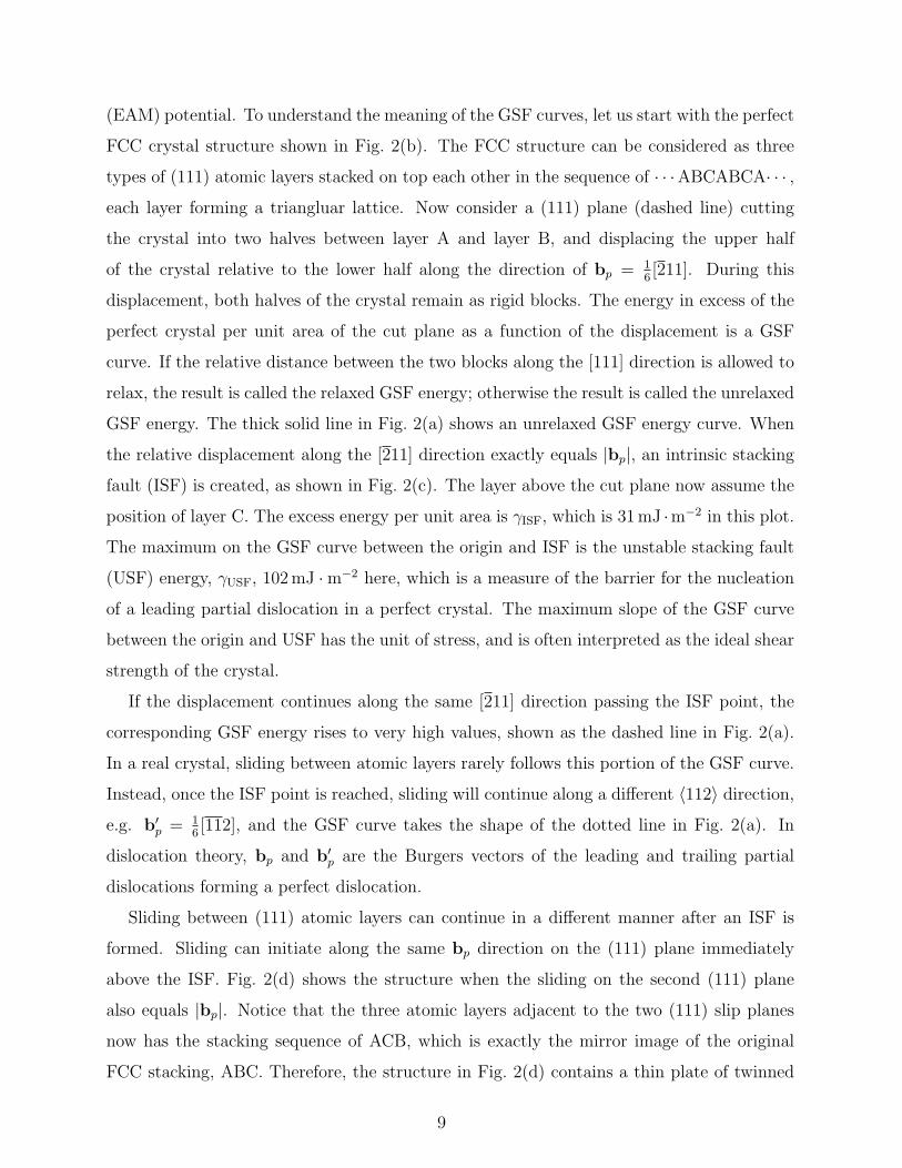
TABLE III: Schmid factors for partial and perfect dislocations in FCC metal NWs under different
loading conditions. The loading types and predicted deformation mechanisms are specified in the
same way as in Table II.
orientationloading leading trailing perfect predicted deformation
type partial partial dislocation mechanism
〈100〉T 0.24 0.47 0.41 f-slip
C 0.47 0.24 0.41 twin / p-slip
〈110〉T 0.47 0.24 0.41 twin / p-slip
C 0.24 0.47 0.41 f-slip
〈111〉T 0.31 0.16 0.27 f-slip
C 0.16 0.31 0.27 twin / p-slip
Whether scenario 1 or 2 occurs can be predicted by considering the Schmid factors of the
leading and trailing partial dislocations on the 111 slip plane [51], as listed in Table III.
If the Schmid factor of the trailing partial is larger than that of the leading partial, then
either the perfect dislocation is expected to nucleate directly, or the nucleation of the trailing
partial is expected to immediately follow the nucleation of the leading partial, resulting in
scenario 1 (f-slip). This is the case for 〈100〉 and 〈111〉 NWs in tension and 〈110〉 NWs in
compression. If, on the other hand, the Schmid factor of the leading partial is larger than
that of the trailing partial, then the leading partial alone is expected to nucleate, resulting
in scenario 2 (twin or p-slip). This is the case for 〈100〉 and 〈111〉 NWs in compression and
〈110〉 NWs in tension.
Table II shows that the prediction from Schmid factor considerations is largely consistent
with MD observations. When f-slip is predicted, f-slip is almost always observed, sometimes
accompanied by p-slip. The observation of some p-slip is not necessarily a contradiction to
the predictions because it is possible that on certain slip planes the trailing partial may not
have nucleated at the time of observation but may do so shortly afterward. A notable excep-
tion is the observation of p-slip and twinning in 〈100〉 Cu NWs with 100 side surfaces [52],
even though f-slip is predicted based on Schmid factor considerations. This break-down of
the Schmid law may be attributed to the unique ability of the 100 side surfaces to reori-
15

ent to the more stable 111 surfaces (see Section III C). Another exception is the case of
〈110〉 NWs with 111 side surfaces under compression, in which deformation proceeds by
atoms piling up around the fixed end of the NWs, instead of through the predicted f-slip
mechanism. This observation may also be attributed to the stability of 111 side surfaces.
When f-slip is not favored from Schmid factor considerations, either twinning or p-slip
is almost always observed. The only exception is 〈110〉 Al NW loaded in tension, where
f-slip is observed even though it is not favored from Schmid factor considerations [46]. This
discrepancy is caused by the high stacking fault energy of Al, and will be removed in the
next subsection when the generalized stacking fault energies are considered.
It is remarkable that the Schmid factor considerations, being purely geometric in nature,
can explain many of the features observed in these MD simulations. However, the Schmid
factor alone does not distinguish twinning versus p-slip, both occurring through the nucle-
ation of the leading partial. From Table II, it appears that p-slip is more favorable for the
〈111〉 NWs (in tension), while twinning is more favorable for the 〈100〉 NWs (in compres-
sion) and the 〈110〉 NWs (in tension). However, it is not clear whether a responsible physical
mechanism can be identified.
B. Effect of generalized stacking fault energy
As noted before, the Schmid factor cannot distinguish between p-slip and twinning.
Therefore, some other criterion is needed to distinguish between the two. MD simula-
tions show that the competition between twinning and p-slip is material dependent. As
shown in Table II, Cu and Ni NWs with 〈110〉 orientation and 111 side surfaces deform
by twinning in tension [46, 57]. However, Au NWs under identical conditions would twin
at low temperatures and slip (by partial dislocations) at higher temperatures and Al NWs
deform by slip via perfect dislocations (f-slip) [46]. To understand this material dependence,
the twinnability parameter derived by Tadmor and Bernstein [48] has been used to rank the
propensity of the materials to twin [46]. The twinnability parameter τa is defined through
the intrinsic stacking fault energy γISF, the unstable stacking fault energy γUSF, and the un-
stable twinning energy γUT. Table I gives the definition of τa and lists its values for Cu, Au,
Ni and Al. The twinnability of these FCC metals can be ranked as, τCua > τNi
a > τAua > τAl
a .
This trend is consistent with the MD observations of 〈110〉 NWs with 111 side surfaces
16

loaded in tension.
While the twinnability parameter provides a qualitative ranking of the FCC metals in
terms of their tendency to twin, the context in which this parameter is derived does not
exactly match the conditions of these NW simulations. First, twinnability was derived
by considering nucleation from a crack tip, but no cracks exist in the NWs at the onset of
plastic deformation. Second, τa is obtained by averaging over all orientations in a polycrystal,
whereas the NWs here are single crystals under uniaxial loading with well defined Schmid
factors. Third, twinnability is designed to distinguish between f-slip and twinning, and is
unable to select from three candidate mechanisms: p-slip, f-slip and twinning.
In the following, we describe a two-parameter criterion based on both the Schmid factor
and the generalized stacking fault energies. Consider the scenario that a leading partial has
already nucleated from the surface of the NW. Three possible events can occur next. First,
another leading partial can nucleate on a parallel plane not adjacent to the first slip plane.
This leads to p-slip, and the critical (axial) stress can be estimated from the maximum
slope of the GSF curve from origin to USF, i.e., σcp = α γUSF/(bpSlead), where α ≈ π is a
geometric factor, bp is the magnitude of the partial Burgers vector, and Slead is the Schmid
factor of the leading partial. Second, the trailing partial can nucleate on the same slip plane
of the leading partial. This leads to f-slip, and the critical stress can be estimated from
the maximum slope of the GSF curve between ISF and USF (dotted line in Fig. 2(a)), i.e.,
σcf = α (γUSF−γISF)/(bpStrail), where Strail is the Schmid factor of the trailing partial. Third,
a leading partial can nucleate on the slip plane adjacent to the first leading partial. This
leads to twinning, and its critical stress can be estimated as, σct = α (γUT − γISF)/(bpSlead).
In this model, the event with the lowest critical stress is predicted to occur. The situation
can be visualized in a map spanned by two parameters,
τ1 ≡σc
p
σct
=γUSF
γUT − γISF
(3)
τ2 ≡σc
f
σct
=γUSF − γISF
γUT − γISF
· Slead
Strail
(4)
As shown in Fig. 5, the parameter space can be divided into three domains, corresponding
to p-slip, f-slip and twin, respectively, depending on the relative magnitude of τ1, τ2 and 1.
To a very good approximation, Slead/Strail only takes two possible values for all six loading
conditions listed in Table III, i.e. Slead/Strail ≈ 0.51 for 〈100〉 T, 〈110〉 C, 〈111〉 C, and
Slead/Strail ≈ 1.95 for 〈100〉 C, 〈110〉 T, 〈111〉 T. Therefore, each point in Fig. 5 represents
17

0 1 20
1
2
CuNi
Au
Alf−slip
p−slip twin
CuNi
AuAl
τ1
τ 2
FIG. 5: Deformation mechanism map of FCC metal NWs under different axial loading conditions.
The p-slip domain: τ1 < τ2 and τ1 < 1. The f-slip domain: τ2 < τ1 and τ2 < 1. The twin
domain: τ1 > 1 and τ2 > 1. Open symbols correspond to the loading conditions of 〈100〉 tension,
〈110〉 compression, 〈111〉 compression. Filled symbols correspond to the loading condition of 〈100〉
compression, 〈110〉 tension, 〈111〉 tension.
one NW material and three loading conditions.
Fig. 5 shows that under 〈100〉 T, 〈110〉 C, and 〈111〉 C loading conditions, all four metals
fall within the domain of f-slip, consistent with MD observations and the predictions based
on Schmid factor alone. Under 〈100〉 C, 〈110〉 T, and 〈111〉 T loading conditions, Al falls
within the domain of f-slip, consistent with MD observations [46], while Cu, Ni, Au all fall
in the domain of twinning. These predictions are also listed in Table II.
The present model predicts that, as long as f-slip is not the dominant mechanism, twin-
ning is always favored over p-slip. This is not entirely consistent with MD simulations,
summarized in Table II, in which p-slip are observed under certain conditions. However,
both p-slip and twinning occur through the stochastic event of dislocation nucleation, so
that the boundary between the two mechanisms is not abrupt. In addition, if one accounts
for the finite temperate and high strain rate in MD simulations, the boundary between p-
slip and twin should shift to the right. This is because the nucleation rate of p-slip will be
enhanced by the availability of multiple nucleation sites on the NW surface. We note that
in Fig. 5, the points for Au, Cu and Ni lie close to the boundary between p-slip and twin.
Au lies closest to the boundary, which is consistent with the greater tendency of Au toward
p-slip as observed in MD simulations.
18

C. Effect of side surfaces
Table II shows that the competition between p-slip and twinning is influenced by the side
surfaces of 〈100〉 and 〈110〉 oriented NWs. Neither the Schmid factor nor the generalized
stacking fault energies, as discussed in the above two subsections, can account for the effect
of side surfaces on deformation mechanisms. The effect of the side surface orientation
can be accounted for, in principle, by considering surface step energies. The nucleation of
an isolated partial dislocation from NWs with smooth surfaces will lead to a surface step,
and the step energy increases the free energy barrier for p-slip nucleation. The nucleation
of another partial dislocation on the slip plane immediately above that of the first partial
(i.e. forming a micro-twin) may incur a lower step energy cost, if it effectively reorients the
side surface to a lower energy facet. This explains why 〈100〉 NWs with 100 side surface
deform by twinning in compression (because they reorient to 111 after twinning), while
those with 110 and 001 surfaces deform by p-slip.
An aspect that has been ignored in the above discussions and MD simulations is that even
high quality as-fabricated NWs have some surface roughness. Surface roughness produces
local stress concentrations which promote dislocation nucleation around a small region.
This favors twinning, which requires sequential nucleation of leading partials on adjacent
slip planes. Therefore, even if p-slip is predicted by MD simulations, we would expect to
find thin twin lamella in experiments, with the thickness of the lamellae determined by
the roughness of the side surface. In the experiment by Zheng et al. [18], the dominant
deformation mechanism in 〈100〉 Au nanocrystals loaded in tension is f-slip, consistent with
Table II. However, limited twinning also occurs in the same loading condition, which is
probably caused by the local surface roughness.
It is worth noting that some MD simulations predict that 〈110〉 Au NWs deform in
tension by twinning at very low temperatures but transition to p-slip at temperatures above
200 K [46]. One explanation is that the relative influence of the step energy reduces with
temperature as the size of the critical dislocation nucleus increases. The explicit temperature
dependence of GSF energies [58] can also lead to a temperature induced transition from
twinning to slip. However, Zheng et al. [18] observe that 〈110〉 Au NWs loaded in tension
deform by twinning at room temperature. This is in agreement with the two-parameter
model shown in Fig. 5, as well as MD predictions from other groups [51, 57].
19

Occasionally, the effect of side surfaces can override the predictions based on the Schmid
factor, as in the case of Cu 〈100〉 with 100 side surfaces in tension [52]. The preference to
twinning over f-slip (as predicted by the Schmid factor) has been attributed to the ability of
100 surface to orient to 111 surface. Nonetheless, it is still surprising that the trailing
partial has not been observed for Cu NWs of this geometry [52, 54], even though its Schmid
factor is twice of the Schmid factor of the leading partial. This may be caused by the
shape of the NW cross section. According to [59], dislocation prefers to nucleate at the NW
corner, but has an even stronger preference to be close to the screw orientation (i.e. parallel
to the Burgers vector). Therefore, a preferred corner for leading partial nucleation may be
an unfavorable site for trailing partial nucleation. More study is needed to understand why
the trailing partial fails to nucleate in these NWs.
IV. YIELD STRENGTH
During the last 7 years, there has been significant interest in the compression (and more
recently, tension) tests of micro-pillars fabricated using the focused ion beam (FIB) [21].
These experiments have shown that the flow stresses of single crystal micro-pillars increase
dramatically as their diameters decrease from 10 µm to 100 nm. This naturally raises the
question: how does the yield strength depend on diameter for nano-pillars or nanowires with
diameters less than 100 nm? While the experimental data for NWs is starting to emerge
[17, 18, 60, 61], computer simulations have been applied extensively to predict the strength
of NWs. In this section, we review the current understanding of the strength of metal NWs
based on computer simulations and theoretical models.
Fig. 6(a) shows representative stress-strain curves of FCC NWs of different orientations
under uniaxial tension or compression predicted by MD simulations. At small enough strains,
the NW remains elastic, i.e. the stress-strain curve is completely reversible. The stress-
strain curve is a smooth (potentially non-linear) function in the elastic regime. Beyond a
critical strain, the stress drops abruptly and the stress-strain curve becomes irreversible upon
unloading. The stress at this critical condition is called the yield stress (or yield strength)
σY .
MD simulations have predicted that the yield stress of FCC metal NWs depends on the
orientation and size of the NWs, the type of loading (tension versus compression), strain rate,
20

FIG. 6: (a) Uniaxial tensile and compressive stress-strain curves for FCC Au NWs oriented along
〈111〉 and 〈100〉 orientations with square (4 nm×4 nm) cross section. (b) The yield stress of 〈100〉
and 〈111〉 Au NWs with square cross sections as a function of their size. (Reprinted with permission
from [62].)
and temperature. However, in bulk FCC metals, the yield stress is approximately symmetric,
weakly strain rate dependent and the yield stress divided by the Young’s modulus is nearly
independent of temperature [63]. The following is a summary of the observations from MD
simulations on the yield stress of FCC metal NWs.
• The yield stress depends on NW orientation and whether the NW is loaded in tension
or compression (see Fig. 6(b)). For example, the magnitudes of the yield strength for
a 6 nm thick Au 〈100〉 NW in tension and compression are different by more than a
factor of 4. The three most studied orientations are 〈100〉, 〈110〉, and 〈111〉 [55, 62].
• The yield stress varies with NW width d. A behavior of the form of σY = σ∞Y +K d−1
is often observed, where σ∞Y and K are independent of d [56, 62].
• The yield stress strongly depends on the shape of the NW cross section. For example,
the yield stress at 300 K of Cu 〈111〉 NWs is about 10 GPa for circular cross sections
but only about 6.5 GPa for square cross sections [53].
• The yield stress decreases with increasing temperature [44, 53, 55]. The temperature
dependence has been observed to follow two trends: σY = σ0 − AT and σY = σ0 −
A√T depending on the interatomic potential model. The strength reduction with
temperature can be as much as 50% from 0 K to 500 K.
21

There is a general consensus that FCC NWs (both in experiments and MD simulations)
should be free of dislocations before loading, such that yielding is controlled by disloca-
tion nucleation from the surface. In other words, the NWs are in a “dislocation-starved”
state [30]. Therefore, the dependence of yield strength on geometry, loading type, strain
rate, and temperature should be understood in terms of the critical condition for dislocation
nucleation. In the following, the behavior of yield strength is rationalized in terms of Schmid
factor, surface stress, and nucleation rate theories. Alternative nucleation or yield criteria
that have been proposed in the literature are discussed afterwards. However, the only theory
that can explain all of the MD observations that are potentially relevant at experimental
strain rates is classical nucleation theory.
A. Effect of Schmid factor and surface stress
The first nucleation event upon yielding, in all existing MD simulations, is the nucle-
ation of the leading partial. This event is the rate limiting step that determines the yield
strength [53, 62]. Hence, the variation of the Schmid factor of the leading partial with NW
orientation and loading type, as listed in Table III, naturally contributes to the dependence
of the yield strength on these two parameters. This suggests that the critical resolved shear
stress (CRSS), which is the yield stress multiplied by the Schmid factor of the leading partial,
may be a better criterion for yielding than the normal stress along the NW axis.
As discussed in Section II, the surface stress induces a compressive stress at the interior
of the NW in the absence of the applied load. As a result, the stress at the interior of
the NW is different from the applied stress. Taking into account the effects from both the
Schmid factor and the surface stress, Fig. 7 plots the CRSS at the interior of the NW at the
onset of yielding [53]. The dependence on NW width is now almost completely removed,
showing that the surface stress is the dominant cause of the size dependence. The tension-
compression asymmetry in Fig. 7 is also significantly reduced compared with Fig. 6(b). This
shows that the Schmid factor of the leading partial and the surface stress are the primary
causes of the tension-compression asymmetry.
While the Schmid factor and surface stress explanations have proved to be very useful,
certain observations in the MD simulations still remain puzzling. First, it is not clear why
the yield strength of Au 〈100〉 NWs in tension have a much weaker size dependence than
22

FIG. 7: The resolved shear stress on the interior of a Au NW at yielding. (Reprinted with
permission from [62].)
in compression (see Fig. 6(b)) [62]. Second, there still exists an un-explained orientation
dependence and tension-compression asymmetry, as shown in Fig. 7, even after both the
Schmid factor and surface stress effects have been factored out. These behaviors may be
caused by rearrangement and energetics of the surface atoms during dislocation nucleation.
B. Classical nucleation theory
Classical nucleation theory (CNT) [64–69] provides an appropriate framework to discuss
the dislocation nucleation rate and hence the yield strength of NWs. According to CNT,
the dislocation nucleation rate under stress σ and temperature T is given by the following
expression,
I(σ, T ) = Ns ν0 exp
[−Gc(σ, T )
kBT
](5)
where Ns is the number of equivalent nucleation sites, ν0 is a frequency prefactor, Gc is
the activation Gibbs free energy for dislocation nucleation, and kB is Boltzmann’s constant.
The Becker-Doring theory [64] gives an explicit expression for ν0, which can be computed
by atomistic simulations [68, 69]. ν0 is often approximated by the Debye frequency νD of
the crystal, which is typically on the order of 1013 s−1.
Roughly speaking, the yield strength σY of the NW is the stress at which the dislocation
nucleation rate reaches a threshold value, i.e. I(σY , T ) = Ith. The threshold nucleation rate,
Ith, is the inverse of the characteristic time in which the NW is subjected to stress σY . For
constant strain rate experiments and simulations, Ith is on the order of the strain rate, which
23

is about 108 s−1 for MD simulations and 10−3 s−1 for experiments.
Eq. (5) shows that the nucleation rate is very sensitive to the activation Gibbs free energy
Gc(σ, T ). For a given T , Gc(σ, T ) usually decreases rapidly with σ, so that the nucleation
rate I(σ, T ) is very sensitive function to stress. The activation volume, defined as:
Ω(σ, T ) ≡ −∂Gc(σ, T )
∂ σ
∣∣∣∣T
(6)
measures the sensitivity of Gc(σ, T ) to the applied stress σ and is approximately the mag-
nitude of the Burgers vector times the area enclosed by the critical dislocation loop for
dislocation nucleation [69].
The following implicit equation for the yield strength σY has been derived [67, 70] by
considering a scenario in which the NW is loaded at a constant strain rate ε.
Gc(σY , T )
kBT= ln
kB T Ns ν0
E εΩ(σY , T )(7)
This equation is derived based on the assumption that the NW remains linear elastic with
Young’s modulus E prior to yielding and that ν0 is insensitive to σ and T . These are
reasonable assumptions for the experimental conditions, although the NWs usually become
non-linear elastic prior to yielding in many MD simulations.
By numerically solving Eq. (7), we can predict the yield strength σY , provided with
the knowledge of the activation Gibbs free energy Gc(σ, T ) and reasonable estimates of Ns
and ν0. Gc(σ, T = 0) can be determined from zero temperature chain-of-states methods,
such as the nudged elastic band [71] and string [72] methods, directly applied to atomistic
models. Alternatively, continuum models can be used, but the accuracy of these models are
limited by the approximation introduced at the dislocation core. Finally, the temperature
dependence of Gc(σ, T ) has been approximated using the thermodynamic compensation law
(or Meyer-Neldel Rule) [67], as well as determined numerically by umbrella sampling [68, 69].
The yield stress predicted by Eq. (7) has several generic features that are in agreement
with the observations from MD simulations. These agreements support the point of view
that the yield strength of NWs can be understood by properly applying classical nucleation
theory to dislocation nucleation from the NW surface.
The first evidence from MD simulations in support of CNT is the dramatic decrease of
yield strength as the NW cross section changes from a circle to a square [53, 59]. The
dislocation nucleus in a square pillar will have, in general, a shorter line length than in
24

circular pillars leading to a lower Gc and σY [59]. Additionally, square cross-sections may
induce a stress concentration due to the surface stress [53] which further enhances nucleation
from the corners.
Another piece of strong evidence in support of CNT is the reduction of yield strength
with increasing temperature [53, 55]. This is a consequence of the thermally activated
nature of the dislocation nucleation process and is naturally obtained when Eq. (7) is solved
numerically. The strong temperature dependence of the yield strength is consistent with a
relatively small activation volume (compared with, e.g. forest cutting mechanisms in the
bulk [73]) of the dislocation nucleation process under the high stress conditions of these MD
simulations.
The CNT approach also makes other interesting predictions concerning the yield strength
of NWs under experimental conditions. First, the yield strength is predicted to depend on
the applied strain rate ε, which is explicitly included in Eq. (7). The reduction of strain rate
from MD values, on the order of 108 s−1, to experimental values, on the order of 10−3 s−1,
can lower the yield strength by several hundred MPa’s [67, 68]. This allows extrapolation
of MD results to predict NW yield strength at experimental conditions.
Second, Eq. (7) predicts a dependence of NW yield strength on NW size, through the
number of nucleation sites Ns. A thicker (or longer) NW has more nucleation sites than
a thinner (or shorter) NW and will have a somewhat lower yield strength. However, this
effect only leads to a logarithmic dependence of σY on the NW width d, and is much weaker
than the 1/d dependence arising from the surface stress effect (Section IV A). Hence, the
dominant mechanism for the size effect of yield strength for FCC metal NWs is the surface
stress.
C. Alternative nucleation criteria
In the previous subsection, we presented the view point that the yield strength of NWs
can be understood through classical nucleation theory, in terms of the activation free energy
Gc for dislocation nucleation as a function of the applied stress σ and temperature T .
However, there have been several reports suggesting the need for an alternative approach.
For example, Zepeda-Ruiz et al. [56] proposed that the local stress in the surface layer instead
of the applied stress should be used as a yield criterion. Cao and Ma [53] proposed the local
25

shear strain on surface atoms as a yield criterion. Park and Zimmerman [44] suggested that
the strengthening is caused by changes in dislocation drag. Both Rabkin et al. [55] and
Marian and Knapp [74] have suggested buckling as an important event prior to dislocation
nucleation. Rabkin et al. [55] have also proposed a strain based nucleation criterion that
accounts for the temperature induced strain fluctuation. In this section, we discuss these
approaches and show that they are either consistent with the CNT based approach, or are
unlikely to influence the NW yield strength at the experimental strain rates.
In their study of Au 〈100〉 NWs under compression, Zepeda-Ruiz et al. [56] claim that the
applied stress σ is not the controlling factor for dislocation nucleation, because, interestingly,
the applied stress actually drops (at low temperatures) prior to dislocation nucleation. To
explain their observations, the authors propose that the local stress in the surface layer
atoms (terraces) should be used as the nucleation criteria. The authors note that during
compression the 110 terraces experience higher stresses than the 100 terraces, and
this fact correlates with the observation of preferred nucleation sites on the 110 terraces.
However, unlike the Virial stress which is well defined as the average stress over the entire
simulation cell, there is no unique definition for the local stress of a small group of atoms [75].
It is not clear whether the rapid increase of the local (compressive) stress on 110 facets
prior to yielding is a consequence of the specific choice of local stress definition used in the
analysis. In addition, while the above observation is important for understanding how the
NWs yield in MD simulations, it is likely that at the experimental strain rate the NWs will
nucleate dislocations under much lower stresses, up to which the NWs are still linear elastic.
To analyze their MD simulations of Cu NWs, Cao and Ma [53] introduced the notion of
local strain shear invariant (SSI), which measures the amount of shear deformation around
each atom. They observe that in both NWs with square cross sections and NWs with circular
cross sections, dislocation nucleation occurs when certain atoms have their SSI exceeding a
threshold value of 0.085. Despite this correlation, it is not clear how the SSI parameter can
explain temperature or strain rate dependence of the yield strength. As mentioned above,
at experimental time scales, metal NWs are likely to remain linear elastic prior to yielding
such that the resolved shear strain (proposed in [53]) and resolved shear stress (used in [62])
are proportional to each other.
Park and Zimmerman [44] suggested that phonon drag has an effect on the strength of
NWs and explains the strain rate dependence of yield strain. While phonon drag has been
26

shown to be size dependent below 40 nm [76], it is unlikely to be important in nucleation
since phonon drag only relates to the motion of the dislocations after they are nucleated.
The change in yield strength with strain rate observed in these MD simulations can be fully
explained by CNT through Eq. (7), and the size dependence can be explained through the
surface stress.
In their simulations of Au NWs in compression, Rabkin et al. [55] observed a number of
cases in which dislocation nucleation is preceded by a buckling instability of the NW. This
behavior is observed in 〈100〉 and 〈110〉 NWs when certain interatomic potentials are used
but not in 〈111〉 NWs. However, it is reasonable to expect that at experimental time scales
dislocation nucleation will occur at much lower stresses and will not be driven by elastic
buckling (for nanopillars of the aspect ratio in [55]). The same argument applies to the
surface wrinkling observed by Marian and Knap [74] in the compression simulations of Au
〈100〉 nano-pillars using the quasi-continuum method.
In the cases where dislocation nucleation is not preceded by an elastic instability (e.g.
for 〈111〉 NWs), Rabkin et al. [55] proposed a strain-based dislocation nucleation criterion
to explain the temperature dependence of the yield strength, in the spirit of the Lindemann
criterion for melting [77]. First, the authors defined a “thermal strain”, εtherm ≡ 〈∆r〉/a,
where 〈∆r〉 is the average distance of an atom from its equilibrium position, and a is the
equilibrium lattice constant. Second, the authors found that, under zero applied stress,
εtherm increases with T for both surface and bulk atoms, in the form of either A√T or AT ,
depending on the interatomic potential. Third, the temperature dependence of the NW
yield stress (when yield is not controlled by elastic buckling) can be well described by the
empirical relation,
σY (T ) = E(T ) [ εc − εtherm(T ) ] (8)
where E is the Young’s modulus and εc is an empirical constant. While Eq. (8) seems
to agree well with their MD observations, it is not clear how this heuristic relationship
can be explained except through classical nucleation theory, which not only captures the
temperature dependence, but also geometric and strain rate effects.
27
V. PHASE TRANSFORMATION
In addition to slip and twinning, both of which are controlled by the nucleation of lattice
dislocations, phase transformations between the FCC and the BCT (body-centered tetrag-
onal) have been predicted as an alternative plastic deformation mechanism for very thin
〈100〉 FCC metal NWs [78–80]. In the existing studies, the FCC-BCT phase transformation
occurs spontaneously under zero applied load, leading to contraction of the NW length, and
is entirely driven by the surface stress. Intermetallic Ni-Al [81] and Cu-Zr [82] NWs with
initial B2 phase have been shown to undergo reversible transformations between the B2 and
BCT phases during tensile loading and unloading, which leads to a pseudo-elastic behavior
to be discussed in the next section.
FCC BCC
FIG. 8: Bain path transforming FCC structure to BCC structure.
To understand the FCC-BCT phase transformation, one must first consider the Bain
path [83, 84]. Along the Bain path, a bulk FCC crystal can homogeneously transform into
a BCC (body-centered cubic) structure. This is achieved by contracting along the [100]
direction and simultaneously expanding along the [010] and [001] directions of the FCC
structure. When the length along the [100] direction becomes a factor of√
2 of the lengths
along the [010] and [001] directions, the distorted FCC structure becomes a BCC structure,
as shown in Fig. 8. The [010] and [001] directions of the BCC structure corresponds to
the [011] and [011] directions of the original FCC structure. However, if the transformation
along the Bain path does not stop at the exact proportion given above, the result is a BCT
structure. BCT is a distorted BCC structure, i.e. the length along the new [100] direction
is not the same as those along the new [010] and [001] directions.
28

The FCC-BCT transformation does not occur homogeneously over the entire NW. In-
stead, the transformation is initiated at the two ends and proceeds by propagating the two
(100) phase boundaries towards each other along the NW axis [78]. Therefore, the FCC-BCT
phase transformation also occurs in a layer-by-layer fashion, as in twinning. The B2-BCT
phase transformation predicted for Cu-Zr NWs [82] also proceeds by the propagation of
(100) phase boundaries, which are normal to the NW axis. However, the B2-BCT phase
transformation predicted for Ni-Al NWs [81] proceeds by the propagation of 101 phase
boundaries, which are inclined to the NW axis, making the transformation mechanism more
similar to twinning discussed in previous sections.
MD simulations using the Au MEAM potential predict that the FCC-BCT phase trans-
formation only occurs in a narrow range of NW diameters [38, 78]. Au 〈100〉 NWs with
cross section area larger than 4 nm2 relaxes by reorientation into FCC 〈110〉 NWs through
twinning, as discussed earlier. In contrast, all Au EAM potentials predict 〈100〉-to-〈110〉
reorientation instead of FCC-BCT phase transformation for all NW diameters. Ab-initio
methods (DFT and TB) have been used to study the FCC-BCT phase transformation as
well [79, 80]. The result show that all BCT phases are unstable in the bulk, however, the sur-
face stresses in NWs can stabilize the Au and Pt BCT phases. Nonetheless, the BCT 〈100〉
NW structure is always higher in energy than the reoriented FCC 〈110〉 NW. Therefore, at
the experimental time scales, the BCT NW may be very short-lived before it spontaneously
transforms to the reoriented FCC structure. In this case, the BCT structure acts as an
intermediate step for the 〈100〉-to-〈110〉 reorientation transformation, as observed in some
simulations [80].
Recently, Zheng et al. [18] have shown that some nanocrystals appear to change phase or
reorient after fracture. The authors believe that the final phase is BCT Au. However, the
evidence is not conclusive since the imaging is based on a single two-dimensional image. It
is reasonable to expect phase transformation to be a viable deformation mechanism in other
types of metal NWs, such as intermetallic NWs [81, 82].
VI. PSEUDO-ELASTIC AND SHAPE MEMORY EFFECTS
Pseudo-elastic and shape memory effects are two closely related phenomenon in which
materials deform reversibly to very high (e.g. 10%) strains. In the pseudo-elastic effect, the
29

sample recovers its original shape as soon as the load is removed. In the shape memory
effect, heating is required for shape recovery after the load is removed. This surprising
behavior can appear when deformation is caused by moving interfaces between different
crystalline phases or twins [85–88]. In bulk samples, the pseudo-elastic and shape-memory
effects have been found in alloys (e.g. Cu-Zn, Ni-Ti), but not in single-component metals.
However, both the pseudo-elastic and shape-memory effects have been predicted to occur in
single-component FCC metal NWs due to the strong surface stress effects at the nanoscale.
MD simulations have shown that, under compression, FCC 〈100〉 NWs with 100 side
surfaces transform into 〈110〉 NWs with 111 side surfaces by twinning [38, 46, 57, 89, 90].
Under tension, the reverse transformation occurs also by the same twinning mechanism.
This transformation between the two FCC NW structures has been called reorientation.
When the NW is sufficiently thin, the surface stress alone can induce reorientation from the
〈100〉 direction to the 〈110〉 direction in the absence of an applied load [46, 57, 89, 90]. The
resulting 〈110〉 NW can transform to the 〈100〉 orientation when a sufficiently large tensile
load is applied. As soon as the load is removed, however, the surface stress spontaneously
transforms the NWs back to the 〈110〉 orientation. The maximum reversible strain of this
reversible transformation can be estimated as√
2 − 1 = 41.4%, leading to a very large
pseudo-elastic effect.
For slightly thicker FCC 〈100〉 NWs, the surface stress alone is not sufficient to initiate
twinning and cause reorientation at room temperature, but this reorientation can occur at
elevated temperatures. In this case, after the FCC 〈110〉 NW reorients to the 〈100〉 direction
under tension, the structure remains meta-stable even after the load is removed. The NW
returns to the 〈110〉 orientation when it is heated to a higher temperature, leading to a
shape memory effect. The existence of a critical temperature to initiate the 〈100〉-to-〈110〉
reorientation is caused by the presence of a free energy barrier for the first partial dislocation
to nucleate from the NW surface. After the first nucleation event, the nucleation barriers
of subsequent partial dislocations on adjacent 111 planes are apparently lower, resulting
in continued propagation of the twin and thus reorientation of the NW. The 〈110〉 oriented
NW is always in a lower energy state than the 〈100〉 oriented NW because the 〈110〉 oriented
NW has a smaller total surface area as well as a lower surface energy per unit area. Hence it
is reasonable to expect the 〈100〉-to-〈110〉 reorientation to occur given sufficient assistance
from thermal fluctuation.
30

The ability of FCC NWs to exhibit shape memory and psuedo-elastic effects depends
on both the material as well as the interatomic potentials models. For example, using
EAM potentials, Liang and Zhu predict [46] that Cu exhibits both pseudo-elastic and shape
memory effects, Ni shows pseudo-elastic effects, Au exhibits pseudo-elastic effect at very
low temperatures, and Al does not show either pseudo-elastic or shape memory effect at all.
Park et al. [57] showed that Cu, Ni and Au NWs all show both pseudo-elastic and shape
memory effects with different critical temperatures. The different predictions for Ni are
most likely caused by the difference in the interatomic potentials, causing different surface
stresses and energy barriers to dislocation nucleation.
The tendency for NWs to exhibit pseudo-elastic and shape memory effects is controlled
by the competition between twinning and slip, which is discussed in Section III. Al has the
lowest twinnability of the material studied and 〈110〉 NWs fail via f-slip (see Fig. 5) and
thus exhibit no pseudo-elastic or shape memory effects. Au has the next lowest twinnability
and pseudo-elastic only at low temperatures. Cu and Ni show show transitions between
pseudo-elastic and shape memory effects that are size and temperature dependent.
MD simulations [78–80] using the MEAM potential have predicted that Au 〈100〉 NWs
can spontaneously undergo FCC-BCT phase transformation driven by the surface stress
(see Section V). If the BCT phase can transform back to the FCC 〈100〉 NW structure
under tension, then the result is a pseudo-elastic or shape memory effect, via the phase
transformation instead of the reorientation mechanism. However, this possibility has not
yet been investigated by MD simulations. A similar mechanism, the B2-BCT phase trans-
formation, has indeed been found to lead to the pseudo-elastic and shape memory effects
for intermetallic Ni-Al [81] and Cu-Zr [82] NWs.
The possibility of pseudo-elastic and shape memory effects for FCC NWs has not been
studied for 〈100〉 NWs with cylindrical side surfaces, even though these NWs have been
predicted to twin and reorient to the 〈110〉 direction under compression [55]. This possibility
seems likely given that reoriented 〈110〉 NWs should have a lower energy than 〈100〉 NWs.
Recent experiments have validated the predicted reorientation in Au NWs with diameters
of 40-150 µm [60]. The NWs are initially along 〈110〉 direction with atomically smooth 111
side surfaces and rhombic cross sections. Twins are nucleated at 1.5 GPa axial stress, and
propagate through the NWs to reorient them. The reoriented NWs are along 〈100〉 direction
with 100 side surfaces and rectangular cross sections. This remarkable validation suggests
31

that MD simulations, even though limited to high strain rate conditions, have the potential
to be predictive for deformation mechanisms at the experimental strain rate.
VII. BENDING AND TORSION
The previous four sections have primarily dealt with plasticity of FCC NWs under uniaxial
loading. Given the complexity of deformation behavior already observed in MD simulations
and the difficulty of conducting nanoscale experiments, it is understandable that so much
attention has been focused on the simple uniaxial loading condition. In this section, we
discuss some of the simulations [91–96] of the bending and torsion of metal NWs. One of the
unique opportunities in studying NWs in bending and torsion is that these loading conditions
provide the opportunity to study the effects of strain gradients on NW plasticity. Strain
gradients imposed by the loading condition lead to geometrically necessary dislocations
(GND) that accommodate a plastic twist or curvature [97]. Due to GND’s, NWs are no
longer dislocation starved, leading to a different realm of plastic behaviors.
A. Bending
Zheng et al. [91, 92] have conducted MD simulations of the bending of 〈100〉 oriented
Cu NWs. The NWs have square cross section and are initially defect free. The plastic
deformation is dominated by p-slip and twinning, not unlike the deformation of Cu NWs
under uniaxial loading. Furthermore, plasticity is always initiated from the compressive side
of the 〈100〉 NW. This is consistent with fact that the leading partial has a higher Schmid
factor when a 〈100〉 NW is in compression than in tension, as listed in Table III. At a later
stage of deformation, fivefold deformation twin structures are commonly observed in these
bending simulations.
In a related study, Csikor et al. [93] have used a continuum model of the statistics of
dislocation avalanches to predict that deformation in bent wires transitions from diffuse to
localized as the wire diameter reduces from millimeters to a micron. This suggests that in
bent NWs, the plastic deformation should be completely localized. However, the statistical
nature of dislocation avalanches is not necessarily the same as that of dislocation nucleation,
which controls NW plasticity. Because NW orientation plays a significant role in dislocation
32

nucleation under uniaxial loading, it would be interesting to see if and how NW plasticity
in bending depends on NW orientation from atomistic simulations.
B. Torsion
The torsion of Au and Al NWs has been studied using both MD and dislocation dy-
namics [94–96]. The authors investigate the size and orientation dependent plasticity which
included three high symmetry orientations: the 〈100〉, 〈110〉 and 〈111〉. For 〈111〉 and 〈100〉
orientations, low angle twist boundaries are observed to form on the (111) and (100) planes
perpendicular to the wire axis by the nucleation and organization of perfect dislocations
on their 111 slip planes as shown in Fig. 9(a)-(b). Continued plasticity occurs at this
boundary as it evolves into a high angle grain boundary localizing the plastic deformation.
The 〈110〉 NWs accommodate the plastic twist in a very different way from 〈111〉 and
〈100〉 NWs. The dislocations that nucleate are parallel to the NW axis on 111 slip planes
that are also parallel to the axis. Fig. 9 (c) shows that the first few nucleation events in Au
NWs give rise to the leading partial dislocations with Burgers vectors of the a6〈112〉 type.
For Au NWs below 15 nm in diameter, these are the only types of dislocations observed.
However, in Al NWs of all diameters and some Au NWs, the trailing partial dislocation
quickly follows and the NW is filled with perfect screw dislocations. An example of perfect
dislocations in Al NWs is shown in Fig. 9 (d).
A screw dislocation lying along the axis of a wire was originally studied by Eshelby [98]
in which he considered the screw dislocation as a grown-in defect in whiskers. The twist
caused by such a dislocation is now termed the Eshlby twist. The MD simulations discussed
above predict that the Eshelby twist involving screw dislocations along the wire axis can be
a deformation mechanism for metallic NWs or whiskers.
C. Pseudo-elasticity of 〈110〉 NWs
The unique deformation mechanisms of 〈110〉 NWs in torsion gives rise to a pseudo-
elastic effect and potentially a shape memory effect [94, 95]. As noted above, when FCC
〈110〉 NWs are subjected to torsion, dislocations parallel to the NW axis are nucleated. For
Au NWs of 15 nm diameter and below, only leading partials are nucleated, while Al NWs
33

(a) Au [111] (b) Au [100]
(c) Au [110] (d) Al [110]
FIG. 9: Dislocation structure of FCC metal (Au and Al) NWs of different orientations subjected
to torsion. ( Reprinted with permission from [94] and [95].)
always nucleate perfect dislocations. This mechanistic difference leads to different types of
torque-twist curves for 5 nm diameter Au and Al NWs. When a Au NW is unloaded, the
twist angle returns to zero when the applied torque drops to zero, exhibiting a pseudo-elastic
behavior, as defined in Section VI. This is because the partial dislocations parallel to the
NW axis are unstable in the absence of applied torque. They are pulled out of the NW by
the stacking faults. In comparison, when the Al NW is unloaded, a non-zero twist angle
persists even when the applied torque drops to zero, which signifies irreversible plasticity.
Continuum analysis confirms that multiple perfect screw dislocations are meta-stable inside
an elastic cylinder [95, 96], as in the case of Al NWs. However, a NW containing screw
dislocations parallel to its axis has a higher energy than a defect-free NW. Hence it is
possible that these screw dislocations can leave the NW at an elevated temperature, giving
rise to a shape-memory effect. This possibility has not yet been studied by MD simulations
or experiments.
34
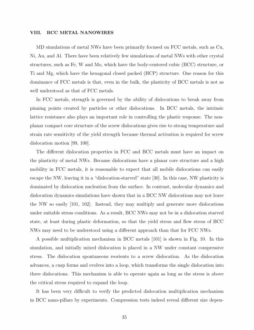
VIII. BCC METAL NANOWIRES
MD simulations of metal NWs have been primarily focused on FCC metals, such as Cu,
Ni, Au, and Al. There have been relatively few simulations of metal NWs with other crystal
structures, such as Fe, W and Mo, which have the body-centered cubic (BCC) structure, or
Ti and Mg, which have the hexagonal closed packed (HCP) structure. One reason for this
dominance of FCC metals is that, even in the bulk, the plasticity of BCC metals is not as
well understood as that of FCC metals.
In FCC metals, strength is governed by the ability of dislocations to break away from
pinning points created by particles or other dislocations. In BCC metals, the intrinsic
lattice resistance also plays an important role in controlling the plastic response. The non-
planar compact core structure of the screw dislocations gives rise to strong temperature and
strain rate sensitivity of the yield strength because thermal activation is required for screw
dislocation motion [99, 100].
The different dislocation properties in FCC and BCC metals must have an impact on
the plasticity of metal NWs. Because dislocations have a planar core structure and a high
mobility in FCC metals, it is reasonable to expect that all mobile dislocations can easily
escape the NW, leaving it in a “dislocation-starved” state [30]. In this case, NW plasticity is
dominated by dislocation nucleation from the surface. In contrast, molecular dynamics and
dislocation dynamics simulations have shown that in a BCC NW dislocations may not leave
the NW so easily [101, 102]. Instead, they may multiply and generate more dislocations
under suitable stress conditions. As a result, BCC NWs may not be in a dislocation starved
state, at least during plastic deformation, so that the yield stress and flow stress of BCC
NWs may need to be understood using a different approach than that for FCC NWs.
A possible multiplication mechanism in BCC metals [101] is shown in Fig. 10. In this
simulation, and initially mixed dislocation is placed in a NW under constant compressive
stress. The dislocation spontaneous reorients to a screw dislocation. As the dislocation
advances, a cusp forms and evolves into a loop, which transforms the single dislocation into
three dislocations. This mechanism is able to operate again as long as the stress is above
the critical stress required to expand the loop.
It has been very difficult to verify the predicted dislocation multiplication mechanism
in BCC nano-pillars by experiments. Compression tests indeed reveal different size depen-
35

both 1 1 0 and 1 1 2 planes has been observed in bulk BCCmetals. In our simulations, the plane on which a surface nodemoves depends on stress, temperature and the empirical poten-tial model. However, in all of our compression simulations thatcover a wide range of conditions, the two surface nodes alwayschoose to move on two different planes. Therefore, the twosurface nodes are nucleation sites for kinks on two differentplanes. As these kinks move away from the surface, theyeventually meet inside the pillar and form a cusp (where the lineorientation changes abruptly). Further forward motion of thetwo surface nodes turns the cusp into a loop and transforms theoriginal dislocation into three dislocations, similar to a Frank–Read mechanism.
Why do the two surface nodes move on two different planes?It is natural to expect that this is caused by the difference in thedriving force on the dislocation line, which is proportional to thelocal stress, near the two surface nodes. This difference mustcome from the self-stress of the dislocation since the appliedstress field is uniform. To test this hypothesis, we compute thePeach–Koehler force on the dislocation due to its own stress fieldin an elastic cylinder, using the dislocation dynamics model (seeMaterials and Methods). For simplicity, we consider a straightscrew dislocation that goes through the center of the cylinder, asshown in Fig. 2A. Because a straight screw dislocation in aninfinite isotropic elastic medium exerts no force on itself, onlythe image stress of the cylinder surface produces a force on thedislocation. This image force, plotted in Fig. 2B, is containedwithin the vertical (1 1! 0) plane and is antisymmetric along thedislocation line, pointing upward near one surface node anddownward near the other. The direction of the image force isconsistent with the choices of the slip planes of the two surfacenodes shown in Fig. 1G. The opposite direction of the image forceat two surface nodes also has a simple interpretation: The dislo-cation line can reduce its elastic energy by reducing its length, whichrequires it to rotate away from the [1 1 1] orientation. Therefore,the self-multiplication mechanism in BCC metal pillars has a simplegeometric origin. It is interesting to note that non-planar motion ofscrew dislocations is known to cause debris formation in bulk BCCmetals (20). Here, we show that the image stress, which is generallybelieved to accelerate dislocation‘s escape, amplifies this effect,promotes dislocation multiplication, and hence prolongs the dislo-cation’s stay inside BCC pillars.
The same geometric effect also exists in FCC pillars, that is,a screw dislocation with a Burgers vector b ! 1⁄2[0 1 1] passing
through the origin has image forces out of the (1 1! 1) slip plane.However, our MD simulations on both gold and aluminum showthat the dislocation does not self-replicate in FCC pillars, even if we
(011) plane_
= [111] / 2
D
b
x
yz
initialdislocation
initialdislocationposition
(011) plane_
b
x
yz
(211)plane
_
(121) plane_
b
A B C D G
F Ey'
x'
y''
surfacenode
surfacenode
Fig. 1. The dislocation multiplication mechanism as observed in molybdenum. (A) Geometry of initial condition of MD simulation of dislocation motion. Amixed-dislocation with Burgers vector b ! 1⁄2[1 1 1] is introduced on the (0 1 1! ) glide plane. (B–F) Snapshot of MD simulation (top view). Only atoms whose centralsymmetry parameter (21) are sufficiently different from that of a perfect crystal are plotted, showing the dislocation core and cylinder surface. The arrows inE and F indicate the direction of dislocation motion. (G) Schematics of the 3D geometry of the dislocation line in E, which contains a loop.
x'
(011) plane_
[111]
(110) plane_
z'[112]__
0.5 0 0.5-0.5
-0.4
-0.3
-0.2
-0.1
0
0.1
0.2
0.3
0.4
0.5
x' / L
f img (
Pa
m)
.
B
A
___
Fig. 2. The image force on a screw dislocation in the center of a pillar. (A) A screwdislocation passing through the center of a BCC Mo nanopillar with D ! 36 nm.Arrowsillustratetheimageforceduetothecylindersurface.(B) Imageforce(perunitlength) along the [1! 1 2] direction on the dislocation as a function of position.
Weinberger and Cai PNAS ! September 23, 2008 ! vol. 105 ! no. 38 ! 14305
ENG
INEE
RIN
G
FIG. 10: The evolution of single dislocation in a BCC Mo NW under compressive stress of 9 GPa.
(Reprinted with permission from [101])
dence of the yield strength in FCC and BCC micro-pillars [20, 21]. However, this can be
explained by the high lattice resistance of the screw dislocations in BCC metals, and may
not necessarily be a signature of the self-multiplication mechanism. While it is generally
believed that FCC pillars thinner than 100 nm in diameter should be dislocation starved,
recent in situ TEM observations in BCC Mo nano-pillars of the same diameter have revealed
many dislocation lines prior to deformation [103]. It would be interesting to see if the flow
strength of these BCC nano-pillars is determined by these pre-existing dislocations or by
new dislocations nucleated from the surface.
IX. SUMMARY AND OUTLOOK
In many nanostructures, including FCC metal NWs, dislocation nucleation is an im-
portant process that governs strength, mechanisms of plasticity, ductility as well as shape
memory and pseudo-elastic effects. Dislocation nucleation, at least in the experimental strain
rate, can be well described by classical nucleation theory (CNT) which predicts strong shape
and temperature effects on the yield strength, as well as a weak strain rate dependence. A
simple model can be constructed, based on the Schmid factor and the generalized stacking
fault energies, to predict whether FCC NWs under uniaxial loading will yield by slip via
perfect dislocations, slip via partial dislocations, or twinning. However, the competition
between these mechanisms under experimental conditions can be significantly influenced by
36

local surface features.
The surface stress becomes an important effect at the nanoscale and is a major cause
of the size dependence of yield strength. It also gives rise to unique pseudo-elastic effects
and shape memory effects, by triggering reorientation from 〈100〉 to 〈110〉 in FCC NWs,
or phase transformation in intermetallic NWs. Because pseudo-elastic and shape memory
effects can be exploited in novel NEMS devices, it is significant that these predictions have
been verified by experiments.
Other loading modes, such as bending and torsion, have been less studied by atomistic
simulations but hold significant interest. The torsion of properly oriented single crystal
wires show promise for shape memory and pseudo-elastic effects. It would be interesting
to explore similar effects for metal NWs in bending, which could lead to reversibly foldable
nano-structures. More simulations and experiments on BCC, HCP and intermetallic NWs
can provide further insights on the plasticity mechanisms at the nanoscale.
The most pressing need in NW mechanics research today is to establish a quantitative
connection between atomistic simulations and experiments. One challenge is to reduce the
large scatter in the experimental data in the Young’s modulus [104] and yield strength mea-
surements. A promising approach is to focus on NW samples synthesized from those methods
that guarantee a high degree of perfection and repeatability both inside the NWs and on the
surface. Since even these NWs inevitably have some surface roughness, a systematic study
of the surface roughness in atomistic simulations is still needed.
Two important challenges for modelling are presented by the inaccuracy of empirical in-
teratomic potentials and the limited time scale of MD. A promising way to address both
problems is to develop an accurate continuum model for dislocation nucleation rate based
on CNT and GSF energies. First, this continuum model can take the GSF energies com-
puted by an empirical potential as input, and its predictions can be benchmarked against
an explicit atomistic calculation [59, 105]. Then the continuum model can take the GSF
energies computed by more accurate first-principles methods as input, and make predictions
that are not limited by the accuracy of empirical interatomic potentials. The dislocation
rate predictions based on CNT can be first benchmarked against explicit MD simulations at
the high temperature or high stress regime [67, 68], after which reliable predictions can be
made at the experimental time scales. For NWs under bending and torsion, both molecular
dynamics and dislocation dynamics simulations can be used to model the structural evolu-
37

tion of geometrically necessary dislocations. The crosschecking between atomistic models,
continuum models, and experiments will establish a confidence that the essential physics
governing NW plasticity is properly understood.
A longer term goal of nanoscale mechanics research is to be able to predict the reliability
and failure mode of metal NWs in an actual NEMS device. For example, in a switching
device using a NW cantilever, the electric discharge between the NW and the electrode can
cause ablation or plastic deformation close to the contact region. Defect generation from
plastic deformation can also affect the electrical resistivity or the magnetic properties of
metal NWs. The existing atomistic models will need to be extended to incorporate the new
physics in these phenomena.
Acknowledgments
This research was supported in part by an appointment to the Sandia National Laborato-
ries Truman Fellowship in National Security Science and Engineering, sponsored by Sandia
Corporation (a wholly owned subsidiary of Lockheed Martin Corporation) as Operator of
Sandia National Laboratories under its U.S. Department of Energy Contract No. DE-AC04-
94AL85000. The work was partly supported by National Science Foundation Career Grant
CMS-0547681 and the Army High Performance Computing Research Center at Stanford.
[1] C. M. Lieber, MRS Bulletin 28, 486 (2003).
[2] M. Li, T. S. Mayer, J. A. Sioss, C. D. Keating, and R. B. Bhiladvala, Nano Lett. 7, 3281
(2007).
[3] V. P. Menon and C. R. Martin, Anal. Chem. 67, 1920 (1995).
[4] Y. Wu, J. Xiang, C. Yang, W. Lu, and C. M. Lieber, Nature 430, 61 (2004).
[5] T. Whitney, J. Jiang, P. Searson, and C. Chien, Science 261, 1316 (1993).
[6] C. A. Foss, G. L. Hornyak, J. A. Stockert, and C. R. Martin, J. Phys. Chem. 98, 2963 (1994).
[7] W. F. Paxton, K. C. Kistler, C. C. Olmeda, A. Sen, S. K. S. Angelo, Y. Cao, T. E. Mallouk,
P. E. Lamment, and V. H. Crespi, J. Am. Chem. Soc. 126, 13424 (2004).
[8] G. A. Ozin, I. Manners, S. Fournier-Bidoz, and A. Arsenault, Advanced Materials 17, 3011
38

(2005).
[9] M. Li, R. B. Bhiladvala, T. J. Morrow, J. A. Sioss, K. Lew, J. M. Redwing, C. D. Keating,
and T. S. Mayer, Nature Nanotech. 3, 88 (2008).
[10] Hulteen and C. Martin, J. Mater. Chem. 7, 1075 (1997).
[11] D. L. Fan, F. Q. Zhu, R. C. Cammarata, and C. L. Chien, Phys. Rev. Lett. 94, 247208
(2005).
[12] L. Zhang, T. Petit, Y. Lu, B. E. Kratochvil, K. E. Peyer, R. Pei, J. Lou, and B. J. Nelson,
ACS Nano 4, 6228 (2010).
[13] D. Fan, Z. Yin, R. Cheong, F. Q. Zhu, R. C. Cammarata, C. L. Chien, and A. Levchenko,
Nature Nanotech. 5, 545 (2010).
[14] C. Martin, Science 266, 1961 (1994).
[15] M. Burek and J. Greer, Nano Lett. 10, 69 (2009).
[16] S. Brenner, Acta Metal. 4, 62 (1956).
[17] G. Richter, K. Hillerich, D. Gianola, R. Monig, O. Kraft, and C. Volkert, Nano Lett. 9, 3048
(2009).
[18] H. Zheng, A. Cao, C. R. Weinberger, J. Y. Huang, K. Du, J. Wang, Y. Ma, Y. Xia, and
S. X. Mao, Nature Communications 1, 144 (2010).
[19] Y. Kondo and K. Takayanagi, Physical Review Letters 79, 3455 (1997).
[20] O. Kraft, P. A. Gruber, R. Monig, and D. Weygand, Annual Rev. Mater. Res. 40, 293 (2010).
[21] J. Greer and J. de Hosson, Prog. Mater. Sci. 56, 654 (2011).
[22] A. Cao and Y. Wei, Physical Review B 74, 214108 (2006).
[23] A. Leach, M. McDowell, and K. Gall, Advanced functional Materials 17, 43 (2007).
[24] Y. Zhang and H. Huang, Nanoscale Research Letters 4, 34 (2009).
[25] C. Deng and F. Sansoz, Nano Lett. 9, 1517 (2009).
[26] F. Sansoz and V. Dupont, Scripta Mater. 63, 1136 (2010).
[27] C. J. Johnson, E. Dujardin, S. A. Davis, C. J. Murphy, and S. Mann, J. Mater. Chem. 12,
1765 (2002).
[28] B. Wu, A. Heidelberg, J. J. Boland, J. E. Sader, X. Sun, and Y. Li, Nano. Lett. 6, 468
(2006).
[29] M. Lucas, A. M. Leach, M. T. McDowell, S. E. Hunyadi, K. Gall, C. J. Murphy, and E. Riedo,
Phys. Rev. B 77, 245420 (2008).
39

[30] J. Greer and W. Nix, Phys. Rev. B 73, 245410 (2006).
[31] W. Tyson and W. Miller, Surf. Sci. 62, 267 (1977).
[32] I. Galanakis, N. Papanikolaou, and P. Dederichs, Surf. Sci. 511, 1 (2002).
[33] L. Vitos, A. Ruban, H. Skriver, and J. Kollar, Surf. Sci. 411, 186 (1998).
[34] F. Boer, R. Boom, W. Mattens, A. Miedema, and A. Niessen, Cohesion in Metals (North-
Holland, 1988).
[35] C. Rottman and M. Wortis, Physics Reports 103, 59 (1984).
[36] W. D. Nix, Encylcopedia of Materials: Science and Technology (Elsevier, 2001), pp. 4136–
4141.
[37] M. E. Gurtin and A. I. Murdoch, Archive of Rational Mechanics and Analysis 57, 291 (1975).
[38] J. Diao, K. Gall, and M. Dunn, Physical Review B 70, 075413 (2004).
[39] H. Park and P. Klein, Physical Review B 75, 085408 (2007).
[40] J. Diao, K. Gall, M. Dunn, and J. Zimmerman, Acta Materialia 54, 643 (2006).
[41] V. Vitek, Phil. Mag. 18, 773 (1968).
[42] J. Rice, J. Mech. Phys. Solids 40, 239 (1992).
[43] J. Hirth and J. Lothe, Theory of Dislocations (Krieger, 1982).
[44] H. S. Park and J. A. Zimmerman, Phys. Rev. B 72, 054106 (2005).
[45] E. Tadmor and S. Hai, J. Mech. Phys. Solids 51, 765 (2003).
[46] W. Liang and M. Zhou, Physical Review B 73, 115409 (2006).
[47] N. Bernstein and E. Tadmore, Phys. Rev. B 69, 094116 (2004).
[48] E. Tadmor and N. Berstein, J. Mech. Phys. Solids 52, 2507 (2004).
[49] A. H. Cottrell, Dislocations and Plastic Flow in Crystals (Oxford University Press, 1953).
[50] G. E. Dieter, Mechanical Metallurgy (McGraw-Hill, London, 1988).
[51] H. Park, K. Gall, and J. Zimmerman, J. Mech. Phys. Solids 54, 1862 (2006).
[52] C. Ji and H. S. Park, Applied Physics Letters 89, 181916 (2006).
[53] A. Cao and E. Ma, Acta Materialia 56, 4816 (2008).
[54] W. Liang and M. Zhou, Proceedings of the Institution of Mechanical Engineers, Part C:
Journal of Mechanical Engineering Science 218, 599 (2004).
[55] E. Rabkin, H. Nam, and D. Srolovitz, Acta Materialia 55, 2085 (2007).
[56] L. Zepeda-Ruiz, B. Sadigh, J. Biener, A. Hodge, and A. Hamza, Applied Physics Letters 91,
101907 (2007).
40

[57] H. Park, K. Gall, and J. Zimmerman, Physical Review Letters 95, 255504 (2005).
[58] D. H. Warner and W. A. Curtin, Acta Mater. 57, 4267 (2009).
[59] C. R. Weinberger, A. T. Jennings, K. Kang, and J. R. Greer, J. Mech. Phys. Solids 60, 84
(2012).
[60] J.-H. Seo, Y. Yoo, N.-Y. Park, S.-W. Yoon, H. Lee, S. Han, S.-W. Lee, T.-Y. Seong, S.-C.
Lee, K.-B. Lee, et al., Nano Lett. 11, 34993502 (2011).
[61] A. T. Jennings, J. Li, and J. R. Greer, Acta Mater. In Press (2011).
[62] J. Diao, K. Gall, and M. Dunn, Nano Lett. 4, 1863 (2004).
[63] H. J. Frost and M. F. Ashby, Deformation mechanism maps: the plasticity and creep of
metals and ceramics (Oxford:Pergamon, 1982).
[64] R. Becker and W. Doring, Ann. Phys. (Weinhiem, Ger.) 24, 719 (1935).
[65] S. Glasstone, K. J. Laidler, and H. Eyring, The theory of rate processes (McGraw-Hill, 1941).
[66] P. Hanggi, P. Talkner, and M. Borkovec, Rev. Mod. Phys. 62, 251 (1990).
[67] T. Zhu, J. Li, A. Samanta, A. Leach, and K. Gall, Phys. Rev. Lett. 100, 025502 (2008).
[68] S. Ryu, K. Kang, and W. Cai, Proc. Natl. Acad. Sci. (USA) 108, 5174 (2011).
[69] S. Ryu, K. Kang, and W. Cai, J. Mater. Research (in press) (2011).
[70] A. Ngan, L. Zhuo, and P. Wo, Proc. R. Soc. 462, 1661 (2006).
[71] H. Jonsson, G. Mills, and K. W. Jacobsen, Classical and Quantum Dynamics in Condensed
Phase Simulations (World Scientific, 1998), chap. Nudged elastic band method for finding
minimum energy paths of transitions, pp. 385–404.
[72] W. E, W. Ren, and E. Vanden-Eijnden, Phys. Rev. B 66, 052301 (2002).
[73] D. Caillard and J. L. Martin, Thermally activated mechanisms in crystal plasticity (Perga-
mon, 2003).
[74] J. Marian and J. Knap, International Journal for Multiscale Computational Engineering 5,
287 (2007).
[75] E. B. Webb, III, J. A. Zimmerman, and S. C. Seel, Mathematics and Mechanics of Solids
13, 221 (2008).
[76] C. R. Weinberger, Acta Mater. 58, 6535 (2010).
[77] F. A. Lindemann, Physik. Z 11, 609 (1910).
[78] J. Diao, K. Gall, and M. Dunn, Nature Materials 2, 656 (2003).
[79] K. Gall, J. Diao, M. Dunn, and M. Haftel, Journal of Engineering Materials and Technology
41

127, 417 (2005).
[80] M. Haftel and K. Gall, Physical Review B 74, 035420 (2006).
[81] H. Park, Nano Lett 6, 958 (2006).
[82] Q. Cheng, H. Wu, Y. Wang, and X. Wang, Applied Physics Letters 95, 021911 (2009).
[83] J. S. Bowles and C. M. Wayman, Metall. Mater. Trans. B 3, 1113 (1972).
[84] H. K. D. H. Bhadeshia, Encylcopedia of Materials: Science and Technology (Elsevier, 2001),
pp. 5203–5206.
[85] J. Christian, The theory of transformations in metals and alloys : an advanced textbook in
physical metallurgy (Pergamon Press, 2002).
[86] K. Bhattacharya, Microstructure of Martensite: Why It Forms and How It Gives Rise to the
Shape-Memory Effect (Oxford University Press, 2003).
[87] K. Otsuka and X. Ren, Prog. Mater. Sci. 50, 511 (2005).
[88] M. Notomi, K. J. van Vliet, and S. Yip, Mater. Res. Soc. Symp. Proc. 980, 223 (2007).
[89] W. Liang and M. Zhou, Journal of Engineering Materials and Technology 127, 423 (2005).
[90] W. Liang, M. Zhou, and F. Ke, Nano Lett 5, 2039 (2005).
[91] Y. G. Zheng, H. W. Zhang, Z. Chen, L. Wang, Z. Q. Zhang, and J. B. Wang, Appl. Phys.
Lett. 92, 041913 (2008).
[92] Y. Zheng, H. Zhang, Z. Chen, and S. Jiang, Int. J. Multiscale Comput. Eng. 7, 205 (2009).
[93] F. F. Csikor, C. Motz, D. Weygand, M. Zaiser, and S. Zapperi, Science 318, 251 (2007).
[94] C. R. Weinberger and W. Cai, Nano Letters 10, 139 (2010).
[95] C. R. Weinberger and W. Cai, J. Mech. Phys. Solids 58, 1011 (2010).
[96] C. R. Weinberger, Int. J. Plasticity 27, 1391 (2011).
[97] H. Gao and Y. Huang, Scripta Mater. 48, 113 (2009).
[98] J. D. Eshelby, J. Applied Physics 24, 176 (1953).
[99] M. S. Duesbery and V. Vitek, Acta Mater. 46, 1481 (1998).
[100] W. Cai, V. V. Bulatov, J. Chang, J. Li, and S. Yip, Dislocations in Solids (North-Holland
Pub., 2004), vol. 12, chap. Dislocation Core Effects on Mobility, p. 1.
[101] C. R. Weinberger and W. Cai, Proc. Nat. Acad. Sci. USA 105, 14304 (2008).
[102] J. R. Greer, C. R. Weinberger, and W. Cai, Mater. Sci. Eng. A 493, 21 (2008).
[103] Z. Shan (2011), private communication.
[104] H. Park, W. Cai, H. Espinosa, and H. Huang, Mrs Bull 34, 178 (2009).
42

[105] S. Aubry, S. Ryu, K. Kang, and W. Cai, Scripta Mat. 64, 1043 (2011).
43


![119 Nanowires 4. Nanowires - UFAMhome.ufam.edu.br/berti/nanomateriais/Nanowires.pdf · 119 Nanowires 4. Nanowires ... written about carbon nanotubes [4.57–59], which can be](https://img.dokumen.tips/doc/110x75/5abfd11e7f8b9a5d718eba2b/119-nanowires-4-nanowires-nanowires-4-nanowires-written-about-carbon-nanotubes.jpg)