Embed Size (px)
Citation preview

ARL-TR-7819 ● SEP 2016
US Army Research Laboratory
Doped Aluminum Gallium Arsenide (AlGaAs)/Gallium Arsenide (GaAs) Photoconductive Semiconductor Switch (PCSS) Fabrication
by Justin R Bickford Approved for public release; distribution unlimited.

NOTICES
Disclaimers
The findings in this report are not to be construed as an official Department of the Army position unless so designated by other authorized documents. Citation of manufacturer’s or trade names does not constitute an official endorsement or approval of the use thereof. Destroy this report when it is no longer needed. Do not return it to the originator.

ARL-TR-7819 ● SEP 2016
US Army Research Laboratory
Doped Aluminum Gallium Arsenide (AlGaAs)/Gallium Arsenide (GaAs) Photoconductive Semiconductor Switch (PCSS) Fabrication
by Justin R Bickford Sensors Electron and Devices Directorate, ARL Approved for public release; distribution unlimited.

ii
REPORT DOCUMENTATION PAGE Form Approved OMB No. 0704-0188
Public reporting burden for this collection of information is estimated to average 1 hour per response, including the time for reviewing instructions, searching existing data sources, gathering and maintaining the data needed, and completing and reviewing the collection information. Send comments regarding this burden estimate or any other aspect of this collection of information, including suggestions for reducing the burden, to Department of Defense, Washington Headquarters Services, Directorate for Information Operations and Reports (0704-0188), 1215 Jefferson Davis Highway, Suite 1204, Arlington, VA 22202-4302. Respondents should be aware that notwithstanding any other provision of law, no person shall be subject to any penalty for failing to comply with a collection of information if it does not display a currently valid OMB control number. PLEASE DO NOT RETURN YOUR FORM TO THE ABOVE ADDRESS.
1. REPORT DATE (DD-MM-YYYY)
September 2016 2. REPORT TYPE
Technical Report 3. DATES COVERED (From - To)
January 2016–September 2016 4. TITLE AND SUBTITLE
Doped Aluminum Gallium Arsenide (AlGaAs)/Gallium Arsenide (GaAs) Photoconductive Semiconductor Switch (PCSS) Fabrication
5a. CONTRACT NUMBER
5b. GRANT NUMBER
5c. PROGRAM ELEMENT NUMBER
6. AUTHOR(S)
Justin R Bickford 5d. PROJECT NUMBER
5e. TASK NUMBER
5f. WORK UNIT NUMBER
7. PERFORMING ORGANIZATION NAME(S) AND ADDRESS(ES)
US Army Research Laboratory ATTN: RDRL-SEE-L 2800 Powder Mill Road Adelphi, MD 20783-1138
8. PERFORMING ORGANIZATION REPORT NUMBER
ARL-TR-7819
9. SPONSORING/MONITORING AGENCY NAME(S) AND ADDRESS(ES)
10. SPONSOR/MONITOR'S ACRONYM(S)
11. SPONSOR/MONITOR'S REPORT NUMBER(S)
12. DISTRIBUTION/AVAILABILITY STATEMENT
Approved for public release; distribution unlimited.
13. SUPPLEMENTARY NOTES
14. ABSTRACT
The fabrication and packaging of doped gallium arsenide (GaAs) photoconductive semiconductor switches with aluminum gallium arsenide (AlGaAs) capping layers are presented. The dopant-diffused contact regions and epitaxial capping layer are fabricated to investigate the advantages of both approaches. Devices were fabricated with various doping region device combinations (intrinsic, p/n, n/n, and p/p) to determine whether there is a device performance or processing freedom advantage to any of these cases.
15. SUBJECT TERMS
high-speed high-voltage photoconductive switch, diffusion, epitaxial growth, gallium arsenide, GaAs
16. SECURITY CLASSIFICATION OF: 17. LIMITATION OF ABSTRACT
UU
18. NUMBER OF PAGES
34
19a. NAME OF RESPONSIBLE PERSON
Justin R Bickford a. REPORT
Unclassified b. ABSTRACT
Unclassified c. THIS PAGE
Unclassified 19b. TELEPHONE NUMBER (Include area code)
(301) 394-5127 Standard Form 298 (Rev. 8/98) Prescribed by ANSI Std. Z39.18

Approved for public release; distribution unlimited. iii
Contents
List of Figures iv
1. Introduction 1
2. Methods, Assumptions, and Procedures 3
2.1 Alignment Marks 3
2.2 n-Dopant Regions 4
2.3 p-Dopant Regions 6
2.4 Contacts 7
2.5 Packaging 11
3. Conclusions 12
4. References 13
Appendix. Detailed Fabrication Process 15
List of Symbols, Abbreviations, and Acronyms 26
Distribution List 28

Approved for public release; distribution unlimited. iv
List of Figures
Fig. 1 PCSS device damaged by filaments ......................................................1
Fig. 2 Device structure illustrating intrinsic, p/n, and n/n dopant region layout......................................................................................................3
Fig. 3 Mask 1: alignment marks .......................................................................4
Fig. 4 Mask 2: n-doping regions in turquoise (overlaying previous pattern) ...6
Fig. 5 Mask 3: p-doping regions in violet (overlaying previous patterns) .......7
Fig. 6 Mask 4: intrinsic device contact window regions in orange (overlaying previous patterns) ...................................................................................8
Fig. 7 a) Mask 5: metal contact regions in red (overlaying previous patterns) and b) close up of p/n device (showing diffused dopant border in blue) .......................................................................................................9
Fig. 8. a) Close up of mask 6: AR cap window for p-type region in field of purple (showing opening is set inside contact metal border) and b) microscope image of the same .............................................................10
Fig. 9 Microscope image of a completed p/n device......................................11
Fig. 10 Microscope image of a bar of test devices in a package ......................12
Fig. A-1 Etched alignment profile ......................................................................16
Fig. A-2 a-Si regions patterned ..........................................................................17
Fig. A-3 Base SiNx protectant cover applied .....................................................17
Fig. A-4 The n-type dopant regions diffused .....................................................18
Fig. A-5 The p-type region windows opened in annealed SiNx cover ..............19
Fig. A-6 The p-type with Zn:SOD applied .........................................................19
Fig. A-7 Temporary SiNx cover applied, encapsulating Zn:SOD .....................19
Fig. A-8 The p-type dopant regions diffused .....................................................20
Fig. A-9 Zn:SOD and temporary SiNx cover removed ......................................20
Fig. A-10 The n-type region windows opened in annealed SiNx cover and a-Si 21
Fig. A-11 Intrinsic region windows opened in annealed SiNx cover...................22
Fig. A-12 Contact metal deposited .......................................................................23
Fig. A-13 AR coating applied ..............................................................................23
Fig. A-14 AR coating windows opened, completing device fabrication .............24

Approved for public release; distribution unlimited. 1
1. Introduction
Photoconductive semiconductor switches (PCSSs) are used to trigger high-voltage load devices with high-speed optical pulses. These devices are laterally connected and the wide contact spacing allows the devices to be operated at high voltage to match a load device’s bias requirements. To achieve high-speed operation, the devices are ideally biased to impart enough energy to photogenerated electrons so as to generate more electron-hole pairs in an avalanche mode without fully breaking down and damaging the devices. This avalanche mode dramatically increases the current, leading to a sharper turn-on time. It is this rapid turn-on time that is vital to the triggering applications that use these devices.
Typical intrinsically doped PCSS devices suffer irreversible damage when avalanche channels form highly conductive filaments at the surface as a result of dielectric breakdown, as shown in Fig. 1. These filaments leave behind a scorched trail that shorts the devices, preventing further triggering. These filaments initiate due to the enhanced electric field near the contact edges, which exceeds the dielectric breakdown strength of the substrate. Mar et al.1 showed that this electric field crowding could be reduced by implementing diffused dopant regions.
Fig. 1 PCSS device damaged by filaments

Approved for public release; distribution unlimited. 2
The onset of avalanche initiates when the field accelerates carriers beyond their impact ionization energies.2,3 This occurs slightly below the full breakdown of the material. Increasing the breakdown strength of the device and making the electric field more uniform allow the bias to be raised and the resulting current pulse turn-on to improve. The device structures fabricated here seek to improve on the diffused dopant technique by incorporating an epitaxially grown aluminum-gallium-arsenide (Al0.35Ga0.65As) cap layer to terminate the dangling surface bonds, raising the surface breakdown strength closer to the bulk value.
Three types of substrates were used to fabricate these devices to compare the performance of uncapped and epilayer capped devices: A) low background doped intrinsic GaAs from different vendors; B) 100-nm molecular beam epitaxy (MBE) grown Al0.35Ga0.65As grown directly on undoped gallium arsenide (GaAs) substrates; and C) the same epilayer grown on 2 μm of MBE-grown GaAs buffer grown on GaAs substrates. The difference between cases B and C are subtle. Whenever semiconductor layers are epitaxially grown, there is always an imperfect interface between the substrate and the first layer, regardless of pregrowth surface treatments or growth technology. Epilayer defect density and unintentional doping increase with buffer layer thickness, but buffer layers improve epilayer crystal quality. Case B has a lower crystal quality due to the lack of a buffer layer and an imperfect interface at the top of the active region of the device but retains the very low bulk defect density of the GaAs substrate. Case C may have a higher unintentional doping density than the bulk GaAs substrate and a higher buffer layer defect density, but the buffer layer/substrate interface is buried in the lower portion of the active region of the device.
The mask set consists of 7 identical rows of undoped (intrinsic), p/n, and n/n dopant diffused contact region PCSS device columns, as shown in Fig. 2. The right-hand copy of these columns were originally designed to test devices without anti-reflection (AR) protection caps but now serve as duplicate devices to combat fabrication yield issues. The columns of structures on the far left and right consist of alignment marks and process control monitor test structures. The various dopant combination columns were fabricated on each die to reduce process variations that may occur between different die. The need for p/n devices may not be necessary for proper PCSS operation, hence the exploration other combinations. Unfortunately, p/p structures would not fit on this die size and were fabricated on separate die using the same mask set.

Approved for public release; distribution unlimited. 3
Fig. 2 Device structure illustrating intrinsic, p/n, and n/n dopant region layout
The detailed fabrication procedure can be found in the Appendix and contains cross-sectional illustrations. The procedure description is given in Section 2 and contains plan view illustrations and images of the die—it has been broken up into subsections by major process step.
2. Methods, Assumptions, and Procedures
2.1 Alignment Marks
Due to the negligible effect the n-type dopant annealing has on the surface of the substrate, alignment marks must be etched first. These alignment marks do not have to be very deep; 50 nm is sufficient. As one can see in Section A-1 of the Appendix, photoresist makes an adequate mask for this short plasma etch. The etch is a simple boron trichloride (BCl3) and argon (Ar) mixture in an inductively coupled plasma-reactive ion etcher . Figure A-1 shows a representative shallow etched trench on the right. Figure 3 shows the plan view of the alignment marks and a larger “U”-shaped structure for determining etch depth via stylus profilometry.
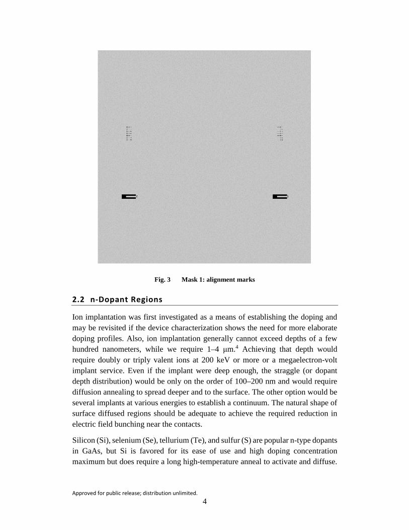
Approved for public release; distribution unlimited. 4
Fig. 3 Mask 1: alignment marks
2.2 n-Dopant Regions
Ion implantation was first investigated as a means of establishing the doping and may be revisited if the device characterization shows the need for more elaborate doping profiles. Also, ion implantation generally cannot exceed depths of a few hundred nanometers, while we require 1–4 μm.4 Achieving that depth would require doubly or triply valent ions at 200 keV or more or a megaelectron-volt implant service. Even if the implant were deep enough, the straggle (or dopant depth distribution) would be only on the order of 100–200 nm and would require diffusion annealing to spread deeper and to the surface. The other option would be several implants at various energies to establish a continuum. The natural shape of surface diffused regions should be adequate to achieve the required reduction in electric field bunching near the contacts.
Silicon (Si), selenium (Se), tellurium (Te), and sulfur (S) are popular n-type dopants in GaAs, but Si is favored for its ease of use and high doping concentration maximum but does require a long high-temperature anneal to activate and diffuse.

Approved for public release; distribution unlimited. 5
Se and Te have lower diffusion coefficients than Si (requiring higher temperatures and/or longer anneal times), but S diffuses rapidly and may be a good alternative.
The high-temperature anneal for Si of 800–850 °C for 12–24 h requires either an arsenic (As) over pressure or a capping layer be used to prevent As loss via evaporation starting at approximately 550 °C. I chose plasma-enhanced chemical vapor deposited (PECVD) silicon nitride (SiNx) over silicon oxide because it prevents As loss better. PECVD SiNx has a lot of hydrogen (H) in it as-grown and it densifies as the H leaves when annealed above approximately 500 °C. This densification causes the film to contract, becoming tensile. The final deposition recipe shown in the Appendix, Section 2 was found after numerous trials and results in a minimum between compressive stress bubble and hash-mark or crack tensile defects. The ammonia (NH3) to silane (SiH4) ratio optimizes the index to a SiNx slightly rich in Si over the stoichiometric Si3N4 composition. The helium (He) to nitrogen (N2) gas ratio and pressure have a larger effect on the stress of the film than does the SiH4 to NH3 ratio.5 The high 300 °C could ideally be a bit higher (350 °C) to improve the as-deposited density, but 350 °C is the tool’s maximum and was avoided. The liftoff process was experimentally found to be higher yield than a base SiNx film with windows etched in it, followed by an a-Si blanket deposition, followed by a SiNx cap layer. The NH3 pretreatment vastly improves the film’s adhesion to the GaAs surface,6 and an oxygen (O2) plasma clean often used to remove photoresist remnants after liftoff was omitted, as it causes the a-Si patches to delaminate the SiNx cap during the high-temperature diffusion anneal.
The full procedure is detailed with cross-sectional illustrations in Section A-2 of the Appendix, while Fig. 4 shows the plan view of the Si patches. Initially, attempts were made to strip the annealed SiNx film along with the a-Si layer before applying another SiNx masking layer for the p-type dopant process, but the concentrated 49% hydrogen fluoride (HF) required to strip the annealed Si adversely affects the GaAs surface and uncontrollably etches the AlGaAs epilayer. As seen later in Section 2.4, the annealed SiNx and a-Si layers are removed after the p-dopant process is complete to allow the existing annealed SiNx layer to be used as both a p-dopant diffusion mask and as part of the final AR coating.

Approved for public release; distribution unlimited. 6
Fig. 4 Mask 2: n-doping regions in turquoise (overlaying previous pattern)
2.3 p-Dopant Regions
Carbon, beryllium, magnesium, zinc (Zn), and cadmium are common GaAs p-type dopants. Zn was chosen as it has a high diffusion coefficient (can be diffused readily at low temperatures) and has a high maximum achievable concentration. Zn may be diffused into the surface through Zn vapor overpressures in a sealed ampoule inside a diffusion furnace, implanted, or via a Zn containing film coating. Zn also has just a high diffusion coefficient that it is often not allowed in cleanroom equipment such as evaporators and furnaces. To comply with this requirement, I chose to use a Zn containing spin on diffusant glass (Zn: spin on diffusant [SOD]).7 The top SiNx coating was experimentally found to be necessary at 700 °C and likely necessary for 600 °C. As shown in Section A-3 of the Appendix, concentrated HF readily penetrates the top low-temperature annealed SiNx cap lifting off to strip the Zn:SOD. The short amount of time that the concentrated HF is in contact with the lower high-temperature annealed SiNx causes minimal etching and does not visibly affect the AlGaAs epilayer. Figure 5 shows the plan view of the p-doping regions in violet.

Approved for public release; distribution unlimited. 7
Fig. 5 Mask 3: p-doping regions in violet (overlaying previous patterns)
2.4 Contacts
At this stage, the p-type doped regions are exposed, but the n-type regions are still covered with a-Si and SiNx, and the intrinsic contact regions are covered with just SiNx. This situation requires that each be removed in succession, as the n-type region needs extra etching time to remove the a-Si as shown in Section A-4 of the Appendix. A new mask was not generated to etch the a-Si windows, as the n-type region mask could be reused by overexposing it. The overexposure reduces the window width preventing GaAs outside the doped region from being etched during the a-Si etch duration.
The intrinsic contact region windows are etched in the SiNx separately, as shown in Section A-5 of the Appendix with a cross-sectional illustration (Fig. A-11) and in a plan view (in orange) in Fig. 6.

Approved for public release; distribution unlimited. 8
Fig. 6 Mask 4: intrinsic device contact window regions in orange (overlaying previous patterns)
Initially, palladium (Pd)/gold (Au) contacts were investigated to provide a means of contacting to both the n- and p-type regions at once, with the thought being that the typical dopants added to metal contact stacks would not be necessary because of the high surface dopant concentrations generated by the surface diffusion process. The surface Fermi pinning of GaAs causes n-type GaAs to be more difficult to form low-resistance ohmic contacts to than p-type. Experiments showed that Pd/germanium (Ge)/Au contacts8 work best for n-type GaAs and adequately provide ohmic contact to p-type GaAs as implemented in Section A-6 of the Appendix.
Figure 7a shows a plan view of the common n- and p-type contacts, while Fig. 7b shows a close up of one of the contact pads. The metal boarders are 10-μm interior to the defined dopant region boarders.

Approved for public release; distribution unlimited. 9
(a)
(b)
Fig. 7 a) Mask 5: metal contact regions in red (overlaying previous patterns) and b) close up of p/n device (showing diffused dopant border in blue)
After the contact metal has been applied, the annealed SiNx thickness is measured using an optical reflectometer. This thickness measurement and reflectance null wavelength are used to determine the optimal top AR SiNx coating thickness

Approved for public release; distribution unlimited. 10
applied in Section A-7 of the Appendix. The contacts are annealed and windows must then be etched through the SiNx AR coating to make contact to the Au contact pads. To reduce the risk of any metallization damage that may occur in operation, the windows are opened interior to the metal pad borders as shown in Fig. 8a and b.
(a)
(b)
Fig. 8. a) Close up of mask 6: AR cap window for p-type region in field of purple (showing opening is set inside contact metal border) and b) microscope image of the same

Approved for public release; distribution unlimited. 11
Figure 9 shows a representative completed p/n PCSS device ready for packaging.
Fig. 9 Microscope image of a completed p/n device
2.5 Packaging
Early device packaging efforts revealed several important challenges. These devices are biased at or beyond the air breakdown field strength of 3 × 10⁴ V/cm. Without a transparent high-dielectric strength coating material, the devices would simply flash over before proper bias was achieved. Dielectric oils were initially investigated, but I settled on a solid-state silicone dielectric gel encapsulant with a dielectric strength of 1.7 × 10⁵ V/cm.9
Section A-8 in the Appendix lays out the process for the final packaging solution. The devices are wirebonded to package lead bond pads, as soldering directly to the device contacts would dissolve the thin Au device metallization. Shown in Fig. 10 is an interim packaging solution for testing bars of devices, which was readily available and lacks the typical metal backplane seen in modern semiconductor packages. Metal backplanes act as floating contacts that can easily provide a shorting path between package leads, due to the close proximity of the wirebonds and package bond pads to any metal backplane. Leakage current passing through biased PCSS devices cause heating, which must be dissipated by the package and

Approved for public release; distribution unlimited. 12
die bonding material. The die bonding material chosen is a 2-part silver-filled conductive epoxy, which when applied must remain interior to the footprint of the device so as not to act as a miniature metal backplane.
Fig. 10 Microscope image of a bar of test devices in a package
3. Conclusions
Test bars of devices have been packaged (similar to Fig. 10) and will be characterized using a nanosecond pulsed laser. The optoelectronic behavior of these devices across various high-voltage bias levels will be used to compare the speed and response of each doping type (intrinsic, p/n, n/n, and p/p) across each substrate case (undoped GaAs case A and AlGaAs/GaAs cases B and C).
The final process reported here has successfully fabricated and packaged devices, though minor dopant diffusion or other process variations may be warranted based on optoelectronic behavior.

Approved for public release; distribution unlimited. 13
4. References
1. Mar A, Loubriel GM, Zutavern FJ, O’Malley MW, Helgeson WD, Brown DJ, Hjalmarson HP, Baca AG, Thornton RL, Donaldson RD. IEEE Trans Plasma Science. 2000;28(5):1507.
2. Persall TP, Capasso F, Nahory RE, Pallack MA, Chelikowsky J. Solid State Electron. 1978;21(1):297.
3. Kyuregyan AS, Yurkov SN. Sov Phys Semicond. 1989;23(10):1126.
4. Schubert EG. Doping in III-V semiconductors. New York (NY): Cambridge University Press; 1993.
5. Mackenzie KD, Khanna R, Jacob J. Proceedings of CS MANTECH Conference, Boston, MA, 2012.
6. Wang T. Proceedings of the CS MANTECH Conference, Tampa, FL, 2009.
7. Filmtronics: Spin-on diffusant, zinc film—product code 980. Butler (PA): Filmtronics Inc.; 2004 Jul [accessed 2016 Sep]. http://www.pdx.edu/pnna /sites/www.pdx.edu.pnna/files/Spin-On%20Diffusants___Catalog_Version -%206.pdf.
8. Hao PH, Wang LC, Deng Fei, Lau SS, and Cheng JY. J Applied Physics. 1996;79:4211.
9. Dow Corning: Sylgard 527 silicone dielectric gel. Auburn (MI): Dow Corning Corp.; 2016 [accessed 2016 Sep]. http://www.dowcorning.com/applications /search/default.aspx?R=229EN.

Approved for public release; distribution unlimited. 14
INTENTIONALLY LEFT BLANK.

Approved for public release; distribution unlimited. 15
Appendix. Detailed Fabrication Process

Approved for public release; distribution unlimited. 16
What follows is the detailed fabrication process described in Section 2.
Note: See the List of Symbols, Abbreviations, and Acronyms for definitions of terms used in this Appendix.
A-1 Define Alignment Marks
1) Pattern alignment marks mask (align to sample edges).
a) Negative tone PR
AZ5214E 4000 RPM, 60 s, fastest acceleration
Hotplate 110 °C for 1 min
MA6 HARD CONTACT expose 2.5 s (9 mW/cm2)
Hotplate 120 °C actual for 2 min
MA6 FLOOD expose 30 s
Develop in MIF 300 for 50 s
Etch alignment marks
b) ULVAC etch: 500-W ICP, 50-W RIE, 4 mT, 16-sccm BCl3, 4-sccm Ar, 12 s (~50 nm)
GaAs etches at 7.54 nm/s after 6-s etch delay. PR etches at 8.66 nm/s.
c) Strip PR
Acetone soak, propanol rinse, N2 dry
O2 plasma strip 15 min
d) BOE dip 30 s
Fig. A-1 Etched alignment profile
A-2 Define N-Dopant Regions
2) Pattern n-dopant windows PR (alignment mark 1)

Approved for public release; distribution unlimited. 17
a) Negative tone PR
AZ5214E 4000 RPM, 60 s, fastest acceleration
Hotplate 110 °C for 1 min
MA6 HARD CONTACT expose 2.5 s (9 mW/cm2)
Hotplate 120 °C actual for 2 min
MA6 FLOOD expose 30 s
Develop in MIF 300 for 50 s
Etch alignment marks
3) Evaporate a-Si
a) E-beam evaporate 1000 Å Si
4) Liftoff PR
a) Acetone soak, propanol rinse, N2 dry
Fig. A-2 a-Si regions patterned
5) Deposit SiNx cover
a) PECVD for 16 min (~200 nm):
48 NH3, 1000 He, 50 W, 300 °C, 900 mT, 30-s pretreatment
500-sccm SiH4, 15-sccm NH3 (n= ~2.1), 750 He, 250 N2, 50 W, 300 °C, 900 mT
Fig. A-3 Base SiNx protectant cover applied

Approved for public release; distribution unlimited. 18
6) Anneal at 850 °C 12 h with N2
Fig. A-4 The n-type dopant regions diffused
A-3 Define P-Dopant Regions
1) Pattern p-dopant windows PR (alignment mark 2)
a) HMDS 4000 RPM, 60 s, fastest acceleration
b) Negative tone PR
AZ5214E 4000 RPM, 60 s, fastest acceleration
Hotplate 110 °C for 1 min
MA6 HARD CONTACT expose 2.5 s (9 mW/cm2)
Hotplate 120 °C for 2m
MA6 FLOOD expose 30 s
Develop MIF 300 for 50 s
2) Etch annealed SiNx windows
a) 30-sccm CF4, 2-sccm O2, 5 mT, 100-W bias, 500-W ICP, 46 s (~215 nm)
b) Annealed SiNx etches at 5.44 nm/s + 6-s delay. GaAs underneath etches at 1.5 nm/s.
3) Strip PR
a) Acetone soak, propanol rinse, N2 dry
b) O2 plasma 15 min

Approved for public release; distribution unlimited. 19
Fig. A-5 The p-type region windows opened in annealed SiNx cover
4) Deposit Zn:SOD
a) Spin at 3000 RPM, max acceleration, 60 s
b) Hotplate 250 °C for 15 min
Fig. A-6 The p-type with Zn:SOD applied
5) Deposit SiNx cover
a) PECVD for 16 m (~200 nm):
48 NH3, 1000 He, 50 W, 300 °C, 900 mT, 30-s pretreatment
500-sccm SiH4, 15-sccm NH3 (n= ~2.1), 750 He, 250 N2, 50 W, 300 °C, 900 mT
Fig. A-7 Temporary SiNx cover applied, encapsulating Zn:SOD
6) Anneal p-dopant
a) 600 °C 30 min in N2

Approved for public release; distribution unlimited. 20
Furnace is actually greater than 575 °C for 1.25 h (>550 °C for 1.5 h).
Fig. A-8 The p-type dopant regions diffused
7) Lift off SOD and top SiNx cover in HF
a) 49% HF 30 s
b) spray hard with water to remove SiNx remnants
c) 49% HF 30 s more
d) spray hard with water to remove any remaining SiNx particles
e) N2 dry
This short duration has not affected AlGaAs surface.
Fig. A-9 Zn:SOD and temporary SiNx cover removed
A-4 Define N-Dopant Trenches
1) Overexpose n-dopant windows PR (alignment mark 1)
a) HMDS 4000 RPM, 60 s, fastest acceleration
b) Negative Tone PR
AZ5214E 4000 RPM, 60 s, fastest acceleration
Hotplate 110 °C for 1 min

Approved for public release; distribution unlimited. 21
MA6 HARD CONTACT expose 6 s (9 mW/cm2)
Hotplate 120 °C for 2 min
MA6 FLOOD expose 30 s
Develop MIF 300 for 50 s
2) Etch annealed SiNx windows and Si
a) 30-sccm CF4, 2-sccm O2, 5 mT, 100-W bias, 500-W ICP, 60 s
Annealed SiNx etches at 5.44 nm/s + 6-s delay, then 5.8 nm/s for annealed a-Si. GaAs underneath etches at 1.5 nm/s.
3) Strip PR
a) Acetone soak, propanol rinse, N2 dry
b) O2 plasma strip 15 min
Fig. A-10 The n-type region windows opened in annealed SiNx cover and a-Si
A-5 Define Intrinsic Device Regions
1) Pattern intrinsic contact regions PR (alignment mark 6)
a) HMDS 4000 RPM, 60 s, fastest acceleration
b) Negative tone PR
AZ5214E 4000 RPM, 60 s, fastest acceleration
Hotplate 110 °C for 1 min
MA6 HARD CONTACT expose 2.5 s (9 mW/cm2)
Hotplate 120 °C for 2 min
MA6 FLOOD expose 30 s
Develop MIF 300 for 50 s

Approved for public release; distribution unlimited. 22
2) Etch annealed SiNx windows
a) 30-sccm CF4, 2-sccm O2, 5 mT, 100-W bias, 500-W ICP, 46 s (~215 nm)
Annealed SiNx etches at 5.44 nm/s + 6-s delay. GaAs underneath etches at 1.5 nm/s.
3) Strip PR
a) Acetone soak, propanol rinse, N2 dry
b) O2 plasma strip 15 min
4) BOE dip 30 s
Fig. A-11 Intrinsic region windows opened in annealed SiNx cover
A-6 Define Contacts
1) Pattern common contact windows PR (alignment mark 3)
a) HMDS 4000 RPM, 60 s, fastest acceleration
b) Negative tone PR
AZ5214E 4000 RPM, 60 s, fastest acceleration
Hotplate 110 °C for 1 min
MA6 HARD CONTACT expose 2.5 s (9 mW/cm2)
Hotplate 120 °C for 2 min
MA6 FLOOD expose 30 s
Develop MIF 300 for 50 s
2) E-beam evaporate 100 Å Pd / 300 Å Ge / 3000 Å Au
3) Lift off PR

Approved for public release; distribution unlimited. 23
a) Acetone soak, propanol rinse, N2 dry
b) O2 plasma strip 15 min
Fig. A-12 Contact metal deposited
A-7 Define AR Cap
1) Deposit AR cap
a) Measure annealed SiNx thickness
With 190 nm of existing SiNx, one needs (3/2 + 0.25)*510/2.05–190 = 245 nm more at 12.6 nm/min.
b) Deposit SiNx to reach next AR null.
Fig. A-13 AR coating applied
2) Anneal contacts 330–340 °C 30 min with N2.
3) Pattern cap windows PR (alignment mark 5)
a) HMDS 4000 RPM, 60 s, fastest acceleration
b) Negative Tone PR
AZ5214E 4000 RPM, 60 s, fastest acceleration
Hotplate 110 °C for 1 min
MA6 HARD CONTACT expose 2.5 s (9 mW/cm2)

Approved for public release; distribution unlimited. 24
Hotplate 120 °C for 2 min
MA6 FLOOD expose 30 s
Develop MIF 300 for 50 s
4) Etch unannealed SiNx cap
a) 30-sccm CF4, 2-sccm O2, 5 mT, 100-W bias, 500-W ICP, 46 s (~215 nm)
Unannealed SiNx etched at 5.63 nm/s + 6 s. Au underneath etches negligibly.
5) Strip PR
a) Acetone soak, propanol rinse, N2 dry
b) O2 plasma strip 15 min
Fig. A-14 AR coating windows opened, completing device fabrication
A-8 Package Devices
1) Dice devices
a) deposit blue protectant for dicing
spin FSC-M at 3000 RPM for 60 s
cure in 90 °C oven for 30 min
b) dice 625-μm ±25-μm-thick devices
2) Mount devices and Au-coated Kovar strips on AlO2 bases
a) 1:1 silver conductive epoxy
b) cure in 90 °C oven for 30 min

Approved for public release; distribution unlimited. 25
3) Wirebond devices
a) 1-mil Au ball bonding
4) Reinforce wirebonds to package pads
a) mix and apply 1:1 silver conductive epoxy
b) cure in 90 °C oven for 30 min
5) Attach 3-D printed encapsulant dam
a) mix 2-parts Loctite M-31CL Hysol Medical Device Epoxy and coat inside (to seal any pores) and bottom of 3-D printed part
b) cure at room temperature for 4 h
6) Encapsulate in potting material
a) Mix 1:1 Sylgard 527 silicone dielectric gel
b) Degas gel for a few minutes at –20 psig or better
c) Cure in 90 °C oven for at least 3.5 h

Approved for public release; distribution unlimited. 26
List of Symbols, Abbreviations, and Acronyms
3-D 3-dimensional
AlGaAs aluminum gallium arsenide
AlO2 sapphire
AR anti-reflection coating
Ar argon
As arsenic
Au gold
BCl3 boron trichloride
BOE buffered oxide etch
FSC-M Dow Electronic Materials MICROPOSIT FSC surface coating, M thickness
GaAs gallium arsenide
Ge germanium
He helium
HF hydrogen fluoride
ICP inductively coupled plasma
MBE molecular beam epitaxy
MIF metal ion free
N2 nitrogen
NH3 ammonia
O2 oxygen
PCSS photoconductive semiconductor switch
Pd palladium
PECVD plasma enhanced chemical vapor deposition
PR photoresist
RIE reactive ion etcher

Approved for public release; distribution unlimited. 27
S sulfur
Se selenium
Si silicon
SiH4 silane
SiNx silicon nitride (non-stoichiometric)
Te tellurium
Zn zinc
Zn:SOD Zn-doped spin on diffusant

Approved for public release; distribution unlimited. 28
1 DEFENSE TECH INFO CTR (PDF) DTIC OCA 2 US ARMY RSRCH LAB (PDF) IMAL HRA MAIL & RECORDS MGMT RDRL CIO L TECHL LIB 1 GOVT PRNTG OFC (PDF) A MALHOTRA 4 US ARMY RSRCH LAB (PDF) RDRL SEE G WOOD RDRL SEE I J BICKFORD RDRL SEE L A MOTT R C HOFFMAN