Embed Size (px)
Citation preview

Microwave Balanced Oscillators and
Frequency Doublers
Nipapon Siripon
Submitted for the Degree of Doctor of Philosophy
from the University of Surrey
Uni
Advanced Technology Institute School of Electronics and Physical Sciences
University of Surrey Guildford, Surrey GU2 7XH, UK
August 2002
© Nipapon Siripon

Abstract
The research presented in this thesis is on the application of the injection-locked oscillator
technique to microwave balanced oscillators. The balanced oscillator design is primarily
analysed using the extended resonance technique. A transmission line is connected
between the two active devices, so that the active device resonate each other. The
electrical length of the transmission line is also analysed for the balanced oscillation
condition.
The balanced oscillator can be viewed with the negative resistance model and the
feedback model. The former model is characterised at a circuit plane where the feedback
network is cut. By using both the negative-resistance oscillator model and the feedback
model, the locking range of the oscillator is analysed by extending Kurokawa's theory.
This analysis demonstrates the locking range of the injection phenomenon, where the
injection frequency is either close to the free-running frequency, close to (lin) x free
running frequency or close to n x the free-running frequency. It also reveals the effect of
different injection power levels on the locking range. Injection-locked balanced
oscillators for subharmonic and fundamental modes are constructed. When the balanced
oscillator is in the locking state, it is clearly shown that the output signal is better
stabilised and the phase noise is attenuated. The experimental results agree with the
analysis. Furthermore, the spurious signal suppression in a cascaded oscillator is
investigated.
The other focus of this research is on the design of frequency doublers. A balanced
douber is designed and integrated with a balanced injection-locked oscillator. The
experimental result shows that the output signal is clean and stabilised. The other
important frequency doubler design technique studied is the use of the feedforward
technique to significantly eliminate the fundamental frequency component. The design
and the experiment show that the fundamental component can be suppressed to better
than 50 dBc.
Key words: injection-locked oscillator, locking range, phase noise, frequency doubler,
feedforward technique.
11

Acknowledgements
I am indebted to my family, especially my mother, for their encouragement.
I wish to express my gratitude to my supervisor, Prof. I D. Robertson, for guidance during
doing this work. I am really grateful to Prof. M.J.Underhill for all his suggestion,
guidance and also valuable discussions. Also, I would like to thank Dr.S.Lucyszyn and
Prof. C.S.Aitchison for their help and suggestions.
I would like to express my appreciation to Dr.K.S.Ang for the great support, suggestions
and discussion on balanced oscillator design.
I am grateful to the Thai government for financial support. I would like to acknowledge
Mr.D.Granger and the Electronics Workshop and the Teaching Lab staff for their
supports.
I would like to knowledge the support of my friends: Dr.P.Asadamongkon,
Dr.S.Chuichu1cherm, Dr.S.Panyametheekul, Miss S.Daungkeaw, Miss K.Dankhonsakul,
Miss W.Usaha, Miss A.Pungnim, Mr.A.Butsayakul, Mr.A.Sangthanavanit and Miss
T. Tangmahasuk.
Finally, I would like to thank Mrs.L.Tumilty for her secretarial support and I would like
to acknowledge to Dr.S.Nam, Dr.D.McPherson, Dr.M.Chongcheawchamnan,
Mr.C.Chrisostomidis, Mr.S.Bunjaweht, Mr.M.Aftanasar, Mr.C.Y.Ng, Mr.J.Wong for
their helpful support.
IV

Contents
Contents
Abstract ........................................................................................................................... ii
Acknowledgements ......................................................................................................... iv
Contents .......................................................................................................................... v
L· fP' ... 1st 0 19ures .............................................................................................................. Vll1
List of Tables ................................................................................................................. xii
Chapter 1 ......................................................................................................................... 1
1 Introduction ............................................................................ : ..................................... 1
Chapter 2 ......................................................................................................................... 4
2 Balanced Oscillators ..................................................................................................... 4
2.1 Introduction .......................................................................................................... 4
2.2 Oscillation conditions ........................................................................................... 5
2.3 Balanced oscillator analysis .................................................................................. 8
2.4 A self-oscillating balanced mixer ....................................................................... 24
2.4.1 Design considerations for a balanced mixer .................................................. 25
2.4.2 Circuit realisation ......................................................................................... 26
2.4.3 Results and discussion .................................................................................. 29
2.5 Conclusion ......................................................................................................... 31
Chapter 3 ....................................................................................................................... 33
3 Injection-Locked Balanced Oscillators ........................................................................ 33
3.1 Introduction ........................................................................................................ 33
v

Contents
3.2 Phase noise theory .............................................................................................. 34
3.3 Injection-locked oscillator theory ....................................................................... 40
3.4 Design considerations for the injection-locked balanced oscillator ..................... .49
3.5 Circuit Realisations ............................................................................................ 50
3.6 Results and discussion ........................................................................................ 51
3.6.1 Fundamental injection-locked balanced oscillator. ........................................ 51
3.6.2 Sub-harmonic injection-locked balanced oscillator ....................................... 58
3.7 Conclusion ......................................................................................................... 61
Chapter 4 ....................................................................................................................... 64
4 Injection-locking applied to a cascaded oscillator. ....................................................... 64
4.1 Introduction ........................................................................................................ 64
4.2 Design considerations for the injection-locked cascaded oscillator ..................... 65
4.3 Circuit realisation ............................................................................................... 66
4.4 Results and discussion ........................................................................................ 67
4.5 Conclusion ......................................................................................................... 74
Chapter 5 ....................................................................................................................... 75
5 Frequency Doubler Design Considerations ................................................................. 75
5.1 Introduction ........................................................................................................ 75
5.2 General Doubler Design Considerations ............................................................. 76
5.2.1 Biasing considerations .................................................................................. 77
5.2.1.1 V gs near pinch-off (Class B) .................................................................... 80
5.1.0.2 V gs in the vicinity of forward conduction and between 0 volt and pinch-
off ................................................................................................................ 81
5.2.2 Frequency doubler design topologies ........................................................... 82
5.2.2.1 Single-ended frequency doubler ................................................................ 82
5.2.2.2 Balanced frequency doublers .................................................................... 83
5.3 Practical example of an injection-locked balanced oscillator and doubler ........... 84
5.3.1 Circuit realisation ......................................................................................... 84
5.3.2 Results and Discussion ................................................................................. 87
5.4 Conclusion ......................................................................................................... 90
VI

Contents
Chapter 6 ....................................................................................................................... 91
6 Frequency Doubler using Feedforward Technique ...................................................... 91
6.1 Introduction ........................................................................................................ 91
6.2 Design ................................................................................................................ 93
6.3 Circuit Realisations ............................................................................................ 95
6.3.1 Single-ended Doubler Design ....................................................................... 95
6.3.2 Reflection-type analogue phase shifter and directional coupler ..................... 98
6.4 Results and discussion ........................................................................................ 99
6.5 Conclusion ....................................................................................................... 104
Chapter 7 ..................................................................................................................... 105
7 Conclusions and Suggestions for Future Work .......................................................... 105
References ................................................................................................................... 110
VII

List of Figures
List of Figures
Figure 2- 1: A simple negative-feedback oscillator model ................................................ 5
Figure 2- 2: a) A microwave oscillator circuit, b) its signal flow graph ............................ 6
Figure 2- 3: a) Negative resistance oscillator, b) Two-port negative resistance approach .. 7
Figure 2- 4: a) The balanced oscillator architecture, b) its equivalent circuit.. ................... 8
Figure 2- 5: The Smith chart shows load and input impedance for the extended resonance
technique ......................................................................................................................... 9
Figure 2- 6: a) A negative-resistance balanced oscillator, b) its transformed feedback
oscillator ........................................................................................................................ 11
Figure 2- 7: An equivalent circuit of the negative-resistance technique .......................... 12
Figure 2- 8: The block diagram of the balanced oscillator .............................................. 19
Figure 2- 9: The signal flow graph of the balanced oscillator ......................................... 21
Figure 2- 10: The basic building block of a singly balanced FET mixer ......................... 26
Figure 2- 11: A block diagram of the Balanced Self-Oscillating Mixer .......................... 27
Figure 2- 12: A circuit diagram of the Balanced Self-Oscillating Mixer ......................... 28
Figure 2- 13: Simulated performance of return loss at RF .............................................. 28
Figure 2- 14: The anti-phase IF signals at the two outputs .............................................. 29
Figure 2- 15: Measurement set-up .................................................................................. 30
Figure 2- 16: Conversion gain vs. input power .............................................................. 30
Figure 3- 1: AM and FM components ............................................................................ 35
Figure 3- 2: Vector diagram of a carrier simultaneously phase and amplitude modulated
by the nth noise voltage interference .............................................................................. 36
Figure 3- 3: Spectrum of source in frequency domain .................................................... 37
Figure 3- 4: Leeson's model .......................................................................................... 37
Figure 3- 5: a) A equivalent circuit for the oscillator, b) equivalent circuit characterised in
both negative and feedback models and c) equivalent oscillator on right-hand side of the
balanced oscillator ......................................................................................................... 43
Figure 3- 6: The proposed injection-locked balanced oscillator configuration ................ 50
Figure 3- 7: The fundamental injection-locked balanced oscillator circuit ...................... 51
viii

List of Figures
Figure 3- 8: The sub-harmonic injection-locked balanced oscillator circuit .................... 51
Figure 3- 9: The measured free-running signal compared to the injection locking
frequency signals ........................................................................................................... 52
Figure 3- 10: The locking range of the fundamental injection-locked balanced oscillator
as function of the injection power level. ......................................................................... 53
Figure 3- 11: Experimental set -up for phase and magnitude measurement of the injection-
locked balanced oscillator output ................................................................................... 54
Figure 3- 12: The amplitude and phase response between two output ports of the ILBO as
locking on polar diagram ............................................................................................... 55
Figure 3- 13: a) Magnitude and b) Phase response of the fundamental injection-locked
balanced oscillator ......................................................................................................... 56
Figure 3- 14: The output signals between fundamental and harmonic injection-locked
balanced oscillator ......................................................................................................... 57
Figure 3- 15: The measured sub-harmonic injection locked frequency signal ................. 59
Figure 3- 16: The locking range as a function of the injection power .............................. 59
Figure 3- 17: Phase measurement test bench setup for sub-harmonic injection-locked
balanced oscillator ......................................................................................................... 60
Figure 3- 18: Measured phase difference between the two outputs of the sub-harmonic
injection-locked balanced oscillator ............................................................................... 61
Figure 4- 1: A block diagram of a cascaded oscillator .................................................... 65
Figure 4- 2: A single-ended oscillator circuit ................................................................. 66
Figure 4- 3: The cascaded oscillator circuit.. .................................................................. 67
Figure 4- 4: Free-running cascaded oscillator output without injection signal. ................ 68
Figure 4- 5: The output signal from the injection-locked cascaded oscillator: the injection
frequency is close to lx, (l/2)x and (l/3)x free-running frequency ................................. 68
Figure 4- 6: The output signal from the injection-locked single-ended oscillator: the
injection frequency is close to lx, (l/2)x and (1/3)x free-running frequency .................. 69
Figure 4- 7: The output spectrum from the single-ended oscillator during locking state
with respect to the injection signal at frequency of (1/2) x free-running oscillating signal
...................................................................................................................................... 70
IX

List of Figures
Figure 4- 8: The output spectrum from the single-ended oscillator during locking state
with respect to the injection signal at frequency of (1/3) x free-running oscillating signal
...................................................................................................................................... 70
Figure 4- 9: The output spectrum from the cascaded oscillator during locking state with
respect to the injection signal at frequency of (l/2)x free-running oscillating signal ....... 72
Figure 4- 10: The output spectrum from the cascaded oscillator during locking state with
respect to the injection signal at frequency of (l/3)x free-running oscillating signal ....... 73
Figure 5- 1: a) The physical form and b) the nonlinear model of the GaAs MESPETs .... 78
Figure 5- 2: PET output characteristics showing the region of operation for frequency
doubler operation ........................................................................................................... 80
Figure 5- 3: Waveforms and signal trajectory for class B multiplier ............................... 81
Figure 5- 4: The frequency doubler employing A / 4 transmission lines ......................... 82
Figure 5- 5: A balanced (push-push) doubler ................................................................. 83
Figure 5- 6: The circuit diagram of the novel sub-harmonic injection-locked balanced
oscillator-doubler configuration ..................................................................................... 85
Figure 5- 7: Single-ended doubler circuit configuration ................................................. 86
Figure 5- 8: The Wilkinson power divider ...................................................................... 87
Figure 5- 9: The output spectrum of the balanced oscillator-doubler circuit (with 3-dB
attenuator and without sub-harmonic injection-locking signal 0.5-dB cable loss at the
output) ........................................................................................................................... 88
Figure 5- 10: The comparison between the output of the balanced oscillator-doubler, with
and ................................................................................................................................. 89
Figure 5- 11: The measured locking range of the subharmonic injection-locked oscillator-
doubler as a function of injection power level ................................................................ 89
Figure 6- 1: Feedforward technique for a linearised power amplifier. ............................. 92
Figure 6- 2: Feedforward technique for fundamental signal suppression in a frequency
doubler .......................................................................................................................... 94
Figure 6- 3: Single-ended doubler circuit configuration ................................................. 95
Figure 6- 4: Single-ended doubler circuit ....................................................................... 96
Figure 6- 5: Filter configuration ..................................................................................... 97
Figure 6- 6: Simulation result of the filter ...................................................................... 97
x

List of Figures
Figure 6- 7: The reflection-type phase shifter configuration ........................................... 98
Figure 6- 8: The layout of reflection-type phase shifter at 10Hz .................................... 98
Figure 6- 9: The measurement result of the filter from the network analyzer .................. 99
Figure 6- 10: Output spectrum of the I-to-20Hz doubler without the feedforward
technique (with a 3-dB attenuator and 0.5-dB cable loss at the ouput) .......................... 100
Figure 6- 11: Phase and insertion loss of phase shifter ................................................. 101
Figure 6- 12: Output of the 1-2 GHz doubler with feedforward (with a 3-dB attenuator
and 0.5-dB cable loss at the ouput) ............................................................................... 102
Figure 6- 13: Measured output of the frequency doubler as a function of the input power
level. ............................................................................................................................ 102
Figure 6- 14: Feedforward technique for odd harmonic component suppression in
frequency doubler ........................................................................................................ 103
Figure 7- 1: Concept of the power dissipation and phase noise ..................................... 108
Figure 7- 2: A distributed oscillator ............................................................................. 108
Xl

List of Tables
List of Tables
Table 2- 1: The input and load coefficients with respect to different frequencies ............ 23
Table 2- 2: The length of the transmission line by simulation and calculation for different
frequencies .................................................................................................................... 24
Table 3- 1: The locking range with respect to the fundamental and harmonic injection-
locked balanced oscillator at power levels of -7.5 and -20 dBm .................................... 57
Table 4- 1: The locking range with respect to the injection power levels, where the
injection frequency is close to (l/2)x free-running frequency ......................................... 71
Table 4- 2: The locking range with respect to the injection power level, where the
injection frequency is close to (l/3)x free-running frequency ......................................... 71
Table 4- 3: The locking range for the single-ended oscillator with respect to the injection
power levels, where the injection frequency is close to (l/2)x free-running frequency ... 73
Table 4- 4: The locking range for the cascaded oscillator with respect to the injection
power levels, where the injection frequency is close to (l/3)x of free-running frequency74
Xll

Glossary of temlS
Glossary of Terms
N out
L«())m)
(S I N)in
(SIN)out
~8 nns,total
Ppavai/,nns
~8nns
Noise power applied at the output of the amplifier
Reactive energy going between Land C
Lowpass transfer function
Signal-to-noise ratio at the input of the amplifier
Signal-to-noise ratio at the output of the amplifier
Total phase deviation
Arbitrary phase angle
Available rms signal power
Equivalent available noise voltage due to the noise figure in the
amplifier
Angle of SIt
Capacitor charge on cpapcitor
External quality factor
Locking range
Noise power applied at the input of the amplifier
Phase deviation
Phase noise
Power dissipated in the resonator
Spectral density at the frequency at an offset frequency
Carrier voltage
Xll

F
11
81
82
Qc
lIN(jCO)
IL(jCO)
8T
IT
A(jco)
L
AM
Cds
Cgd
cgs
D
Frequency from the carrier
Modulation index
Noise figure
Noise voltage
Frequency in radian
Subtracting symbol
Phase of current in a balanced oscillator
Phase of current in a balanced oscillator
Carrier frequency in radian
Input coefficient
Load coefficient
Glossary of tenns
Electrical length of the transmission line in the terminating network
Terminating coefficient
Gain of the amplifier
Adding symbol
A growing signal
Amplitude modulation
A small noise signal generated in the circuit
Transfer function of resonator element
Capacitance
Drain-source capacitance
External capacitance
Gate-source capacitance
Gate-drian capacitance
Drain
xiii

dB
dBc
dBm
DC
e
fo
FET
PM
G
G
g
GaAs
GHz
HP
I(t)
IBLO
Id
IF
K
K
L
LMDS
Glossary oj temlS
Decibel
Decibel relative to carrier
Decibel relative to 1 mW
Direct current
Electrical length of the transmission line in a balanced oscillator
Operating frequency
Corner frequency
Field effect transistor
Offset frequency
Frequency Modulation
Gate
gain of the amplifier
Nonlinear function of active device
Gallium Arsenide
Drain-source transconductance
Gigahertz
Transconductance
Hewlett Packard
Current
Injection-locked balanced oscillator
Drain current
Intermediate frequency
Stability factor
Boltzmann's constant
Indactance
Local Multi-point Distribution Systems
xiv

LO
MESFET
MHz
q
Q
R
Rd
RF
Rg
Ri
RIN
RL
Rs
S
S
SIBLO
SSB
t
T
Vet)
Vd
Vds
Vg
Vgs
Glossary of tenns
Local oscillator
Metal Semiconductor Field Effect Transistor
Megahertz
Charge in Coulomb
Loaded quality factor
Resistance
Drain resistance
Radio frequency
Gate resistance
Resistance of the semiconductor region under the gate
Input resistance
Load resistance
Source resistance
Scattering parameters
Source
Subharmonically injection-locked balanced oscillator
Single sideband
Time
Temperature in Kelvin
Voltage
Small excitation voltage
Bias point of VI and VI
Drain voltage
Drain-source voltage
Gate voltage
Gate-source voltage
xv

Vi
A
X
Zout
Glossary of terms
Input voltage
Wave length
Reactance
Input reactance
Load reactance
Impedance
50-ohm characteristic impedance in a transmission line
Characteristic impedance in a transmission line
Input impedance
Load impedance
Output impedance
XVI

Chapter I Introduction
Chapter 1
1 Introduction
An oscillator is often required to generate the local oscillator (LO) signal for many circuit
building blocks such as mixers and modulators. An ideal oscillator would produce a
signal at a fundamental frequency with an infinite quality factor. However, the oscillator
practically produces noise due to the noise sources in passive and active components.
Therefore, the performance of these circuits is not only dependent on the circuit blocks
but also depends on the quality of the LO signal. One way to characterise the oscillator
quality is to quantify the residual noise energy at a specified offset from the carrier [1].
This noise is called phase noise.
In order to achieve the purity in oscillator, many techniques used to improve the phase
noise in oscillators have been studied. One proposed technique applied to stabilise the
oscillating signal is called the injection-locked oscillator [20]-[39]. This thesis studies the
injection-locking technique used in a balanced oscillator. Moreover, using the frequency
multiplier one can extend the fixed frequency generated by oscillator. The other important
research point is to study the frequency doubler considerations. There are several
techniques to achieve gain and to obtain a high purity signal for frequency doublers [54]
[61], [64]-[72]. In this research, a new technique to suppress the unwanted signal at the
frequency doubler output has been introduced.
In chapter 2, the general procedure for microwave oscillator design is introduced. The
common-source PET configuration with series feedback is used to generate the negative
resistance. The terminating network is determined in order to satisfy the oscillation
conditions. In the steady state, a sinusoidal signal is generated. By using the negative
resistance technique and the extended resonance technique, a balanced oscillator is
produced. The concept of the balanced oscillator is that two active devices resonate each

Chapter 1 Introduction
other by means of an inter-connecting transmission line to achieve the oscillation
conditions. Furthermore, a self-oscillating balanced mixer is chosen as one of the possible
balanced oscillator applications. The experimental results are also demonstrated.
Chapter 3 presents the phase noise in the oscillators by using Leeson's model. To achieve
low phase noise, many important parameters are considered such as temperature, noise in
the active device and the tank circuit or resonator. However, there is another technique to
improve phase noise in oscillators. This technique is known as the injection-locked
oscillator. The main concept for this technique is to apply an external stabilizing signal
into the oscillator. Once the oscillator is in the locking state, the oscillating signal
becomes more stable and the phase noise is improved. The injection lock technique was
firstly studied by R.Adler [20]. Later, the injection-locking phenomenon was extended by
K.Kurokawa [21]-[22]. This technique is used in the balanced oscillator to improve the
stability of the oscillating signal. The injection signal where the injection frequency is
close to free-running frequency and close to (lin) x free-running frequency is injected
into the balanced oscillator at the center of the transmission line. By using Kurokawa's
theory, the locking range is analyzed. The injection-locked balanced oscillator in both
fundamental and subharmonic modes was observed. The experimental results show the
phase noise improvement in both fundamental and subharmonic injection-locked
balanced oscillators. Furthermore, the locking range was measured. The locking range
and phase noise suppression corresponding to the injection power level and the injection
frequency agree with the analysis.
Spurious signals in the injection-locked oscillator are investigated. A single-ended
oscillator shows the unwanted signals occurring at the output under the locking state
where the injection frequency is close to (1/2) x and (1/3) x the free-running frequency.
Chapter 4 shows the unwanted signals are dramatically reduced in the injection-locked
cascaded oscillator. A cascaded oscillator was designed by employing the power
combining technique. Moreover, the locking range is also observed. It is showed that the
locking range in the single-ended oscillator is higher than that in the cascaded oscillator.
2

Chapter 1 Introduction
Chapter 5 introduces the frequency doubler design considerations. In order to achieve the
high gain in the FET frequency doublers, the biasing point is considered. The advantages
of single-ended and the balanced configurations are also presented. In addition, the
integrated subhannonic injection-locked balanced oscillator-balanced frequency doubler
is demonstrated as an example application. Due to the injection-locked technique the
phase noise of the frequency doubler is improved. The locking range as a function of the
injection power level was also measured.
Frequency multipliers are widely used in order to extend the frequency limit of fixed or
variable frequency low phase-noise oscillators. Chapter 6 presents a novel technique to
eliminate the fundamental frequency component at the output of the frequency doubler.
To obtain the high purity signal from frequency doubler, the feedforward technique often
used in amplifiers [73]-[78] is used in the frequency doubler. The important concept of
this technique is the phase and magnitude balance in the reference and frequency doubler
paths. The experimental results show that the frequency doubler provides 0.5-dB gain.
Additionally, the fundamental component at the output is suppressed by more than 50
dBc.
Finally, the research works covered by this thesis is concluded in chapter 7. A summary
of achievements is given and the future work areas are suggested. One possible topic is
the power combining concept to obtain high oscillating power and the proportion between
the power of the signal from the carrier and the power of the carrier signal is reduced,
giving low phase noise. The other feasible idea is to suppress the odd harmonics in a
frequency doubler by using the feedforward technique [40]. This can be extended from
the work mentioned in chapter 6 by employing an error loop. This loop contains the odd
harmonic components. With the suitable magnitude and phase between the output from
the first loop and the output from the error amplifier in the error loop, the odd harmonics
can be cancelled by using a subtractor or combiner.
3

Chapter 2 Balanced Oscillators
Chapter 2
2 Balanced Oscillators
2.1 Introduction
A balanced oscillator can be used in many microwave applications such as balanced
mixers, phase detectors, frequency doublers, differential frequency dividers and so on.
The balanced oscillator generates two symmetrical outputs of equal amplitudes and 1800
phase difference [2]. These properties are inherent in the balanced oscillator. However,
the degree of the balance relies on how identical the active devices can be made.
For oscillation to occur either the Barkhausen feedback criterion [3] for the open-loop
gain, or the negative resistance condition must hold. For the second of these, the
oscillation condition can be determined in terms of input and load impedances. This can
also predict the approximate oscillation frequency, but it cannot predict the output power
level due to the non-linearity of the active devices in the oscillator. As a result of the non
linearity, the operating frequency can also shift.
In this chapter, the balanced oscillator principle and topology are introduced. The
principle is that two active devices resonate each other by means of an inter-connecting
transmission line to achieve the oscillation condition. To design the balanced oscillator,
the device s-parameters are used. The analysis shows what length of the lossless
transmission line that is needed to achieve the oscillation condition. Also, the output
signals of the balanced oscillator in terms of phase and amplitude are examined. For
identical active devices, the analysis shows that the balanced properties will occur for the
oscillating signal no matter what the characteristic impedance of the transmission line is.
4

Chapter 2 Balanced Oscillators
To investigate the balanced properties of the balanced oscillator, a self-oscillating
balanced mixer is chosen as one of the possible balanced oscillator applications. Just as
for an ordinary balanced mixer, the main self-oscillating balanced mixer parameters are
considered. The other important key factor for the self-oscillating mixer is the biasing
point. This must be chosen to ensure the mixing mechanism occurs in order to obtain
conversion gain. Therefore, the experimental results are also demonstrated.
2.2 Oscillation conditions
The basic oscillation condition is that the circuit should be unstable. With a simple
negative feedback oscillator model [3] as shown in figure 2-1, an instability condition for
generation of the periodic signal is given by the Nyquist theory [4]. The open-loop gain is
expressed as:
A(jm)B(jm) -1 = 0 (2.1)
or A(jm)B(jm) = 1
Where A(jm) represents the gain of the amplifier and B(jm) represents resonator element.
.-------1A(j m) >------,
Figure 2- 1: A simple negative-feedback oscillator model
The interpretation is that the periodic signal occurs when the open-loop gain is at least
equal to unity, and this is the expression of the oscillation condition. However, the non
linear amplifier also can effect the oscillation condition. Then the value of the open-loop
gain may no longer be unity. To solve this problem, the amplifier gain must be sufficient
to guarantee the oscillation condition. The resonator also ensures such that the oscillation
can occur at the desired frequency.
5

Chapter 2 Balanced Oscillators
In general microwave circuits, the oscillation condition can be viewed as the open-loop
function [4]. Figure 2-2 a) and b) introduce a microwave circuit and its signal flow graph,
respectively. The closed-loop and open-loop gain can be determined from the signal flow
graph as follows:-
anrIN (jm) a = for the closed-loop gain
L 1-rIN (jm)rL (jm) (2.2)
(2.3)
for the open-loop gain
Where r/N(jw) r L(jW) represent the input and load coefficients, an and aL represent a
small noise signal generated in the circuit and a growing signal.
a) b)
Figure 2- 2: a) A microwave oscillator circuit, b) its signal flow graph
The periodic signal is generated when the open-loop gain is equal to unity. From this, the
circuit can be viewed as the input and load impedance. The magnitude of the input
impedance is negative so it is easier to model as the negative resistance concept shown in
figure 2-3 a). In practice, the amplifier and the terminating network form the negative
resistance part demonstrated in figure 2-3 b). This approach is called the two-port
6

Chapter 2 Balanced Oscillators
negative resistance. It is necessary to examine the stability factor, K, for the active device.
The stability factor should be less than unity to guarantee the possibility of oscillation
condition [4]-[5]. The linear oscillation condition becomes:
(2.4)
Where ZIN(A,w) is the input impedance, depending on the amplitude and frequency and
ZL( w) is the load impedance, depending on the frequency.
From this, the prediction of the oscillating frequency is obtained by separating the
negative resistance and the resonant parts. This analysis is accomplished by using the
small-signal model; however, this analysis cannot determine the accurate operating
frequency and output power due to the non-linear behaviour of the active device. The
reactances within the device change significantly during the oscillation, resulting in a
shifting frequency.
i(t)--.
+
XL«({)) v(t)
XlN«({))
RL«({)) RlN«({))
ZL«({)) ZIN«({))
(a)
Input port Terminating port
• Load Transistor Terminating
network (S) +- -. network .- r+
(b)
Figure 2- 3: a) Negative resistance oscillator, b) Two-port negative resistance approach
7
Chapter 2 Balanced Oscillators
2.3 Balanced oscillator analysis
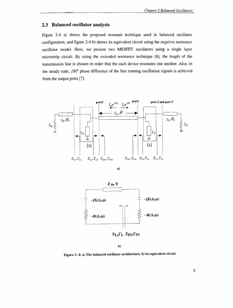
Figure 2-4 a) shows the proposed resonant technique used in balanced oscillator
configuration, and figure 2-4 b) shows its equivalent circuit using the negative resistance
oscillator model. Here, we present two MESFET oscillators using a single layer
microstrip circuit. By using the extended resonance technique [6], the length of the
transmission line is chosen in order that the each device resonates one another. Also, in
the steady state, 1800 phase difference of the free running oscillation signals is achieved
from the output ports [7].
portl' port 2 and port 2'
Zo,e
Zo Zo
[s] [s]
a)
1 -.iX(A,ro) 1
-jX(A,ro)
-R(A,ro) -R(A,ro}
b)
Figure 2- 4: a) The balanced oscillator architecture, b) its equivalent circuit
8

Chapter 2 Balanced Oscillators
An easier way to understand the oscillation condition is to view the balanced oscillator as
an impedance on the Smith chart and this has been studied by K.S.Ang [7]. A two-port
negative resistance approach [4] is used to generate the input impedance, ZlN] or ZlN2.
Either ZLl or ZLZ represents the load impedance. The input impedance and the load
impedance in this case are voltage dependent and frequency dependent. By using a
transmission line, the input impedance of the first device, ZlNlA, OJ), is transformed to the
load impedance ZL2(A, OJ), seen by looking at the other end of the transmission line. It is
conjugate. The input impedance and the load impedance can be expressed as:
(2.5)
ZLl(A,OJ) = ZL2(A,OJ) = -R + jX (2.6)
The impedance transformation is clearly depicted on the Smith chart as shown in figure
2-5. In addition, in the steady state the oscillation condition becomes:
ZINl (A,OJ) + ZLI (A, OJ) = 0 or vice versa (2.7)
Figure 2- 5: The Smith chart shows load and input impedance for the extended resonance technique
9

Chapter 2 Balanced Oscillators
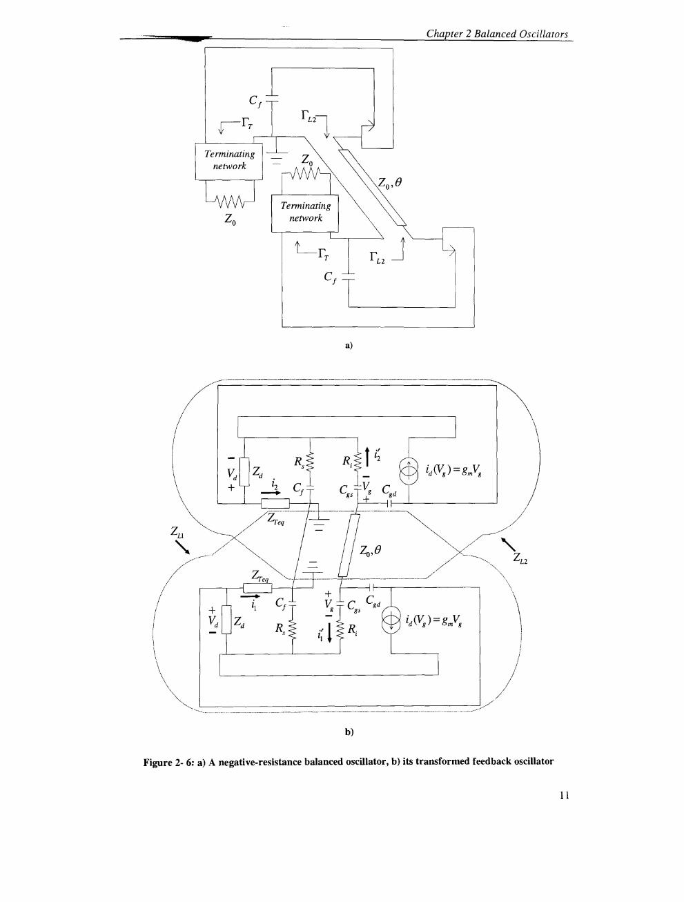
Also, the balanced oscillator can be analysed with the feedback model. Figure 2-6 a) and
b) show the balanced oscillator viewed as the feedback model [10] and its equivalent
circuit. Here, the active device functions as the amplifier, which is a voltage-controlled
current source. The output current is fed back to the resonant network where the negative
resistance model is charaterised as presented in figure 2-4. In this case, the resonant
network consists of the linear and nonlinear components. It is clearly shown that the two
active devices in the balanced configuration resonate with each other.
10
a
Terminating network
~r T
Chapter 2 Balanced Oscillators
a)
b)
Figure 2- 6: a) A negative-resistance balanced oscillator, b) its transformed feedback oscillator
11

Chapter 2 Balanced Oscillators
Next, we consider the negative resistance looking into the gate and source terminals.
Figure 2-7 b) shows an equivalent circuit of the negative-resistance technique used in the
oscillator. An external capacitance, Cf, is used to connect at the source of the field effect
transistor (PET). To evaluate the value of the resistance looking at the gate-source
terminal, it is assumed that the impedance of the gate-drain capacitance, Cgd, is much less
than that of the gate-source capacitance, cgs , so at high frequency the gate-drain
capacitance is negligible. In other words, it is assumed that no current passes through this
capacitance at high frequency.
a)
Gate Rg Cgd Rd Drain
NW +1
I V Cgs i d (Vg) = g m Vg + g
Cds Vd g ds
iii Ri
r v. I
Zin Rs
Cf T Source Source
b)
Figure 2- 7: An equivalent circuit of the negative-resistance technique
12

Chapter 2 Balanced Oscillators
From the equivalent circuit, we obtain
(2.8)
(2.9)
(2.10)
(2.11)
Where
dId I g m = -- V g = v go and S = j OJ dVg
From equation (2.8) to (2.11), we get
(2.12)
Finally, the impedance looking at the gate-source terminal can be expressed as follow:
V· Z. =R +_1 In g
1i
Vg +SCgsRiVg +-l-vg(gm + scgJ+Rsvg(gm +scgJ = R + _______ s_c..::....f ___________ _
g
(2.13)
13

- Chapter 2 Balanced Oscillators
Since
Z. = Re[Z. ]+ Im[Z. ] In In In
(2.14)
(2.15)
Equation (2.14) and (2.15) show the real and imaginary parts of the impedance looking at
the gate-source terminal of the active device, respectively.
Due to the nonlinearities in the MESFET equivalent circuit, the eN or QN characteristic
of an element has been examined [9]. A nonlinear capacitance can be presented as the
nonlinear dependence of charge on voltage: -
(2.16)
Where Qc is the capacitor charge. By usmg a Taylor senes, the charge function is
expanded. Then, subtracting the dc component of the charge, the small-signal component
of charge is:
(2.17)
14

Chapter 2 Balanced Oscillators
The small-signal current is the time derivative of the charge and is given as
. dq l=-
dt
(2.18)
For simplicity, the small-signal current can be expressed as
(2.19)
The MESFET's channel current represents the controlled current, id, and the gate-drain
conductance, gds. The controlled current is gate voltage and drain voltage dependent;
therefore, a two-dimensional Taylor series is used to expand the function. Then the dc
current component is subtracted from the function and the controlled current is given as
follows:
. af af 1 (a 2 f 2 a 2 f a 2 f 2 J l =-v +--v +- --v +2 vv +--v d av 1 av 2 2 av2 1 avav 1 2 av2 2
1 2 1 1 2 2
(2.20)
where v1 and v
2 are the small excitation voltages. V1•0 V2•0 are the bias point of Viand
Since function f is represented by I d (Vg , Vd ) , where the capital letters represent the large
signal voltages and currents while the lower letters represent incremental ones. It is
assumed that the magnitude of any product between V1 and V2 is small, so it is negligible.
Then, we obtain
15

Chapter 2 Balanced Oscillators
(2.21)
For the simplicity, we can express this as follows:
(2.22)
Where g m and g d are the transconductance and the drain conductance.
From the equivalent circuit, we obtain:
(2.23)
(2.24)
(2.25)
Substituting equation (2.23), (2.24) and (2.25) into equation (2.9), we get
16

Chapter 2 Balanced Oscillators
_ (() 2 3 )dVg Vi - Vg + Ri Cgs1 Vg + Cgs2 (Vg )Vg + Cgs3 (Vg )Vg + CgS4 (Vg )Vg dt
[( 2 3 2 3 J + R g ml V g + g m2 V g + g m3 V g + g dl V d + g d2 V d + g d3 V d) +
s ( () 2 3 )dV g C gsl Vg + C gs2 (Vg )V g + C gs3 (Vg )V g + C gs4 (Vg )V g ---:it
(2.26)
Finally, the impedance looking at the gate-source terminal can be expressed as follow:
+ Vg
( () 2 3 )dV g
C gsl Vg + C gs2 (Vg )V g + C gs3 (Vg )V g + C gs4 (Vg )V g -dt
( () 2 3 )dV g
C gsl Vg + C gs2 (Vg )V g + C gs3 (Vg )V g + C gs4 (Vg )V g dt
( () 2 3 )dV g
C gsl Vg + C gs2 (Vg )V g + C gs3 (Vg )V g + C gs4 (Vg )V g dt
(2.27)
17

Chapter 2 Balanced Oscillators
Comparing equation (2.27) to (2.13), the real and imaginary parts of the input impedance
looking into the gate and source terminals are expressed as:
and
1 Im[ZJ=-SCI
+
( () 2 3) dv g C gsl Vg + C gs2 (Vg )V g + C gs3 (Vg )V g + C gs4 (Vg )V g ----;Jt
( () 2 3 )dV g
C gsl Vg + C gs2 (Vg )V g + C gs3 (Vg )V g + C gs4 (Vg )V g ----;Jt
( () 2 3 )dV g
C gsl Vg + C gs2 (Vg )V g + C gs3 (Vg )V g + C gs4 (Vg )V g -dt
(2.28)
(2.29)
The value of the resistance is very dependent upon the values of transconductance, gm,
gate-source capacitance, cgs, and external capacitance, Cf. The transconductance and gate
source capacitance are nonlinear elements and their values also relies on the biasing. In
order to get the negative resistance by this technique; therefore, the external capacitance
and dc biasing must be considered carefully.
Now, the phase difference between the outputs of the balanced oscillator is determined.
The use of the z parameters [4], [8] of the transmission line is considered. Figure 2-8
illustrates the block diagram of the balanced oscillator.
18

Two-port
Negative
Resistance :::J
f---I-+----
Z _ parameters _ of _ the
transmissi on _line, Zo,f)
Chapter 2 Balanced Oscillators
Two-port
Negative
Resistance
Figure 2- 8: The block diagram of the balanced oscillator
By using the Kirchhoff's law, we get
(2.30)
Thus, equation (2.30) can be rewritten as
(2.31)
(2.32)
Where Zll, Z12, Z21 and Z22 are z-parameters of the transmission line connected between the
two active devices. The values of these parameters are Zl1 = Z22 = -j Zo cot(), Z12 = Z21 = -j Zo csc(), and IlJl=lhl=I. Multiplying by lie jeJ in equations (2.31) and (2.32). Then
equations (2.31) and (2.32) become:
_ Z j(B2-BI) = Z j(B2-BI) + Z IN2e lie 12
(2.33)
Z - Z j(B2-BI) Z INI - 21 e + 22
(2.34)
19

Chapter 2 Balanced Oscillators
Due to the symmetrical configuration, the value of ZlNI is equal to value of ZlN2. If one
subtracts equation (2.34) from equation (2.33) and then substituting the values of the z
parameters, we obtain:
( Z ·Z t8 ·Z 8) }(82-8l) Z ·Z 8 . - IN2 +} 0 co -} 0 csc e = - INl +} 0 cot - }Zo csc 8
(2.35)
e}(82-81) = 1 (2.36)
82 = 81 or 81 ± 2n7Z" (2.37)
where e}(82-81) = cos(82 - 81) + j sin(82 - 81) and n = 1, 2, ... , n
With the directions of the two currents as depicted in figure 2-8, the equation (2.37)
shows that 82 is equal to either 810r 81 ± 2n7Z". It can be described that no matter what
the value of 81 is, the value of 82 is equal to either 810r 81 ± 2n7Z". Thus, the net
direction of the two currents flowing through the transmission line still maintains anti
phase. It is clearly seen that under the steady state the phases of the currents in this circuit
as shown in figure 2-8 agree with the analysis.
However, the characteristic impedance of the transmission line could not be equal to 20,
50 ohm. Zc denotes the characteristic impedance of the transmission line, which is not
equal to Zoo The z parameters of the transmission line become Zll = Z22 = -j Zc cote, Z\2 = Z21 = -j Zc csc8, where the angle 8 is the electrical length of the transmission line. Then,
the equation (2.35) is rewritten as
( Z ·Z 8·Z 8) }(82-8l) - Z ·Z t 8·Z 8 - IN2 +} c cot -} c csc e - - INI +} c co -} c csc (2.38)
By comparing equation (2.38) to equation (2.35) we can see that the current directions are
out of phase no matter what the characteristic impedance of the transmission line is.
To find the required electrical length of the transmission line such that the oscillation
conditions for the balanced oscillator are satisfied, a different plane parameter [4] is used.
20

Chapter 2 Balanced Oscillators
It is assumed that the characteristic impedance of the transmission line is Zo and the angle
e is the electrical length of the transmission line between port 1 and port 1'. The
scattering matrix at the reference planes at port 1 and port 2 is expressed as:
(2.39)
Assuming travelling waves on a loss-less transmission line, the scattering matrix at the
reference plane at port 1 'and port 2' is written as:
S e-j8
] 12
S22
(2.40)
To analyse the electrical length of the transmission line connected between the two active
devices, the oscillation condition is considered. A convenient technique to present and
analyse the oscillation condition is to use the knowledge of the signal flow graph. The
use of Mason's rule [4]-[8] can analyse the signal flow graph of the balanced oscillator as
shown in Figure 2-9.
a' 1
h' 1
h' 2
I a' S12 2
Figure 2- 9: The signal flow graph of the balanced oscillator
21

Chapter 2 Balanced Oscillators
The input and load coefficients are given:
(2.41)
(2.42)
Since rn = rT2 = rT • We assume that the characteristic impedance of the transmission
line connecting between the drain of the active device and the load, 20, is equal to Zoo
Then the value of rT is as shown below:
r. - 0 T-(2.43)
For the balanced oscillator the oscillation condition must satisfy equation (2.5) and (2.6),
and we obtain:
(2.44)
Where IlN2 = IrlN21LIIN2 and r L2 = IIIN21L - r 1N2 · Substituting the value of IlN2 and
r L2 ' the equation (2.44) then becomes:
1 12 j(2LSll-2B)_1 21
Sl1 e - Sl1 (2.45)
2Lsl1
- 28 = +2N1l, where N = 0,1,2, ... (2.46)
22

Chapter 2 Balanced Oscillators
Thus, the electrical length of the transmission line is calculated as given as:
e = LS ll + 1l (radian) , where LSll is the angle of Sll (2.47)
Due to the balanced structure, the oscillation condition of the other side of the oscillator
can be analysed in the same fashion as described above. The electrical length of the
transmission line connected between the two active devices is equal to 1l + Ls 11 radians,
but the transmission line, in general, has loss due to finite metal conductivity and
dielectric tan J. The actual electrical length might not necessarily be the same as the
length given by equation (2.47). In order to consider an accurate value for the length of
the transmission line, the loss due to the finite conductivity and the dielectric material has
to be determined.
Using the Infineon CFY30 GaAs MESFET as an active device and FR4 as a substrate,
series feedback is used at the source in order to achieve the negative input impedance.
The input and load coefficients are given in Table 2-1. Table 2-2 shows an example of the
electrical length of the transmission line from simulation and calculation corresponding to
various different frequencies. The simulation results confirm the accuracy of the analysis
shown in equation (2.47).
Frequency (GHz) rIN rL
1.8 1.018L-35.861 ° 1.018L35.861 °
1.9 1.042L-42.561 ° 1.042L42.561 °
2.0 1.070L-49.077° 1.070L49.077°
2.1 1.100L-55.451 ° 1.100L55.451 °
2.2 1.134L-61.722° 1.134L61.722°
Table 2- 1: The input and load coefficients with respect to different frequencies

Chapter 2 Balanced Oscillators
Length of the Length of the
Frequency (GHz) transmission line by transmission line by
simulation (J.Lm) calculation (J.Lm)
1.8 36160 36215
1.9 32645 32702
2.0 29500 29583
2.1 26740 26792
2.2 24230 24277
Table 2- 2: The length of the transmission line by simulation and calculation for different frequencies
2.4 A self-oscillating balanced mixer
As a practical application of the balanced oscillator a balanced self-oscillating mixer is
now presented. A mixer is an important block in communication systems. The balanced
mixer has many advantages over the single-ended mixer such as the RF-LO isolation [5],
[9]. There have been many studies on balanced mixers and self-oscillating mixers [12]
[19]. The balanced self-oscillating mixer has inherent oscillating signals and functions as
the mixer at the same time by the non-linear mechanisms in the device. The other
advantage of the self-oscillating mixer is that the RF signal is down converted to the IF
signal without a balun or external oscillator signals.
Typically, the singly balanced mixer requires an external LO signal with the external
balun or 180-degree hybrid. There are many important parameters in the balanced mixer.
The design considerations for the balanced mixer are examined. Similar to the balanced
mixer, the self-oscillating mixer requires the same performances. In this case, the biasing
point is carefully considered in order to obtain the conversion gain.
24

Chapter 2 Balanced Oscillators
The design of the self-oscillating mixer is concerned with the inherent oscillating and
mixing mechanism. The balanced oscillator configuration and the gate mixer topologies
are used to accomplish the purpose. Furthermore, this design topology is also expected to
maintain the balanced properties under the mixing operation by employing the
symmetrical configuration. The return loss at the RF port has been taken into account so
that the maximum RF signal can be taken into the circuit.
Additionally, the phase and amplitude of the IF signals at the drains of PETs also have
been investigated. Then, the IF signal was subtracted by using an external balun. The
measured results demonstrate the conversion gain as a function of the RF power levels
with different biasing points. The advantages of this technique are the small size of the
circuit, reduced power consumption and simple design.
2.4.1 Design considerations for a balanced mixer
The basic building block of a singly balanced PET mixer is typically composed of a 180-
degree hybrid for the RF and LO inputs, PET mixers and an other 180-degree hybrid to
combine the IF signals. Figure 2-10 shows a 180-degree hybrid mixer. The RF and LO
signals are applied to the identical mixers via the hybrid. The LO signals injected to the
PETs have 180-degree phase difference whereas the RF signals are in-phase. The 180-
degree out-of -phase IF signals are subtracted by using either a balun or hybrid. The
advantage of this configuration is that it gives RF-to-LO isolation due to the use of the
hybrid.
Although the balanced mixer topology provides the two mutual isolated ports of the 180-
degree hybrid, there are the other properties to be carefully considered. First is the AM
noise-rejection properties. In an ideal balanced mixer, this property is limited by the
balance of the hybrid and the AM noise in the LO signal [5], [Ill The other is the RF-to
IF isolation. This can be achieved by using either the IF balun or hybrid, where the two
out-of-phase IF signals are subtracted.
25

Chapter 2 Balanced Oscillators
FET MIXER
~ IF RF
180-degree 180-degree HYBRID HYBRID
LO
FETMIXER
Figure 2- 10: The basic building block of a singly balanced FET mixer
A self-oscillating balanced mixer functions as both the balanced mixer and balanced
oscillator simultaneously. Similar to the typical balanced mixer, a self-oscillating
balanced mixer requires the same considerations. However, the other important
consideration for the self-oscillating mixer is that the balanced oscillator is not locked to
the injected RF signal. That means the circuit must perform as the self-oscillating mixer
rather than the injection-locked oscillator. The mixing operation can be achieved by
considering the device non-linearity. The important key controlling operation is the
device non-linearity, which has been studied in many previous works [5], [11]. The self
oscillating mixer can provide the conversion gain at a bias condition where the non
linearity is strong. The dc-bias operating point for a PET mixer is considered [13]-[15].
Furthermore, the conversion gain/loss is also dependent on the circuit topology of the
mixer [5], [11].
2.4.2 Circuit realisation
A balanced self-oscillating mixer, shown in Figure 2-11, consists of two important parts,
namely, a common-source feedback oscillator and a gate mixer. Series feedback is at the
source of the PET so that the instability for the active device is achieved. Then, the use of
the two-port negative resistance approach is applied to build the oscillator. From equation
(2.48), the circuit meets the oscillation conditions, which are generally described in many
literatures [4], [5]:
26

Chapter 2 Balanced Oscillators
Re[ZTNI (A,m)] + Re[ZLl (A,m)] < 0 or vice versa (2.48)
Im[ZTNI (A,m)] + Im[ZLl (A,m)] = 0
Balanced Oscillator
0 180 degree + degree
Gate Mixer
Figure 2- 11: A block diagram of the Balanced Self-Oscillating Mixer
To design the self-oscillating balanced mixer as illustrated in figure 2-12, each part of the
circuit is examined. Firstly, the balanced oscillator is designed. The design method as
described in section 2.3 is used. The Infineon CFY30 GaAs PETs are used as active
devices. The circuit is fabricated on FR4 substrate.
Next, the LO and RF rejection is determined. In order to eliminate the LO and RF signals
at the drains of the active devices, a low pass filter is required. This filter is designed to
function as the matching network for the oscillation condition as well as to perform as the
low pass filter for the IF signals.
Finally, the RF port is considered. The RF matching is examined in order that the
maximum RF signal can couple into the circuit. In this case, a coupled transmission line is
used. This coupled line functions as the band pass filter for the RF signal. It is connected
at the mid-point of the transmission line connected between the gates so that the circuit
can maintain the balanced configuration during oscillation and mixing operations. The
27

Chapter 2 Balanced Oscillators
return loss of the RF port is shown in figure 2-13. This is the simulated result when 50-
ohm loads are used to terminate the output ports of the circuit.
Z --R-jX V I~ GS..=.
~ -
IF -IF
RF
Figure 2- 12: A circuit diagram of the Balanced Self-Oscillating Mixer
0.0 (
-5.0 , , '
- - - - - - - -- - ---- - - - ---~ - - - ---- - ------ - - -- -;-- ----- - ----- - ------ -- ~ ---- -----------------
I 1 1
, ' ' --------------------1---------------- ----:--------------------1---------------------, , ' , , ' , ' ' , , ' , ' ' , ' ' : : : , , ' , ' ' , ' , ' , ' ' --------------------1---------------- ----:--------------------1------------------ ---, : '
-10.0
-15.0
-20.0 0.0 4.0
Frequency 1.0 GHzlDIV
Figure 2- 13: Simulated performance of return loss at RF
28

Chapter 2 Balanced Oscillators
2.4.3 Results and discussion
The self-oscillating balanced mixer was built and tested. The DC bias was provided by
bias-tees. The biasing point was considered in order to get the significant effect on the
mixing process due to the non-linearity of the devices, where a mixing operating point
close to class B is preferred [13]-[15]. This could enhance the conversion gain. The
circuit was first terminated at the RF port with 50-ohm load. The circuit then provided
1.85-GHz oscillating frequency with -5.2-dBm amplitude, which was corresponding to
the designed oscillation frequency, and the fact that the LO output is suppressed due to
the low-pass filter at the output of the circuit. The leakage of oscillating signal at the RF
port was measured by terminating with 50-ohm loads at the two outputs. The value of the
leakage signal was -20 dBm.
Next, the waveform of the IF signal from the drains of the devices was investigated. A
1.78-GHz RF signal was fed into the RF port. Figure 2-14 illustrates the waveform of the
IF signals. It is noticed that the amplitude and phase of the IF signals from the drains are
equal and 180-degree out-of phase.
10
20
;; 30 e
'-" QI "0 0 = ..... '8 ell -10 = ~
-20
-30
120.0mV 220.0mV
'I . :1
1
r
" '. ~ ..... '::: .. -
; ....... Ii .. . I:
.l-O.OOs S.OOns/
,.. ,
· . , ! .. , ~" ....... : . " . · . · .
1.. ' ..... ,' . A .". ,!,~".,,, i." i,.,.> .... ,-,.,
~
t
Vp-p(I)=8S.62mV Vp-p(2)=83.12mV Freq(2)=70.0SMHz
Time(ns) S.OOns/
Figure 2- 14: The anti-phase IF signals at the two outputs
29

Chapter 2 Balanced Oscillators
The conversion gain of the balanced self-oscillating mixer was observed. Figure 2-15
shows the experimental set-up. In this case an external IF balun was used to subtract the
two IF signals in order to obtain the conversion gain for the down-conversion. The
conversion gain as a function of the RF input power levels for difference biasing points
was measured. Figure 2-16 indicates the measured conversion gain. The mixer conversion
gain is flat up to an RF power level of -15 dBm. The maximum conversion gain is
approximately 2.5dB.
A Balanced IF signal signal .... IF Spectrum RF
~
~ "'0 '-" ~ ..... ro 01)
~ 0 ..... CI.l
""" ~ ;> ~ 0
U
...,... .... Self-Oscillating
... ..... ....... analyser .... Balun
Mixer -...
Figure 2- 15: Measurement set-up
5
.J.. * ~ 0
-5
-10
0" ~u v U V~ ~ ~ " A. A
~~ \ "
\~ ~ (r~ i * ~
\ \
-15
-20
-25
-30
-35
\
\ \\ \ ~
-*- Vds = O.9V , Vgs = -O.05V 1\1 -e- Vds = 1.0V ,Vgs = o.ov \\ ---*-- V ds = 1.2V ,v gs = o.ov
\ -40
-30 -28 -26 -24 -22 -20 -18 -16 -14 -12 -1 0
Input power (dBm)
Figure 2- 16: Conversion gain vs. input power
30

Chapter 2 Balanced Oscillators
As seen from the experimental results, this designed circuit topology gIves many
advantages. One of these is the good RF-to-LO isolation due to the small amount of the
LO leakage power level at the RF port, but the RF matching is narrow band. In addition,
the designed circuit is simple: using the balanced configuration to maintain the balanced
properties of the balanced mixer. From this it can be stated that the directions of the RF
signal looking at the two gates of the PETs are in-phase, mixing with the ISO-degree LO
signals, since the IF signals obtained from the drains are ISO-degree out of phase. The
other point is that the circuit consumes less power and the circuit size is smaller compared
to the typical balanced mixer since the external oscillator and external balun for the lS0-
degree for the LO input are not required.
2.5 Conclusion
This chapter has introduced the balanced oscillator technique. To do this, the oscillation
condition was considered. This condition can both be viewed as the simple negative
feedback oscillator and negative resistance oscillator models. In microwave design, the
two-port negative resistance is used to ensure the instability of the device. Next, the
negative-resistance approach is described. By utilising the external capacitance
connecting at the source of PET, the negative resistance is produced. Its value is
dependent on nonlinear and linear components.
The balanced oscillator can be viewed as the feedback model, where the active device
behaves as an amplifier generating the harmonic signals and the feedback network part
can be considered for the oscillation condition. This model is explained more in next
chapter. Additionally, some analyses have been presented in order to demonstrate the
balanced properties of the circuit where the two active devices are identical and to
calculate the length of the transmission line used in the balanced oscillator design
topology. The simulated electrical length well agrees with the calculated one.
A self-oscillating balanced mixer was introduced to demonstrate the balanced oscillator in
a practical example. The biasing point in the self-oscillating mixer circuit was determined
since it ensures the mixing operation. As the results of the experiment, the self-oscillating
balanced mixer provided a 2.S-dB maximum conversion gain. The balanced properties
31

Chapter 2 Balanced Oscillators
were investigated and the results agree with the analysis. Furthermore, the LO signal
power level at the RF port was -20 dBm, which shows the good RF-to-LO isolation.
32

Chapter 3 Injection-locked Balanced Oscillators
Chapter 3
3 Injection-Locked Balanced Oscillators
3.1 Introduction
Local oscillator phase noise is a key performance parameter in a communication system,
since, for example, it effects the rejection of adjacent channel interference (AeI) and the
ability to detect weak signals, called the receiver sensitivity. Therefore the low phase
noise oscillator signal is needed in the next generation of millimetre wave communication
system. A technique popularly used to stabilise the free-running frequency is the
injection-locked oscillator. This also introduces an improvement of the phase noise in the
oscillator. The prospect of using the synchronous oscillator to a lock signal at the same
frequency (free-running frequency) or a higher frequency (harmonic frequency) have
been widely studied in the literature [20]-[39]. The fundamental and sub-harmonic
injection-locked technique has been also studied as a particular technique for optical
synchronisation of the remote local oscillator in microwave and millimetre-wave
applications [23]-[24]. Recently, an injection-locked push-pull or balanced oscillator was
proposed and applied to a spatial power combining array antenna [25]. Though the
structure proposed in [26] can be applied with external fundamental and sub-harmonic
injection signals, its main disadvantage is a large circuit area due to a use of a
transmission line to achieve 1800 phase difference outputs.
In this chapter, the explanation of phase noise theory is introduced. Leeson's model [47]
is generally used to describe phase noise. This reveals the important parameters which
effect the phase noise performance in oscillator. Therefore, these parameters, such as the
Q factor of the tank circuit, are determined for the oscillator design. Also, the injection
locked balanced oscillator is analysed in section 3.3. By characterising the balanced
oscillator with the negative-resistance and feedback models, the locking phenomenon is
33

Chapter 3 Injection-locked Balanced Oscillators
determined. Kurokawa's theory [21]-[22] is used to explain the locking range and phase
noise improvement. We extend Kurokawa's work by using the feedback model, which
has a feedback network characterised as a negative-resistance approach.
For more understanding about the injection-locked oscillator technique, we propose a
novel structure for a fundamental and sub-harmonic injection-locked balanced oscillator
(SILBO). The injection-locked balanced oscillator design approach is based on the
extended resonance technique [6]-[7], which is described in Section 3.4. Sections 3.5 and
3.6 describe the implementation and measurement results, respectively. The stabilised
injection-locked oscillating signal and the locking range with respect to the level of the
injection power are investigated. It also shows the balanced amplitUde and phase
difference between the two outputs of the fundamental and sub-harmonic injection-locked
oscillators under the locking state. These experiments were set-up in order to verify the
amplitude and phase output properties of the balanced oscillator. The advantage of the
injection-locked balanced oscillator technique is that it is simple to design and the circuit
consumes low power. In addition, the circuit size is relatively small because a circulator
and balun at the injection port and input/output ports, respectively, are not required.
3.2 Phase noise theory
An oscillator generates a periodic signal from its own circuit noise [40]. The oscillation
may be started by the noise generator [41]. It induces an exponentially growing
oscillation until the stable oscillation is achieved by some limiting mechanism. This
mechanism limiting the growing signal has been observed by many researchers [40]-[42].
The magnitude grows until the system reaches the sufficiently positive nonlinear
resistance [42]. Then, the oscillating signal becomes a periodic signal with an operating
point at which the positive and the negative resistances cancel, as described in chapter 2.
The electronic nOIse sources that provide the nOIse III any oscillator system can be
categorised into two main groups. The first group is the so-called intrinsic noise sources
and it consists of thermal, shot, and flicker noise. These noise sources arise from random
fluctuations within the physical systems [44]. The other is interference, which is
34

Chapter 3 Injection-locked Balanced Oscillators
determined as the undesirable effect of noise from outside. The supply nOIse IS an
example of the latter group.
Even for a steady-state oscillation, noise is still present. Noise affects the oscillating
signal, causing fluctuations in the operating frequency. It appears as sidebands of the
signal. This noise is separated into AM and PM components. For the amplitude
modulation mechanism, the noise voltage in the spectrum can be added in a power or
root-sum-square basis, so the AM components can represented as a pair of symmetrical
sidebands. The phase deviation is defined as the PM modulation index l1¢max. The
frequency spectrum for the two sidebands is theoretically presented above and below the
carrier frequency, but a pair of these sidebands is anti-symmetrical. Therefore, the noise
voltage due to the AM and PM components is represented as sidebands of the carrier as
shown in figure 3-1. The noise voltage at the lower noise sideband can be cancelled out.
\b~age \b~age \b~age
input input input
Vc Vc Vc
L L 1 \h1
I I VnJ2
\ VnJ2 + VnJ2
> Rl.dian I I > :~~~ncy
Rl.dian frequency
" 1/
(J) i frequency i (J) i c c
((J) +(J) ) ((J) -(J) ) ((J) +(J) ) -VnJ2 c n c n c n
i ((J) +(J) ) c n
((J) -(J) ) c n
Rv1
Figure 3- 1: AM and FM components
For a better understanding, I.G.Ondria [45] has shown that the vector diagram of a carrier
simultaneously phase and amplitude modulated by the nth noise voltage interference as
depicted in figure 3-2. The noise component is located at OJn above the carrier. It is
assumed that Vn «V" where Vn and V, are defined as the noise and carrier voltages,
respectively. The vector diagram shows that a carrier at radian frequency OJe has been
35

Chapter 3 Injection-locked Balanced Oscillators
amplitude and phase modulated at the radian frequency (j)n. From this, the instantaneous
resultant carrier voltage Vet) can be expressed as
Where en is an arbitrary phase angle.
carner
voltage V c
4
3i
CD c
V (rrn s) = nth noise n
voltage
2
instantaneous resultant /" carner voltage
~r ~'" = instantaneous
-- ~ - n phase deviation
(3.1)
Figure 3- 2: Vector diagram of a carrier simultaneously phase and amplitude modulated by the nth
noise voltage interference
For AM and PM noise in a microwave oscillator, all noise components are found by
summing the magnitude square of the components [46]. Figure 3-3 illustrates the signal
spectrum in frequency domain. If we assume that the AM noise is practically very low in
comparison with the PM noise, the PM noise components are defined as phase noise.
Phase noise is the standard deviation of phase fluctuation in oscillators and is also
quantified by its short-term frequency stability. It is defined as the ratio of the single
sideband (SSB) power, in aI-Hz bandwidth fm Hz away from the carrier, to the total
signal power [47].
36

Chapter 3 Injection-locked Balanced Oscillators
Ps
IPssb/Psl
fo
Figure 3- 3: Spectrum of source in frequency domain
To broaden the understanding of the phase noise in oscillators, an oscillator model is
introduced. By using Leeson's model as the simplest possible model of the oscillator
circuit [47]-[49], an oscillator is viewed as a feedback system. The noise sources are
considered as an input, shown in figure 3-4. The phase noise can be modelled as a noise
free amplifier with phase modulation at the input. The transfer function of the modulated
RF signal passing through the bandpass filter equals the transfer function of the
modulating signal passing through an equivalent lowpass filter [47]. The transfer
function in this model can be explained as follows:
Phase modulator
>--~------i Reso nator
Noise-free
Amplifier
Figure 3- 4: Leeson's model
37

Chapter 3 Injection-locked Balanced Oscillators
As mentioned in figure 2-1 in Chapter 2, the oscillator consists of the amplifier and the
resonator. The noise figure is determined as the noise added to an amplifier and it can be
defined as
F = (S I N)in
(S I N)out (3.2)
Where F is the noise figure, (S I N)in and (S I N)out are the signal-to-noise ratio at the
input and output of the amplifier, N in and N out are the noise power at the input and output
of the amplifier.
The noise figure is determined as the input phase noise in a I-Hz bandwidth at frequency
offo+fm from the carrier, causing the phase deviation. This phase deviation is given by
v ~e = n,rms
peak Vpavail,rms
FkT (3.3)
In rms terms, we get
~e =_1_ FkT rms Ji P
avail
(3.4)
Where Vn,rms and Ppavail,rms are represent an equivalent available noise voltage due to the
noise figure of the amplifier and the available rms signal power. G, T and K represent the
gain of the amplifier, temperature in Kelvin, and the Boltzmann's constant equal to1.38x
10-23 W.S/oK, respectively.
With a random noise phase relation to the noise signal atfo+fm. the same phase fluctuation
of the signal exists at the frequency of fo-fm from the carrier. If the values of ~e rms are
added, then the total phase deviation is:
38

Chapter 3 Injection-locked Balanced Oscillators
i18 = rrns,total (3,5)
Transforming into the spectral density:
s . = i18 2 = FkT 8m rrns p
avail
(3.6)
Also, a flicker noise or lIf noise component is described by the comer frequency fe, which
is low-frequency device noise in the transistors. The signal purity can be degraded by the
flicker noise at the frequency close to the carrier due to phase modulation. From this, the
spectral phase noise becomes
(3.7)
As mentioned above the transfer function of a modulating signal in Leeson's model can
be characterised as the transfer function of the modulating signal passing through an
equivalent lowpass. The tank circuit can be viewed as a bandpass resonance resulting in
the lowpass transfer function given by:-
(3.8)
Where mm andmo are the offset frequency and carrier frequency in radians, respectively,
The QL represents the loaded Q factor. Equation (3.8) shows that the phase noise is
transformed through the resonator up to the half of bandwidth. The resonator attenuates
the passing phase noise with 6 dB per octave when the modulation rate increases further
[47]-[ 49]. Then the closed loop response of the phase feedback loop is determined by
1 i18 (m) = i18. (m )
out m 1 '(2Q / ) m m + ] LOJm OJo
(3,9)
39

Chapter 3 Injection-locked Balanced Oscillators
The power transfer function is transformed into the phase spectral density as expressed as:
(3.10)
The phase noise at the output of the amplifier with the RF modulating input is given by:
(3.11)
Substituting equation (3.7) into (3.11), then the phase noise becomes:
(3.12)
Equation (3.12) shows the phase noise in the oscillator due to phase modulation and noise
source in the oscillation system. Not only the noise figure, F, and the lIf noise, which are
inherent in the active device, are the main important parameters to determine phase noise,
but the loaded Q factor due to the tank circuit is also crucial. Hence, in order to reduce
phase noise in the oscillator these parameters are considered. For example, the selected
active device should provide a small value of the noise figure. Also, the tank circuit or
resonator should be selected in order to maintain the maximum loaded Q value.
3.3 Injection-locked oscillator theory
There has been great interest in the injection locked oscillator technique [20]-[39]. This
technique is used to stabilise the oscillating signal by injecting a stable reference signal
into the free-running oscillator. Alder [20] described the case of synchronisation where
the external signal is impressed on an oscillator. When the external signal is modulated
with the free-running signal, the oscillator signal contains strong harmonics
/).OJ = OJo - OJi
if the oscillator is almost locked [20]. His work also showed that the speed
40

Chapter 3 Injection-locked Balanced Oscillators
of the locking process is proportional to the ratio of the injecting voltage and to the
oscillator voltage and the bandwidth of the tuned circuit. Later, the noise improvement of
the oscillator by the synchronisation approach was analysed by Kurokawa [21]-[22]. The
negative resistance oscillator model was used and a graphical approach in terms of device
and circuit impedance loci was employed to describe the injection phenomenon. A
stability criterion was developed. The intersection of the two impedance loci depending
on the amplitude and frequency change indicated a steady-state operating point. With a
small injecting signal whose frequency is close to the free-running frequency, the
relationship between the injection vector, impedance locus and device line are considered.
The locking condition is dependent on the ratio of the magnitude of the injection signal
and the magnitude of the free-running frequency signal. He also explained the noise
reduction in a synchronised microwave oscillator. The FM noise can be greatly improved.
However, the PM noise improvement depends on the injection signal purity.
However, both Adler's and Kurokawa 's works can only explain the injection locking
phenomenon in the case when the injection frequency is close to the free-running
frequency. Other works associated with the injection locked oscillator have been reported,
and many different methods of injection locking have been studied. There are many
injection-locked oscillator studies using sub-harmonic and super-harmonic injection [22]
[39]. The latter case is of less importance in a microwave circuit system since it is not
easy to create the stabilised external signal at high frequency in practice.
In order to examine the injection-locked oscillator technique for fundamental and
subharmonic modes, an oscillator model is needed. Figure 3-5 a) shows the equivalent
balanced oscillator circuit where the injection signal is applied at the centre of the
transmission line. From equation (2.13) and (2.27), the simplest equivalent oscillator on
either left- or right-hand side of the balanced oscillator can be modelled as shown in
figure 3-5 b). Under the free- running oscillation condition, e(t) is equal to zero.
Considering a current loop as shown in figure 3-5 c), the equation for the current i is
expressed as:
41

Chapter 3 Injection-locked Balanced Oscillators
L di +(-R-R)i+-1 Jidt+~Jidt=O
dt C1 C
woL and Q --'--
loaded - R + R (3.13)
B • 1
- R(A,w)
ZIN\////
e(t)
[ Injection
: Zo,8 A
i 1------<1 ·---~l C(A,wJ
- R(A,w)
a)
.....
Z Vd d
+
b)
(3.14)
.+2

Chapter 3 Injection-locked Balanced Oscillators
e(t)
1 i(t)
- R(A,m)
c)
Figure 3- 5: a) A equivalent circuit for the oscillator, b) equivalent circuit characterised in both
negative and feedback models and c) equivalent oscillator on right-hand side of the balanced
oscillator
By using Kurokawa's theory [21], neglecting harmonic terms, then equation (3.14) can be
written as:
(3.15)
Where m = = --, C = ,and then: ~CI +C fzE CIC LeI C LC x x CI + C
di(t) (d9 J dA (t) --=-AI(t) m+-I sin(ox+91(t))+ I cos(ux+91(t)) dt dt dt
(3.16)
fi(t)dt = (AI (t) _ Al (t) d91 JSin(OX + 91 (t)) + ~ dAI (t) cos(ux + 91 (t)) m m 2 dt m dt
(3.17)
Substituting equation (3.15) to (3.17) into equation (3.13), then multiplying by either
cos(mt + 9(t)l) or sin(mt + 9(1)1) and integrating with respect t from t - To to t, where To

Chapter 3 Injection-locked Balanced Oscillators
is a period of the free-running oscillation, Kurokawa showed the resultant equation is
expressed as:
(3.18)
( 1 JdA - 2 t L+-2 - --+(Rj-R)A=- fe(t)cos(OX+¢)dt
m ex dt ATa t-To
(3.19)
Where R is an average resistance over one cycle and is a function of A. The value of it is
given by:
2 I
R = -- f RA cos 2 (OJ{ + ¢ )dt ATo I-To
(3.20)
Now considering the synchronised oscillator mechanism, Kurokawa explained the
injection-locked phenomenon for the fundamental injecting signal, where the injection
frequency is close to the free-running frequency. He assumed that the external injecting
signal is e(t) = ao cosmJ, where ao is small. When the oscillator is synchronised, the
oscillating frequency must be ms. The right-hand side of equation (3.18) is replaced by
~ sin ¢. For the steady state, d¢ = O. Then the difference frequency between the Ao ~
synchronising and free-running frequency is given as
-a a !::..mo = __ 0_ sin ¢o or I!::..mo I ::; __ 0 - sin ¢o
2LAa 2LAa (3.21)
To use Kurokawa's theory [21] in the subharmonically injection-locked case, the
feedback oscillator is used. The equivalent circuit characterised in both negative and

Chapter 3 Injection-locked Balanced Oscillators
feedback models is introduced in figure 3-5 b). From this, we assume that the injecting
signal is fed into the amplifier. The output current at the output of the amplifier is fed
back into the feedback network, where the negative resistance oscillator model is
characterised. The nth harmonic signal is generated. This is due to the nonlinearity in the
amplifier. As a result, e(t) is replaced by:
where mo is close to nms.
Then the right-hand side of equation (3.18) is replaced by ~ 0 sin ¢. In the locking state,
the locking range becomes:
(3.22)
For the harmonic case, an external injecting frequency is close to n times the free-running
frequency, mo :::::: ms / n . The locking range is denoted as tlmO(lIn). In the locking state, the
right-hand side of equation (3.18) is replaced by bn sin ¢, where the absolute value of Ao
bn is higher than that of ao and the absolute value of ao is higher than that of an.
Comparing the locking range between the fundamental and the harmonic injection locked
phenomena, we found that the locking range for the harmonic is higher than that for the
fundamental in which the injection signals are the same. However the locking range for
the fundamental case is higher than that for the subharmonic case. Therefore, it can be
noted that at the same injecting power level the relation of locking bandwidth for
harmonic, fundamental and subharmonical injection-locked oscillator is:
(3.23)
Where n=1,2, ...
From equation (3.21), Kurokawa described the locking range in terms of power. He
assumed that the available power of the injection signal source is denoted by Ps and the
45

Chapter 3 Injection-locked Balanced Oscillators
output of the free-running oscillator is defined by Po. The values of Ps
and Po are given
as follows:
(3.24)
P = R (~J2 = RoAg-o 0.fi 2
(3.25)
Substituting (3.24) and (3.25) into (3.21), then:
(3.25)
( !J..mo J2 < _1_ a;
- 2 2 mo Qext ~
(3.25)
mL. . Where Qext = _0 - and Ro 1S the load res1stance.
Ro
The external stabilised power is injected into the oscillator. The harmonic power
components are generated due to the nonlinearity of the active device. As a result, the
power is passed through the feedback network. Here, the injection-locked phenomenon is
considered at the feedback network, where the negative-resistance model is operative.
The locking range for the harmonic and the subharmonic locking oscillator can also
described in the power form by considering only the fundamental component of power
fed back through the feedback network.
Next, the phase nOIse degradation in the injection-locked oscillator is determined.
Leeson's equation is used to explain the phase noise. Focusing on one half of the
resonator [47], equation (3.12) can be expanded as follows:
46

Chapter 3 Injection-locked Balanced Oscillators
(3.26)
Where QL can be defined as the ratio of reactive power to total dissipated power [47]:
Q L = 27(0 We 27(0 We
P diss (total) ~n + Pres + P sig
(3.27)
Where We represents the reactive energy going between Land C and Pres is the power
dissipated in the resonator. ~n and P sig are input power and signal power, respectively.
Putting (3.27) into (3.26) gives:-
(3.28)
Then we consider the phase noise suppression factor of an injection-locked oscillator,
which is defined as the phase noise ratio between the injection-locked oscillator and the
free-running oscillator:
The phase noise suppression factor = [. (f m ) injection-locked / [. (f m ) free-running (3.29)
[ J
2
We(free-rUnning)
- We(injection-locked)
(3.30)
Where W = ~ CV 2. We transfonn the voltage fonn into the power fonn. It is assumed e 2
that the power is due to the power of the free-running oscillator and that available from
the injection signal. Then, equation (3.28) becomes:
47

Chapter 3 Injection-locked Balanced Oscillators
The phase noise suppression factor = (CIRo~ J2 C2RoP2
Where ~ = Po and P2 = Po + Ps • From equation (3.25), P2 is given as:
(3.31)
(3.32)
Substituting (3.31) into (3.32), and assuming that there is no capacitance change in the
injection-locked oscillator, then the phase noise suppression is found as follows:
The phase noise suppression factor", [1 + ( "': J Q:" J (3.33)
Equation (3.33) can be rewritten as the phase noise of the injection oscillator as shown
below:
(3.34)
As shown in equation (3.34), the phase noise suppression factor is dependent on the
locking range and the external quality factor. In the locking state, it is shown that the
nois'e far away from the carrier will be rerduced by the phase noise suppression factor.
Additionally, the degree of phase noise improvement not only relies upon the injection
frequency, which can be a harmonic, fundamental or subharrnonic frequency, but also
depends on the power level of the injection signal as described above.
48

Chapter 3 Injection-locked Balanced Oscillators
3.4 Design considerations for the injection-locked balanced oscillator
Highly stabilised oscillators with low phase noise are in high demand for many electronic
systems. The injection locking technique has been proposed [20]-[22] amongst other
techniques to provide a stable oscillation signal. An injection locked push-pull oscillator,
alternatively called an injection-locked balanced oscillator, was first proposed [26] for
spatial power combining, where the oscillators are synchronised using a single patch
resonator or antenna [25]. The circuit consists of two active devices and two 1800 phase
shifting transmission lines at both input and output of the push-pull oscillator. Those two
phase-shifting components consume a large circuit area in RFIC and MMIC realisations.
Figure 3-6 shows the proposed injection-locked balanced oscillator configuration. The
transmission line between the two devices is used such that 180-degree phase difference
free running oscillation signals are achieved from the output ports [7]. The matching
network, M2, is used to couple the injection signal power into the centre of this
transmission line. Due to the injection signal power, the non-linear devices are
perturbed. In the case of the fundamental frequency, the system will be locked to the
injecting signal. If the applied injection signal power is small compared with the free
running signals, the condition of 1800 phase difference is still maintained. It is very clear
that to apply the injection signal at the middle port requires only a matching component.
In addition, a circulator is not required at the middle port due to the balanced topology,
which allows perfect LO isolation at the injection port. Similar to the fundamental
injection-locked balanced oscillator, the sub-harmonic injection-locked oscillator
employs the same injection method, but the injection network port, M2, is considered for
the sub-harmonic frequency, (free-running frequency/2). Therefore, the injection network
port, M2, is designed corresponding to the injection frequency signal in the circuit.
49

Chapter 3 Injection-locked Balanced Oscillators
Terminating
network
Ml
12ej82
......................................... : I lej8l
t----~ ... ~ Zo,8 ~ ! +~_--.....j
M2
Z Z Z Injection Z Z Z T2 IN2 L2 L1 INl T1 signal
Terminating
network
Ml
Figure 3- 6: The proposed injection-locked balanced oscillator configuration
3.5 Circuit Realisations
The fundamental and sub-harmonic injection-locked balanced oscillators were designed
and constructed on FR4 using Infineon CFY30 GaAs FET devices. Series feedback was
used at the two sources to obtain the negative resistance and the transmission line was
connected between the gates. This causes the input impedance of one active device to be
the load impedance for the second active device, and vice versa. As described in chapter
2, in the steady state the oscillation condition is given as:
where ZLX(A, m) is the input impedance, ZIN(A, m) is the load impedance and X is 1 or 2.
Figure 3-6 shows the fundamental injection-locked balanced oscillator circuit. For the
fundamental mode, a coupled line section was used to form the injection network port,
M2. From this, the oscillation condition is taken into account and the return loss at the
injection port is also determined. The return loss should be as low as possible so that the
maximum injection power can pass into the circuit. Due to the symmetrical configuration,
the gate bias for the two active devices is common at the centre of the transmission line.
Figures 3-7 and 3-8 show the photographs of the fundamental and subharmonic injection
locked balanced oscillators. In steady state, these two circuits are expected to lock at the
injection frequency and twice injection frequency for the fundamental and sub-harmonic
injection-locked balanced oscillators, respectively.
50

Chapter 3 Injection-locked Balanced Oscillator
Injection port
Figure 3- 7: The fundamental injection-locked balanced oscillator circuit
+- Injec1ion port
Figure 3- 8: The sub-harmonic injection-locked balanced oscillator circuit
3.6 Results and discussion
3.6.1 Fundamental injection-locked balanced oscillator
Two oscillating signals were observed at zero gate bias and 2.S V drain bias. The total
power consumption is around lSmW. The LO leakage at the injection port is ob erved.

Chapter 3 Injection-locked Balanced Oscillators
The value of the LO leakage is -19dBm. This indicates that the two LO signals cancel out
each other at the mid-point of the transmission line.
Figure 3-9 shows a comparison of output spectra for two different injection power levels
compared with the free running signal from one of the output ports. The obtained free
running output signals have a power level of 3.33dBm. As the injection power level
decreases the phase noise of the output signal is increased but is still better than that of
the free-running signal. The locking range with different injection power levels is
observed. Figure 3-10 shows the measured locking range corresponding to the injection
power level. As expected, a higher injection power level provides a wider injection
locking range. The maximum locking range is 6 MHz at an injection power of -5dBm.
o -10
-- -20 e ~ "0 -30 '-"
-40
-50
-60
-70
-80
ATTEN20dB RL 10.0dBm
RBW 3.0kHz VBW 3.0kHz SWP 140ms
CENTER 1.8896500GHz RBW3.0kHz
10dBI MRK 3.33dBm 1.8896500G Hz
Free-running
VBW3.0kHz SPAN 500.0kHz SWP 140ms
Figure 3- 9: The measured free-running signal compared to the injection locking frequency signals
52

Chapter 3 Injection-locked Balanced Oscillators
6000 ..-. 5000 N
~ '-" 4000 ~ ~ = 3000 ~ ~ ~
2000 = :E2 ~ 0 1000 ~
0 -17.5 -15.0 -12.5 -10.0 -7.5 -5.0
Injection power level (dBm)
Figure 3- 10: The locking range of the fundamental injection-locked balanced oscillator as function of
the injection power level
By increasing the injection power level, the measured locking range was higher. The
locking range of the fundamental injection-locked balanced oscillator is a function of the
injection power level. These experimental results agree with Kurokawa's theory [21] as
well as with the Leeson's model [82], which is explained in the previous section.
Therefore, it is noted that Kurokawa's theory can be used for the balanced oscillator.
To investigate the phase and amplitude response between the two output ports, the test
bench is set up as follows: A -14 dBm external signal is obtained from an HP8510C
network analyser system and fed into the injection locking port of the balanced oscillator.
The first output port is connected to the second port of the network analyzer via a 6-dB
attenuator to protect the network analyzer. The second output port of the circuit is
connected to an HP8563B spectrum analyzer to monitor the locking state. The signal
synthesizer from the network analyzer is swept throughout the whole locking range of the
oscillator. This measurement technique is used to observe the locking range with one
power level.
Figure 3-11 shows experimental set-up for phase and magnitude measurement of the
injection-locked balanced oscillator outputs. The phase difference between the output
signals can be examined by investigating the S21 on the polar display [36]. First, the
53

Chapter 3 Injection-locked Balanced Oscillators
transmission (S21) of output 1 and injection ports was measured. Then, the network
analyser measured the phase of the transmission (S21) at output 2 and injection ports.
Figure 3-12 compares the polar diagram of S21 for the first and the second output port of
the ILBO. The result of the transmission locking polar diagram at each port presents the
phase difference of the two output signals. It is shown that the injection gain of each
output port is not constant for the whole locking range. As shown in Figure 3-12, marker
I at each port on the polar diagram shows the beginning of the locking state while the
marker 2 represents the end of the locking state. Also, figures 3-13 a) and b) show the
phase and magnitude responses of the two output signals for the whole locking
bandwidth. The amplitude imbalance between the two output ports is better than 0.8 dB.
The locking bandwidth of the two output signals are relatively the same while the phase
difference between these two outputs under the locking state is 180-degrees.
Vector Network Analyzer
S_Parameter Test Set
Port 1
50 _ohm load
Port 2
Synthesised Oscillator
Spectrum Analyzer
Figure 3- 11: Experimental set-up for phase and magnitude measurement of the injection-locked
balanced oscillator output
54

Chapter 3 Injection-locked Balanced Oscillators
start 1.870000000GHz stop 1.890000000GHz
"fr 5 21 at the output 1 and injection ports
1)"- 5 21 at the output 2 and injection ports
Figure 3- 12: The amplitude and phase response between two output ports of the ILBO as locking on
polar diagram
-m 'tJ
- 0 or-N en
10.0 dBI
r---u A R1{~R 2-1
I--3. 197MHz
MARKER 2*-1* 1*1 2 2 'Sl f--
~
3. 197MHz W I~ V ~
--=:;: --
START 1.870000000GHz STOP 1.890000000GHz
Frequency( GHz)
a)
f'-..- - I-- _
55

Chapter 3 Injection-locked Balanced Oscillators
360
~}*
"-- 180 Q)
~ C) Q) "C '-' 0 Q)
~} '---"\
CI) C1l
.r:::: a.
-180
-360
~ ........
---- -
START 1.87780300GHz STOP 1.88100000GHz
Frequency(GHz)
b)
~
2
L-::' 2*
Figure 3- 13: a) Magnitude and b) Phase response of the fundamental injection-locked balanced
oscillator
Next, the harmonic injection-locked balanced oscillator was measured. An external
injection signal at twice the free-running frequency and with magnitude of -20 dBm was
applied to the injection port. As the locking state was reached, the output was monitored
with a spectrum analyzer. Figure 3-14 shows the output signals of the fundamental and
harmonic injection-locked balanced oscillator. Furthermore, the locking range was
investigated for power levels between -7.5 and -20 dBm. Table 3-1 shows the measured
locking range of both the harmonic and fundamental locked oscillators. However, the
harmonic frequency signal was attenuated since the matching network was designed for
the fundamental frequency signal. The measured locking range for the harmonic case was
still higher than that for the fundamental case. This agrees with the analysis described
above. The harmonic component is transformed into the fundamental frequency term,
resulting in higher magnitude compared with the magnitude of the fundamental injection
locked case.
56

Chapter 3 Injection-locked Balanced Oscillators
0
-10
-. -20 9 = -30 "0 '-' ~
-40 "0 .a '8 -50 ell eu ~ -60
-70
-80
ATTEN20dB RL 10.0dBm
. -.'»;.- '.~;'J.';r:~~:;' .. :'."
'.:: : ..... ,.
?
~0' ',.h.' i'::.h.
Injection@fo
'\ '"'
.11:\ .n..
~ ~t.'-J. ~A~!~ ~tJ p~
/, III
ff~ -, .
I~~~l j I . .J.J~, JI
M~ rr'l~\ ~1 ~'1 I
CENTER 1.8882007GHz RBW3.0kHz
10dB!
~ .. ~: "'
...
I i , if.;,.. ~~~. II " \ rr~.l"'J
\,II , rl lj~ It:/W , I
VBW3.0kHz
MRK 3.S0dBm 1.888007GHz
Injection@2fo ~
/ ~~, ~ ~ ~l~ .. d l}, .. "1', II • ~'t~r ~r~'\1V;; ~ L~ " U'>L ~ ~,
prMr~'IT~j ~,,~
SPAN SOO.OkHz SWP 140ms
Figure 3- 14: The output signals between fundamental and harmonic injection-locked balanced
oscillator
Injection Locking range (MHz) Locking range (MHz)
Frequency( GHz) with -7.5dBm with -20dBm injection
injection power power
fundamental 3.86 0.6
frequency
Second harmonic 16.9 3.2 Frequency
Table 3- 1: The locking range with respect to the fundamental and harmonic injection-locked
balanced oscillator at power levels of -7.5 and -20 dBm
57

Chapter 3 Injection-locked Balanced Oscillators
3.6.2 Sub-harmonic injection-locked balanced oscillator
The drain biasing is provided through a bias tee at each output port. The circuit was
biased at V DS = 2.5 V and V GS = -0.4 V. The free-running frequency of this balanced
oscillator was measured by terminating a 50-ohm load at the injection port. The oscillator
provided a free-running frequency of 1.9539 GHz. with a power of 4.5 dBm. The circuit
consumed 23.3 mWatt.
The subharmonic injection-locked signal was investigated. The coupled transmission line
for the matching network is used to couple the subharmonically injection signal into the
oscillator. With a -2.5-dBm external injection frequency of 977.86 MHz applied to the
injection port, figure 3-15 shows the output spectrum of the sub-harmonic injection
locked balanced oscillator. Compared to the free-running case, the sub-harmonic injection
locked oscillator provides better oscillation frequency stability and reduces the phase
noise. In addition, the locking range with respect to the injection power level was
measured and shown in figure 3-16. For -5 dBm and 2.5 dBm injection power levels, the
locking ranges were 110 kHz and 600 kHz, respectively.
Similar to the fundamental case, the locking range for the subharmonic injection-locked
balanced oscillator obtained from the experiment shows that the locking range IS
amplitude dependent. By extending Kurokawa's work, both negative and feedback
oscillator models are defined in the balanced oscillator. Due to the nonlinearity of the
amplifier the harmonic components are fed back into the feedback network, resulting in
locking as described in the previous section. However, the amplitUde of the second
harmonic term is less than the fundamental term. To achieve the locking state, the
sub harmonic injection signal power must be lower compared to the fundamental and
harmonic injection signals. The measurement of the locking range of the harmonic,
fundamental and subharmonic injection-locked oscillators from the experimental results
are 16.9 MHz, 3.86 MHz and less than 100 kHz, respectively. These measurement results
agree with equation (3.22) in the previous section.
58

..-e ~ "C '-" QI
"C .a ·a OJ.) cu ~
0
-10
-20
-30
-40
-50
-60
-70
-80
ATTEN20dB RL lO.OdBm
l-
SPAN 100.0kHz
'"
}~
~j ~J\MJ6 IN. l~ b .. ) rItIt\~~~ I)\tV" rf t"1 , ·rw'
CENTER 1.9557266GHz RBW 10kHz
Chapter 3 Injection-locked Balanced Oscillators
10dBI
1\ I
1\ I \ / \ / \
/ \l 1/1'
VBW 1.0kHz
•
IWrt ~) II I ,
MRK 4.50dBm 1.9557266GHz
&UI IM1IA JJ I'.\dA~JI f1 • lV' " 'If'l
SPAN 100.0kHz SWP250ms
Figure 3- 15: The measured sub-harmonic injection locked frequency signal
-N :z: .¥: -(1) C) £: C'CS ... C) £: ~ (,) 0 ..J
700
600
500
400
300
200
100 v::: o -7.5
/ /
/ V
k. ~
-5.0 -2.5 o Injection power (dBm)
Figure 3- 16: The locking range as a function of the injection power
2.5
59

Chapter 3 Injection-locked Balanced Oscillators
In order to observe the amplitude balance and phase difference between the two outputs
of the sub-harmonic ILBO, the test bench was setup as shown in Fig. 3-17. An RF signal
is equally split by a Wilkinson divider. Two mixers are used for down-converting the LO
signals to IF. Two 21.37 dB directional couplers were constructed on FR4. For more
accuracy, the phase difference between the direct ports of these two couplers is measured
and the value of the phase difference is approximately 0.35°. The first coupler is used for
monitoring the injection-locked spectrum at the first port while the second one is applied
for compensating a phase delay. Therefore, it is noted that the phase delay of these two
couplers is almost exactly equal.
spectrum analyzer
signal generator signal generator
D CH1 CH2
Figure 3- 17: Phase measurement test bench setup for sub-harmonic injection-locked balanced
oscillator
An external sub-harmonic signal of 981.055 MHz at 0 dBm was injected into the
balanced oscillator which was biased at 2.63 V drain-source and -0.9 V gate-source. A
1.9-GHz RF signal with O-dBm was applied at the Wilkinson divider input. In the locking
state, the circuit provided the locked signal of 1.96211 GHz, which is twice the injection
60

Chapter 3 Injection-locked Balanced Oscillators
signal and close to the fundamental frequency signal of the oscillator, and then the RF
signal is down-converted, providing the Intermediate Frequency (IF) signal. Fig. 3-18
shows the 62.11 MHz-IF signals from the two mixers monitoring the phase difference
response corresponding to the subharmonic injection-locked oscillator outputs. Thus, it
can be stated that the balanced oscillating signals still maintain 1800 phase difference in
the locking state.
30
20 -.. ;,
10 a '-' Q,j
"0 0 .a 'a OJ) -10 ~
~ -20
-30
. ~: : . l. ... _ . __ ... ... __ . _. _. - - ........ .
Freq(2)=82.11MHz TIME (ns)
Figure 3- 18: Measured phase difference between the two outputs of the sub-harmonic injection
locked balanced oscillator
3.7 Conclusion
Oscillators are widely used in communication systems for mixers, modulators and phase
locked loops in the receiver. Generally, there is no ideal oscillator which provides a very
narrow bandwidth at the oscillating frequency without any noise. Due to the noise effect,
the purity of the oscillating signal is degraded. The frequency and magnitude fluctuations
typically appear as sidebands of the oscillating frequency. These can be described by a
standard modulation mechanism.
61

Chapter 3 Injection-locked Balanced Oscillators
The frequency fluctuation in the oscillators is known as phase noise. In Leeson's model,
h · h " 1 t e mput p ase nOIse IS - FKT where F is noise figure The available noise voltage is 2 .
fed back to a tank circuit. Phase noise can be modelled as the modulating signal pass
through the tank circuit. In addition, this model is show that the purity of the signal can
be degraded by the flicker noise at the frequency close to the carrier due to the phase
modulation. In order to obtain low phase noise in the oscillator, the components such as
the tank circuit and active device must be chosen carefully. The tank circuit must have a
high (loaded) Q factor.
There is another technique to improve the stability of the oscillating signal: This
technique is called injection locking. The injection-locked oscillator was first described
by Adler [20]. He explained the case of synchronisation where the external signal is
impressed on an oscillator. Later Kurokawa [21]-[22] showed that the noise of the
oscillator was improved by the synchronised approach. However, Kurokawa's work
introduced an injection-locked oscillator where the injection frequency was close to the
free-running frequency.
To describe the injection-locked phenomenon where the injection frequency is close to
either a harmonic or subharmonic of the free-running frequency, Kurokawa's work [21]
is extended. The negative-resistance and feedback oscillator models are used to
characterise the balanced oscillator. As an external signal is applied into the oscillator,
the harmonic signals are generated due to the nonliearity of the amplifier. Then all
harmonics are fed back to the feedback network, which can be viewed as the negative
resistance approach. Here, the locking phenomenon is described by Kurokawa's theory.
From this, the analysis shows that with the same injection power level the locking range
for the harmonic injection case is higher than that for fundamental injection and is also
higher than that for subhamonic injection.
A novel injection-locked balanced oscillator has been presented. The fundamental and
subharmonically injection-locked balanced oscillators are introduced. The oscillators
provide the out-of-phase oscillating outputs. By employing the symmetrical
configuration, the properly coupled transmission line is used as the matching network at
62

Chapter 3 Injection-locked Balanced Oscillators
the center of the circuit. In the fundamental mode, the injecting signal is applied to the
circuit passing through the matching network. Similar to the fundamental injection
locked circuit, the subharmonic one utilises the same technique but the matching network
for the injection port is designed for the injection frequency which is approximately half
the free-running frequency. As a result, the locked oscillating signals are obtained. In the
locking state, both oscillators provide the locking frequency which is approximately
equal to the injection frequency for the fundamental locked phenomenon and is close to
twice the injection frequency for the subharmonic injection-locked case. As the circuit
reaches the locking state, the output spectrum shows a significant phase noise
improvement. The measured locking ranges with different injection power levels have
been investigated. With the same injection power level, the locking ranges as a function
of the injection frequencies, fundamental, harmonic and subharmonic, have also been
investigated. These measurement results show an agreement with the analysis. In
addition, the phase difference between the two outputs of the balanced oscillator under
the locking state for both different injection frequencies have been investigated by using
different techniques. The network analyser and the mixing technique are used to monitor
the balanced properties for the fundamental and the subharmonic locking states. As
shown in the experimental results, the two outputs maintain 1800 phase difference with
the same magnitude. The advantage of this injection-locked balanced oscillator technique
is that it is simple to design since the design eliminates the need for a circulator for the
injection signal. Furthermore, this design technique can improve the phase noise
degradation in the balanced oscillator, which can cause many difficulties in the
communication applications. Also, the injection-locked balanced oscillator technique
can be applied for many applications, such as balanced mixers and modulators.
63

chapter 4 Injection-locking applied to a cascaded oscillator
Chapter 4
4 Injection-locking applied to a cascaded
oscillator
4.1 Introduction
Many power combining approaches in the microwave and millimetre-wave frequency
range have been studied over the years [50]-[53]. In 1980, S.Mizushina [50] presented the
power combining of oscillators by using a short-slot coupler. The three identical
oscillators and matched load were connected to a four-port hybrid coupler. By using the
injection-locking technique, he applied the external injection signal to the first oscillator,
then the locking signal was injected to the other two oscillators at port 2 and port 3 of the
coupler. From this he got the stabilised power combined oscillation at port 4. Later in
1982, M.Madihian and S.Mizushina [51] explained the operation of the combiner circuit
using a directional coupler by employing the phase-locked theory to control the
frequency. The conditions for the optimum operation were also analysed.
Since the hybrid combiner provides good isolation between sources, the device
interaction and instability problems associated with multidevice operation are minimised
[52]. The input is applied at port 1 and the reflected waves are added at port 4. However,
K.Chang and K.Sun [52] revealed that as the number of input sources increased it was
more difficult to operate the combiner at the optimum point with the same frequency. To
achieve this, they suggested that for a large number of input sources using the hybrid
method, it was better to use injection-locked operation [53]. For simplicity, this can be
viewed as that each successive oscillator is connected in a chain by using a coupling
network and the injection-locking signal is applied. The oscillating frequency is
64

chapter 4 Injection-locking applied to a cascaded oscillator
controlled by the locking signal. Furthennore, the phase noise could be significantly
reduced by making the first stage oscillator a low phase noise source [46].
For the power combining technique with the injection-locked oscillator approach, this
chapter studies the additional sidebands which are the result of the synchronised effect in
the locking state, rather than focusing on the maximum combined power from the
oscillator. Unlike the nonnal power combining technique, a -20dB directional coupler is
used to connect between the two identical oscillators in the cascaded configuration. The
subhannonical injection-locking signal is applied at the first or master oscillator. After the
two oscillators reach the locking state, the second oscillator provides a stabilised
oscillating signal as an output. We observe the sideband signals in a single oscillator and
a cascaded oscillator during the locking state. The experiment shows that the sidebands in
the cascaded oscillator are reduced by more than 30dB compared to the single oscillator.
Also, the locking range with the injection frequency close to (l/2)x and (l/3)x the free
running frequency is measured.
4.2 Design considerations for the injection-locked cascaded oscillator
The concept of a cascaded oscillator is that two single-ended oscillators are connected in
cascade configuration by using a directional coupler to couple the output signal from the
first oscillator to the second oscillator. Figure 4-1 shows a block diagram of the cascaded
oscillator concept. In order to investigate the injection-locked behaviour for the cascaded
oscillator, an injection signal close to the free-running-frequency divided by n is applied
at the first single-ended oscillator and a -20-dB directional is used to connect between the
first and the second oscillators. The output signal of the first oscillator not only consists of
the free-running frequency, but is also composed of its hannonics. We assume that the
stabilised output signal from the first oscillator is attenuated by the -20dB directional
coupler, resulting in a reduced magnitude of the fundamental component. Finally, the
output signal of the second single-ended oscillator will be observed.
ction Inje si
at fa, gnal ~ fo/2, fo/3
-20dB A single-ended --'0.. directional ""
A single-ended oscillator
, , oscillator
coupler
Figure 4- 1: A block diagram of a cascaded oscillator
Outpu t
"" r
65

L-nUpler 4 Injection-locking applied to a cascaded oscillator
4.3 Circuit realisation
According to the block diagram of the cascaded oscillator as depicted in figure 4-1, two
singled-ended oscillators and a - 20dB directional coupler were designed. These were
fabricated on FR4. The Infineon CFY30 MESFET was used as the active device in the
single-ended oscillator. The two-port negative resistance technique was used. The series
feedback was connected to the source of the active device in order to get the negative
input impedance as described in chapter 2. Then the matching circuit was designed. From
this, the oscillation condition was considered so that the free-running oscillation was at
about 2 GHz. Figure 4-2 shows the single-ended oscillator used in the cascaded oscillator.
By connecting all the two oscillators and the directional coupler, the cascaded oscillator
circuit is as shown in figure 4-3.
Figure 4- 2: A single-ended oscillator circuit
66

Chapter 4 Injection-locking applied to a cascaded oscillator
Figure 4- 3: The cascaded oscillator circuit
4.4 Results and discussion
First, the cascaded oscillator with no injection signal was observed. The two oscillators
were biased at Vgs= 0 V and Vds= 3.4 V, where the free-running frequencies of the two
oscillators were the same. As the two oscillators synchronised, the output signal at the
second oscillator was measured as shown in figure 4-4. The synchronised frequency was
about 1.967GHz with a magnitude of 2.50dBm. Then, the cascaded oscillator was
injected with the external stabilised signal at different frequencies : close to the free
running frequency, free-running frequency/2 , and free-running frequency/3, respectively.
Figure 4-5 illustrates the output signals in the locking state. It is shown that phase noise
in the injection-locked cascaded oscillator output improves. However, the amplitude noise
is slightly degraded when the injection frequency is close to the free-running frequency/2
and is more degraded when the injection frequency is close to the free-running
frequency/3.
67

---a = "CI '-' ~
"CI ::I -'a ell ~
~
0
-10
--- -20 a = -30 "CI '-' ~
-40 "CI S 'a -50 ell ~
~ -60
-70
-80
Chapter 4 Injection-locking applied to a cascaded oscillator
0
-10
-20
-30
-40
-50
-60
-70
-80
ATTEN20dB RL 10.0dBm
CENTER 1.968224GHz RBW30kHz
10dBI
VBW30kHz
MRK 2.5OdBm 1.968231 G Hz
SPAN 2.000MHz SWP50ms
Figure 4- 4: Free-running cascaded oscillator output without injection signal
ATTEN20dB RL 10.0dBm
~ I ,~, ,~f~
~ ~~ ~~~ I
~ .J.kr~ ~ II ~rrr \ rVV\JI I
J1 J\I ~ ~I~~~ I,~ ~f, 'I~~
\J ,. r I
CENTER 1.9650002GHz RBW 1.0kHz
10dBI - - -
I \ I \ j \
~~A r ~ (i \.y
~, " I~
VBW 1.0kHz
- - -
MRK 2.83Bm 1.9650002G Hz
-- - - -
Injection@fol3
/
7 j~ ~
~A
Injection@fol2 -
I I
Injecron@fo
J;1 ~k ~ h, t ~
I'V' ;1fo ~ ~ ~r I,Mj 11"
~:Hr II: I
)1 ~\~ AI. .r~/~1 IF r r~~y I 'i ~r~~ij
SPAN 100.0kHz SWP250ms
Figure 4- 5: The output signal from the injection-locked cascaded oscillator: the injection frequency
is close to lx, (l/2)x and (l/3)x free-running frequency
68

Chapter 4 Injection-locking applied to a cascaded oscillator
Next, a single-ended oscillator was investigated. The oscillator was biased at the same
voltage where the two oscillators in cascade configuration were synchronised. Figure 4-6
illustrates the output signal of the injection locked oscillator circuit at different injection
frequencies: close to (l/2)x and (l/3)x free-running frequency. As for the locking state,
we then observed the harmonic output signals. The injection signal at frequencies of
(l/2)x and (l/3)x free-running frequency with the power of -10dBm was injected into the
oscillator. In the locking state, the output signal contains the harmonic components,
whose frequencies are n times the injection frequency. Figure 4.7 and figure 4.8 show the
output spectra of the injection-locked single-ended oscillator where the injection
frequencies are close to free-running frequency/2 and close to free-running frequency/3,
respectively. Moreover, the locking range was measured as a function of the injection
power levels. The locking ranges for these two different injection frequencies are shown
in Tables 4-1 and 4-2.
o -10
-- -20 S = "0 -30 --~ "0 -40 .a ·S -50 ~ ~
~ -60
-70
-80
ATTEN20dB RL 10.0dBm 10dBI
MRK 3.33Bm 1.9636800G Hz
/ Injection@fol3 ~----+---I-------+----t----+--t J-t
l-- I . I,In
jection@f
ol2
/ \.11 , / I /Injlection~fO ~ k .f ,jJ 11J ~I} I
CENTER 1.9636800G Hz RBW 1.0kHz VBW 1.0kHz
SPAN 100.0kHz SWP250ms
Figure 4- 6: The output signal from the injection-locked single-ended oscillator: the injection
frequency is close to lx, (1I2)x and (1/3)x free-running frequency
69

--e = "C --~ "C = ...... '8 ~ ~
~
0
-10
-20
-30
-40
-50
-60
-70
-80
Chapter 4 Injection-locking applied to a cascaded oscillator
ATTEN20dB RL 10.0dBm
CENTER 1.957GHz RBW1.0MHz
10dBI
VBW 1.0MHz
MRK 2.OdBm 1.957GHz
SPAN 4.087GHz SWP50.0ms
Figure 4- 7: The output spectrum from the single-ended oscillator during locking state with respect to
the injection signal at frequency of (1/2) x free-running oscillating signal
o -10
-- -20 e f§ -30 --~ "C -40 .a '8 -50 ~ ~
~ -60
-70
-80
ATTEN 20dB RL 10.0dBm
CENTER 1.965GHz RBW 1.0MHz
10dBI
VBW 1.0MHz
MRK 1.50dBm 1.965GHz
SPAN 4.13GHz SWP50.0ms
Figure 4- 8: The output spectrum from the single-ended oscillator during locking state with respect to
the injection signal at frequency of (113) x free-running oscillating signal
70

cnapter 4 Injection-locking applied to a cascaded oscillator
Input power level Locking range
(dBm) (kHz)
-4 107.71
-6 86.95
-8 60.10
-10 36.16
-12 23.32
Table 4- 1: The locking range with respect to the injection power levels, where the injection frequency
is close to (1/2)x free-running frequency
Input power level Locking range
(dBm) (kHz)
-8 406.92
-10 261.61
-12 157.10
-14 114.73
-16 64.58
Table 4- 2: The locking range with respect to the injection power level, where the injection frequency
is close to (1/3)x free-running frequency
Next, the cascaded oscillator output signal with its harmonic components was observed.
By applying the injection frequency where the frequency is close to the free-running
frequency/2 and close to the free-running frequency/3 with the injection power level of -
10 dBm, the spectrum analyser shows the output signal from the cascaded oscillator as
71
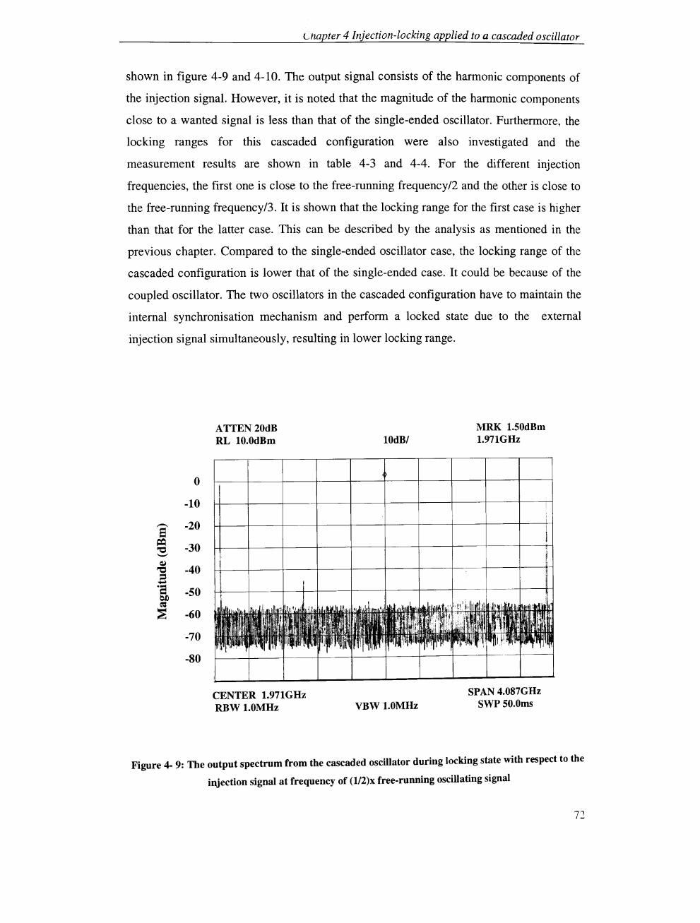
cnapter 4 Injection-locking applied to a cascaded oscillator
shown in figure 4-9 and 4-10. The output signal consists of the hannonic components of
the injection signal. However, it is noted that the magnitude of the harmonic components
close to a wanted signal is less than that of the single-ended oscillator. Furthermore, the
locking ranges for this cascaded configuration were also investigated and the
measurement results are shown in table 4-3 and 4-4. For the different injection
frequencies, the first one is close to the free-running frequency/2 and the other is close to
the free-running frequency/3. It is shown that the locking range for the first case is higher
than that for the latter case. This can be described by the analysis as mentioned in the
previous chapter. Compared to the single-ended oscillator case, the locking range of the
cascaded configuration is lower that of the single-ended case. It could be because of the
coupled oscillator. The two oscillators in the cascaded configuration have to maintain the
internal synchronisation mechanism and perform a locked state due to the external
injection signal simultaneously, resulting in lower locking range.
o -10
-20
-30
-40
-50
-60
-70
-80
ATTEN20dB RL lO.OdBm
CENTER 1.971GHz RBW 1.0MHz
lOdBI
VBW 1.0MHz
MRK 1.50dBm 1.971GHz
SPAN 4.087GHz SWP50.0ms
Figure 4- 9: The output spectrum from the cascaded oscillator during locking state with respect to the
injection signal at frequency of (1/2)x free-running oscillating signal
72

-.. e ~ "C --Q,j
"C .a 'a CJl ~
~
0
-10
-20
-30
-40
-50
-60
-70
-80
Chapter 4 Injection-locking applied to a cascaded oscillator
ATTEN20dB RL 10.0dBm
CENTER 1.971GHz RBW 1.0MHz
10dBI
VBW 1.0MHz
MRK 1.5OdBm 1.969GHz
SPAN 4. 139GHz SWP50.0ms
Figure 4- 10: The output spectrum from the cascaded oscillator during locking state with respect to
the injection signal at frequency of (1/3)x free-running oscillating signal
Input power level Locking range
(dBm) (kHz)
-4 84.12
-6 42.47
-8 36.80
-10 32.23
-12 2l.2
Table 4- 3: The locking range for the single-ended oscillator with respect to the injection power levels, where the injection frequency is close to (1I2)x free-running frequency
73

Chapter 4 Injection-locking applied to a cascaded oscillator
Input power level Locking range
(dBm) (kHz)
-8 630.8
-10 460.2
-12 251.0
-14 151.1
-16 71.3
Table 4- 4: The locking range for the cascaded oscillator with respect to the injection power levels,
where the injection frequency is close to (1/3)x of free-running frequency
4.5 Conclusion
An injection-locked cascaded oscillator is presented in this chapter. By using the power
combining approach, the directional coupler is connected between the two identical
oscillators. The advantage for this configuration is that a) it is simple in construction and
b) the coupler gives high port-to-port isolation, resulting in minimal interaction among the
devices. Furthermore, the circuit provides the phase noise improvement as shown in the
experimental results. However, instead of focusing on the optimized power combining
this work is concerned with the sideband suppression due to the subharmonically
injection-locked phenomena in the single-ended oscillator. Then, the investigation of the
injection-locked cascaded oscillator is considered, where the injection frequency is close
to (1I2)x and (l/3)x the free-running frequency. As a result, the sidebands are
significantly reduced by more than 30 dB for both cases. Moreover, the locking ranges of
both single-ended and cascaded oscillators were measured. The locking range of the
single-ended oscillator is higher than that of the cascaded oscillator. This might be due to
the limitation of the coupled configuration.
7.+

Chapter 5 Frequency Doubler Design Configurations
Chapter 5
5 Frequency Doubler Design Considerations
5.1 Introduction
Frequency doublers can be used to extend the operation range of an oscillator since there
is the limitation on the fundamental oscillators of a given technology. Also, there is a high
demand for RF sources with excellent frequency stability and low phase noise in
communication systems. Such a local oscillator might consist of a low phase-noise
fundamental source followed by a chain of frequency doublers and amplifiers. For the
multiplication process, a nonlinear transfer characteristic is required [54] which involves
the nonlinear relationship between output current and applied voltage to the device.
Suitable nonlinear devices can be diodes, bipolar transistors, MESFETs, and HEMTs.
This chapter studies the design and operation of MESFET frequency doublers. The use of
the MESFET as the frequency doubler is attractive since the MESFET frequency doublers
have the advantage of providing conversion gain and also have some isolation between
input and output ports [55]-[56]. MESFET frequency doubler design is focused on the
consideration of operating point. For optimum nonlinear operation, the device can be
biased either in the vicinity of pinch-off or in the vicinity of forward conduction where
the gate-source voltage swings between pinch-off and zero volts [54]-[60].
The other basic and important design consideration is the circuit topology. Since the
unwanted components appear at the drain, the required frequency component can be
obtained by utilising either a single-ended or balanced doubler topology. However, the
input and output matching networks are also considered. The input network should be
designed to achieve a maximum power to the device at the fundamental frequency whist
75
Chapter 5 Frequency Doubler Design Configurations
the output of the device is matched for maximum output power at the second harmonic
frequency. These design considerations are described in this chapter.
Additionally, the practical example of an injection-locked balanced oscillator and doubler
is demonstrated. An idea of this example is the integration of the balanced oscillator [61]
and balanced doubler circuits. By using the injection-locked balanced oscillator
technique, the entire circuit gives a low-phase noise signal. Also, the external balun for
the balanced configuration is eliminated, resulting in small circuit size.
5.2 General Doubler Design Considerations
In the microwave region, the Schottky barrier diode, the bipolar transistor and both
single-and dual-gate MESFETs can be used for frequency doublers due to their nonlinear
device characteristics [54]. The nonlinear transfer characteristic of the devices is the
important key mechanism for the frequency doublers. This transfer characteristic can be
described by an expansion of a Taylor series. From many applications, the MESFET is
considered because of its potential for providing gain [54].
The aim of this section is to consider the MESFET operation as a frequency doubler and
investigate the gate-source bias conditions. MESFET frequency doublers can be classified
into two bias conditions: operating at gate-source voltage in the vicinity of pinch-off and
between pinch-off and zero voltage. To achieve the frequency doubler design, the
MESFET must be kept stable. Similar to amplifier design, the stability factor K is
considered [57].
Also, various doubler design topologies are introduced. One is the single-ended frequency
doubler. From many previous studies, many techniques to obtain good performance for
the single-ended doublers are considered. The other topology is the balanced frequency
doubler. This design topology basically provides the wider bandwidth compared to the
single-ended topology.
76

Chapter 5 Frequency Doubler Design Configurations
5.2.1 Biasing considerations
As described by R.Gilmore [54], a basic concept of the multiplier process can be
introduced by considering a nonlinear device such as a diode. The transfer characteristic
of the diode can be explained by using a Taylor series as follows:
The transfer characteristic is given by
(5.1)
Where g is the nonlinear function of the device, io is the output current and Vi is the
applied input voltage.
By using a Taylor series, an expansion of g(Vi) is given by:
(5.2)
Substituting Vi = AcosUljt, then we get
(5.3)
From equation (5.3), the output current consists of dc, fundamental frequency and
harmonic frequency components. The principal objective of the frequency doubler is to
obtain only the second harmonic component and to minimize other current output
components. To achieve this objective, a bandpass filter is ideally required in order to
eliminate all unwanted current output components
From many applications [9], [54]-[68], the MESFET has been used for the nonlinear
device in a frequency doubler. The main principle of the MESFET frequency doubler is
the half-wave rectification in the gate-channel Schottky junction, with a relatively high
reverse breakdown voltage [9]. A half-wave cosine waveform is obtained at the drain
77

Chapter 5 Frequency Doubler Design Configurations
terminal. Thus, the efficiency and the output power of the frequency doubler's signal is
dependent upon the biasing point and the output resonator to eliminate all unwanted
voltage components except the second harmonic component. This can be clearly
explained by introducing the MESFET model. Figure 5-1 a) and b) show the physical
form and nonlinear model of the GaAs MESFET, respectively.
Epitaxial layer
Buffer layer
Semiinsulating substrate
s
Source Gate
a)
Cd
b)
Drain
Depletion
region
s
Figure 5- 1: a) The physical form and b) the nonlinear model of the GaAs MESFETs
78

Chapter 5 Frequency Doubler Design Configurations
By applying the gate-source voltage, V gs, and the drain-source voltage V ds, there is a
depletion region under the gate. As the drain-source voltage is increased, the voltage
across the region is greater at the drain end, resulting in the wider depletion region at the
drain end. The current channel becomes narrower due to the longitudinal electric field.
This causes the electrons to move through the channel faster, so the drain current is
increased. However, the velocity of the electron is limited, to approximately 1.3xl07 cmls
in GaAs, and the current does not increase after the drain-source voltage is increased
beyond the value that causes velocity saturation [11].
It is noted that MESFET operation is dependent on the charge mechanism due to the
MESFET's structure and the biasing voltage. This causes the Schottky-barrier formation.
In the MESFET nonlinear model, there exist two capacitances: gate-source capacitance,
Cgs, and gate-drain capacitance, Cgd, associated with the Schottky barrier. These
capacitances are generally nonlinear and are gate-source and drain-source voltage
dependent. Also, the Schottky barrier gives the two diodes [57]. One is drain-source
diode, Dgs, and the other is gate-drain diode, Dgd. Cds is the drain-source capacitance,
which is the metalization capacitance. It is treated as a constant. The other parameters in
the nonlinear model are the gate, source and drain ohmic contact resistances, which are
represented by Rg, Rs, and Rct, respectively. Ri is the resistance of the semiconductor
region under the gate. Moreover, the controlled drain current source !ct, is the important
parameter in the designed circuit and its value relies on the voltage across the gate-source
capacitance.
In the nonlinear model, the input capacitor Cgs and series resistance Ri of the gate-source
junction can be analysed as a lossy diode [59]. The value of the gate-drain capacitance
Cgd also contributes to device nonlinearity. However, this capacitor is, in general, not an
important factor in harmonic generation since the gate-drain capacitance becomes small
as the drain-source voltage increases [69]. Figure 5-2 shows the regions of operation for
frequency doubler operation [54]. In region A, where the bias is near pinch-off, the
MESFET's channel conducts only during the positive half cycle of the input sinusoidal
signal. Thus, the drain current is given as a form of a half-wave rectified signal. Also.
when the gate-source bias is near zero voltage below the forward conduction point (in
region B), the voltage waveform is clipped
79

Chapter 5 Frequency Doubler Design Configurations
<' E -
40 ,-------------------------------------....... _. __ ..... _ .... -..... ----·----1Vgs=OV --- .. -~
-------_ ... -----_._----_. __ .... -._--_._. .-.. _ ..... -_ .. Vgs=-O.222V
i / / ;' ____ .- -' - Vgs=-o.444V
,f // ___ .. ______ -.-- ._--_.--! / //-
/ /;/ _.------. _ _ .... _ .. ___ ..... _ ... _.- -- Vgs=-O.667V Iii /_._._ .. Ii / // .. ~ ... --.---.- Vgs=-1.111 V ;i /' /1 ____ .... ---.. - ••. ---... -~ _.-_ .... _ ... -/?//==-__ . __ .......... _ ......... _- .... _ .. _ .. -._ .. _ ... _. __ -- ~9S=-~ .:::~
f:~::.~:-' - ..... --.-~::::.: ..... -- ...................... --- '. ~ ••........ -- -. V~:::2:000V -2
o 5 Vds(V)
Figure 5- 2: FET output characteristics showing the region of operation for frequency doubler
operation
5.2.1.1 V gs near pinch-off (Class B)
The active device in a class B multiplier is biased in the vicinity of pinch-off. Figure 5-3
shows waveforms and signal trajectory for a class B multiplier [57]. Ideally, the active
device conducts when the input voltage is more than pinch-off. With proper output
matching at the second harmonic frequency, the class B doubler provides the second
harmonic output power given by the product of the second harmonic current component
and the voltage component. The rms average power is obtained [57] as:
(5.4)
80

Chapter 5 Frequency Doubler Design Configurations
IDS IDS IDS(t) .,. . '
IF +~" ,"\
\
1\ I,'
\ I~, " I!
\
I ' Ii ! " "
I'
l :i
'~ i "~
I I
VGS ~) VDS I I ~ I ..
==--::> .. _.---
t t
Figure 5- 3: Waveforms and signal trajectory for class B multiplier
5.2.1.2 V gs in the vicinity of forward conduction and between 0 volt and
pinch-off
In this mode, the device is biased between 0 volt and pinch-off and if the input swing is
large enough, the output at the drain is clipped at both ends. If the output wavefonn is
symmetrical, the even harmonic components will be smaller than the odd hannonic
components [65]. When the PET is biased close to 0 V, the voltage wavefonn across the
gate-source capacitance is clipped due to the junction conduction [59] and will be half
wave rectified due to the conduction cycles operated by the gate-source diode [65]. This
rectified waveform is transferred to Ids through the device transfer characteristic. By
Fourier analysis, the half-wave rectified waveform consists of a fundamental and a second
harmonic voltage of V /2 and 2V / 31l [59], respectively. Where V represents the drain
source voltage.
81
t

Chapter 5 Frequency Doubler Design Configurations
5.2.2 Frequency doubler design topologies
5.2.2.1 Single-ended frequency doubler
Figure 5-4 shows a basic single-ended frequency doubler configuration. A quarter
wavelength open-circuited stub is often used in the single-ended frequency doublers [11],
[57] to supress the fundamental frequency component at the output. The rest of the design
is to consider the input and output matching networks corresponding to fundamental and
second harmonic frequencies, respectively.
Input at fo
r·································~
: i I JJ4 :
~------~ i ! i at fo i Input
Matching atfo
! ! i i : i i ! :
I , i :
:. ................................ J
f····························j i ! i ! ! i j ! ! ir-------~
: : Output i ~
: ! 1J4 i at fo i L ............................ ~
Matching at 2fo
Output at 2fo
Figure 5- 4: The frequency doubler employing A / 4 transmission lines
For high performance single-ended PET frequency doublers, there are many previous
studies examining the input and output networks. Gilmore [54] stated that the optimum
output load at fo is an open circuit shifted by the conjugate of the output capacitance of
the PET. Furthermore, the reflection network has been used in the frequency doubler.
Rauscher [55]-[56] and Borge [60] presented a design method of the second harmonic
reflector type at the output PET frequency doubler. Rauscher's study [55]-[56] explained
that the optimum output load at the fundamental frequency was a short-circuited stub at
an optimal distance from the PET drain. Borge used the same technique in the Darlington
doubler employing bipolar transistors. In addition, other studies are based on the use of
reflector networks. There appear that the input and output reflector networks used in the
PET and HEMT frequency doublers by Iyama [67] and Thomas [68], respectively. For
the latter work, Thomas stated that these reflection networks function as both filtering and
82

Chapter 5 Frequency Doubler Design Configurations
matching for the input and output of the doubler. The second harmonic component is
reflected back into the gate at the proper phase angle as well as the fundamental signal
being properly phased into the drain. As a result of the effect of proper reflection phase
angle, the optimum conversion gain can be obtained.
5.2.2.2 Balanced frequency doublers
The other popular doubler design is a balanced (push-push) doubler [57] which is shown
in figure 5-5. In a balanced frequency doubler, the quarter-wavelength open-circuited stub
is not required. The balanced circuit consists of a pair of nonlinear elements and a 180-
degree input balun [11], [57]. The applied input power is divied by the balun. These anti
phase inputs are then applied to the two FETs. As a result, the two FETs conduct on
alternating half-wave cycles. Due to the balanced configuration, the second harmonic
components from each drain device are combined in phase whilst the fudamental and
other odd harmonic frequency components are subtracted, combining out of phase.
Therefore, the second harmonic components are summed in power.
Input Matching
/). Output
Input Matching Output
at fo L at 2fo
Input Matching
Figure 5- 5: A balanced (push-push) doubler
The advantage of the balanced frequency doubler is that it gives the elimination of the
fundamental and odd-harmonic frequency components. Also, the wide bandwidth is
obtained [11], [57], althougth the bandwidth of the balanced frequency doubler is limited
by the balun and the imbalance of devices which are ideally identical. Another important
83

Chapter 5 Frequency Doubler Design Configurations
point is that the input and output power can be attenuated due to the insertion loss in the
balun and the power combiner, respectively. This can degrade the conversion gain of the
balanced frequency doubler.
5.3 Practical example of an injection-locked balanced oscillator and
doubler
The demand for high performance oscillators is rapidly increasing in microwave and
millimetre-wave applications. In an advanced millimetre-wave communication system,
such as LMDS (Local Multipoint Distribution System), it has been reported [62] that the
phase-noise of local oscillators in the upconversion and downconversion chain is the main
noise contribution, degrading the bit-error-rate of the communication system. For
collision avoidance radar systems, signals with low phase-noise are also required [63]. To
achieve a highly stabilised signal in the millimetre-wave and microwave bands, several
techniques have been proposed, including the phase-locked loop, injection-locked
oscillators with frequency multipliers, dielectric resonator oscillators, and a number of
other techniques [4]-[5].
The injection-locking technique with frequency multiplication is attractive for generating
a stabilised source in many applications due to its simplicity and low component count. In
Chapter 3, the injection-locked balanced oscillator was described [61]. The technique is
simple and consumes low DC power. Also, it provides balanced stabilised signals with no
external balun, resulting in a small circuit area. In this section, the sub-harmonic
injection-locked balanced oscillator signals directly apply to a balanced frequency
doubler as input. This eliminates the high performance balun, which is required in a
conventional circuit. The technique is demonstrated experimentally in the S-band.
5.3.1 Circuit realisation
The circuit diagram of the proposed balanced oscillator-doubler is shown in figure 5-6.
The sub-harmonic injection-locked balanced oscillator provides a pair of balanced
outputs, at half the final output frequency. These outputs have previously been shown to
have a precise 180-degree phase difference and amplitude balance; more precisely

Chapter 5 Frequency Doubler Design Configurations
balanced, in fact, than is normally obtained with a balun. As mentioned in previous
chapters, the balanced oscillator is based on the extended resonance technique, with a
transmission line connected between the gates of the two active devices, so that the two
active devices resonate with each other [7], [61]. Series feedback, using a short-circuited
stub, is applied at the source of each active device to produce negative resistance. A sub
harmonic injection-locking signal is applied to the balanced oscillator through the
matching network (M}) at half the free-running frequency. This matching network is
connected at the mid-point of the transmission line between the gates of the active devices
in order to maintain the balanced configuration. The outputs of the balanced oscillator are
immediately fed into a balanced doubler.
I···························································· .. ···r······························································T····················· ············1
i I I I : ~
:
Subharmonic Ml
Injection
Signal, fol2
Wilkinson
Balanced oscillator ! i Doubler combiner !
i !
Balanced
! 1 ! ! : ~ .......................................................................................... .J ..•..••.•.•.•.....•.•••.....•.•..•..•...••.•••..•....•..•..•••..•.. _ ...................... .-..-.. _ .. _ ................. _._ •.•••. _.
Output at2fo
Figure 5- 6: The circuit diagram of the novel sub-harmonic injection-locked balanced oscillator
doubler configuration
85

Chapter 5 Frequency Doubler Design Configurations
A balanced doubler consists of two identical doublers and a Wilkinson divider. These two
frequency doublers operate at 2-to-4 GHz. The doubler configuration is illustrated in
figure 5-7. The doubler design concept is based on GaAs PETs biased near zero gate
source voltage [64]-[65]. The optimal matching networks at the fundamental frequency
and second harmonic frequency are used to terminate the input and output of the active
device, respectively. The input and output ports of the doubler are conjugately matched in
order to achieve the maximum power into the input port and to obtain the maximum
power at the output port. In this case, external feedback is used in this doubler design to
compensate for the transistor internal feedback. The external feedback is for
counteracting or complementing the parasitic feedback effects [55], resulting in the
elimination of the parasitic feedback at the frequency of the second harmonic [56]. The
external feedback in the doubler is found to increase the conversion gain, but also
degrades the bandwidth.
r--------------------------------------------------------------------------------------, , ' , '
! (Optimal fo and 2fo external feedback) ! ! ! b <5-------------------------------------------------------~ ~
: : ' I
Input Matching Network
Output Matching Network
Figure 5- 7: Single-ended doubler circuit configuration
The outputs of the two devices in the balanced doubler are combined in a Wilkinson
divider, designed at twice the frequency of the oscillator. At the output of the balanced
doubler the even frequency components are summed, whereas the odd frequency
components - including the fundamental frequency from the oscillator - are cancelled out.
86

Chapter 5 Frequency Doubler Design Configurations
Basically, the Wilkinson power divider functioning as a power combiner consists of t 0
wave sections [8] as shown in figure 5-8. The characteristic impedances of these two
sections - connecting in parallel wi th the input line - are Z2 and Z3, respectively. Since the
Wilkinson power divider operates as a 3-dB power divider. The characteristic impedance
of Z2 and Z3 is equal to .fi Zo, where Zo is the input impedance.
Figure 5- 8: The Wilkinson power divider
5.3.2 Results and Discussion
The sub-hannonic balanced oscillator was designed and fabricated using FR4 board and
Infineon CFY30 OaAs PETs as active devices. The oscillator was designed to operate at
about 20Hz, so that the output of the complete circuit was at almost 40Hz. The balanced
oscillator and the doubler circuits were biased at V ds = 2.2 V, V gs = -0.97 V and V ds = 3.0
V, Vgs = -0.3 V, respectively. From this, the balanced oscillator gives a free-running
frequency of 1.9460Hz. Also at the output of a power combiner the second harmonic
frequency component is -0.67dBm, whereas the fundamental and the third harmonic
components are -18.67dBm and -23 .67dBm, respectively. Figure. 5-9 shows the output
spectrum of the balanced oscillator-doubler. These measured results include a 3-dB
attenuator and 0.5-dB cable loss at the output port.
7

-..
= = "'0 --Qi "'0 ::s ...... 'a OJ) ec ~
0
-10
-20
-30
-40
-50
-60
-70
-80
ATTEN20dB RL lO.OdBm
CENTER 3.893GHz RBW 1.0MHz
Chapter 5 Frequency Doubler Design Configurations
lOdBI
VBW 1.0MHz
MRK -O.67dBm 3.901GHz
SPAN 5.000GHz SWP IOO.Oms
Figure 5- 9: The output spectrum of the balanced oscillator-doubler circuit (with 3-dB attenuator and
without sub-harmonic injection-locking signal O.5-dB cable loss at the output)
To investigate the use of the injection-locked oscillator with the balanced doubler, a
subharmonic locking signal of 974.8 MHz with a power level of -2.0dBm was injected
into the balanced oscillator. It was noticed that with the integrated balanced oscillator and
balanced doubler the oscillator still maintained balanced characteristics. In the locking
state, the magnitude and phase of the balanced oscillator are equal with 180-degree phase
difference. The power output of the balanced oscillator-doubler is slightly degraded, but
the phase noise of the output signal is improved. Figure 5-10 illustrates the measured
output in the locking state compared to that output without injection signal. The phase
noise is reduced more than 15 dB at the offset frequency of 50 kHz. Moreover, the
locking range as a function of the injection power level was investigated. Figure 5-11
shows the measured locking range of the sub-harmonic injection-locked oscillator-
doubler for injection power levels from -4 dBm to 4 dBm.
88

Chapter 5 Frequency Doubler Design Conjigul"uJ,v)d
o -10
-20
-30
~ -40 .a 'c -50 ?I ~ -60
-70
-80
ATTEN20dB RL 10.0dBm
Output with injection-locking
10dBI
CENTER 3.8936640G Hz RBW3.0kHz VBW3.0kHz
MRK -1.67dBm 3.8936640GHz
Output without injection signal
SPAN 500.0kHz SWP 140ms
Figure 5- 10: The comparison between the output of the balanced oscillator-doubler, with and
without subharmonic injection-locking signal (0.5dB cable loss at the output and 3dB attentuator)
"........, 1600
~ 1400 '-'
~ 1200 "'0 1000 '~ "'0 800 = ~ .0. 600 ell = 400
:£2 ~ 200 0 ~
0
-4 -2 0 2 4
injection power (dBm)
Figure 5- 11: The measured locking range of the subharmonic injection-locked oscillator-doubler as a
function of injection power level
89

Chapter 5 Frequency Doubler Design Configurations
5.4 Conclusion
In design of frequency doublers , the input signal is fed into nonlinear devices, such as
diodes and PETs. The input and output matching circuits are used to short circuit at all
unwanted harmonics of the excitation frequency at the input and output, respectively.
Practically, the input impedance is conjugately matched to the active device so that the
maximum energy can transfer from the source to the device. In addition, the resonant
circuit is employed to provide the output matching at the desired harmonic.
Since the frequency doublers exploit the MESFET's nonlinearity [11], [57], the
performance of the doubler is dependent on bias point and the design topology. To
achieve a good doubler design, the nonlinear device is used in the stable condition, like
the design procedure for amplifiers. For the biasing consideration, the PET biased in the
vicinity of pinch-off generates a half-wave sinusoidal current being rich III even
harmonics [57]. The device functions as a half-wave rectifier, resulting III good
efficiency. Another biasing case is near zero voltage producing the waveform close to the
half-wave rectified waveform. In this region, the device can give a high output voltage.
However, there can be an unacceptable conversion loss and high dc power dissipation in
the active device. The other important design consideration is the choice of topology: a
single-ended or a balanced frequency doubler. The basic design principles for these
doublers have been explained. Also, the design techniques to improve the single-ended
doubler have been summarised.
As the applicable example, an injection-locked balanced oscillator and doubler has been
introduced. By using the reflector network type [55]-[56], the balanced frequency doubler
gave good conversion gain. The injection-locked oscillator is also used in order to
stabilise the oscillating signal. This example shows the feasibility of the integrated
balanced oscillator and balanced doubler. The advantage of this work illustrates the low
phase noise output signal and small circuit size because the external balun is not required.
90

Chapter 6 Frequency Doubler using Feedforward Technique
Chapter 6
6 Frequency Doubler • uSing Feedforward
Technique
6.1 Introduction
There is a great demand for high spectral purity signals in microwave and millimetre
wave communication and radar systems. Frequency multipliers are widely used in a
variety of applications, especially in frequency translation circuits, in order to extend the
frequency limit of fixed or variable frequency low phase-noise oscillators. Several
doubler techniques have been studied in the literature [55]-[56], [70]-[72]. Active
multipliers, in general, provide conversion gain and wider bandwidth compared to the
varactor diode type. The nonlinear transconductance is the most important mechanism for
a harmonic generator. Active doublers, such as FET doublers, are normally used at a bias
point in the vicinity of pinch-off, allowing the active devices to generate a high level of
even harmonics. There are two main doubler circuit design techniques as described in the
previous chapter. One is the use of quarter-wavelength open-circuit stub. This technique
is often used in a single-ended doubler to suppress the fundamental frequency at the
output [67]. Another popular doubler design is a balanced doubler technique. In this
topology the fundamental frequency is cancelled out due to the summation of odd
harmonics which are out-of-phase at the output of the circuit, whist the second harmonic
is added [63], [66], [70]. However, these doubler design techniques generally provide
only 25dB of fundamental signal suppression due to the practical limitations of open-stub
and balun circuits in the single-ended and balanced doublers, respectively. For fully
monolithic transceivers it is highly desirable to increase the fundamental suppression.
91

Chapter 6 Frequency Doubler using Feedforward Technique
In this chapter, a new method of fundamental frequency suppression in a frequency
doubler is proposed. The feedforward technique has been widely applied for distortion
cancellation in amplifiers [40], [73]-[78]. The principle of the feedforward technique in a
power amplifier is viewed as the sum of a replica of the input and error signals as shown
in figure 6-1. The degree of distortion cancellation in the power amplifier is dependent on
the carrier suppression in the signal cancellation loop, and having good phase and
magnitude balance in the error cancellation loop [40].
Main power amplifier
Vin delay 2 + Vout
(jerror c::Oc;'/atJon _
attenuator
signal cancel/atlo
(j de/ay1
Error amplifier
Figure 6- 1: Feedforward technique for a linearised power amplifier
The use of the feedforward technique for substantially eliminating the fundamental
frequency component of the frequency doubler is described. To do this, a simplified
representation of using the feedforward technique for fundamental component
suppression in a I-to-2GHz frequency doubler is demonstrated. Unlike the use of the
feedforward technique in power amplifiers, the output of the frequency doubler itself has
to be well estimated in order to ensure the magnitude balance between the fundamental
components of the doubler output path and the reference path. Also, the phase balance
between these two paths is determined in advance.
92

Chapter 6 Frequency Doubler using Feedforward Technique
To demonstrate the fundamental suppression by using the feedforward technique, the
design of the 1-to-2GHz doubler and the 1GHz directional couplers functioning as a
splitter and subtractor are presented. In the doubler design, a filter is required to first
suppress the fundamental component at the doubler output; otherwise, the fundamental
power level of this path will be larger than that in the reference path. The fundamental
component cancellation may not occur at the output of the second coupler. Additionally, a
reflection-type analogue phase shifter is also designed at 1 GHz. This phase shifter is used
to adjust phase balance of the fundamental frequency components between the reference
and the doubler paths.
Due to the amplitude and phase imbalance between the doubler and the reference paths,
the measurement results show the degree of fundamental suppression at the output of the
second directional coupler: More than 50dBc fundamental frequency suppression can be
achieved. The measured second harmonic output and the fundamental frequency power
levels as a function of the input power levels are also demonstrated.
6.2 Design
Figure 6-2 illustrates the feedforward technique for fundamental signal suppression in the
frequency doubler. The circuit consists of a 1-to-2 GHz frequency doubler, phase shifter,
and input and output couplers. The input power is split into two paths by using coupler 1.
One goes to the reference path, consisting of a phase shifter, and the other goes to the
main path, consisting of the frequency doubler. The reference path is generally chosen to
have low loss and is also used to adjust the phase balance. Substantial fundamental
component cancellation occurs when the fundamental frequency power of the two paths is
added in anti-phase by employing coupler 2. Therefore, the coupler 2 functions as a
subtractor for the fundamental component.
93

Chapter 6 Frequency Doubler using Feedforward Technique
IGHz Input
Coupler 1 Coupler 2 I-to-2GHz
Multiplier
<I>
Variable phase Variable gain/attenuator
(may be needed)
2GHz Output
Figure 6- 2: Feedforward technique for fundamental signal suppression in a frequency doubler
In order to achieve the maximum fundamental frequency cancellation, the magnitude and
phase of the outputs of frequency doubler and phase shifter are determined. Ideally, the
magnitude and phase of the fundamental components between these two outputs must be
equal and I80-degree out-of-phase. Therefore, the degree of cancellation relies on the
fundamental power level of the doubler output and the two couplers. Also, it is dependent
on the phase adjustment of the phase shifter.
Frequency doubler path consists of frequency doubler and filter. With the filter connected
at the output of the frequency doubler, the power level of the fundamental component is
less than the power level of the second harmonic component at the output of the
frequency doubler path. Compared to the reference path, the fundamental power level at
the output of the filter in the doubler path should be the same as the power level in the
reference path, so that the fundamental component can be cancelled out by using coupler
2, which functions as the subtractor.
In the feedforward system, the higher input power generally occurs at the doubler to
produce the high power level of the second harmonic output. The small coupling factor is
94

Chapter 6 Frequency Doubler using Feedfonvard Technique
considered. Like the coupler!, the coupler 2 should also have small value of the coupling
factor. If the coupling factor of coupler 2 is high, the second harmonic component will be
degraded at the output of the coupler 2. The other reason for small coupling factor is that
the insertion loss is smaller.
A reflection-type analogue phase shifter is used for phase adjustment in the reference
path. The designed circuit is fabricated on FR4 board and the BB833 diodes are used as
the varactor diodes in order to control the tuning phase. Also, both the measured phase
and insertion loss are tested.
6.3 Circuit Realisations
6.3.1 Single-ended Doubler Design
The doubler design is based on the PET active device biased in the vicinity of pinch-off.
This leads to an output signal rich in even harmonics. Figure 6-3 shows the doubler
circuit configuration [55]-[56]. The output of the active device is optimally matched so
that maximum output power can be obtained at the designed harmonic, 2fo. This output
matching network also functions as a bandpass filter, providing some suppression of the
fundamental and other harmonic frequencies.
,.----_.-----------_ ... -------------------------------------------------------------------, , , , , i (Optimal fo and 2fo external feedback) i : I , , , , , , I I : .--------------------------------------------------------¢ ¢
<> ¢ , , : : I I
Input Matching Network
ZIN
Output Matching Network
Figure 6- 3: Single-ended doubler circuit configuration
95

Chapter 6 Frequency Doubler using Feedforward Technique
The input matching network is used to achieve matching into the gate of the device at the
fundamental frequency. Practically, the input port and output port of the doubler are
conjugately matched at the fundamental frequency and second harmonic frequenc .
respectively. An important aspect of this circuit is that this doubler configuration utilises
external feedback. Due to the transistor internal feedback, the incorporated external
feedback is for counteracting the parasitic feedback effects [55]. This eliminates the
second harmonic parasitic feedback loss [56] . However, the use of the second harmonic
feedback involves a direct trade-off between the conversion gain and bandwidth. In this
case the external feedback is employed in order to increase the conversion gain for the 1-
to-2GHz doubler. The doubler design in this work focuses on using the feedforward
technique to dramatically reduce the fundamental signal at the output.
The I-to-2GHz frequency doubler was designed and constructed on FR4 using Infineon
CFY30 GaAs FETs as active devices. A transmission line with coupling capacitors is
used to implement the external feedback. To investigate the effect of the external
feedback, the input and output matching networks are designed to match 50-ohm for the
fundamental and second harmonic frequency, respectively. This was achieved by using
harmonic-balance analysis in the Libra program. Figure 6-4 shows the doubler circuit
board using the external feedback, based on FR4.
~VDS
Input,
Figure 6- 4: Single-ended doubler circuit
Output. f· ut= ~fin
,/

Chapter 6 Frequency Doubler using F eedforward Technique
In order to achieve the fundamental frequency cancellation the magnitude of the
fundamental frequency between the doubler and the reference paths are carefullv
examined. The magnitude of the two paths should be accurately estimated. A filter is
introduced in the doubler path. In this case, the coupled line is used to function as the
lumped elements [78]. A coupled line can be modelled as an equivalent lumped element
circuit. The filter configuration is shown in figure 6-5. Also, figure 6-6 illustrates the
simulation result. From this, the signal can be suppressed at the frequency of 1 GHz whist
the second harmonic is passed at the frequency of 2GHz.
Port 1
Port 2
Figure 6- 5: Filter configuration
+ 511 )( 512 .522
0.0 '--'---Ci;::::=:p~,----r::l
iii' -10.0 "C -Q)
-g -20.0 I--+l+--H+---ti--r--t--t--i ~ r::: C) CIS :E -30.0 1---lI---J---+-\t----t--t----"1
-40.0 0.0
Frequency 1.0 GHzlDIV
Figure 6- 6: Simulation result of the filter
6.0
97

Chapter 6 Frequency Doubler using Feedfonvard Technique
6.3.2 Reflection-type analogue phase shifter and directional coupler
A phase shifter is represented as the variable phase block shown in figure 6-2. The
function of the phase shifter is steady control of the relative phase between the input and
output with a flat group delay frequency response [5]. A reflection-type analogue phase
shifter consists of a 3-dB Lange coupler and terminating impedances, ZT, reali sed with
varactor diodes. Figure 6-7 and figure 6-8 show the reflection-type phase shifter
configuration and its layout. The desired phase shift can be obtained by changing the bias
of the varactor diodes. This phase shifter was designed for 1 GHz based on FR4. The
BB833s are used as the varactor diodes. Also, a pair of lOdB directional couplers was
constructed on FR4.
3dB quadrature directional coupler
~ / identical reflection terminations
Figure 6- 7: The reflection-type phase shifter configuration
..- Tuning voltage
Figure 6- 8: The layout of reflection-type phase shifter at IGHz
9

Chapter 6 Frequency Doubler using Feedfonvard Technique
6.4 Results and discussion
The filter performance was first investigated. Figure 6-9 shows the measurement result
from the network analyser. This result offers a good agreement with the simulation result
as shown in figure 6-9. With the filter connected to the doubler, the complete doubler
circuit was biased at VDS = 3.0 V and VGS = -2.2 V, relative to a pinch-off voltage of -2.0
V. An input power level of -ldBm was applied to the doubler. Figure 6-10 shows the
output spectrum of the frequency doubler without applying the feedforward. It shows that
the power level of the fundamental component is -26.17 dBm. This measured result is
taken from an HP8563E spectrum analyzer, which is connected via a 3-dB attenuator and
a cable with 0.5-dB loss. Therefore, this doubler provides 0.5 dB gain. Compared to the
doubler output without connecting the filter, the power level of the fundamental
component is reduced by approximately 23 dB. However, the second harmonic
component is slightly degraded due to the insertion loss in the filter.
+ 511 0521 .522
m -1 O.O---ir---~f----f----\+---+-------j
" -Q)
" :l ~ C 0) n:s :E ·30. Of--------fJf--t-------tt---Jf------i----tH
-40. 0 L.-__ J.. __ ---L ___ --L-__ --'
0.0 4.0 Frequency 1.0 GHzlDIV
Figure 6. 9: The measurement result of the filter from the network analyzer
99

-10
-20
-30
-40
~ -50 .a -a -60 Oil ~ ~ -70
-80
-90
Chapter 6 Frequency Doubler using Feedforward Technique
ATTEN 10dB RL OdBm 10dBI
MRK -4.00dBm 2.000GHz
r-~---+---+--~--4---~-----, -
CENTER 2.000GHz RL 1.0MHz VBW 1.0MHz
SPAN 2.2S0GHz SPW SO. Oms
Figure 6- 10: Output spectrum of the 1-to-2GHz doubler without the feedforward technique (with a
3-dB attenuator and O.S-dB cable loss at the ouput)
To investigate the fundamental frequency suppression technique, the two couplers and
reflection-type phase shifter were connected as shown in Figure 6-2. The phase of the
phase shifter was tuned by varying the voltage applied to the varactor diodes. The phase
is variable between _35 0 and 1400 while the insertion loss varies between -1.9 and 0 dB
as shown in figure 6-11.
100

Chapter 6 Frequency Doubler using Feedforward Technique
140
120
100
- 80 ~ ;..
60 OJ) Q,I
"'0 -Q,I 40 rIl ~ .c 20 ~
0
-20
,,--r---r- - i"",
~J--J- __ ~ _____ ~J_~~_~~ , • , I I ,', . I • I ,
+----------~---- ------~-------~~----~~-~--i , I ,i I I ii, ' ,
+------------ ----------~--------------~-~ I' ,. " I I I I 'I + ~ -.. _1- •• _'_ _ _ _ _ __ ' ___ ' _ ~ __ ~. _' ___ ' ______ ~ __ .• _: _ ~ __
. I , I •
t I • •• I I h (d '\ __ .. __ .. __ .. _________ .. __ .. __ -+-p ase eg ree J
.... ' I Ii, 'I .• - -
•• , I • , 'I ----s (dB) I I _~_ ___ _ ~~~2~1~~~~~
..., ", - - - - -. - - -. - i - - i - ,--= -,- - - - - - i - - - - - i -I-
I ~'illlllll'IIII",
I I I I I I I I I I I I I .~ I ' I I I I I I I , I I I' I
: - - - ,- : - ,- ~ - - ~ ..... j -if • -.- .. ----.. ----- ~ --
0
-0.2
-0.4
-0.6
-0.8 -~ -1.0
"'0 --N
-1.2 rF1
-1.4
-1.6
-1.8 -40 , I I I I I I I I -2.0
Tuning voltage (Volts)
Figure 6- 11: Phase and insertion loss of phase shifter
After adjusting the phase of the fundamental frequency component from the feedforward
path and the doubler path, the signals from the two paths are combined using the second
coupler. Consequently, the output of the second coupler is observed. Figure 6-12 shows
the output spectrum of the doubler using the feedforward technique. It is clearly shown
that the power level of the second harmonic component is -5.17 dBm whereas that of the
fundamental frequency component is -65.17 dBm, where the phase of the feedforward
path is set to about 85°. A conversion loss ofO.67dB was obtained from this experiment.
Comparing the fundamental frequency power level of the doubler with and without the
feedforward branch, the fundamental frequency component is substantially improved,
with more than 50 dBc achieved at an input power level of -0.82 dBm. The second
harmonic power level is attenuated by 1.17 dB due to the loss in the additional
components. Finally, the proposed frequency doubler with the feedforward technique is
also measured as a function of input power. Figure 6-13 shows the graph of the output
power at the fundamental and second harmonic frequencies vs. the input power.
101

-10
-20
-30
-40
~ -50
2 '8 -60 ~ = ~ -70
-80
-90
ATTEN 10dB RL OdBm
CENTER 2.000GHz RL 1.0MHz
Chapter 6 Frequency Doubler using Feedfonvard Technique
10dBI
VBW 1.0MHz
~IRK -5.17dBm 2.000GHz
SPAN 2.250GHz SPW 50.0ms
Figure 6- 12: Output of the 1-2 GHz doubler with feedforward (with a 3-dB attenuator and 0.5-dB
cable loss at the ouput)
0
-1
IS -2 G -3 f"l
~ -4 .... = -5 .e-= 0 -6 ... ~
~ -7 0 ~ -8
-9
-10
I~ I I :
'J:_-::-~ .. :~:..=.-=-~....-...::...:.i:....:..:::~-~~~-~-:...:....:..:.i.:....::...:-"i~~--~--~--
N QC)
N I
, I I I j I I I I I I
__ - .., - - - - r ... - - i - ...... -1- - - - ,. - - - -,- - - - T - - - ., - - - - .... - - - , - - - ... r - - -I I I I I I I I
I I I I I I I I I I t ___ ~ ____ ~ ___ J ____ I ____ l ____ I ____ l ___ ~ ____ L ___ J- ___ L __ -
I , I I I I I I I , I , , ,. : I t I I I I I ___ .., ____ r ___ i ____ I ____ ~----,----r---.,----r---~----r---
I I I I I'
I I I I I I ____ , ____ L ___ J ____ 1 ____ .J. ____ , ____ 1 ___ J - - -
I I I I I I I I
, , ---~----~---~ ___ I_---~-- .
I I I I , , I I I I
---~----r---'-- -,--- ,----, , , ,
___ J ____ ~ ___ ~ ________ ~ ___ .
I I I I I
~ N ~ ~ N QC)
rt'l QC) ~ QC) ~ ~
N ~ ~ Q Q Q I I I I I
-J:-
QC) \C Q
at_2_GHz
at_l_GHz
Q() QC) Q() ~ '>C ~
~ ~ N
Input power (dBm)
Q() '>C N
0
-10 IS
== -20 ~ ...-4 .... eo:
-30 .... = ~ ....
-40 = 0 ... ~
-50 ~ 0 ~
-60
,.,1\ QC) ~
~
Figure 6- 13: Measured output of the frequency doubler as a function of the input power le\'el
102

Chapter 6 Frequency Doubler using Feedforward Technique
As it is seen in the experimental results, the fun dam an tal component can be suppressed to
better than 50 dBc. Using the feedforward technique in the doubler gi yes an excellent
fundamental component cancellation. However, using this technique suffers from several
shortcomings [40], similarly to the power amplifier case. First, the phase shifter in the
implementation requires passive components, such as microstrip, giving power loss. This
could affect the unequal magnitude cancellation at the second combiner which is the
second coupler. In addition, these components can possibly degrade the second harmonic
component performance. Secondly, the amount of fundamental cancellation is dependent
on the magnitude and phase matching of signals sensed by the combiner and the phase
shifter.
In order to obtain improved purity of the doubler output signal, the feedforward technique
can be applied as depicted in figure 6-14 [40]. The error amplifier is rich in odd harmonic
frequency components whereas the output of the doubler is rich in even hamonics,
especially the second harmonic component. Then, with appropriate phase and magnitude
match between the two paths, the odd harmonics can be removed by the second combiner.
Compared to the previous topology shown in figure 6.2, the the purity of the doubler
output might be improved by eliminating all odd hamonic components.
t r i r I r i 1 f f 2f 3f f 2f 3f + 2f o 0 0
0 000 0
x2 + Input
Error Output cancellation
Single loop cancellation loop
I i f 3f
Av1 0 0
Av
Amplifier Attenuator Error amplifier
Figure 6- 14: Feedforward technique for odd harmonic component suppression in frequency doubler
103

Chapter 6 Frequency Doubler using Feedforward Technique
6.5 Conclusion
The broad conclusion of this chapter is that there is more to be learnt about the subject of
fundamental frequency component elimination in the doubler by using the feedforward
technique. This chapter presents a technique to eliminate the fundamental frequency
component in a frequency doubler. The use of the feedforward technique is proposed to
be a convenient way to solve the problem associated with the purity of the output signal
in the frequency doubler. The concept of this technique is dependent upon the amplitude
and phase balance of the fundamental frequency components between the doubler and
reference paths.
The measured results demonstrate the effectiveness of this proposed technique. It is
shown that the fundamental frequency component at the output of the second coupler is
tremendously improved to better than 50dBc. In addition, this design technique is simple
and can be wide-band, depending on the doubler design topology. However, the drawback
in the use of the feedforward technique in doubler is the sensitivity and the additional loss
in the passive components, which can degrade the conversion gain of the doubler.
For the improved purity of the doubler output, the feedforward technique is also
introduced to eliminate the odd harmonics. The topology needs the error amplifier to
generate the odd harmonic components in the error cancellation loop. The purity of the
output signal is dependent on the phase and magnitude imbalance between the output of
the signal cancellation loop and the output of the error amplifier. However, this topology
can degrade the conversion gain of the doubler due to the passive elements such as
couplers.
10.+

Chapter 7 Conclusions and Suggestions for Future work
Chapter 7
7 Conclusions and Suggestions for Future
Work
The aim of this research is to improve the spectral purity performance of microwave
balanced oscillators. This is to achieve the purity improvement in the balanced oscillator
where the stabilisation and phase noise are considered. The injection-locking technique is
focused on getting a better-stabilised oscillating signal and obtaining low phase noise.
The oscillator frequency is also restricted to the limitations of the active devices. But the
restriction can be solved by using frequency doublers. A new technique to suppress the
unwanted output signals is proposed in this thesis. All the circuit designs are based on a
frequency of 20Hz for ease of fabrication.
The main achievement of this research can be summarised as follows:
• Analysis of the electrical length of the transmission line used in the balanced
oscillator, where the extended resonance technique is used to determine the
oscillator conditions for the balanced oscillator. A self-oscillating mIXer IS
illustrated as an example application of the balanced oscillator.
• Using the injection-locking technique in a balanced oscillator. This is achieved by
using the matching network connecting at the centre of the transmission line.
where it is connected between the two active devices.
• By extending Kurokawa's work, the equivalent circuit of the oscillator has been
characterised as both negative-resistance and feedback models. For a harmonic and
subharmonic injection signal, both models are used to analyse the locking range.
The harmonic signals are generated due to the nonlinearity of the active device and
these signals are fed back into the feedback network, where the negative-resistance
model is characterised. At this point the locking range is considered by using
Kurokawa's theory [21]-[22].
lOS

•
Chapter 7 Conclusions and Suggestions/or Future H'ork
The agreement between experiment results and the analysis shows that the locking
range of the injection-locked balanced oscillator for a harmonic frequency is higher
than that for the fundamental, and also higher than that for the subharmonic
frequency, when the injection power level is the same.
• The power combining technique is used for the cascaded oscillator. Rather than
focusing on the optimised combined power, the additional sidebands, which are the
effect of the subharmonic injection-locking phenomenon, are investigated. The
experiment shows that the effective sidebands are further reduced in the cascaded
oscillator compared to the single-ended oscillator. The degree of the sideband
suppression is about 30 dB.
• The PET frequency doubler design considerations are considered. To achieve gain,
the biasing and the PET frequency doubler configurations are taken into account.
An integrated subharmonic injection-locked balanced oscillator-balanced doubler
is introduced to demonstrate an example application of the frequency doubler.
• A novel technique for the fundamental frequency component supression In a
frequency doubler is introduced. The principle of feedforward, as applied to
distortion cancellation in amplifiers, is used in the frequency doubler. The
experimental result shows that the fundamental component is significantly
suppressed to better than 50 dBc.
Papers published on this research include 2 papers in the European Microwave
conference [79]-[80], one at the the IEEE Microwave MTI-S Int. Symp. Dig.[81], two at
the European Frequency and Time Forum [82]-[83] and two publications in lEE
Electronics Letters [61], [84].
There are two interesting areas as which can be pursued further. The first is to further
improve the phase noise in the oscillator: The injection-locked balanced oscillator can be
viewed as a distributed oscillator. By using the concept of the power dissipation and phase
noise [40], figure 7-1 illustrates the addition of the output voltages of N identical
oscillators. It is assumed that the noise sources of different oscillators are uncorrelated
whist the relationship between the carriers is correlated [85]. For simplicity, the addition
of two output voltages from the two identical oscillators is given as an example. Let us
106

Chapter 7 Conclusions and Suggestions/or Future work
assume that the carner voltages of these two identical oscillators are Vc\ and Vec
'
respectively. Thus, the result of the summation of two carrier voltages can be expressed as
(7.1)
However, the total noise power related to the carrier is calculated [85] as follows:
(7.2)
Where Vn1 and Vn2 represent the noise voltage related to the carrier with the offset
frequency (fm)' Intuitively, the output voltages of N identical oscillators are added [40],
thus, the proportion of the total carrier to the total phase noise related to the carrier
increases. Therefore, the phase noise related to the carrier decreases.
However, it might be difficult to combine the N identical oscillators, which generate
exactly the same carrier frequency. To overcome this difficulty, the injection-locking
technique is introduced. Figure 7-2 shows a distributed oscillator by using the concept of
the power dissipation and phase noise as well as the injection-locked technique. The
major focus here is to obtain the second harmonic of the oscillating signal. The balanced
oscillator is used in this approach. As a result, the output voltages can increase. With the
uncorrelated relationship between the noise sources of the N identical oscillators, the total
phase noise will decrease. It may be concluded that one of the advantages of the injection
locked distributed oscillator topology is to provide the more stabilised output signal with
far lower phase noise. The other is that the injection signal can be either at the
fundamental or a sub-harmonic frequency of the signal. However, this topology might
consume more power and the size of the circuit might be large.
107
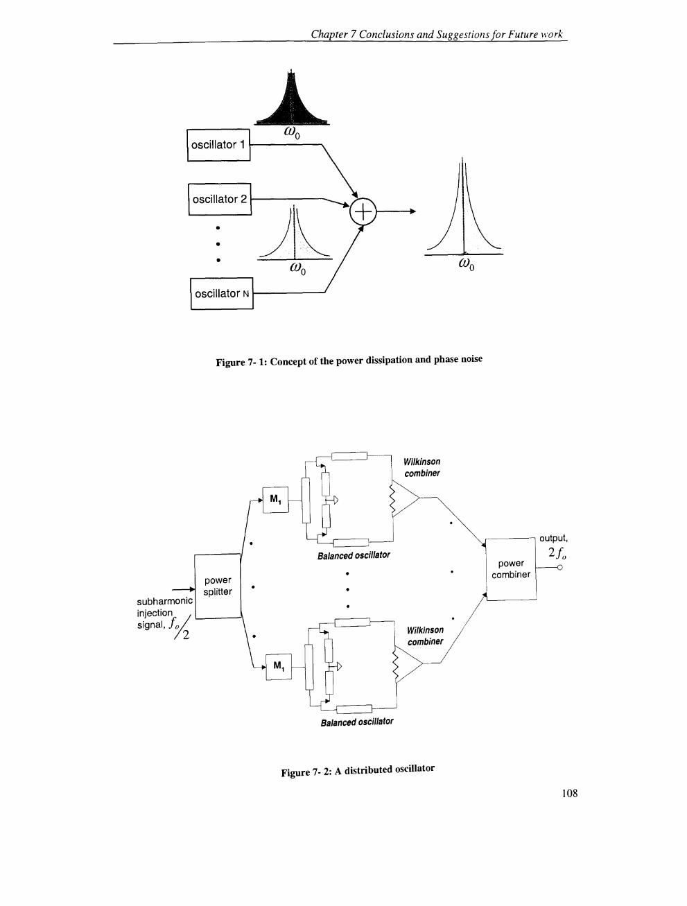
Chapter 7 Conclusions and Suggestions for Future work
0)0 oscillator 1 .......-----
\ oscillator 2\1-------• • •
oscillator N !--____ ...J
Figure 7- 1: Concept of the power dissipation and phase noise
subharmonic
injection~ signal, fo
2
power splitter •
Balanced oscillator
•
• •
Balanced oscillator
Wilkinson combiner
Wilkinson combiner
Figure 7- 2: A distributed oscillator
,--------, output,
power combiner
2fo
108

Chapter 7 Conclusions and Suggestions for Future )'.·ork
The other possible idea is to eliminate the unwanted signals in the frequency doubler. By
extending the work in chapter 6, this could be done by using the feedforward technique.
Referring to figure 6-14, the second loop, known as the error loop, is introduced. Here,
the error amplifier will produce a signal which is rich in odd harmonic components. For
the correct magnitude and phase, the signals from the first loop and the output of the error
amplifier at the second loop will be subtracted, resulting in the odd harmonic component
cancellation. However, the output can be degraded due the loss in the passive elements in
the circuit.
109

References
References
[1] M.K.Nezami, "Evaluate The Impact Of Phase Noise On Receiver Performance Phase
noise analysis, Part I", Microwave&RF Journal, pp.165-172, May 1998
[2] B.Petrovic, "A Balanced RF Oscillator", RF Design, pp. 35-38, December 1989
[3] J.Millman and C.C.Halkias, " INTEGRATED ELECTRONICS: ANALOG AND
DIGITAL CIRCUITS AND SYSTEMS", McGRAW-HILL, Inc., 1972
[4] G.Gonzales, "Microwave Transistor Amplifier Analysis and Design", 2nd edition,
1996
[5] LD.Robertson, "MMIC Design", The institution of Electrical Engineer, London UK,
1995
[6] A.Mortazawi, and B.C.De Loach, Jr., "Spatial Power Combining Oscillators Based on
Extended Resonance Technique", IEEE Transactions on Microwave Theory and
Techniques, vol. 42, No. 12, pp.2222-2228, December 1994
[7] K.S.Ang, S.Nam, and LD.Robertson, "A Balanced Monolithic Oscillator at K-Band",
IEEE Radio Frequency Integrated Circuits (RFIC) Symposium, pp.163, 1999
[8] R.E.Collin, "Foundations of Microwave engineering", 2nd edition, McGraw-Hill, 1992
[9] S.A.Maas, "Nonlinear Microwave Circuits", Arttech House Inc., 1988
[10] LD.Robertson, and S.Lucyszyn, "RFIC and MMIC design and technology", The
Institution of Electrical Engineer, chapter 6 Oscillators, K.K.M.Cheng, pp. 257-276,
London, UK, 2001
[11] S.A. Maas, "Microwave Mixers", 2nd edition, Arttech House Inc., 1993
[12] V.D.Hwang and T.Itoh , "A Quasi-Optical HEMT Self-Oscillating Mixer", pp.1093-
1096, IEEE Int' MTT-s Digest, 1988
[13] X.Zhou and A.S.Daryoush, "A Push-pull Self-oscillating mixer for optically FED
Phased Array", IEEE Int' MTT-s Digest, pp.321-324, 1993
110

References
[14] X.Zhou, and A.S.Daryoush, "An efficient self-oscillating mixer for communication",
IEEE Transactions on Microwave Theory and Techniques, vo1.42, pp.1858-1862,
October 1994
[15] X.Zhou, X.Zhang, and A.S.Daryoush, "A New Approach for a Phase Controlled
Self-oscillating Mixer", IEEE Transactions on Microwave Theory and Techniques.
vol.45, pp.196-204, February 1997
[16] C.M.Montiel, L.Fan, and K.Chang, "An X-Band Self-Mixing Oscillator Antenna for
Transceiver and Spiral Power-Combining Applications", IEEE Transactions on
Microwave Theory and Techniques, vol.46, pp.1546-1551, October 1998
[17] MJ.Roberts, S.Iezekiel, and C.M.Snowden, "A W -Band Self-Oscillating
Subharmonic MMIC Mixer", IEEE Transactions on Microwave Theory and
Techniques, vol. 12, pp.2104-2108, December 1998
[18] M.Claassen, and U.Guttich, "Conversion Matrix and Gain of Self-Oscillating
Mixers", IEEE Transactions on Microwave Theory and Techniques, vol.1, pp.25-30,
January 1991.
[19] K.Kamozaki, N.Kurita, T.Tanimoto, H.Ohta, T.Nakamura, and H.Kondoh, "50-100
GHz Octave Band MMIC Mixers", IEEE Radio Frequency Integrated Circuit
Symposium, pp.95-98, 1997
[20] R.Adler, " A Study of Locking Phenomena in Oscillators", Proceedings of the 1.R.E.
and Waves and Electrons, pp.351-357, June 1946.
[21] K.Kurokawa, " Noise in Synchronized Oscillators", IEEE Transactions on
Microwave Theory and Techniques, vol. MTT-16, No.4, pp.234-240, April 1968
[22] K.Kurokawa, " Injection Locking of Microwave Solid-State Oscillators",
Proceedings of the IEEE, vol. 61, No. 10, pp. 1386-1410, October 1973
[23] A.S.Daryoush, "Optical synchronization of millimeter wave oscillator for distributed
architecture (invited paper), IEEE Transactions on Microwave Theory and
Techniques, vol. 38, pp.467-476, May 1990
[24] A.S Daryoush, "Comparison of Indirect Optical Injection-locking Technique of
Multiple X-band Oscillators," IEEE Trans. Microwave Theory and Techniques. MTT-
34, vol. 12, pp. 1363-1370, December 1986
111

References
[25] J.Birkeland, T. Itoh, "Spatial Power Combining Using Push-Pull PET Oscillators
with Microstrip Patch Resonators", International Microwave Symposium Digest, pp.
1217-1219, 1990
[26] X.Zhou and A.S.Daryoush, "An Injection Locked Push-Pull Oscillator at Ku-Band".
IEEE Microwave and Guide Wave Letters, Vol.3, No.8, August 1993
[27] J.Birekeland and TatsuoItah, " A 16 Elementary Quasi-Optical PET Oscillator Power
Combining Array with External Injection Locking", IEEE Transactions on
Microwave Theory and Techniques, vol. 40, No.3, ppA75-481, March 1992
[28] X.zhang, X.Zhou and A.S.Daryoush, "A Theoretical Study of the Noise Behavior of
Subharmonically Injection Locked Oscillator", IEEE Transactions on Microwave
Theory and Techniques, vol. 40, No.5, pp.895-902, May 1992
[29] X.Zhang, X.Zhou, B.Aliener and A.S.Daryoush, "A Study of Subharmonic Injection
Locking for Local Oscillators", IEEE Transactions on Microwave Theory and
Techniques, vol. 2, No.3, pp.97-99, March 1992
[30] P.R.Herczfeld, A.S.Daryoush, A.Rosen, A.K.Sharma and V.M.Contarino, " Indirect
Subharmonic Optical Injection Locking of a Millimeter-Wave IMPATT Oscillator",
IEEE Transactions on Microwave Theory and Techniques, vol. MTT-34, No.12,
pp.1371-1375, December 1986
[31] C-C.Huang and T-H.Chu, " Analysis of MESFET Injection-Locked Oscillator in
Fundamental Mode of Operation", IEEE Transactions on Microwave Theory and
Techniques, vol.42, No.10, pp.1851-1857, October 1994
[32] H.P.Moyer and A.S.Daryoush, " A Unified Analytical Model and Experimental
Validations of Injection-locking Processes", IEEE Transactions on Microwave Theory
and Techniques, vol.48, NoA, ppA93-499, April 2000
[33] M.E.Hines, J-C.R.Collinet and lG.Ondria, " PM Noise Suppression of an Injection
Phase-Locked Oscillator", IEEE Transactions on Microwave Theory and Techniques,
vol. MTT-16, No.9, pp.738-742, September 1968
[34] M.Odyniec, "Nonlinear Synchrnized LC Oscillators: Theory and Simulation", IEEE
Transactions on Microwave Theory and Techniques, vol. 41, No.5, pp.77..t-780, May
1993
112

References
[35] K.F.Schtinemann and K.Behm, "Nonlinear Noise Theory for Synchnized
Oscillators", IEEE Transactions on Microwave Theory and Techniques, vol. MTT-27.
No.5, pp.452-458, May 1979
[36] A.P.S.Khanna, " Direct Measurement of the Nonlinear M.Le. Oscillator
Characteristics Using Injection Locking Polar Diagram", 1983 IEEE MTT-S ITIt.
Microwave Symp. Dig., pp. 501-503, 1983
[37] G.H.Bertil Hansson and K.Ingemar Lundstrom, " Stability Criteria for Phase-Locked
Oscillators", IEEE Transactions on Microwave Theory and Techniques, vol. MIT-20,
No.10, pp.641-645, October 1972
[38] D.Sommer and N.J.Gomes, "Wide-Locking Bandwidth Optically Injection-Locked
Oscillators: S-Parameter Design and Modulation Effects", IEEE Transactions on
Microwave Theory and Techniques, vol. 43, No.7, pp.1424-1432, July 1995
[39] J.Troger, P.-A.Nicati, L.Th6venaz, and Ph.A.Robert, " Novel Measurement Scheme
for Injection-Locking Experiments", IEEE journal of Quantum Electronics, vol. 35,
No.1, pp.32-38, January 1999
[40] B.Razavi, "RF Microelectronics", Prentice Hall, Inc., pp. 314-315,1998
[41] L.R.Malling, "Phase-Stable Oscillators for Space Communications, Including the
Relationship Between the Phase Noise, the Spectrum, the Short-Term Stability, and
the Q of the Oscillator", PROCEEDINGS OF THE IRE, pp.1656-1664, July 1962
[42] J.Meluin, "Background Noise in Nonlinear Oscillators", PROCEEDINGS OF THE
IRE, pp.1960-1473, August 1960
[43] C.Schiebold, "Getting Back to the Basics of Oscillator Design", Microwave Journal,
pp.336-339, May 1998
[44] H.E.Ott, "Noise Reduction Techniques in Electronic Systems", Wiley-Interscience
Publication, 1976.
[45] J.G.Ondria, "A Microwave System for Measurements of AM and PM noise Spectra",
IEEE Transactions on Microwave Theory and Techniques, vol. MIT-16, No.9, pp.
767-781, September 1968.
113

References
[46] H.C.Chang, X.Cao, U.K.Mishra and R.A.York, "Phase Noise in Coupled Oscillators:
Theory and Experiments", IEEE Transactions on Microwave Theory and Techniques,
vol. 45, No.5, pp.604-615, May 1997
[47] D.Schere, "Today's Leeson-Learn About Low-Noise Design Microwave, Part I",
Microwave Journal, pp.l16-122, April 1979
[48] G.D.Vendelin, A.M.Pavio, and U.L.Rhode, "Mirowave Circuit Design Using Linear
and Nonlinear Techniques", pp.418-437, New York, Chichester:Wiley, 1990
[49] M.Underhill, "Fundamantals of oscillator performance", Electronics &
Communication Engineering Journal, pp.185-193, August 1992
[50] S.Mizushina, "Corporate and Tandem Structures for Combining Power from 3N and
2N+1 Oscillators", IEEE Transactions on Microwave Theory and Techniques, vol.
MIT-28, No. 12, pp. 1428-1432, December 1980.
[51] M.Madihian and S.Mizushina, "Combining the Powers from Multiple-Device
Oscillators", IEEE Transactions on Microwave Theory and Techniques, vol. MTI-30,
No.8, pp. 1228-1233, August 1982.
[52] K.Chang and C.Sun, "Millimeter-Wave Power-Combining Techniques", IEEE
Transactions on Microwave Theory and Techniques, vol. MTI-31, No.2, pp. 91-107,
February 1983.
[53] S.Kudszus, T.Berceli, A.Tessmann, M.Neumann and W.H.Haydl, "W-Band HEMT
Oscillator MMICs Using Suharmonic Injection Locking", IEEE Transactions on
Microwave Theory and Techniques, vol. MIT 48, No. 12, pp. 2526-2532, December
2000
[54] R.Gilmore, " Concepts in the Design of Frequency Multipliers", Microwave Journal,
pp.129-139, March 1987
[55] C.Rauscher, "Frequency Doublers with GaAs PET's", 1982 IEEE MTJ-S Int.
Microwave Symp. Dig., pp. 280-282, 1982
[56] C.Rauscher, "High-Frequency Doubler Operation of GaAs Field-Effect Transistors",
1983 IEEE Transactions on Microwave Theory and Techniques, vol. MTI-31, pp.
462-472, June 1983
ll-l
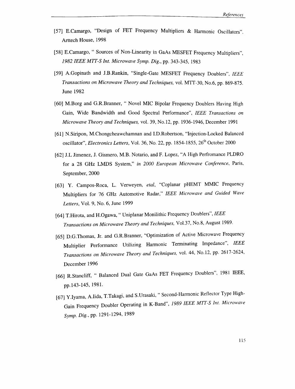
References
[57] E.Camargo, "Design of FET Frequency Multipliers & Harmonic Oscillators".
Arttech House, 1998
[58] E.Camargo, " Sources of Non-Linearity in GaAs MESFET Frequency Multipliers",
1982 IEEE MTT-S Int. Microwave Symp. Dig., pp. 343-345, 1983
[59] A.Gopinath and J.B.Rankin, "Single-Gate MESFET Frequency Doublers", IEEE
Transactions on Microwave Theory and Techniques, vol. MTI-30, No.6, pp. 869-875.
June 1982
[60] M.Borg and G.R.Branner, " Novel MIC Bipolar Frequency Doublers Having High
Gain, Wide Bandwidth and Good Spectral Performance", IEEE Transactions on
Microwave Theory and Techniques, vol. 39, No.12, pp. 1936-1946, December 1991
[61] N.Siripon, M.Chongcheawchamnan and LD.Robertson, "Injection-Locked Balanced
oscillator", Electronics Letters, Vol. 36, No. 22, pp. 1854-1855, 26th October 2000
[62] J.L Jimenez, 1. Gismero, M.B. Notario, and F. Lopez, "A High Perfromance PLDRO
for a 28 GHz LMDS System," in 2000 European Microwave Conference, Paris,
September, 2000
[63] Y. Campos-Roca, L. Verweyen, etal, "Coplanar pHEMT MMIC Frequency
Multipliers for 76 GHz Automotive Radar," IEEE Microwave and Guided Wave
Letters, Vol. 9, No.6, June 1999
[64] T.Hirota, and H.Ogawa, "Uniplanar Monilithic Frequency Doublers", IEEE
Transactions on Microwave Theory and Techniques, Vol.37, No.8, August 1989.
[65] D.G.Thomas, Jr. and G.R.Branner, "Optimization of Active Microwave Frequency
Multiplier Performance Utilizing Harmonic Terminating Impedance", IEEE
Transactions on Microwave Theory and Techniques, vol. 44, No.12, pp. 2617-2624,
December 1996
[66] R.Stancliff, " Balanced Dual Gate GaAs FET Frequency Doublers", 1981 IEEE,
pp.143-145,1981.
[67] Y.Iyama, A.Iida, T.Takagi, and S.Urasaki, " Second-Harmonic Reflector Type High
Gain Frequency Doubler Operating in K-Band", 1989 IEEE MTT-S Int. Microwave
Symp. Dig., pp. 1291-1294, 1989
115
References
[68] D.G.Thomas, Jr. and G.R.Branner, " Single-ended HEMT Multiplier Design Using
Reflector Networks", IEEE Transactions on Microwave Theory and Techniques, vol.
49, No.5 pp. 990-993, May 2001
[69] H.A.Willing, C.Rauscher and P.D.Santis, "A Technique for Predicting Large-Signal
Performance of a GaAs MESFET", IEEE Transactions on Microwave Theory and
Techniques, vol. MTT-26, No.12, pp. 1017-1023, December 1978
[70] Y.Campos-Roca, L.Verweyen, M.Neumanm, M.Femandez, M.C.Curras-Francos ,
E.Sanchez-Sanchez, A.Htilsmann, and M.Schlechtweg, "Coplanr pHEMT MMIC
Frequency Multiplier for 76-GHz Automotive Radar", IEEE Transactions on
Microwave Theory and Techniques, vol. 9,No. 6, pp. 242-244, June 1999
[71] I.Angelov, H.zirath, N.Rorsman, and H.Gronqvist, "A Balanced millimeter wave
doubler based on pseudomorphic HEMTs", 1992 IEEE MTT-S Int. Microwave Symp.
Dig., pp. 353-356, 1992
[72] lGrajal, V.Krozer, E.Gonalez, F.Maladonado, and lGismero, "Modeling and
Design Aspects of Millimeter-Wave and Submillimeter-Wave Schottky Diode
Varactor Frequency Multipliers", IEEE Transactions on Microwave Theory and
Techniques, vol. 48, pp. 700-711, April 2000
[73] Y.K.G.Hau, V.Postoyalko, and J.R.Richardson, "Effect of impedance mismatch and
imperfect isolation on distortion cancellation in feedforward amplifiers", lEE Proc.
Circuits Devices Syst., vol. 145, pp. 35-39, February 1998
[74] Y.K.G.Hau, V.Postoyalko, and lR.Richardson, "Compensation of amplifier
nonlinear phase response to improve wideband distortion cancellation of feedforward
amplifiers", Electronics Letters., vol. 33, pp. 500-502, March 1997
[75] S.Kang, I.Lee and K.S.Yoo, " Analysis and Design of the Feedforward Power
Amplifier", 1997 IEEE MTT-S Int. Microwave Symp. Dig., pp. 1519-1522, 1997.
[76] C.McNeilage, E.N.Ivanov, P.R. Stockwell, and J.R.Searls, "Review of Feedback and
Feedforward Noise Reduction Techniques", 1998 IEEE International Frequency
Control Symp., pp.146-153, 1998
[77] N.Pothecary, "Feedforward Linear Power Amplifier", Artech House, Inc .. 1999
[78] J.Hogerheiden, M.Cimihera, and GJue, "Improved Planar Spiral Transformer
Theory Applied to a Muniature Lumped Element Quadrature Hybrid", IEEE
116

References
Transactions on Microwave Theory and Techniques, vol. 45,No. 4, pp. 462-472,
April, 1997
[79] N.Siripon, K.S.Ang, M.Chongcheawchamnan and I.D.Robertson, "Design and
Performance of a novel balanced self-oscillating mixer", 3rJh European Microwave
Con!, Paris, France, 2-6 October 2000
[80] N.Siripon, M.Chongcheawchamnan and I.D.Robertson, "Novel Sub-hannonic
Injection-Locked Balanced Oscillator", 3th European Microwave Conj, London,
UK, 24-28 September 2001
[81] N.Siripon, M.Chongcheawchamnan and I.D.Robertson, "Novel Frequency Doubler
using Feedforward for Fundamnetla Frequency Component Suppression", 2001 IEEE
Microwave MTT-S Int. Symp. Dig., Phoenix, Arozona, 20-25 May 2001
[82] M.J.Underhill, N.Siripon and N.Christorou, "Determination of Capture Range and
Locking Range of Injection Locked Oscillators", 15th European Frequency and Time
Forum, Switzerland, March 2001
[83] M.J.Underhill and N.Siripon, "AN INVESTIGATION OF A CASCADED PAIR OF
INJECTION-LOCKED OSCILLATORS AT 2GHz", 16th European Frequency and
Time Forum, Switzerland, March 2002
[84] N.Siripon, M.Chongcheawchamnan and I.D.Robertson, "Injection-Locked Balanced
oscillator-Doubler", lEE Electronic Letters, Vol. 37, No. 15, pp. 958-959, 19th
July
2001.
[85] A.V.Derziel, "Noise", Prentice-Hall Electronical Engineering Series, pp. 1-7,
Prentice-Hall, Inc., 1956
117


![Untitled-1 [newport.eecs.uci.edu]newport.eecs.uci.edu/rfmems/publications/papers/others/C037.pdfmicrowave design, specifically, microwave impedance matching [4] and antenna design](https://img.dokumen.tips/doc/110x75/5e9ac58659dc026b0672dc64/untitled-1-microwave-design-specifically-microwave-impedance-matching-4.jpg)


