Embed Size (px)
Citation preview

DATA SHEET
Product specificationSupersedes data of 2000 Feb 07
2000 Jul 31
INTEGRATED CIRCUITS
UDA1334BTSLow power audio DAC
NXP Semiconductors Product specification
Low power audio DAC UDA1334BTS
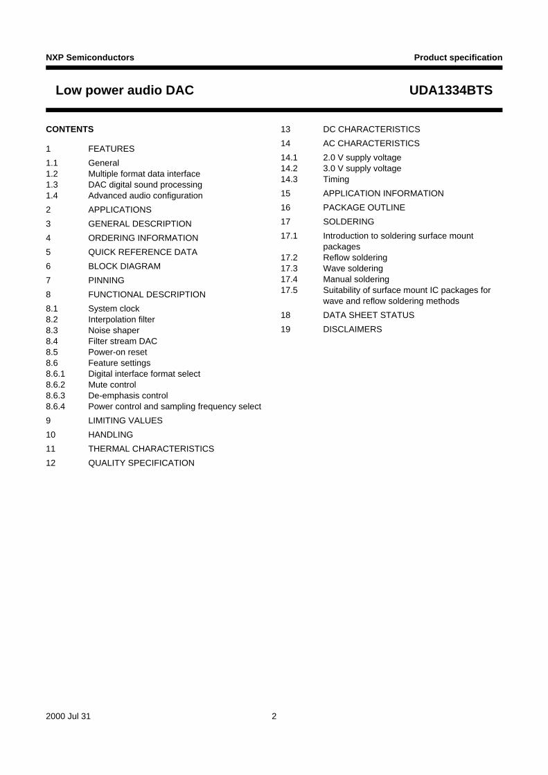
CONTENTS
1 FEATURES1.1 General1.2 Multiple format data interface1.3 DAC digital sound processing1.4 Advanced audio configuration2 APPLICATIONS3 GENERAL DESCRIPTION4 ORDERING INFORMATION5 QUICK REFERENCE DATA6 BLOCK DIAGRAM7 PINNING8 FUNCTIONAL DESCRIPTION8.1 System clock8.2 Interpolation filter8.3 Noise shaper8.4 Filter stream DAC8.5 Power-on reset8.6 Feature settings8.6.1 Digital interface format select8.6.2 Mute control8.6.3 De-emphasis control8.6.4 Power control and sampling frequency select9 LIMITING VALUES10 HANDLING11 THERMAL CHARACTERISTICS12 QUALITY SPECIFICATION
13 DC CHARACTERISTICS14 AC CHARACTERISTICS14.1 2.0 V supply voltage14.2 3.0 V supply voltage14.3 Timing15 APPLICATION INFORMATION16 PACKAGE OUTLINE17 SOLDERING17.1 Introduction to soldering surface mount
packages17.2 Reflow soldering17.3 Wave soldering17.4 Manual soldering17.5 Suitability of surface mount IC packages for
wave and reflow soldering methods18 DATA SHEET STATUS19 DISCLAIMERS
2000 Jul 31 2
NXP Semiconductors Product specification
Low power audio DAC UDA1334BTS
1 FEATURES
1.1 General
• 1.8 to 3.6 V power supply voltage• Integrated digital filter plus DAC• Supports sample frequencies from 8 to 100 kHz• Automatic system clock versus sample rate detection• Low power consumption• No analog post filtering required for DAC• Slave mode only applications• Easy application• SSOP16 package.
1.2 Multiple format data interface
• I2S-bus and LSB-justified format compatible• 1fs input data rate.
1.3 DAC digital sound processing
• Digital de-emphasis for 44.1 kHz sampling rate• Mute function.
1.4 Advanced audio configuration
• High linearity, wide dynamic range and low distortion• Standby or Sleep mode in which the DAC is powered
down.
2 APPLICATIONS
This audio DAC is excellently suitable for digital audio portable application, such as portable MD, MP3 and DVD players.
3 GENERAL DESCRIPTION
The UDA1334BTS supports the I2S-bus data format with word lengths of up to 24 bits and the LSB-justified serial data format with word lengths of 16, 20 and 24 bits.
The UDA1334BTS has basic features such as de-emphasis (at 44.1 kHz sampling rate) and mute.
4 ORDERING INFORMATION
TYPE NUMBER
PACKAGE
NAME DESCRIPTION VERSIONUDA1334BTS SSOP16 plastic shrink small outline package; 16 leads; body width 4.4 mm SOT369-1
2000 Jul 31 3
NXP Semiconductors Product specification
Low power audio DAC UDA1334BTS
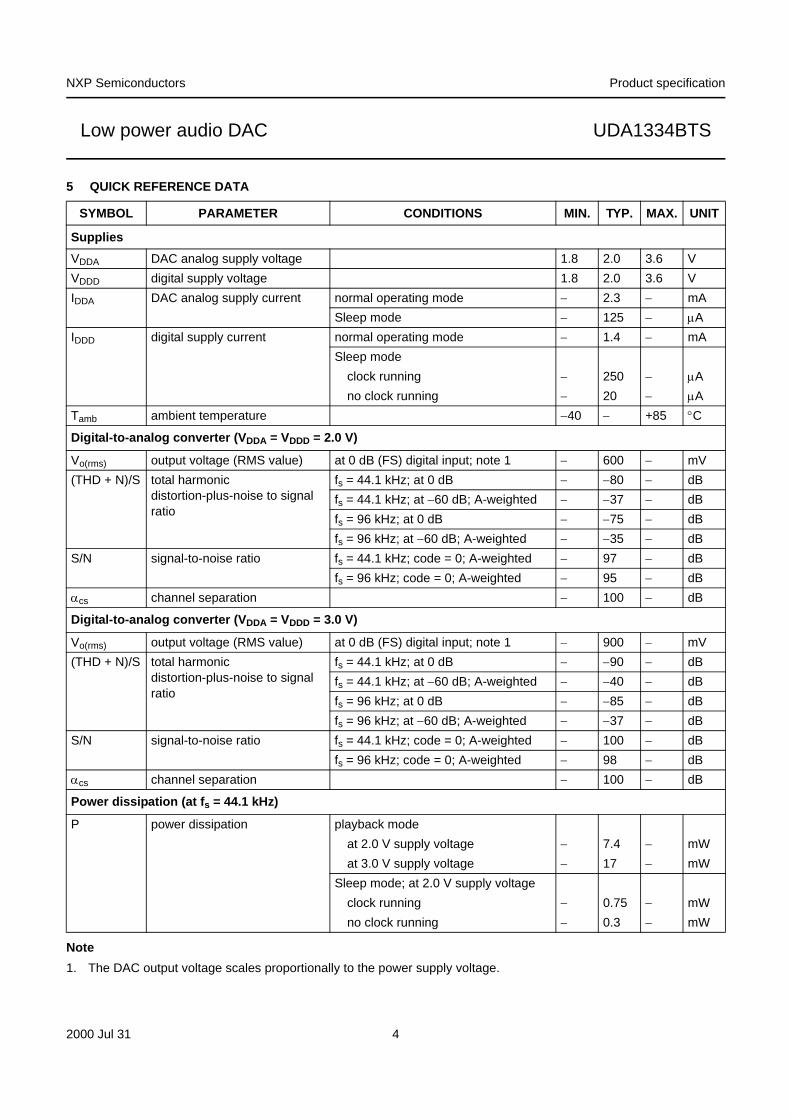
5 QUICK REFERENCE DATA
Note1. The DAC output voltage scales proportionally to the power supply voltage.
SYMBOL PARAMETER CONDITIONS MIN. TYP. MAX. UNIT
SuppliesVDDA DAC analog supply voltage 1.8 2.0 3.6 VVDDD digital supply voltage 1.8 2.0 3.6 VIDDA DAC analog supply current normal operating mode − 2.3 − mA
Sleep mode − 125 − μAIDDD digital supply current normal operating mode − 1.4 − mA
Sleep modeclock running − 250 − μAno clock running − 20 − μA
Tamb ambient temperature −40 − +85 °C
Digital-to-analog converter (VDDA = VDDD = 2.0 V)
Vo(rms) output voltage (RMS value) at 0 dB (FS) digital input; note 1 − 600 − mV(THD + N)/S total harmonic
distortion-plus-noise to signal ratio
fs = 44.1 kHz; at 0 dB − −80 − dBfs = 44.1 kHz; at −60 dB; A-weighted − −37 − dBfs = 96 kHz; at 0 dB − −75 − dBfs = 96 kHz; at −60 dB; A-weighted − −35 − dB
S/N signal-to-noise ratio fs = 44.1 kHz; code = 0; A-weighted − 97 − dBfs = 96 kHz; code = 0; A-weighted − 95 − dB
αcs channel separation − 100 − dB
Digital-to-analog converter (VDDA = VDDD = 3.0 V)
Vo(rms) output voltage (RMS value) at 0 dB (FS) digital input; note 1 − 900 − mV(THD + N)/S total harmonic
distortion-plus-noise to signal ratio
fs = 44.1 kHz; at 0 dB − −90 − dBfs = 44.1 kHz; at −60 dB; A-weighted − −40 − dBfs = 96 kHz; at 0 dB − −85 − dBfs = 96 kHz; at −60 dB; A-weighted − −37 − dB
S/N signal-to-noise ratio fs = 44.1 kHz; code = 0; A-weighted − 100 − dBfs = 96 kHz; code = 0; A-weighted − 98 − dB
αcs channel separation − 100 − dB
Power dissipation (at fs = 44.1 kHz)
P power dissipation playback modeat 2.0 V supply voltage − 7.4 − mWat 3.0 V supply voltage − 17 − mW
Sleep mode; at 2.0 V supply voltageclock running − 0.75 − mWno clock running − 0.3 − mW
2000 Jul 31 4

NXP Semiconductors Product specification
Low power audio DAC UDA1334BTS
6 BLOCK DIAGRAM
handbook, full pagewidth
MGL964
DAC
UDA1334BTS
NOISE SHAPER
INTERPOLATION FILTER
DE-EMPHASIS
14
15
DAC
6
DIGITAL INTERFACE
16
321
4 5
11
7
13 12
VOUTR
BCK
VSSA
WS
VOUTL
DATAI
VDDA
VDDD
Vref(DAC)
VSSD
SFOR0
SYSCLK8
MUTE9
DEEM10
PCS
SFOR1
Fig.1 Block diagram.
2000 Jul 31 5
NXP Semiconductors Product specification
Low power audio DAC UDA1334BTS
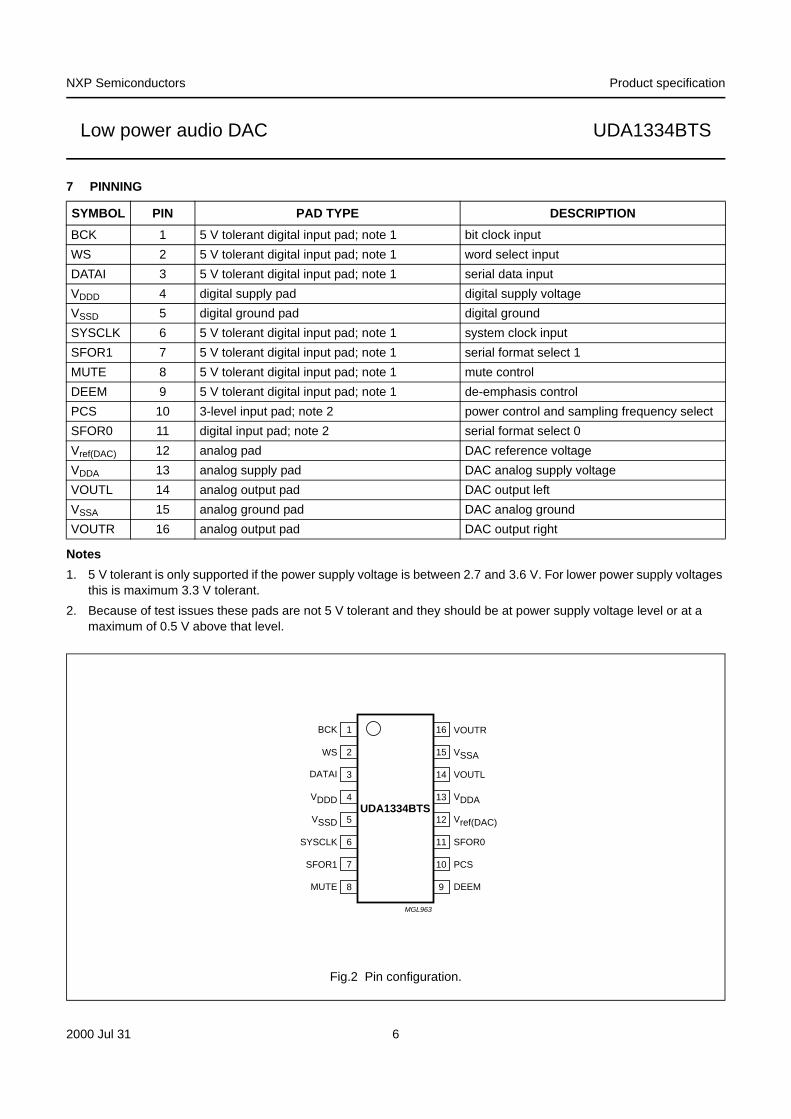
7 PINNING
Notes1. 5 V tolerant is only supported if the power supply voltage is between 2.7 and 3.6 V. For lower power supply voltages
this is maximum 3.3 V tolerant.2. Because of test issues these pads are not 5 V tolerant and they should be at power supply voltage level or at a
maximum of 0.5 V above that level.
SYMBOL PIN PAD TYPE DESCRIPTIONBCK 1 5 V tolerant digital input pad; note 1 bit clock inputWS 2 5 V tolerant digital input pad; note 1 word select inputDATAI 3 5 V tolerant digital input pad; note 1 serial data inputVDDD 4 digital supply pad digital supply voltageVSSD 5 digital ground pad digital groundSYSCLK 6 5 V tolerant digital input pad; note 1 system clock inputSFOR1 7 5 V tolerant digital input pad; note 1 serial format select 1MUTE 8 5 V tolerant digital input pad; note 1 mute controlDEEM 9 5 V tolerant digital input pad; note 1 de-emphasis controlPCS 10 3-level input pad; note 2 power control and sampling frequency selectSFOR0 11 digital input pad; note 2 serial format select 0Vref(DAC) 12 analog pad DAC reference voltageVDDA 13 analog supply pad DAC analog supply voltageVOUTL 14 analog output pad DAC output leftVSSA 15 analog ground pad DAC analog groundVOUTR 16 analog output pad DAC output right
handbook, halfpage
UDA1334BTS
MGL963
1
2
3
4
5
6
7
8
16
15
14
13
12
11
10
9
VOUTRBCK
VSSAWS
VOUTLDATAI
VDDAVDDD
Vref(DAC)VSSD
SFOR0SYSCLK
PCSSFOR1
DEEMMUTE
Fig.2 Pin configuration.
2000 Jul 31 6
NXP Semiconductors Product specification
Low power audio DAC UDA1334BTS
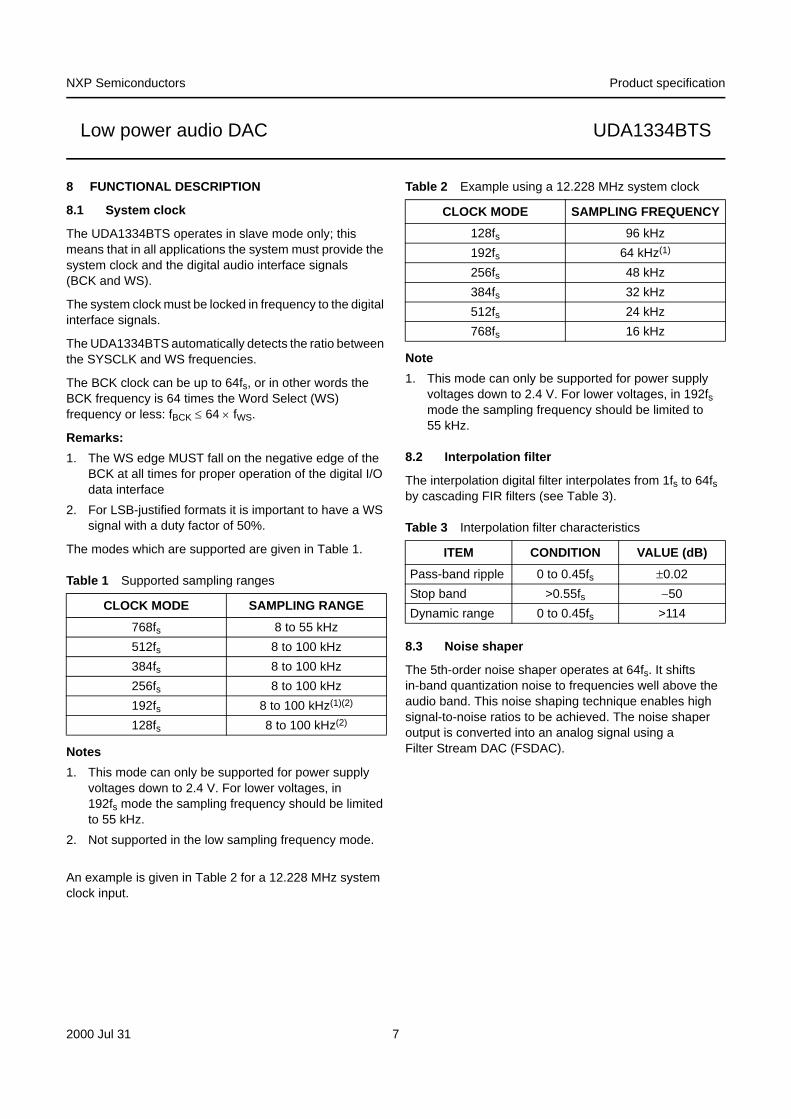
8 FUNCTIONAL DESCRIPTION
8.1 System clock
The UDA1334BTS operates in slave mode only; this means that in all applications the system must provide the system clock and the digital audio interface signals (BCK and WS).
The system clock must be locked in frequency to the digital interface signals.
The UDA1334BTS automatically detects the ratio between the SYSCLK and WS frequencies.
The BCK clock can be up to 64fs, or in other words the BCK frequency is 64 times the Word Select (WS) frequency or less: fBCK ≤ 64 × fWS.
Remarks:1. The WS edge MUST fall on the negative edge of the
BCK at all times for proper operation of the digital I/O data interface
2. For LSB-justified formats it is important to have a WS signal with a duty factor of 50%.
The modes which are supported are given in Table 1.
Table 1 Supported sampling ranges
Notes1. This mode can only be supported for power supply
voltages down to 2.4 V. For lower voltages, in 192fs mode the sampling frequency should be limited to 55 kHz.
2. Not supported in the low sampling frequency mode.
An example is given in Table 2 for a 12.228 MHz system clock input.
Table 2 Example using a 12.228 MHz system clock
Note1. This mode can only be supported for power supply
voltages down to 2.4 V. For lower voltages, in 192fs mode the sampling frequency should be limited to 55 kHz.
8.2 Interpolation filter
The interpolation digital filter interpolates from 1fs to 64fs by cascading FIR filters (see Table 3).
Table 3 Interpolation filter characteristics
8.3 Noise shaper
The 5th-order noise shaper operates at 64fs. It shifts in-band quantization noise to frequencies well above the audio band. This noise shaping technique enables high signal-to-noise ratios to be achieved. The noise shaper output is converted into an analog signal using a Filter Stream DAC (FSDAC).
CLOCK MODE SAMPLING RANGE768fs 8 to 55 kHz512fs 8 to 100 kHz384fs 8 to 100 kHz256fs 8 to 100 kHz192fs 8 to 100 kHz(1)(2)
128fs 8 to 100 kHz(2)
CLOCK MODE SAMPLING FREQUENCY128fs 96 kHz192fs 64 kHz(1)
256fs 48 kHz384fs 32 kHz512fs 24 kHz768fs 16 kHz
ITEM CONDITION VALUE (dB)Pass-band ripple 0 to 0.45fs ±0.02Stop band >0.55fs −50Dynamic range 0 to 0.45fs >114
2000 Jul 31 7
NXP Semiconductors Product specification
Low power audio DAC UDA1334BTS
8.4 Filter stream DAC
The FSDAC is a semi-digital reconstruction filter that converts the 1-bit data stream of the noise shaper to an analog output voltage. The filter coefficients are implemented as current sources and are summed at virtual ground of the output operational amplifier. In this way very high signal-to-noise performance and low clock jitter sensitivity is achieved. No post-filter is needed due to the inherent filter function of the DAC. On-board amplifiers convert the FSDAC output current to an output voltage signal capable of driving a line output.
The output voltage of the FSDAC scales proportionally with the power supply voltage.
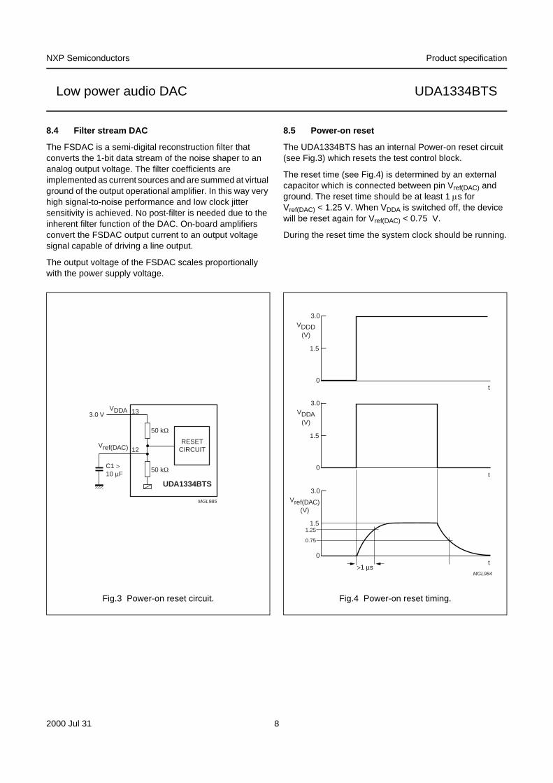
8.5 Power-on reset
The UDA1334BTS has an internal Power-on reset circuit (see Fig.3) which resets the test control block.
The reset time (see Fig.4) is determined by an external capacitor which is connected between pin Vref(DAC) and ground. The reset time should be at least 1 μs for Vref(DAC) < 1.25 V. When VDDA is switched off, the device will be reset again for Vref(DAC) < 0.75 V.
During the reset time the system clock should be running.
handbook, halfpage VDDA
Vref(DAC)
3.0 V 13
12
MGL985
UDA1334BTS
C1 >10 μF
RESETCIRCUIT
50 kΩ
50 kΩ
Fig.3 Power-on reset circuit.
handbook, halfpage3.0
VDDD(V)
1.5
0t
3.0VDDA
(V)
1.5
0t
3.0Vref(DAC)
(V)
1.51.25
0.75
0t
MGL984>1 μs
Fig.4 Power-on reset timing.
2000 Jul 31 8
NXP Semiconductors Product specification
Low power audio DAC UDA1334BTS
8.6 Feature settings
The features of the UDA1334BTS can be set by control pins SFOR1, SFOR0, MUTE, DEEM and PCS.
8.6.1 DIGITAL INTERFACE FORMAT SELECT
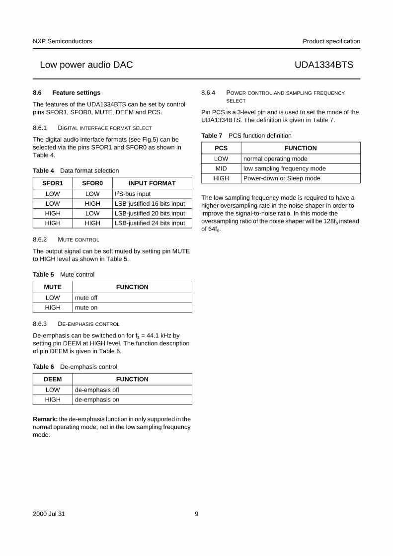
The digital audio interface formats (see Fig.5) can be selected via the pins SFOR1 and SFOR0 as shown in Table 4.
Table 4 Data format selection
8.6.2 MUTE CONTROL
The output signal can be soft muted by setting pin MUTE to HIGH level as shown in Table 5.
Table 5 Mute control
8.6.3 DE-EMPHASIS CONTROL
De-emphasis can be switched on for fs = 44.1 kHz by setting pin DEEM at HIGH level. The function description of pin DEEM is given in Table 6.
Table 6 De-emphasis control
Remark: the de-emphasis function in only supported in the normal operating mode, not in the low sampling frequency mode.
8.6.4 POWER CONTROL AND SAMPLING FREQUENCY SELECT
Pin PCS is a 3-level pin and is used to set the mode of the UDA1334BTS. The definition is given in Table 7.
Table 7 PCS function definition
The low sampling frequency mode is required to have a higher oversampling rate in the noise shaper in order to improve the signal-to-noise ratio. In this mode the oversampling ratio of the noise shaper will be 128fs instead of 64fs.
SFOR1 SFOR0 INPUT FORMATLOW LOW I2S-bus inputLOW HIGH LSB-justified 16 bits inputHIGH LOW LSB-justified 20 bits inputHIGH HIGH LSB-justified 24 bits input
MUTE FUNCTIONLOW mute offHIGH mute on
DEEM FUNCTIONLOW de-emphasis offHIGH de-emphasis on
PCS FUNCTIONLOW normal operating modeMID low sampling frequency mode
HIGH Power-down or Sleep mode
2000 Jul 31 9
2000Jul31
NX
P S
emiconductors
Product specification
Low pow
er audio DA
CU
DA
1334BTS
handbook, full pagewidth
MGS752
16
B8 B9 B10
158 17 2 1
B23 LSB
16
B4 B5 B6
158 17 2 1
B19 LSB
16
MSB B2
15 2 1
B15 LSB
10
16
B5 B6 B7 B8 B9 B10
LEFT
LSB-JUSTIFIED FORMAT 24 BITS
WS
BCK
DATA
RIGHT
1518 1720 1922 212324 2 1
B3 B4MSB B2 B23 LSB B5 B6 B7
120 1922 212324
B3 B4MSB B2
16
MSB B2 B3 B4 B5 B6
LEFT
LSB-JUSTIFIED FORMAT 20 BITS
WS
BCK
DATA
RIGHT
1518 1720 19 2 1
B19 LSB MSB B2 B3
120 19
16
MSB B2
LEFT
LSB-JUSTIFIED FORMAT 16 BITS
WS
BCK
DATA
RIGHT
15 2 1
B15 LSB
MSB MSBB2
21> = 81 2 3
LEFT
I2S-BUS FORMAT
WS
BCK
DATA
RIGHT
3 > = 8
MSB B2
Fig.5 Digital audio formats
NXP Semiconductors Product specification
Low power audio DAC UDA1334BTS
9 LIMITING VALUESIn accordance with the Absolute Maximum Rating System (IEC 60134).
Note1. All supply connections must be made to the same power supply.2. Short-circuit test at Tamb = 0 °C and VDDA = 3 V. DAC operation after short-circuiting cannot be warranted.
10 HANDLING
Inputs and outputs are protected against electrostatic discharge in normal handling. However, it is good practice to take normal precautions appropriate to handling MOS devices.
11 THERMAL CHARACTERISTICS
12 QUALITY SPECIFICATION
In accordance with “SNW-FQ-611-E”.
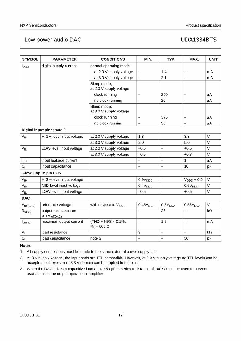
13 DC CHARACTERISTICSVDDD = VDDA = 2.0 V; Tamb = 25 °C; RL = 5 kΩ; all voltages with respect to ground (pins VSSA and VSSD); unless otherwise specified.
SYMBOL PARAMETER CONDITIONS MIN. MAX. UNITVDD supply voltage note 1 − 4.0 VTxtal(max) maximum crystal temperature − 150 °CTstg storage temperature −65 +125 °CTamb ambient temperature −40 +85 °CVes electrostatic handling voltage human body model −2000 +2000 V
machine model −200 +200 VIsc(DAC) short-circuit current of DAC note 2
output short-circuited to VSSA − 450 mAoutput short-circuited to VDDA − 300 mA
SYMBOL PARAMETER CONDITIONS VALUE UNITRth(j-a) thermal resistance from junction to ambient in free air 145 K/W
SYMBOL PARAMETER CONDITIONS MIN. TYP. MAX. UNIT
SuppliesVDDA DAC analog supply voltage note 1 1.8 2.0 3.6 VVDDD digital supply voltage note 1 1.8 2.0 3.6 VIDDA DAC analog supply current normal operating mode
at 2.0 V supply voltage − 2.3 − mAat 3.0 V supply voltage − 3.5 − mA
Sleep modeat 2.0 V supply voltage − 125 − μAat 3.0 V supply voltage − 175 − μA
2000 Jul 31 11
NXP Semiconductors Product specification
Low power audio DAC UDA1334BTS
Notes1. All supply connections must be made to the same external power supply unit.2. At 3 V supply voltage, the input pads are TTL compatible. However, at 2.0 V supply voltage no TTL levels can be
accepted, but levels from 3.3 V domain can be applied to the pins.3. When the DAC drives a capacitive load above 50 pF, a series resistance of 100 Ω must be used to prevent
oscillations in the output operational amplifier.
IDDD digital supply current normal operating modeat 2.0 V supply voltage − 1.4 − mAat 3.0 V supply voltage − 2.1 − mA
Sleep mode; at 2.0 V supply voltage
clock running − 250 − μAno clock running − 20 − μA
Sleep mode; at 3.0 V supply voltage
clock running − 375 − μAno clock running − 30 − μA
Digital input pins; note 2
VIH HIGH-level input voltage at 2.0 V supply voltage 1.3 − 3.3 Vat 3.0 V supply voltage 2.0 − 5.0 V
VIL LOW-level input voltage at 2.0 V supply voltage −0.5 − +0.5 Vat 3.0 V supply voltage −0.5 − +0.8 V
⎪ILI⎪ input leakage current − − 1 μACi input capacitance − − 10 pF
3-level input: pin PCSVIH HIGH-level input voltage 0.9VDDD − VDDD + 0.5 VVIM MID-level input voltage 0.4VDDD − 0.6VDDD VVIL LOW-level input voltage −0.5 − +0.5 V
DACVref(DAC) reference voltage with respect to VSSA 0.45VDDA 0.5VDDA 0.55VDDA VRo(ref) output resistance on
pin Vref(DAC)
− 25 − kΩ
Io(max) maximum output current (THD + N)/S < 0.1%; RL = 800 Ω
− 1.6 − mA
RL load resistance 3 − − kΩCL load capacitance note 3 − − 50 pF
SYMBOL PARAMETER CONDITIONS MIN. TYP. MAX. UNIT
2000 Jul 31 12
NXP Semiconductors Product specification
Low power audio DAC UDA1334BTS
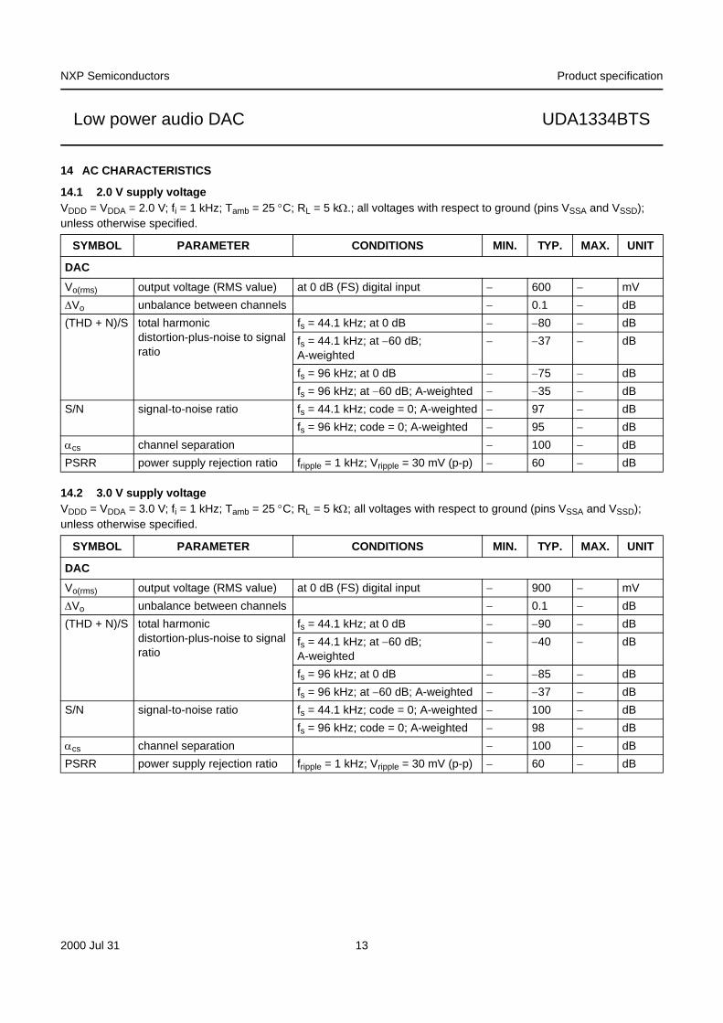
14 AC CHARACTERISTICS
14.1 2.0 V supply voltageVDDD = VDDA = 2.0 V; fi = 1 kHz; Tamb = 25 °C; RL = 5 kΩ.; all voltages with respect to ground (pins VSSA and VSSD); unless otherwise specified.
14.2 3.0 V supply voltageVDDD = VDDA = 3.0 V; fi = 1 kHz; Tamb = 25 °C; RL = 5 kΩ; all voltages with respect to ground (pins VSSA and VSSD); unless otherwise specified.
SYMBOL PARAMETER CONDITIONS MIN. TYP. MAX. UNIT
DACVo(rms) output voltage (RMS value) at 0 dB (FS) digital input − 600 − mVΔVo unbalance between channels − 0.1 − dB(THD + N)/S total harmonic
distortion-plus-noise to signal ratio
fs = 44.1 kHz; at 0 dB − −80 − dBfs = 44.1 kHz; at −60 dB; A-weighted
− −37 − dB
fs = 96 kHz; at 0 dB − −75 − dBfs = 96 kHz; at −60 dB; A-weighted − −35 − dB
S/N signal-to-noise ratio fs = 44.1 kHz; code = 0; A-weighted − 97 − dBfs = 96 kHz; code = 0; A-weighted − 95 − dB
αcs channel separation − 100 − dBPSRR power supply rejection ratio fripple = 1 kHz; Vripple = 30 mV (p-p) − 60 − dB
SYMBOL PARAMETER CONDITIONS MIN. TYP. MAX. UNIT
DACVo(rms) output voltage (RMS value) at 0 dB (FS) digital input − 900 − mVΔVo unbalance between channels − 0.1 − dB(THD + N)/S total harmonic
distortion-plus-noise to signal ratio
fs = 44.1 kHz; at 0 dB − −90 − dBfs = 44.1 kHz; at −60 dB; A-weighted
− −40 − dB
fs = 96 kHz; at 0 dB − −85 − dBfs = 96 kHz; at −60 dB; A-weighted − −37 − dB
S/N signal-to-noise ratio fs = 44.1 kHz; code = 0; A-weighted − 100 − dBfs = 96 kHz; code = 0; A-weighted − 98 − dB
αcs channel separation − 100 − dBPSRR power supply rejection ratio fripple = 1 kHz; Vripple = 30 mV (p-p) − 60 − dB
2000 Jul 31 13
NXP Semiconductors Product specification
Low power audio DAC UDA1334BTS
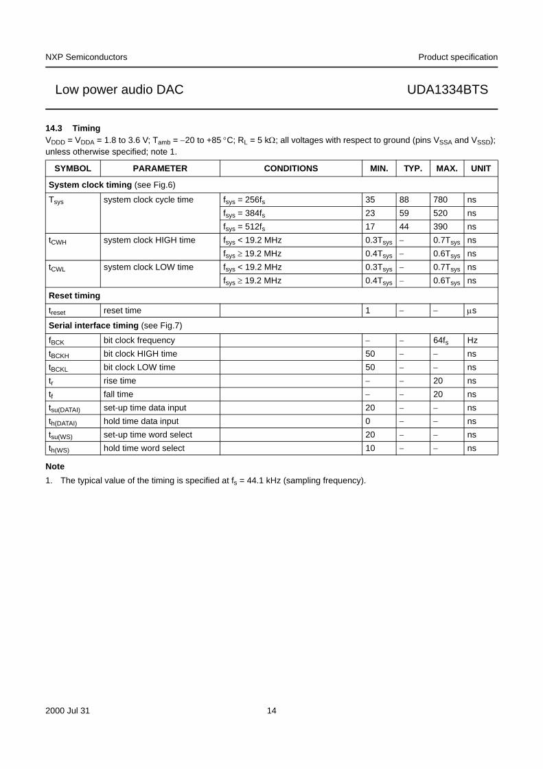
14.3 TimingVDDD = VDDA = 1.8 to 3.6 V; Tamb = −20 to +85 °C; RL = 5 kΩ; all voltages with respect to ground (pins VSSA and VSSD); unless otherwise specified; note 1.
Note1. The typical value of the timing is specified at fs = 44.1 kHz (sampling frequency).
SYMBOL PARAMETER CONDITIONS MIN. TYP. MAX. UNIT
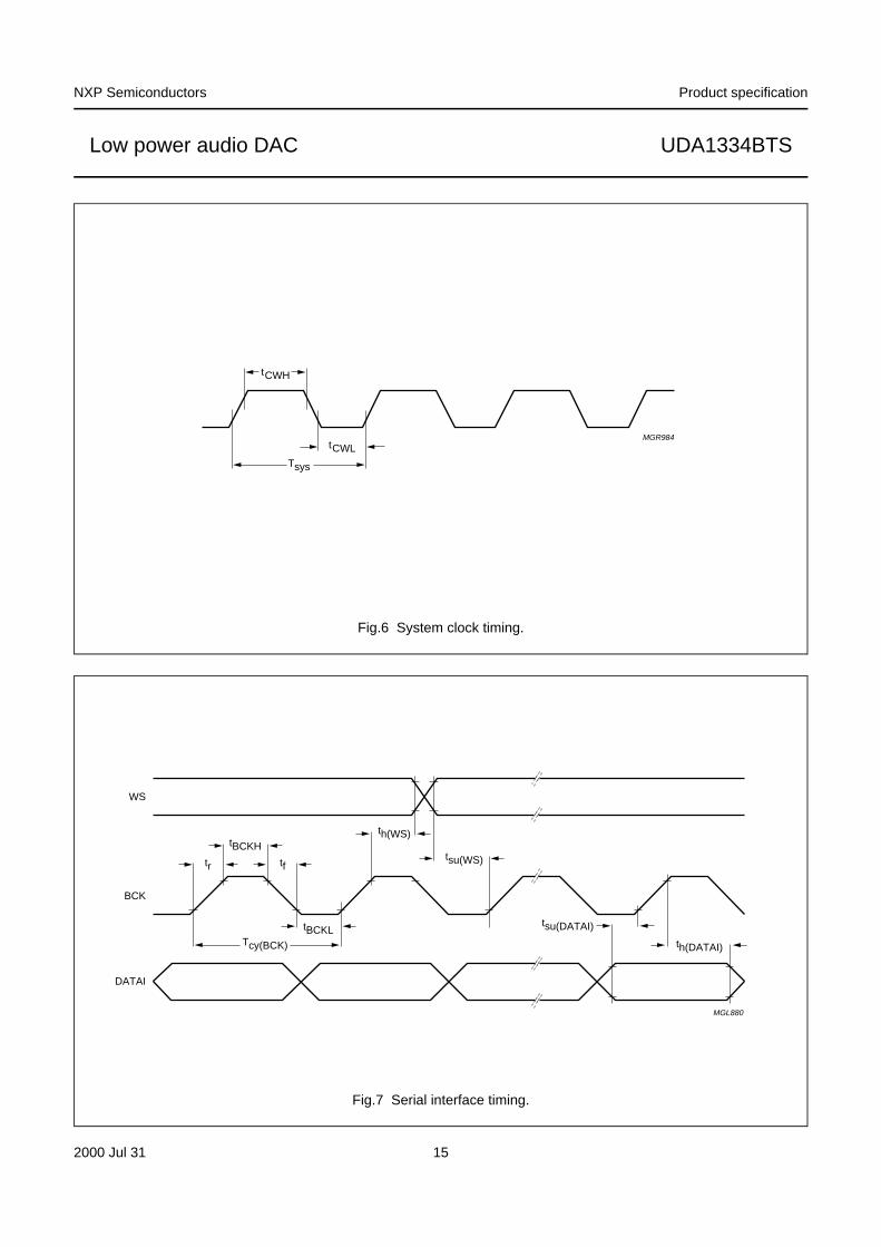
System clock timing (see Fig.6)
Tsys system clock cycle time fsys = 256fs 35 88 780 nsfsys = 384fs 23 59 520 nsfsys = 512fs 17 44 390 ns
tCWH system clock HIGH time fsys < 19.2 MHz 0.3Tsys − 0.7Tsys nsfsys ≥ 19.2 MHz 0.4Tsys − 0.6Tsys ns
tCWL system clock LOW time fsys < 19.2 MHz 0.3Tsys − 0.7Tsys nsfsys ≥ 19.2 MHz 0.4Tsys − 0.6Tsys ns
Reset timingtreset reset time 1 − − μs
Serial interface timing (see Fig.7)
fBCK bit clock frequency − − 64fs HztBCKH bit clock HIGH time 50 − − nstBCKL bit clock LOW time 50 − − nstr rise time − − 20 nstf fall time − − 20 nstsu(DATAI) set-up time data input 20 − − nsth(DATAI) hold time data input 0 − − nstsu(WS) set-up time word select 20 − − nsth(WS) hold time word select 10 − − ns
2000 Jul 31 14
NXP Semiconductors Product specification
Low power audio DAC UDA1334BTS
handbook, full pagewidth
MGR984
Tsys
tCWH
tCWL
Fig.6 System clock timing.
handbook, full pagewidth
MGL880
tf
th(WS)
tsu(WS)
tsu(DATAI)
th(DATAI)
tBCKH
tBCKLTcy(BCK)
tr
WS
BCK
DATAI
Fig.7 Serial interface timing.
2000 Jul 31 15
NXP Semiconductors Product specification
Low power audio DAC UDA1334BTS
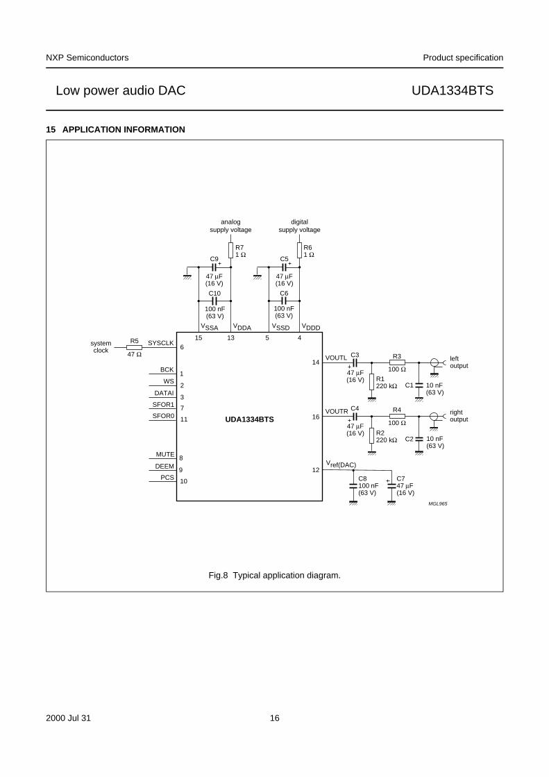
15 APPLICATION INFORMATION
handbook, full pagewidth
MGL965
47 Ω
R5
UDA1334BTS
6SYSCLKsystem
clock
1BCK
2WS
3DATAI
14VOUTL R3
100 ΩR1220 kΩ
16VOUTR R4
100 ΩR2220 kΩ
7SFOR1
11SFOR0
9DEEM
10PCS
8MUTE
47 μF(16 V)
C4
47 μF(16 V)
C3 leftoutput
rightoutput
12Vref(DAC)
C747 μF(16 V)
C8100 nF(63 V)
45
VDDDVSSD
R61 Ω
digitalsupply voltage
C6
15 13
VSSA VDDA
R71 Ω
C9
47 μF(16 V)
C10
100 nF(63 V)
100 nF(63 V)
analogsupply voltage
C5
47 μF(16 V)
C1 10 nF(63 V)
10 nF(63 V)
C2
Fig.8 Typical application diagram.
2000 Jul 31 16

NXP Semiconductors Product specification
Low power audio DAC UDA1334BTS
16 PACKAGE OUTLINE
UNIT A1 A2 A3 bp c D(1) E(1) (1)e HE L Lp Q Zywv θ
REFERENCESOUTLINEVERSION
EUROPEANPROJECTION ISSUE DATE
IEC JEDEC JEITA
mm 0.150.00
1.41.2
0.320.20
0.250.13
5.35.1
4.54.3
0.656.66.2
0.650.45
0.480.18
100
o
o0.130.2 0.1
DIMENSIONS (mm are the original dimensions)
Note
1. Plastic or metal protrusions of 0.2 mm maximum per side are not included.
0.750.45
1
SOT369-1 MO-15299-12-2703-02-19
w M
θ
AA1
A2
bp
D
y HE
Lp
Q
detail X
E
Z
e
c
L
v M A
X
(A )3
A
0.25
1 8
16 9
pin 1 index
0 2.5 5 mm
scale
SSOP16: plastic shrink small outline package; 16 leads; body width 4.4 mm SOT369-1
Amax.
1.5
2000 Jul 31 17
NXP Semiconductors Product specification
Low power audio DAC UDA1334BTS
17 SOLDERING
17.1 Introduction to soldering surface mount packages
This text gives a very brief insight to a complex technology. A more in-depth account of soldering ICs can be found in our “Data Handbook IC26; Integrated Circuit Packages” (document order number 9398 652 90011).
There is no soldering method that is ideal for all surface mount IC packages. Wave soldering is not always suitable for surface mount ICs, or for printed-circuit boards with high population densities. In these situations reflow soldering is often used.
17.2 Reflow soldering
Reflow soldering requires solder paste (a suspension of fine solder particles, flux and binding agent) to be applied to the printed-circuit board by screen printing, stencilling or pressure-syringe dispensing before package placement.
Several methods exist for reflowing; for example, infrared/convection heating in a conveyor type oven. Throughput times (preheating, soldering and cooling) vary between 100 and 200 seconds depending on heating method.
Typical reflow peak temperatures range from 215 to 250 °C. The top-surface temperature of the packages should preferable be kept below 230 °C.
17.3 Wave soldering
Conventional single wave soldering is not recommended for surface mount devices (SMDs) or printed-circuit boards with a high component density, as solder bridging and non-wetting can present major problems.
To overcome these problems the double-wave soldering method was specifically developed.
If wave soldering is used the following conditions must be observed for optimal results:• Use a double-wave soldering method comprising a
turbulent wave with high upward pressure followed by a smooth laminar wave.
• For packages with leads on two sides and a pitch (e):– larger than or equal to 1.27 mm, the footprint
longitudinal axis is preferred to be parallel to the transport direction of the printed-circuit board;
– smaller than 1.27 mm, the footprint longitudinal axis must be parallel to the transport direction of the printed-circuit board.
The footprint must incorporate solder thieves at the downstream end.
• For packages with leads on four sides, the footprint must be placed at a 45° angle to the transport direction of the printed-circuit board. The footprint must incorporate solder thieves downstream and at the side corners.
During placement and before soldering, the package must be fixed with a droplet of adhesive. The adhesive can be applied by screen printing, pin transfer or syringe dispensing. The package can be soldered after the adhesive is cured.
Typical dwell time is 4 seconds at 250 °C. A mildly-activated flux will eliminate the need for removal of corrosive residues in most applications.
17.4 Manual soldering
Fix the component by first soldering two diagonally-opposite end leads. Use a low voltage (24 V or less) soldering iron applied to the flat part of the lead. Contact time must be limited to 10 seconds at up to 300 °C.
When using a dedicated tool, all other leads can be soldered in one operation within 2 to 5 seconds between 270 and 320 °C.
2000 Jul 31 18
NXP Semiconductors Product specification
Low power audio DAC UDA1334BTS
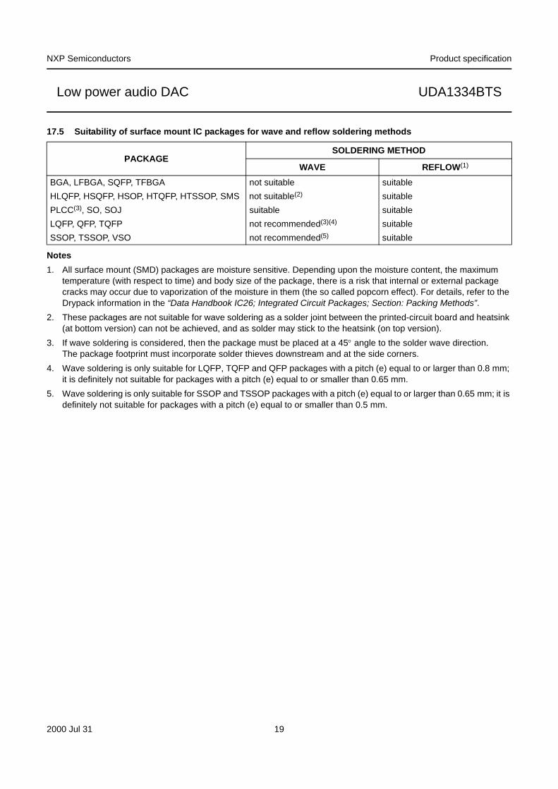
17.5 Suitability of surface mount IC packages for wave and reflow soldering methods
Notes1. All surface mount (SMD) packages are moisture sensitive. Depending upon the moisture content, the maximum
temperature (with respect to time) and body size of the package, there is a risk that internal or external package cracks may occur due to vaporization of the moisture in them (the so called popcorn effect). For details, refer to the Drypack information in the “Data Handbook IC26; Integrated Circuit Packages; Section: Packing Methods”.
2. These packages are not suitable for wave soldering as a solder joint between the printed-circuit board and heatsink (at bottom version) can not be achieved, and as solder may stick to the heatsink (on top version).
3. If wave soldering is considered, then the package must be placed at a 45° angle to the solder wave direction. The package footprint must incorporate solder thieves downstream and at the side corners.
4. Wave soldering is only suitable for LQFP, TQFP and QFP packages with a pitch (e) equal to or larger than 0.8 mm; it is definitely not suitable for packages with a pitch (e) equal to or smaller than 0.65 mm.
5. Wave soldering is only suitable for SSOP and TSSOP packages with a pitch (e) equal to or larger than 0.65 mm; it is definitely not suitable for packages with a pitch (e) equal to or smaller than 0.5 mm.
PACKAGESOLDERING METHOD
WAVE REFLOW(1)
BGA, LFBGA, SQFP, TFBGA not suitable suitableHLQFP, HSQFP, HSOP, HTQFP, HTSSOP, SMS not suitable(2) suitablePLCC(3), SO, SOJ suitable suitableLQFP, QFP, TQFP not recommended(3)(4) suitableSSOP, TSSOP, VSO not recommended(5) suitable
2000 Jul 31 19
NXP Semiconductors Product specification
Low power audio DAC UDA1334BTS
18 DATA SHEET STATUS
Notes1. Please consult the most recently issued document before initiating or completing a design.2. The product status of device(s) described in this document may have changed since this document was published
and may differ in case of multiple devices. The latest product status information is available on the Internet at URL http://www.nxp.com.
DOCUMENTSTATUS(1)
PRODUCT STATUS(2) DEFINITION
Objective data sheet Development This document contains data from the objective specification for product development.
Preliminary data sheet Qualification This document contains data from the preliminary specification. Product data sheet Production This document contains the product specification.
19 DISCLAIMERS
Limited warranty and liability ⎯ Information in this document is believed to be accurate and reliable. However, NXP Semiconductors does not give any representations or warranties, expressed or implied, as to the accuracy or completeness of such information and shall have no liability for the consequences of use of such information.
In no event shall NXP Semiconductors be liable for any indirect, incidental, punitive, special or consequential damages (including - without limitation - lost profits, lost savings, business interruption, costs related to the removal or replacement of any products or rework charges) whether or not such damages are based on tort (including negligence), warranty, breach of contract or any other legal theory.
Notwithstanding any damages that customer might incur for any reason whatsoever, NXP Semiconductors’ aggregate and cumulative liability towards customer for the products described herein shall be limited in accordance with the Terms and conditions of commercial sale of NXP Semiconductors.
Right to make changes ⎯ NXP Semiconductors reserves the right to make changes to information published in this document, including without limitation specifications and product descriptions, at any time and without notice. This document supersedes and replaces all information supplied prior to the publication hereof.
Suitability for use ⎯ NXP Semiconductors products are not designed, authorized or warranted to be suitable for use in life support, life-critical or safety-critical systems or equipment, nor in applications where failure or malfunction of an NXP Semiconductors product can reasonably be expected to result in personal injury, death or severe
property or environmental damage. NXP Semiconductors accepts no liability for inclusion and/or use of NXP Semiconductors products in such equipment or applications and therefore such inclusion and/or use is at the customer’s own risk.
Applications ⎯ Applications that are described herein for any of these products are for illustrative purposes only. NXP Semiconductors makes no representation or warranty that such applications will be suitable for the specified use without further testing or modification.
Customers are responsible for the design and operation of their applications and products using NXP Semiconductors products, and NXP Semiconductors accepts no liability for any assistance with applications or customer product design. It is customer’s sole responsibility to determine whether the NXP Semiconductors product is suitable and fit for the customer’s applications and products planned, as well as for the planned application and use of customer’s third party customer(s). Customers should provide appropriate design and operating safeguards to minimize the risks associated with their applications and products.
NXP Semiconductors does not accept any liability related to any default, damage, costs or problem which is based on any weakness or default in the customer’s applications or products, or the application or use by customer’s third party customer(s). Customer is responsible for doing all necessary testing for the customer’s applications and products using NXP Semiconductors products in order to avoid a default of the applications and the products or of the application or use by customer’s third party customer(s). NXP does not accept any liability in this respect.
2000 Jul 31 20
NXP Semiconductors Product specification
Low power audio DAC UDA1334BTS
Limiting values ⎯ Stress above one or more limiting values (as defined in the Absolute Maximum Ratings System of IEC 60134) will cause permanent damage to the device. Limiting values are stress ratings only and (proper) operation of the device at these or any other conditions above those given in the Recommended operating conditions section (if present) or the Characteristics sections of this document is not warranted. Constant or repeated exposure to limiting values will permanently and irreversibly affect the quality and reliability of the device.
Terms and conditions of commercial sale ⎯ NXP Semiconductors products are sold subject to the general terms and conditions of commercial sale, as published at http://www.nxp.com/profile/terms, unless otherwise agreed in a valid written individual agreement. In case an individual agreement is concluded only the terms and conditions of the respective agreement shall apply. NXP Semiconductors hereby expressly objects to applying the customer’s general terms and conditions with regard to the purchase of NXP Semiconductors products by customer.
No offer to sell or license ⎯ Nothing in this document may be interpreted or construed as an offer to sell products that is open for acceptance or the grant, conveyance or implication of any license under any copyrights, patents or other industrial or intellectual property rights.
Export control ⎯ This document as well as the item(s) described herein may be subject to export control regulations. Export might require a prior authorization from national authorities.
Quick reference data ⎯ The Quick reference data is an extract of the product data given in the Limiting values and Characteristics sections of this document, and as such is not complete, exhaustive or legally binding.
Non-automotive qualified products ⎯ Unless this data sheet expressly states that this specific NXP Semiconductors product is automotive qualified, the product is not suitable for automotive use. It is neither qualified nor tested in accordance with automotive testing or application requirements. NXP Semiconductors accepts no liability for inclusion and/or use of non-automotive qualified products in automotive equipment or applications.
In the event that customer uses the product for design-in and use in automotive applications to automotive specifications and standards, customer (a) shall use the product without NXP Semiconductors’ warranty of the product for such automotive applications, use and specifications, and (b) whenever customer uses the product for automotive applications beyond NXP Semiconductors’ specifications such use shall be solely at customer’s own risk, and (c) customer fully indemnifies NXP Semiconductors for any liability, damages or failed product claims resulting from customer design and use of the product for automotive applications beyond NXP Semiconductors’ standard warranty and NXP Semiconductors’ product specifications.
2000 Jul 31 21

NXP Semiconductors
provides High Performance Mixed Signal and Standard Product solutions that leverage its leading RF, Analog, Power Management, Interface, Security and Digital Processing expertise
Contact information
For additional information please visit: http://www.nxp.comFor sales offices addresses send e-mail to: [email protected]
© NXP B.V. 2010
All rights are reserved. Reproduction in whole or in part is prohibited without the prior written consent of the copyright owner.The information presented in this document does not form part of any quotation or contract, is believed to be accurate and reliable and may be changed without notice. No liability will be accepted by the publisher for any consequence of its use. Publication thereof does not convey nor imply any license
Customer notification
This data sheet was changed to reflect the new company name NXP Semiconductors, including new legal definitions and disclaimers. No changes were made to the technical content, except for package outline drawings which were updated to the latest version.
under patent- or other industrial or intellectual property rights.Printed in The Netherlands 753503/25/02/pp22 Date of release: 2000 Jul 31 Document order number: 9397 750 07239