Embed Size (px)
Citation preview
TLV320DAC3101
www.ti.com SLAS666A –JANUARY 2010–REVISED MAY 2012
Low-Power Stereo Audio DAC With Audio Processingand Stereo Class-D Speaker Amplifier
Check for Samples: TLV320DAC3101
1 INTRODUCTIONPlayback Volume-Control Settings1.1 Features
• Programmable PLL for Flexible Clock123• Stereo Audio DAC With 95-dB SNR Generation• Supports 8-kHz to 192-kHz Sample Rates • I2S, Left-Justified, Right-Justified, DSP, and• Stereo 1.29-W Class-D BTL 8-Ω Speaker Driver TDM Audio Interfaces
With Direct Battery Connection • I2C Control With Register Auto-Increment• 25 Built-In Processing Blocks (PRB_P1 – • Full Power-Down Control
PRB_P25) Providing Biquad Filters, DRC, and • Power Supplies:3D
– Analog: 2.7 V–3.6 V• Digital Sine-Wave Generator for Beeps and
– Digital Core: 1.65 V–1.95 VKey-Clicks (PRB_P25)– Digital I/O: 1.1 V–3.6 V• User-Programmable Biquad and FIR Filters– Class-D: 2.7 V–5.5 V (SPLVDD and SPRVDD• Two Single-Ended Inputs With Mixing and ≥ AVDD)Output Level Control
• 5-mm × 5-mm 32-QFN Package• Stereo Headphone/Lineout and Class-DSpeaker Outputs Available
1.2 Applications• Microphone Bias• Headphone Detection • Portable Audio Devices• Digital Mixing Capability • Mobile Internet Devices• Pin Control or Register Control for Digital- • e-Books
1.3 Description
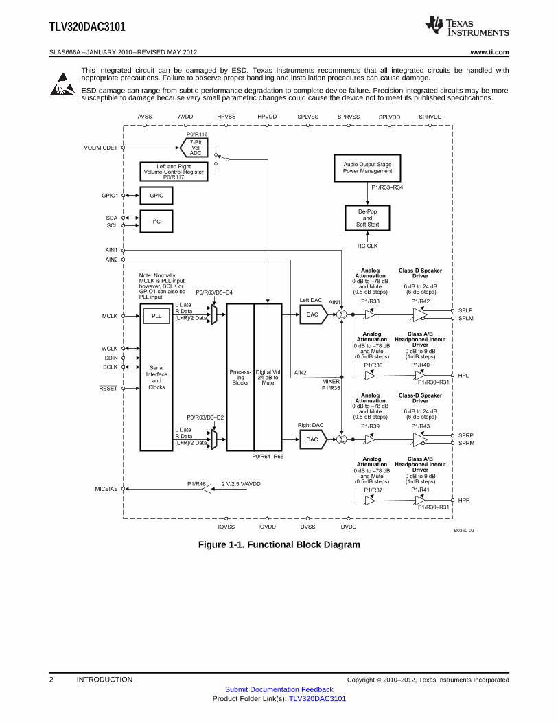
The TLV320DAC3101 is a low-power, highly integrated, high-performance DAC with selectable digitalaudio processing blocks and 24-bit stereo playback.
The device integrates headphone drivers and speaker drivers. The TLV320DAC3101 has a suite of built-inprocessing blocks for digital audio processing. The digital audio data format is programmable to work withpopular audio standard protocols (I2S, left/right-justified) in master, slave, DSP, and TDM modes. Bassboost, treble, or EQ can be supported by the programmable digital signal-processing block. An on-chipPLL provides the high-speed clock needed by the digital signal-processing block. The volume level can becontrolled by either pin control or by register control. The audio functions are controlled using the I2C serialbus.
The TLV320DAC3101 has a programmable digital sine-wave generator and is available in a 32-pin QFNpackage.
1
Please be aware that an important notice concerning availability, standard warranty, and use in critical applications ofTexas Instruments semiconductor products and disclaimers thereto appears at the end of this data sheet.
2MATLAB is a trademark of The MathWorks, Inc.3All other trademarks are the property of their respective owners.
PRODUCTION DATA information is current as of publication date. Products conform to Copyright © 2010–2012, Texas Instruments Incorporatedspecifications per the terms of the Texas Instruments standard warranty. Productionprocessing does not necessarily include testing of all parameters.
Serial
Interface
and
Clocks
SDIN
BCLK
WCLK
MCLK PLL
HPVDDHPVSS SPRVDDSPRVSSAVDDAVSS SPLVSS SPLVDD
VOL/MICDET
SCL
SDA
GPIOGPIO1
DAC
DAC
MIXER
P1/R35RESET
DVDDDVSSIOVDDIOVSS
AIN2
AIN2
AIN1
AIN1
2 V/2.5 V/AVDDMICBIAS
Note: Normally,MCLK is PLL input;however, BCLK orGPIO1 can also bePLL input.
Audio Output Stage
Power Management
De-Pop
and
Soft Start
RC CLK
P1/R33–R34
P1/R46
I C2
Left DAC
Right DAC
SPLP
SPLM
Class-D SpeakerDriver
6 dB to 24 dB(6-dB steps)
AnalogAttenuation
0 dB to –78 dBand Mute
(0.5-dB steps)
P1/R42P1/R38
Class A/BHeadphone/Lineout
Driver
0 dB to 9 dB(1-dB steps)
AnalogAttenuation
HPL
P1/R36 P1/R40
P1/R30–R31
L Data
L Data
R Data
R Data
(L+R)/2 Data
(L+R)/2 Data
P0/R63/D3–D2
P0/R63/D5–D4
P0/R116
7-BitVol
ADC
Left and RightVolume-Control Register
P0/R117
Digital Vol24 dB to
Mute
Process-ing
Blocks
P0/R64–R66
S
0 dB to –78 dBand Mute
(0.5-dB steps)
SPRP
SPRM
Class-D SpeakerDriver
6 dB to 24 dB(6-dB steps)
AnalogAttenuation
0 dB to –78 dBand Mute
(0.5-dB steps)
P1/R43P1/R39
Class A/BHeadphone/Lineout
Driver
0 dB to 9 dB(1-dB steps)
AnalogAttenuation
HPR
P1/R37 P1/R41
P1/R30–R31
S
0 dB to –78 dBand Mute
(0.5-dB steps)
B0360-02
TLV320DAC3101
SLAS666A –JANUARY 2010–REVISED MAY 2012 www.ti.com
This integrated circuit can be damaged by ESD. Texas Instruments recommends that all integrated circuits be handled withappropriate precautions. Failure to observe proper handling and installation procedures can cause damage.
ESD damage can range from subtle performance degradation to complete device failure. Precision integrated circuits may be moresusceptible to damage because very small parametric changes could cause the device not to meet its published specifications.
Figure 1-1. Functional Block Diagram
2 INTRODUCTION Copyright © 2010–2012, Texas Instruments Incorporated
Submit Documentation FeedbackProduct Folder Link(s): TLV320DAC3101
TLV320DAC3101
www.ti.com SLAS666A –JANUARY 2010–REVISED MAY 2012
NOTEThis data manual is designed using PDF document-viewing features that allow quick accessto information. For example, performing a global search on "page 0 / register 27" producesall references to this page and register in a list. This makes it easy to traverse the list andfind all information related to a page and register. Note that the search string must be of theindicated format. Also, this document includes document hyperlinks to allow the user toquickly find a document reference. To come back to the original page, click the green leftarrow near the PDF page number at the bottom of the file. The hot-key for this function is alt-left arrow on the keyboard. Another way to find information quickly is to use the PDFbookmarks.
Copyright © 2010–2012, Texas Instruments Incorporated INTRODUCTION 3Submit Documentation Feedback
Product Folder Link(s): TLV320DAC3101
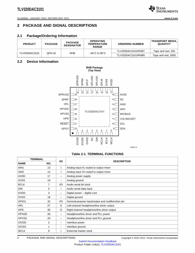
P0048-14
AVSSSPRVSS
IOV
SS
SP
RV
DD
24
1
23
2
22
3
21
4
20
5
19
6
18
7
17
8
1625
1526
1427
1328
1229
1130
1031
932
NC
SP
RM
AIN2
SP
LP
AIN1
SP
LV
DD
MICBIAS
SP
LV
SS
VOL/MICDET
SP
LM
SCL
DV
SS
SDA
AV
DD
RHB Package(Top View)
SPRP
IOV
DD
HPL
DV
DD
HPVDD
NC
HPVSS
DIN
HPR
WC
LK
RESET
BC
LK
GPIO1
MC
LK
TLV320DAC3101
TLV320DAC3101
SLAS666A –JANUARY 2010–REVISED MAY 2012 www.ti.com
2 PACKAGE AND SIGNAL DESCRIPTIONS
2.1 Package/Ordering InformationOPERATING TRANSPORT MEDIA,PACKAGEPRODUCT PACKAGE TEMPERATURE ORDERING NUMBER QUANTITYDESIGNATOR RANGE
TLV320DAC3101IRHBT Tape and reel, 250TLV320DAC3101 QFN-32 RHB –40°C to 85°C
TLV320DAC3101IRHBR Tape and reel, 3000
2.2 Device Information
Table 2-1. TERMINAL FUNCTIONS
TERMINALI/O DESCRIPTION
NAME NO.
AIN1 13 I Analog input #1 routed to output mixer
AIN2 14 I Analog input #2 routed to output mixer
AVDD 17 – Analog power supply
AVSS 16 – Analog ground
BCLK 7 I/O Audio serial bit clock
DIN 5 I Audio serial data input
DVDD 3 – Digital power – digital core
DVSS 18 – Digital ground
GPIO1 32 I/O General-purpose input/output and multifunction pin
HPL 27 O Left-channel headphone/line driver output
HPR 30 O Right-channel headphone/line driver output
HPVDD 28 – Headphone/line driver and PLL power
HPVSS 29 – Headphone/line driver and PLL ground
IOVDD 2 – Interface power
IOVSS 1 – Interface ground
MCLK 8 I Exterrnal master clock
4 PACKAGE AND SIGNAL DESCRIPTIONS Copyright © 2010–2012, Texas Instruments Incorporated
Submit Documentation FeedbackProduct Folder Link(s): TLV320DAC3101
TLV320DAC3101
www.ti.com SLAS666A –JANUARY 2010–REVISED MAY 2012
Table 2-1. TERMINAL FUNCTIONS (continued)
TERMINALI/O DESCRIPTION
NAME NO.
MICBIAS 12 – Microphone bias for external microphone
NC 4,15 I No connecton
RESET 31 I Device reset
SCL 10 I/O I2C control bus clock input
SDA 9 I/O I2C control bus data input
SPLM 19 O Left-channel class-D speaker-driver inverting output
SPLP 22 O Left-channel class-D speaker-driver noninverting output
SPLVDD 21 – Left-channel class-D speaker-driver power supply
SPLVSS 20 – Left-channel class-D speaker-driver power supply ground
SPRM 23 O Right-channel class-D speaker-driver inverting output
SPRP 26 O Right-channel class-D speaker-driver noninverting output
SPRVDD 24 – Right-channel class-D speaker-driver power supply
SPRVSS 25 – Right-channel class-D speaker-driver power-supply ground
Volume control or headphone detection. Note that microphone detection is also available onVOL/MICDET 11 I devices that have an ADC.
WCLK 6 I/O Audio serial word clock
3 ELECTRICAL SPECIFICATIONS
3.1 Absolute Maximum Ratingsover operating free-air temperature range (unless otherwise noted) (1)
VALUE UNIT
AVDD to AVSS –0.3 to 3.9 V
DVDD to DVSS –0.3 to 2.5 V
HPVDD to HPVSS –0.3 to 3.9 V
SPLVDD to SPLVSS –0.3 to 6 V
SPRVDD to SPRVSS –0.3 to 6 V
IOVDD to IOVSS –0.3 to 3.9 V
Digital input voltage IOVSS – 0.3 to IOVDD + 0.3 V
Analog input voltage AVSS – 0.3 to AVDD + 0.3 V
Operating temperature range –40 to 85 °C
Storage temperature range –55 to 150 °C
Junction temperature (TJ Max) 105 °C
Power dissipation (TJ Max – TA)/RθJA W
RθJA thermal impedance (with thermal pad soldered to board) 35 °C/W
(1) Stresses beyond those listed under Absolute Maximum Ratings may cause permanent damage to the device. These are stress ratingsonly, and functional operation of the device at these or any other conditions beyond those indicated under Recommended OperatingConditions is not implied. Exposure to absolute-maximum-rated conditions for extended periods may affect device reliability.
Table 3-1. System Thermal Characteristics (1)
Power Rating at 25°C Derating Factor Power Rating at 70°C Power Rating at 85°C
2.3 W 28.57 mW/°C 1 W 0.6 W
(1) This data was taken using 2-oz. (0.071-mm thick) trace and copper pad that is soldered to a JEDEC high-K, standard 4-layer 3-in. × 3-in. (7.62-cm × 7.62-cm) PCB.
Copyright © 2010–2012, Texas Instruments Incorporated ELECTRICAL SPECIFICATIONS 5Submit Documentation Feedback
Product Folder Link(s): TLV320DAC3101
TLV320DAC3101
SLAS666A –JANUARY 2010–REVISED MAY 2012 www.ti.com
3.2 Recommended Operating Conditionsover operating free-air temperature range (unless otherwise noted)
MIN NOM MAX UNIT
AVDD (1) Referenced to AVSS (2) 2.7 3.3 3.6
DVDD Referenced to DVSS(2) 1.65 1.8 1.95
HPVDD Referenced to HPVSS(2) 2.7 3.3 3.6 VPower-supply voltage range
SPLVDD (1) Referenced to SPLVSS(2) 2.7 5.5
SPRVDD (1) Referenced to SPRVSS(2) 2.7 5.5
IOVDD Referenced to IOVSS(2) 1.1 3.3 3.6
Resistance applied across class-D output pinsSpeaker impedance 8 Ω(BTL)
Headphone impedance AC-coupled to RL 16 ΩAnalog audio full-scale inputVI AVDD = 3.3 V, single-ended 0.707 VRMSvoltage
Stereo line output load AC coupled to RL 10 kΩimpedance
MCLK (3) Master clock frequency IOVDD = 3.3 V 50 MHz
fSCL SCL clock frequency 400 kHz
TA Operating free-air temperature –40 85 °C
(1) To minimize battery-current leakage, the SPLVDD and SPRVDD voltage levels should not be below the AVDD voltage level.(2) All grounds on board are tied together, so they should not differ in voltage by more than 0.2 V maximum for any combination of ground
signals. By use of a wide trace or ground plane, ensure a low-impedance connection between HPVSS and DVSS.(3) The maximum input frequency should be 50 MHz for any digital pin used as a general-purpose clock.
3.3 Electrical CharacteristicsAt 25°C, AVDD = HPVDD = IOVDD = 3.3 V, SPLVDD, SPRVDD = 3.6 V, DVDD = 1.8 V, fS (audio) = 48 kHz, CODEC_CLKIN= 256 × fS, PLL = Off, VOL/MICDET pin disabled (unless otherwise noted)
PARAMETER TEST CONDITIONS MIN TYP MAX UNIT
INTERNAL OSCILLATOR—RC_CLK
Oscillator frequency 8.2 MHz
VOLUME CONTROL PIN (ADC); VOL/MICDET PIN ENABLED
VOL/MICDET pin configured as volume control 0.5 ×Input voltage range (page 0 / register 116, bit D7 = 1 and page 0 / 0 VAVDDregister 67, bit D7 = 0)
Input capacitance 2 pF
Volume control steps 128 Steps
MICROPHONE BIAS
Page 1 / register 46, bits D1–D0 = 10 2.25 2.5 2.75Voltage output V
Page 1 / register 46, bits D1–D0 = 01 2
At 4-mA load current, page 1 / register 46, bits D1–D0 5= 10 (MICBIAS = 2.5 V)Voltage regulation mV
At 4-mA load current, page 1 / register 46, bits D1–D0 7= 01 (MICBIAS = 2 V)
6 ELECTRICAL SPECIFICATIONS Copyright © 2010–2012, Texas Instruments Incorporated
Submit Documentation FeedbackProduct Folder Link(s): TLV320DAC3101
TLV320DAC3101
www.ti.com SLAS666A –JANUARY 2010–REVISED MAY 2012
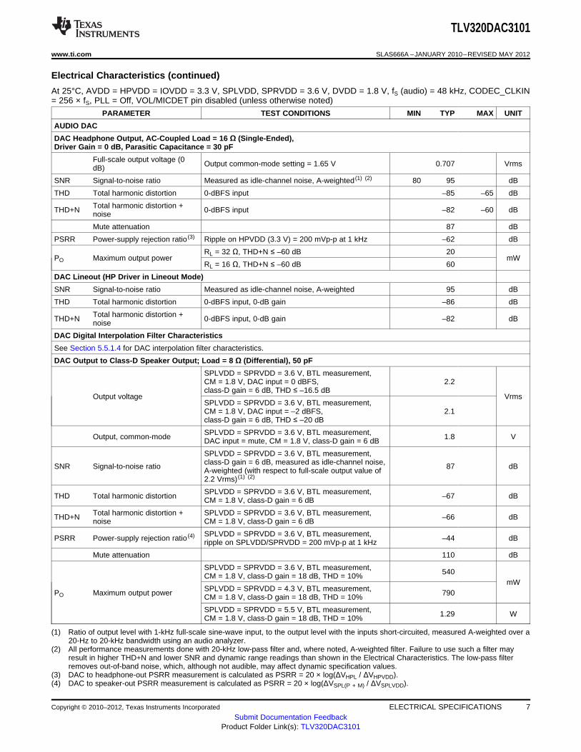
Electrical Characteristics (continued)
At 25°C, AVDD = HPVDD = IOVDD = 3.3 V, SPLVDD, SPRVDD = 3.6 V, DVDD = 1.8 V, fS (audio) = 48 kHz, CODEC_CLKIN= 256 × fS, PLL = Off, VOL/MICDET pin disabled (unless otherwise noted)
PARAMETER TEST CONDITIONS MIN TYP MAX UNIT
AUDIO DAC
DAC Headphone Output, AC-Coupled Load = 16 Ω (Single-Ended),Driver Gain = 0 dB, Parasitic Capacitance = 30 pF
Full-scale output voltage (0 Output common-mode setting = 1.65 V 0.707 VrmsdB)
SNR Signal-to-noise ratio Measured as idle-channel noise, A-weighted (1) (2) 80 95 dB
THD Total harmonic distortion 0-dBFS input –85 –65 dB
Total harmonic distortion +THD+N 0-dBFS input –82 –60 dBnoise
Mute attenuation 87 dB
PSRR Power-supply rejection ratio (3) Ripple on HPVDD (3.3 V) = 200 mVp-p at 1 kHz –62 dB
RL = 32 Ω, THD+N ≤ –60 dB 20PO Maximum output power mW
RL = 16 Ω, THD+N ≤ –60 dB 60
DAC Lineout (HP Driver in Lineout Mode)
SNR Signal-to-noise ratio Measured as idle-channel noise, A-weighted 95 dB
THD Total harmonic distortion 0-dBFS input, 0-dB gain –86 dB
Total harmonic distortion +THD+N 0-dBFS input, 0-dB gain –82 dBnoise
DAC Digital Interpolation Filter Characteristics
See Section 5.5.1.4 for DAC interpolation filter characteristics.
DAC Output to Class-D Speaker Output; Load = 8 Ω (Differential), 50 pF
SPLVDD = SPRVDD = 3.6 V, BTL measurement,CM = 1.8 V, DAC input = 0 dBFS, 2.2class-D gain = 6 dB, THD ≤ –16.5 dB
Output voltage VrmsSPLVDD = SPRVDD = 3.6 V, BTL measurement,CM = 1.8 V, DAC input = –2 dBFS, 2.1class-D gain = 6 dB, THD ≤ –20 dB
SPLVDD = SPRVDD = 3.6 V, BTL measurement,Output, common-mode 1.8 VDAC input = mute, CM = 1.8 V, class-D gain = 6 dB
SPLVDD = SPRVDD = 3.6 V, BTL measurement,class-D gain = 6 dB, measured as idle-channel noise,SNR Signal-to-noise ratio 87 dBA-weighted (with respect to full-scale output value of2.2 Vrms) (1) (2)
SPLVDD = SPRVDD = 3.6 V, BTL measurement,THD Total harmonic distortion –67 dBCM = 1.8 V, class-D gain = 6 dB
Total harmonic distortion + SPLVDD = SPRVDD = 3.6 V, BTL measurement,THD+N –66 dBnoise CM = 1.8 V, class-D gain = 6 dB
SPLVDD = SPRVDD = 3.6 V, BTL measurement,PSRR Power-supply rejection ratio (4) –44 dBripple on SPLVDD/SPRVDD = 200 mVp-p at 1 kHz
Mute attenuation 110 dB
SPLVDD = SPRVDD = 3.6 V, BTL measurement, 540CM = 1.8 V, class-D gain = 18 dB, THD = 10%mW
SPLVDD = SPRVDD = 4.3 V, BTL measurement,PO Maximum output power 790CM = 1.8 V, class-D gain = 18 dB, THD = 10%
SPLVDD = SPRVDD = 5.5 V, BTL measurement, 1.29 WCM = 1.8 V, class-D gain = 18 dB, THD = 10%
(1) Ratio of output level with 1-kHz full-scale sine-wave input, to the output level with the inputs short-circuited, measured A-weighted over a20-Hz to 20-kHz bandwidth using an audio analyzer.
(2) All performance measurements done with 20-kHz low-pass filter and, where noted, A-weighted filter. Failure to use such a filter mayresult in higher THD+N and lower SNR and dynamic range readings than shown in the Electrical Characteristics. The low-pass filterremoves out-of-band noise, which, although not audible, may affect dynamic specification values.
(3) DAC to headphone-out PSRR measurement is calculated as PSRR = 20 × log(ΔVHPL / ΔVHPVDD).(4) DAC to speaker-out PSRR measurement is calculated as PSRR = 20 × log(ΔVSPL(P + M) / ΔVSPLVDD).
Copyright © 2010–2012, Texas Instruments Incorporated ELECTRICAL SPECIFICATIONS 7Submit Documentation Feedback
Product Folder Link(s): TLV320DAC3101
TLV320DAC3101
SLAS666A –JANUARY 2010–REVISED MAY 2012 www.ti.com
Electrical Characteristics (continued)
At 25°C, AVDD = HPVDD = IOVDD = 3.3 V, SPLVDD, SPRVDD = 3.6 V, DVDD = 1.8 V, fS (audio) = 48 kHz, CODEC_CLKIN= 256 × fS, PLL = Off, VOL/MICDET pin disabled (unless otherwise noted)
PARAMETER TEST CONDITIONS MIN TYP MAX UNIT
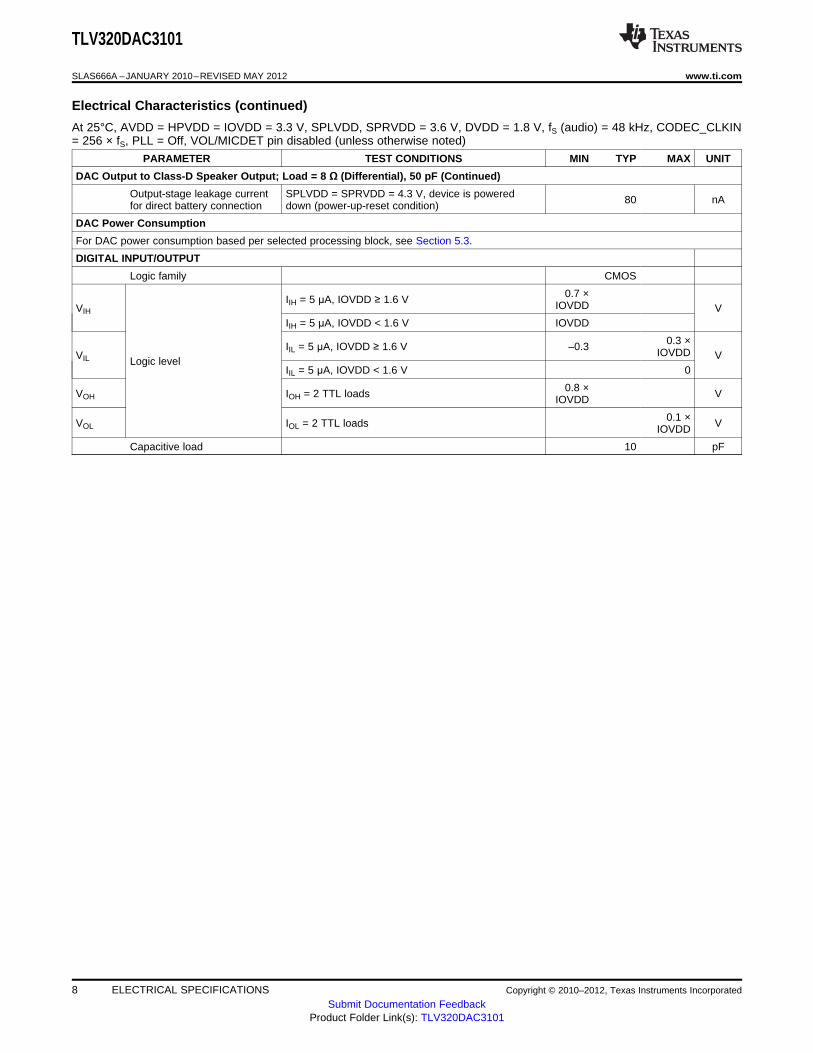
DAC Output to Class-D Speaker Output; Load = 8 Ω (Differential), 50 pF (Continued)
Output-stage leakage current SPLVDD = SPRVDD = 4.3 V, device is powered 80 nAfor direct battery connection down (power-up-reset condition)
DAC Power Consumption
For DAC power consumption based per selected processing block, see Section 5.3.
DIGITAL INPUT/OUTPUT
Logic family CMOS
0.7 ×IIH = 5 μA, IOVDD ≥ 1.6 V IOVDDVIH VIIH = 5 μA, IOVDD < 1.6 V IOVDD
0.3 ×IIL = 5 μA, IOVDD ≥ 1.6 V –0.3 IOVDDVIL VLogic levelIIL = 5 μA, IOVDD < 1.6 V 0
0.8 ×VOH IOH = 2 TTL loads VIOVDD
0.1 ×VOL IOL = 2 TTL loads VIOVDD
Capacitive load 10 pF
8 ELECTRICAL SPECIFICATIONS Copyright © 2010–2012, Texas Instruments Incorporated
Submit Documentation FeedbackProduct Folder Link(s): TLV320DAC3101
T0145-10
WCLK
BCLK
DIN
t (WS)d
t (DI)S t (DI)h
tr
tf
TLV320DAC3101
www.ti.com SLAS666A –JANUARY 2010–REVISED MAY 2012
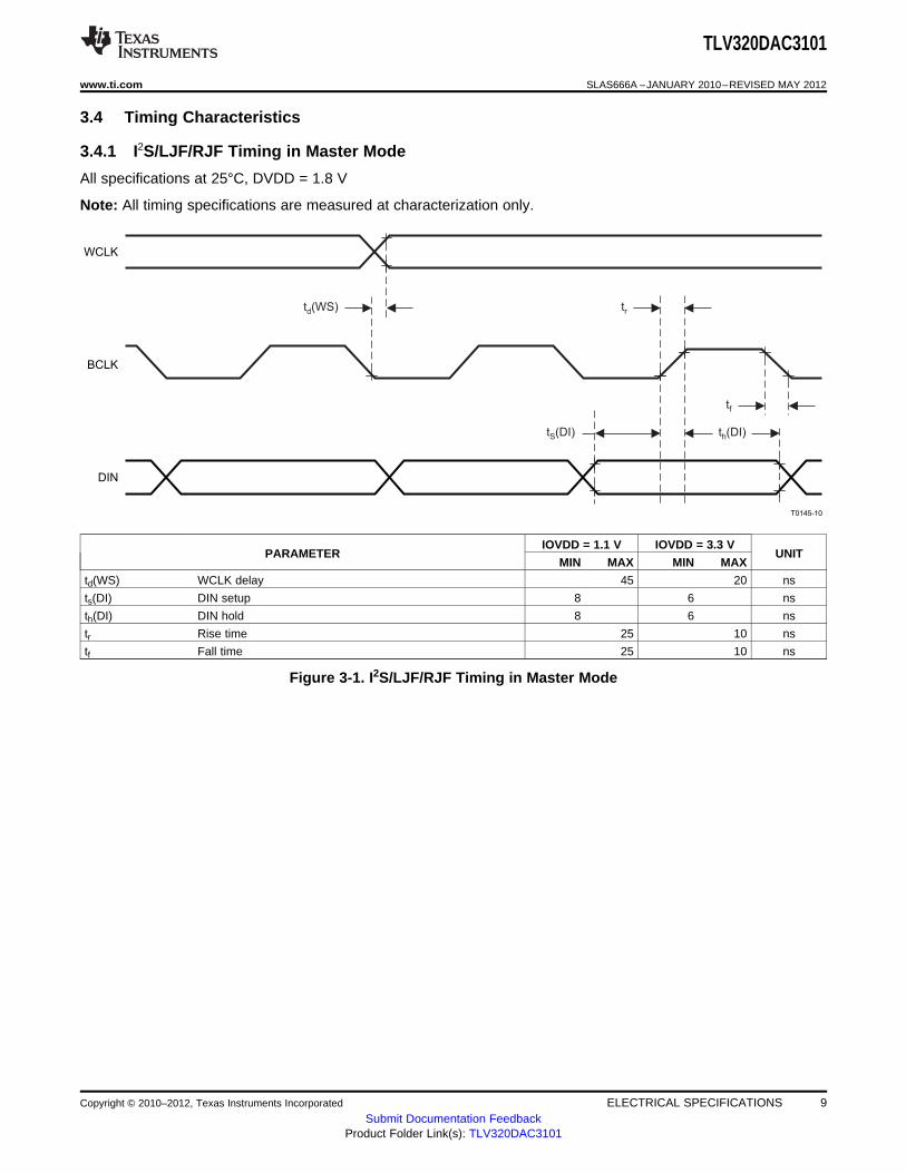
3.4 Timing Characteristics
3.4.1 I2S/LJF/RJF Timing in Master Mode
All specifications at 25°C, DVDD = 1.8 V
Note: All timing specifications are measured at characterization only.
IOVDD = 1.1 V IOVDD = 3.3 VPARAMETER UNIT
MIN MAX MIN MAX
td(WS) WCLK delay 45 20 ns
ts(DI) DIN setup 8 6 ns
th(DI) DIN hold 8 6 ns
tr Rise time 25 10 ns
tf Fall time 25 10 ns
Figure 3-1. I2S/LJF/RJF Timing in Master Mode
Copyright © 2010–2012, Texas Instruments Incorporated ELECTRICAL SPECIFICATIONS 9Submit Documentation Feedback
Product Folder Link(s): TLV320DAC3101
T0145-11
WCLK
BCLK
DIN
t (WS)h
t (BCLK)H
t (DI)S
t (BCLK)L
t (DI)h
t (WS)S
tr
tf
TLV320DAC3101
SLAS666A –JANUARY 2010–REVISED MAY 2012 www.ti.com
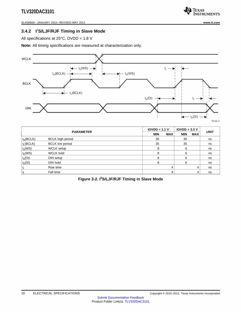
3.4.2 I2S/LJF/RJF Timing in Slave Mode
All specifications at 25°C, DVDD = 1.8 V
Note: All timing specifications are measured at characterization only.
IOVDD = 1.1 V IOVDD = 3.3 VPARAMETER UNIT
MIN MAX MIN MAX
tH(BCLK) BCLK high period 35 35 ns
tL(BCLK) BCLK low period 35 35 ns
ts(WS) WCLK setup 8 6 ns
th(WS) WCLK hold 8 6 ns
ts(DI) DIN setup 8 6 ns
th(DI) DIN hold 8 6 ns
tr Rise time 4 4 ns
tf Fall time 4 4 ns
Figure 3-2. I2S/LJF/RJF Timing in Slave Mode
10 ELECTRICAL SPECIFICATIONS Copyright © 2010–2012, Texas Instruments Incorporated
Submit Documentation FeedbackProduct Folder Link(s): TLV320DAC3101
T0146-09
WCLK
BCLK
DIN
t (WS)d t (WS)d
t (DI)S
t (DI)h
tf
tr
TLV320DAC3101
www.ti.com SLAS666A –JANUARY 2010–REVISED MAY 2012
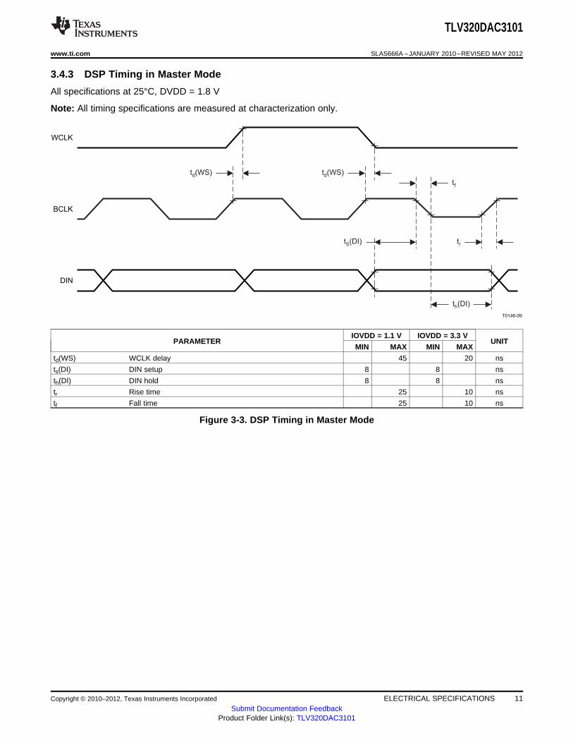
3.4.3 DSP Timing in Master Mode
All specifications at 25°C, DVDD = 1.8 V
Note: All timing specifications are measured at characterization only.
IOVDD = 1.1 V IOVDD = 3.3 VPARAMETER UNIT
MIN MAX MIN MAX
td(WS) WCLK delay 45 20 ns
ts(DI) DIN setup 8 8 ns
th(DI) DIN hold 8 8 ns
tr Rise time 25 10 ns
tf Fall time 25 10 ns
Figure 3-3. DSP Timing in Master Mode
Copyright © 2010–2012, Texas Instruments Incorporated ELECTRICAL SPECIFICATIONS 11Submit Documentation Feedback
Product Folder Link(s): TLV320DAC3101
T0146-10
WCLK
BCLK
DIN
t (WS)h t (WS)h
t (BCLK)L
tr
tf
t (DI)St (BCLK)H
t (DI)h
t (WS)S t (WS)S
TLV320DAC3101
SLAS666A –JANUARY 2010–REVISED MAY 2012 www.ti.com
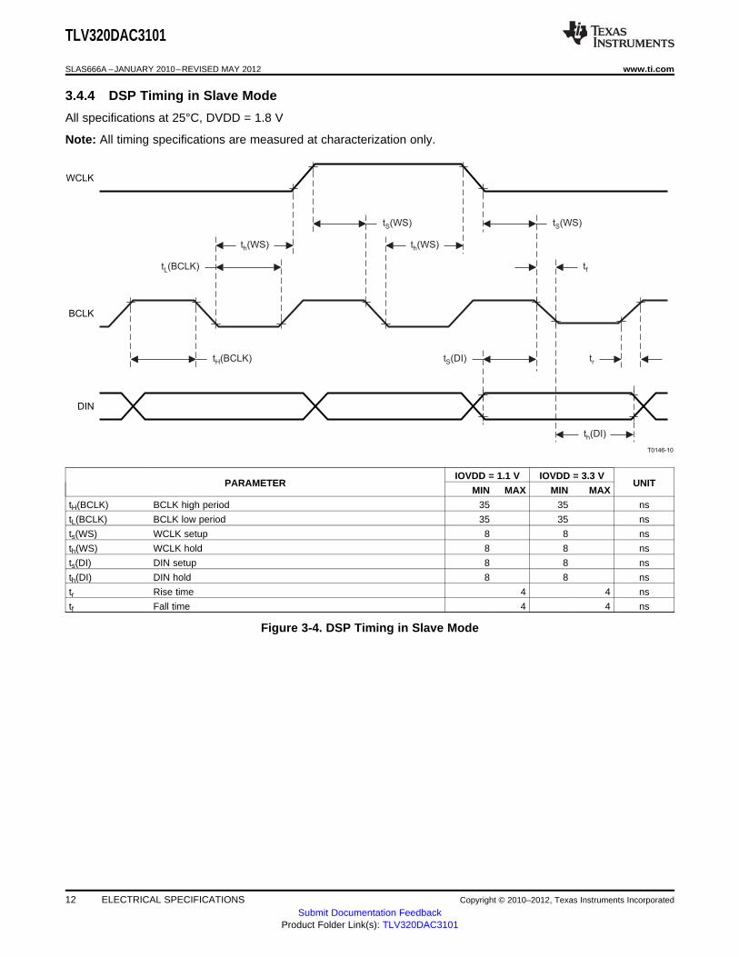
3.4.4 DSP Timing in Slave Mode
All specifications at 25°C, DVDD = 1.8 V
Note: All timing specifications are measured at characterization only.
IOVDD = 1.1 V IOVDD = 3.3 VPARAMETER UNIT
MIN MAX MIN MAX
tH(BCLK) BCLK high period 35 35 ns
tL(BCLK) BCLK low period 35 35 ns
ts(WS) WCLK setup 8 8 ns
th(WS) WCLK hold 8 8 ns
ts(DI) DIN setup 8 8 ns
th(DI) DIN hold 8 8 ns
tr Rise time 4 4 ns
tf Fall time 4 4 ns
Figure 3-4. DSP Timing in Slave Mode
12 ELECTRICAL SPECIFICATIONS Copyright © 2010–2012, Texas Instruments Incorporated
Submit Documentation FeedbackProduct Folder Link(s): TLV320DAC3101
STO STA STA STO
SDA
SCL
tBUF tLOW
tSU;STA
tHIGH tHD;STA
tr
tHD;STA
tHD;DAT
tSU;DAT tSU;STO
tf
T0295-02
TLV320DAC3101
www.ti.com SLAS666A –JANUARY 2010–REVISED MAY 2012
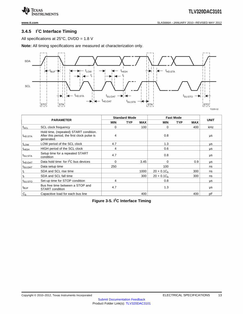
3.4.5 I2C Interface Timing
All specifications at 25°C, DVDD = 1.8 V
Note: All timing specifications are measured at characterization only.
Standard Mode Fast ModePARAMETER UNIT
MIN TYP MAX MIN TYP MAX
fSCL SCL clock frequency 0 100 0 400 kHz
Hold time, (repeated) START condition.tHD;STA After this period, the first clock pulse is 4 0.8 μs
generated.
tLOW LOW period of the SCL clock 4.7 1.3 μs
tHIGH HIGH period of the SCL clock 4 0.6 μs
Setup time for a repeated STARTtSU;STA 4.7 0.8 μscondition
tHD;DAT Data hold time: for I2C bus devices 0 3.45 0 0.9 μs
tSU;DAT Data setup time 250 100 ns
tr SDA and SCL rise time 1000 20 + 0.1Cb 300 ns
tf SDA and SCL fall time 300 20 + 0.1Cb 300 ns
tSU;STO Set-up time for STOP condition 4 0.8 μs
Bus free time between a STOP andtBUF 4.7 1.3 μsSTART condition
Cb Capacitive load for each bus line 400 400 pF
Figure 3-5. I2C Interface Timing
Copyright © 2010–2012, Texas Instruments Incorporated ELECTRICAL SPECIFICATIONS 13Submit Documentation Feedback
Product Folder Link(s): TLV320DAC3101
f − Frequency − kHz
−160
−140
−120
−100
−80
−60
−40
−20
0
20
0 5 10 15 20
Am
plitu
de −
dB
FS
G023
AVDD = HPVDD = 3.3 VIOVDD = SPLVDD = 3.3 VDVDD = 1.8 V
f − Frequency − kHz
−160
−140
−120
−100
−80
−60
−40
−20
0
20
0 5 10 15 20
Am
plitu
de −
dB
FS
G026
AVDD = HPVDD = 3.3 VIOVDD = SPLVDD = 3.3 VDVDD = 1.8 V
−100
−90
−80
−70
−60
−50
−40
−30
−20
−10
0
0.00 0.02 0.04 0.06 0.08 0.10 0.12 0.14
G025
TH
D+N
− T
otal
Har
mon
ic D
isto
rtio
n +
Noi
se −
dB
PO − Output Power − W
HPVDD = 3.3 VCM = 1.65 V
HPVDD = 3.6 VCM = 1.8 V
HPVDD = 3 VCM = 1.5 V
HPVDD = 2.7 VCM = 1.35 V
IOVDD = 3.3 VDVDD = 1.8 VGain = 9 dBRL = 16 Ω
TLV320DAC3101
SLAS666A –JANUARY 2010–REVISED MAY 2012 www.ti.com
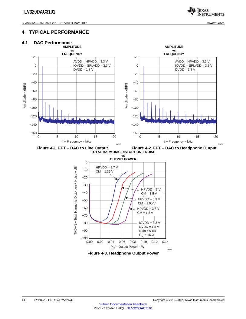
4 TYPICAL PERFORMANCE
4.1 DAC PerformanceAMPLITUDE AMPLITUDE
vs vsFREQUENCY FREQUENCY
Figure 4-1. FFT – DAC to Line Output Figure 4-2. FFT – DAC to Headphone OutputTOTAL HARMONIC DISTORTION + NOISE
vsOUTPUT POWER
Figure 4-3. Headphone Output Power
14 TYPICAL PERFORMANCE Copyright © 2010–2012, Texas Instruments Incorporated
Submit Documentation FeedbackProduct Folder Link(s): TLV320DAC3101
−80
−70
−60
−50
−40
−30
−20
−10
0
0.0 0.5 1.0 1.5 2.0
G014
TH
D+N
− T
otal
Har
mon
ic D
isto
rtio
n +
Noi
se −
dB
PO − Output Power − W
Driver Gain= 6 dB
Driver Gain= 12 dB
AVDD = HPVDD = 3.3 VIOVDD = 3.3 VSPLVDD = 5.5 VDVDD = 1.8 VRL = 8 Ω
Driver Gain= 24 dB
Driver Gain= 18 dB
−80
−70
−60
−50
−40
−30
−20
−10
0
0.0 0.5 1.0 1.5 2.0
G015
TH
D+N
− T
otal
Har
mon
ic D
isto
rtio
n +
Noi
se −
dB
PO − Output Power − W
AVDD = 3.3 VHPVDD = 3.3 VIOVDD = 3.3 VDVDD = 1.8 VGain = 18 dBRL = 8 ΩSPLVDD = 5.5 V
SPLVDD = 4.3 V
SPLVDD = 3.3 V
SPLVDD = 3.6 V
f − Frequency − kHz
−160
−140
−120
−100
−80
−60
−40
−20
0
20
0 5 10 15 20
Am
plitu
de −
dB
FS
G024
AVDD = HPVDD = 3.3 VIOVDD = SPLVDD = 3.3 VDVDD = 1.8 V
f − Frequency − kHz
−160
−140
−120
−100
−80
−60
−40
−20
0
20
0 5 10 15 20
Am
plitu
de −
dB
FS
G027
AVDD = HPVDD = 3.3 VIOVDD = SPLVDD = 3.3 VDVDD = 1.8 V
TLV320DAC3101
www.ti.com SLAS666A –JANUARY 2010–REVISED MAY 2012
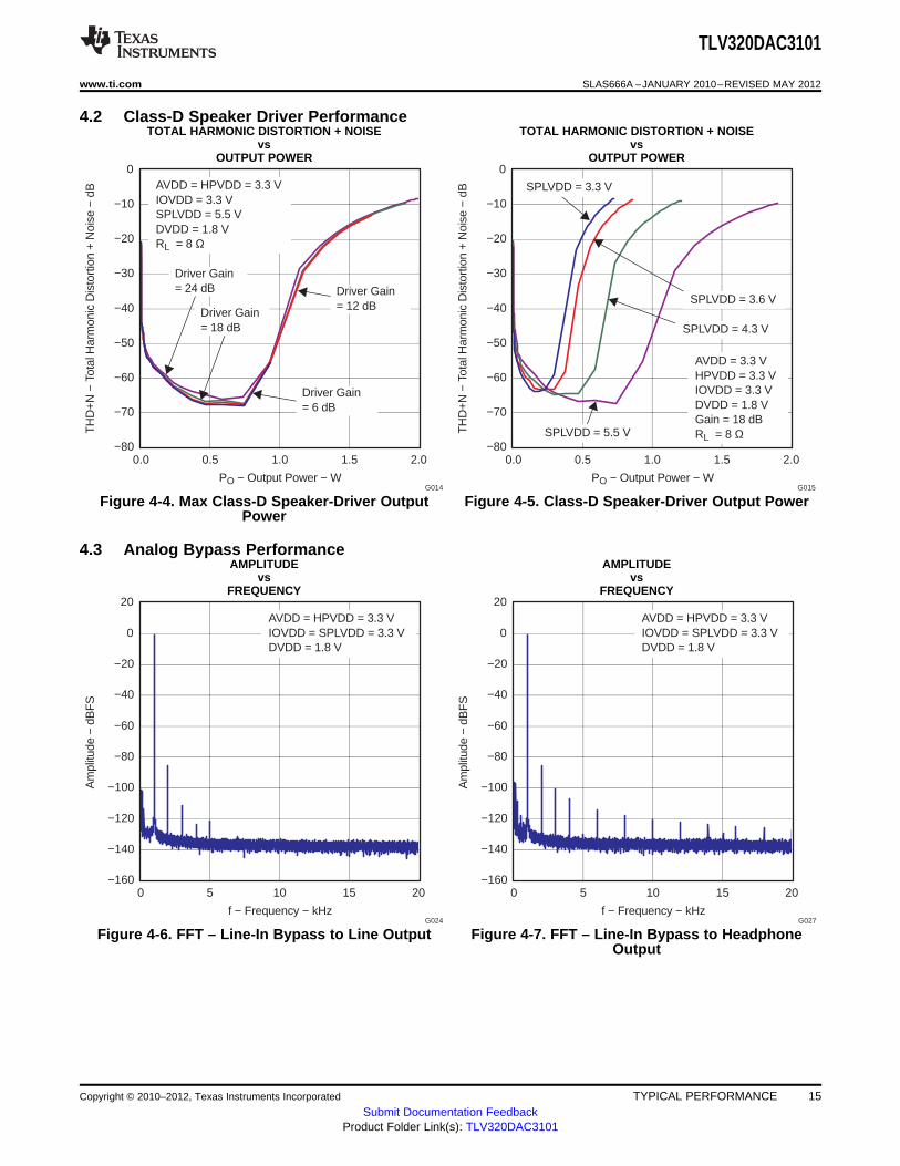
4.2 Class-D Speaker Driver PerformanceTOTAL HARMONIC DISTORTION + NOISE TOTAL HARMONIC DISTORTION + NOISE
vs vsOUTPUT POWER OUTPUT POWER
Figure 4-4. Max Class-D Speaker-Driver Output Figure 4-5. Class-D Speaker-Driver Output PowerPower
4.3 Analog Bypass PerformanceAMPLITUDE AMPLITUDE
vs vsFREQUENCY FREQUENCY
Figure 4-6. FFT – Line-In Bypass to Line Output Figure 4-7. FFT – Line-In Bypass to HeadphoneOutput
Copyright © 2010–2012, Texas Instruments Incorporated TYPICAL PERFORMANCE 15Submit Documentation Feedback
Product Folder Link(s): TLV320DAC3101
I − Current − mA
0.0
0.5
1.0
1.5
2.0
2.5
3.0
3.5
0.0 0.5 1.0 1.5 2.0 2.5 3.0 3.5 4.0
V −
Vol
tage
− V
G016
Micbias = 2 V
Micbias = 2.5 V
Micbias = AVDD (3.3 V)
TLV320DAC3101
SLAS666A –JANUARY 2010–REVISED MAY 2012 www.ti.com
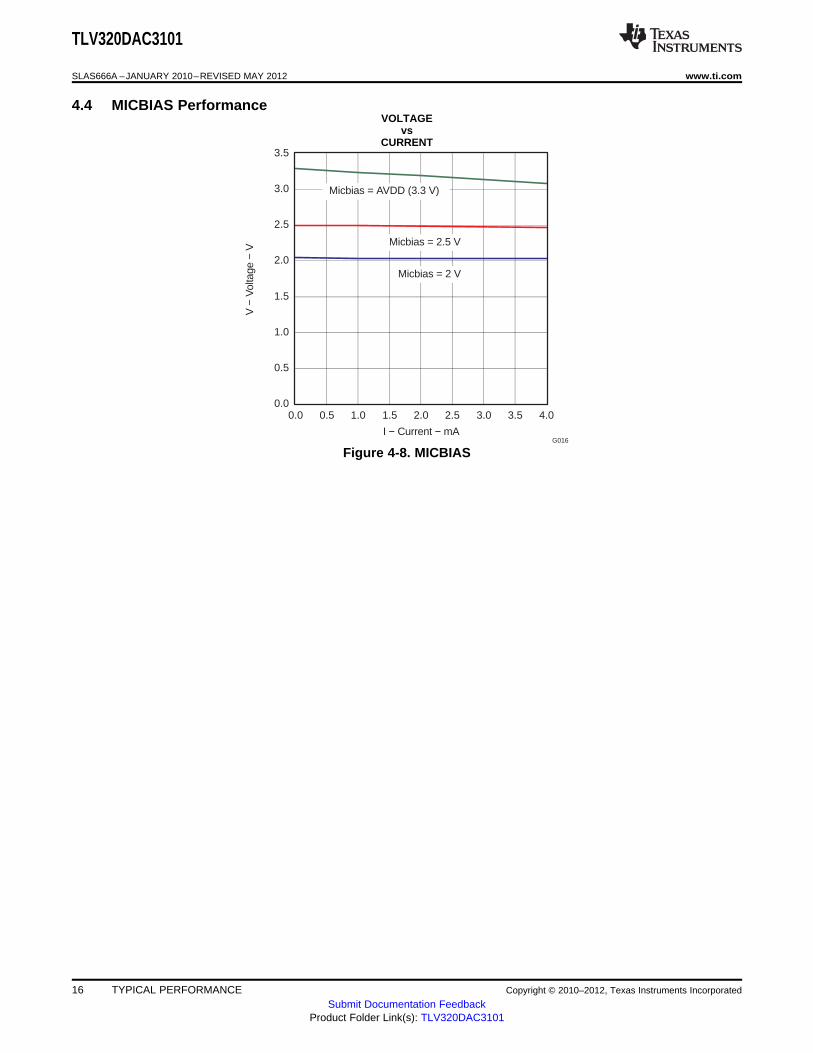
4.4 MICBIAS PerformanceVOLTAGE
vsCURRENT
Figure 4-8. MICBIAS
16 TYPICAL PERFORMANCE Copyright © 2010–2012, Texas Instruments Incorporated
Submit Documentation FeedbackProduct Folder Link(s): TLV320DAC3101
HPVDD HPVSSSPKVDD SPKVSS AVDD AVSSSPKVSS
VOL/MICDET
MICBIAS
TLV320DAC3101
SPKVDD
22 Fm0.1 Fm0.1 Fm 22 Fm
SVDD
AVDD
AVSS
0.1 Fm 10 Fm0.1 Fm 10 Fm
+3.3VA
1 Fm
DVDD DVSS IOVDD IOVSS
0.1 Fm 10 Fm
+1.8VD IOVDD
0.1 Fm 10 Fm
HO
ST
PR
OC
ES
SO
R
SDIN
BCLK
WCLK
MCLK
SCL
SDA
RESET
GPIO1
S0400-05
AIN1
AIN2
To ExternalMIC Circuitry
Analog In
SPRPSPRM
SPLPSPLM
HPR
HPL
8-Speaker
W
8-Speaker
W
StereoHeadphoneOut
34.8 kW
25 kW
9.76 kW
TLV320DAC3101
www.ti.com SLAS666A –JANUARY 2010–REVISED MAY 2012
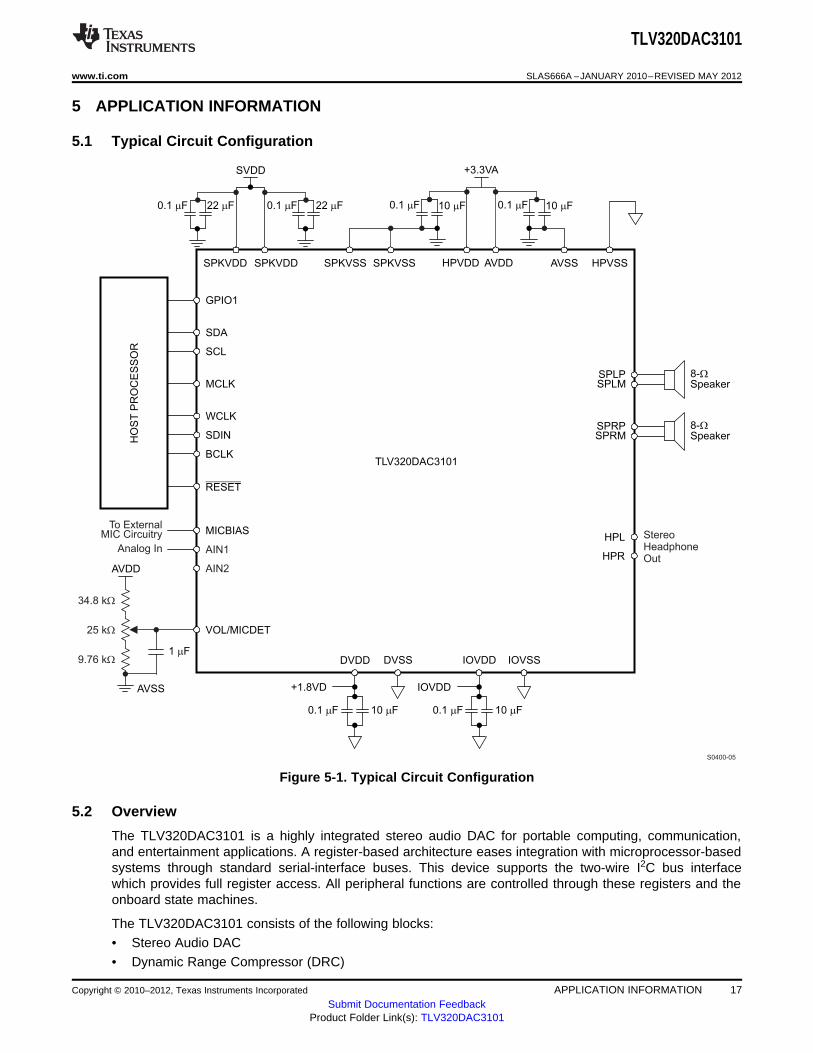
5 APPLICATION INFORMATION
5.1 Typical Circuit Configuration
Figure 5-1. Typical Circuit Configuration
5.2 Overview
The TLV320DAC3101 is a highly integrated stereo audio DAC for portable computing, communication,and entertainment applications. A register-based architecture eases integration with microprocessor-basedsystems through standard serial-interface buses. This device supports the two-wire I2C bus interfacewhich provides full register access. All peripheral functions are controlled through these registers and theonboard state machines.
The TLV320DAC3101 consists of the following blocks:• Stereo Audio DAC• Dynamic Range Compressor (DRC)
Copyright © 2010–2012, Texas Instruments Incorporated APPLICATION INFORMATION 17Submit Documentation Feedback
Product Folder Link(s): TLV320DAC3101
TLV320DAC3101
SLAS666A –JANUARY 2010–REVISED MAY 2012 www.ti.com
• Digital sine-wave generator for clicks and beeps• Stereo headphone/lineout amplifier• Class-D stereo amplifier for 8-Ω speakers• Pin-controlled or register-controlled volume level• Power-down de-pop and power-up soft start• Analog inputs• I2C control interface• Power-down control block
Following a toggle of the RESET pin or a software reset, the device operates in the default mode. The I2Cinterface is used to write to the control registers to configure the device.
The I2C address assigned to the TLV320DAC3101 is 001 1000. This device always operates in an I2Cslave mode. All registers are 8-bit, and all writable registers have read-back capability. The device auto-increments to support sequential addressing and can be used with I2C fast mode. Once the device isreset, all appropriate registers are updated by the host processor to configure the device as needed by theuser.
5.2.1 Device Initialization
5.2.1.1 Reset
The TLV320DAC3101 internal logic must be initialized to a known condition for proper device function. Toinitialize the device to its default operating condition, the hardware reset pin (RESET) must be pulled lowfor at least 10 ns. For this initialization to work, both the IOVDD and DVDD supplies must be powered up.It is recommended that while the DVDD supply is being powered up, the RESET pin be pulled low.
The device can also be reset via software reset. Writing a 1 into page 0 / register 1, bit D0 resets thedevice.
5.2.1.2 Device Start-Up Lockout Times
After the TLV320DAC3101 is initialized by hardware reset at power up or by software reset, the internalmemories are initialized to default values. This initialization takes place within 1 ms after pulling theRESET signal high. During this initialization phase, no register-read or register-write operation should beperformed on DAC coefficient buffers. Also, no block within the codec should be powered up during theinitialization phase.
5.2.1.3 PLL Start-Up
Whenever the PLL is powered up, a start-up delay of approximately of 10 ms occurs after the power-upcommand of the PLL and before the clocks are available to the codec. This delay is to ensure stableoperation of the PLL and clock-divider logic.
5.2.1.4 Power-Stage Reset
The power-stage-only reset is used to reset the device after an overcurrent latching shutdown hasoccurred. Using this reset re-enables the output stage without resetting all of the registers in the device.Each of the four power stages has its own dedicated reset bit. The headphone power-stage reset isperformed by setting page 1 / register 31, bit D7 for HPL and by setting page 1 / register 31, bit D6 forHPR. The speaker power-stage reset is performed by setting page 1 / register 32, bit D7 for SPLP andSPLM, and by setting page 1 / register 32, bit D6 for SPRP and SPRM.
18 APPLICATION INFORMATION Copyright © 2010–2012, Texas Instruments Incorporated
Submit Documentation FeedbackProduct Folder Link(s): TLV320DAC3101
TLV320DAC3101
www.ti.com SLAS666A –JANUARY 2010–REVISED MAY 2012
5.2.1.5 Software Power Down
By default, all circuit blocks are powered down following a reset condition. Hardware power up of eachcircuit block can be controlled by writing to the appropriate control register. This approach allows thelowest power-supply current for the functionality required. However, when a block is powered down, all ofthe register settings are maintained as long as power is still being applied to the device.
5.2.2 Audio Analog I/O
The TLV320DAC3101 has a stereo audio DAC. It has a wide range of analog interfaces to supportdifferent headsets and analog outputs. The TLV320DAC3101 has features to interface with output drivers(8-Ω, 16-Ω, 32-Ω). A special circuit has also been included in the TLV320DAC3101 to insert a short key-click sound into the stereo audio output. The key-click sound is used to provide feedback to the user whena particular button is pressed or item is selected. The specific sound of the keyclick can be adjusted byvarying several register bits that control its frequency, duration, and amplitude. See Key-Click FunctionalityWith Digital Sine-Wave Generator (PRB_P25), Section 5.5.7.
5.3 Digital Processing Low-Power Modes
The TLV320DAC3101 device can be tuned to minimize power dissipation, to maximize performance, or toan operating point between the two extremes to best fit the application. The choice of processing blocks,PRB_P1 to PRB_P25 for stereo playback, also influences the power consumption. In fact, the numerousprocessing blocks have been implemented to offer a choice among configurations having a differentbalance of power optimization and signal-processing capabilities.
Copyright © 2010–2012, Texas Instruments Incorporated APPLICATION INFORMATION 19Submit Documentation Feedback
Product Folder Link(s): TLV320DAC3101
TLV320DAC3101
SLAS666A –JANUARY 2010–REVISED MAY 2012 www.ti.com
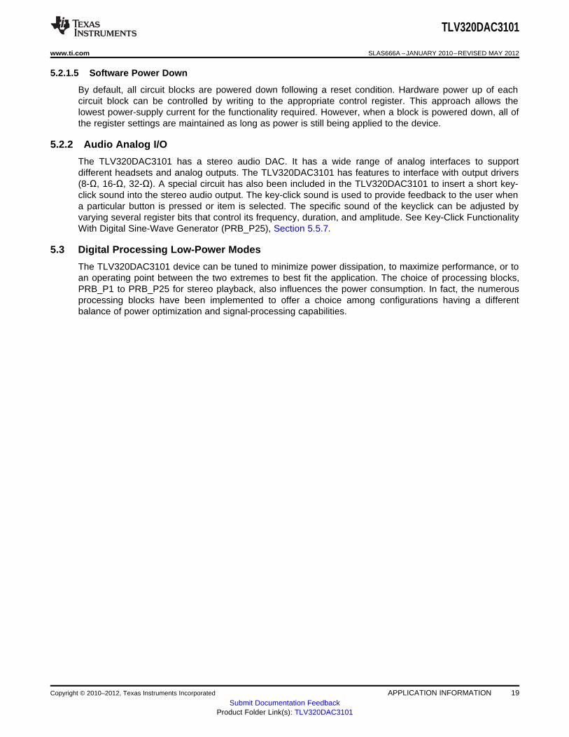
5.3.1 DAC Playback on Headphones, Stereo, 48 kHz, DVDD = 1.8 V, AVDD = 3.3 V,HPVDD = 3.3 V
DOSR = 128, Processing Block = PRB_P7 (Interpolation Filter B)
Power consumption = 24.28 mW
Table 5-1. PRB_P7 Alternative Processing Blocks, 24.28 mW
Processing Block Filter Estimated Power Change (mW)
PRB_P1 A 1.34
PRB_P2 A 2.86
PRB_P3 A 2.11
PRB_P8 B 1.18
PRB_P9 B 0.53
PRB_P10 B 1.89
PRB_P11 B 0.87
PRB_P23 A 1.48
PRB_P24 A 2.89
PRB_P25 A 3.23
DOSR = 64, Processing Block = PRB_P7 (Interpolation Filter B)
Power consumption = 24.5 mW
Table 5-2. PRB_P7 Alternative Processing Blocks, 24.5 mW
Processing Block Filter Estimated Power Change (mW)
PRB_P1 A 1.17
PRB_P2 A 2.62
PRB_P3 A 2
PRB_P8 B 0.99
PRB_P9 B 0.5
PRB_P10 B 1.46
PRB_P11 B 0.66
PRB_P23 A 1.43
PRB_P24 A 2.69
PRB_P25 A 2.92
5.3.2 DAC Playback on Headphones, Mono, 48 kHz, DVDD = 1.8 V, AVDD = 3.3 V,HPVDD = 3.3 V
DOSR = 128, Processing Block = PRB_P12 (Interpolation Filter B)
Power consumption = 15.4 mW
Table 5-3. PRB_P12 Alternative Processing Blocks, 15.4 mW
Processing Block Filter Estimated Power Change (mW)
PRB_P4 A 0.57
PRB_P5 A 1.48
PRB_P6 A 1.08
PRB_P13 B 0.56
PRB_P14 B 0.27
PRB_P15 B 0.89
PRB_P16 B 0.31
20 APPLICATION INFORMATION Copyright © 2010–2012, Texas Instruments Incorporated
Submit Documentation FeedbackProduct Folder Link(s): TLV320DAC3101
TLV320DAC3101
www.ti.com SLAS666A –JANUARY 2010–REVISED MAY 2012
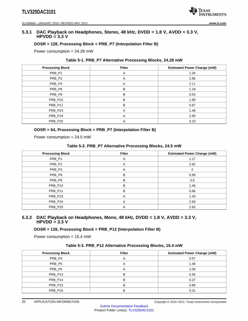
DOSR = 64, Processing Block = PRB_P12 (Interpolation Filter B)
Power consumption = 15.54 mW
Table 5-4. PRB_P12 Alternative Processing Blocks, 15.54 mW
Processing Block Filter Estimated Power Change (mW)
PRB_P4 A 0.37
PRB_P5 A 1.23
PRB_P6 A 1.15
PRB_P13 B 0.43
PRB_P14 B 0.13
PRB_P15 B 0.85
PRB_P16 B 0.21
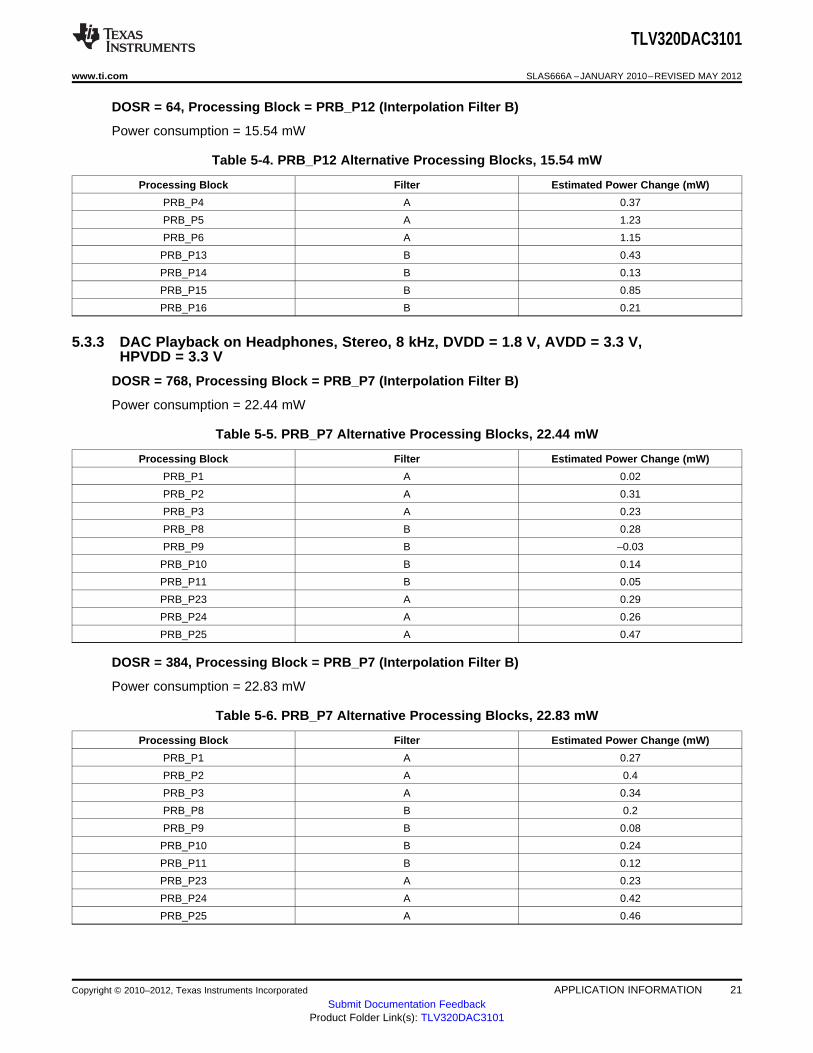
5.3.3 DAC Playback on Headphones, Stereo, 8 kHz, DVDD = 1.8 V, AVDD = 3.3 V,HPVDD = 3.3 V
DOSR = 768, Processing Block = PRB_P7 (Interpolation Filter B)
Power consumption = 22.44 mW
Table 5-5. PRB_P7 Alternative Processing Blocks, 22.44 mW
Processing Block Filter Estimated Power Change (mW)
PRB_P1 A 0.02
PRB_P2 A 0.31
PRB_P3 A 0.23
PRB_P8 B 0.28
PRB_P9 B –0.03
PRB_P10 B 0.14
PRB_P11 B 0.05
PRB_P23 A 0.29
PRB_P24 A 0.26
PRB_P25 A 0.47
DOSR = 384, Processing Block = PRB_P7 (Interpolation Filter B)
Power consumption = 22.83 mW
Table 5-6. PRB_P7 Alternative Processing Blocks, 22.83 mW
Processing Block Filter Estimated Power Change (mW)
PRB_P1 A 0.27
PRB_P2 A 0.4
PRB_P3 A 0.34
PRB_P8 B 0.2
PRB_P9 B 0.08
PRB_P10 B 0.24
PRB_P11 B 0.12
PRB_P23 A 0.23
PRB_P24 A 0.42
PRB_P25 A 0.46
Copyright © 2010–2012, Texas Instruments Incorporated APPLICATION INFORMATION 21Submit Documentation Feedback
Product Folder Link(s): TLV320DAC3101
TLV320DAC3101
SLAS666A –JANUARY 2010–REVISED MAY 2012 www.ti.com
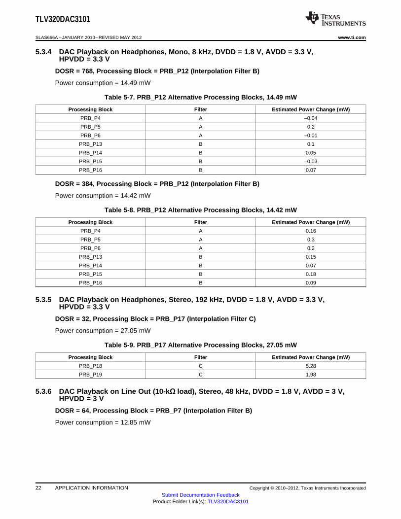
5.3.4 DAC Playback on Headphones, Mono, 8 kHz, DVDD = 1.8 V, AVDD = 3.3 V,HPVDD = 3.3 V
DOSR = 768, Processing Block = PRB_P12 (Interpolation Filter B)
Power consumption = 14.49 mW
Table 5-7. PRB_P12 Alternative Processing Blocks, 14.49 mW
Processing Block Filter Estimated Power Change (mW)
PRB_P4 A –0.04
PRB_P5 A 0.2
PRB_P6 A –0.01
PRB_P13 B 0.1
PRB_P14 B 0.05
PRB_P15 B –0.03
PRB_P16 B 0.07
DOSR = 384, Processing Block = PRB_P12 (Interpolation Filter B)
Power consumption = 14.42 mW
Table 5-8. PRB_P12 Alternative Processing Blocks, 14.42 mW
Processing Block Filter Estimated Power Change (mW)
PRB_P4 A 0.16
PRB_P5 A 0.3
PRB_P6 A 0.2
PRB_P13 B 0.15
PRB_P14 B 0.07
PRB_P15 B 0.18
PRB_P16 B 0.09
5.3.5 DAC Playback on Headphones, Stereo, 192 kHz, DVDD = 1.8 V, AVDD = 3.3 V,HPVDD = 3.3 V
DOSR = 32, Processing Block = PRB_P17 (Interpolation Filter C)
Power consumption = 27.05 mW
Table 5-9. PRB_P17 Alternative Processing Blocks, 27.05 mW
Processing Block Filter Estimated Power Change (mW)
PRB_P18 C 5.28
PRB_P19 C 1.98
5.3.6 DAC Playback on Line Out (10-kΩ load), Stereo, 48 kHz, DVDD = 1.8 V, AVDD = 3 V,HPVDD = 3 V
DOSR = 64, Processing Block = PRB_P7 (Interpolation Filter B)
Power consumption = 12.85 mW
22 APPLICATION INFORMATION Copyright © 2010–2012, Texas Instruments Incorporated
Submit Documentation FeedbackProduct Folder Link(s): TLV320DAC3101
TLV320DAC3101
www.ti.com SLAS666A –JANUARY 2010–REVISED MAY 2012
5.4 Analog Signals
The TLV320DAC3101 analog signals consist of:• Microphone bias (MICBIAS)• Analog inputs AIN1 and AIN2• Analog outputs class-D speaker driver and headphone/lineout driver providing output capability for the
DAC, AIN1, AIN2 or a mix of the three
5.4.1 MICBIAS
The TLV320DAC3101 includes a microphone bias circuit which can source up to 4 mA of current and isprogrammable to a 2-V, 2.5-V, or AVDD level. The level can be controlled by writing to page 1 /register 46, bits D1–D0. This functionality is shown in Table 5-10.
Table 5-10. MICBIAS Settings
D1 D0 FUNCTIONALITY
0 0 MICBIAS output is powered down.
0 1 MICBIAS output is powered to 2 V.
1 0 MICBIAS output is powered to 2.5 V.
1 1 MICBIAS output is powered to AVDD.
During normal operation, MICBIAS can be set to 2.5 V for better performance. However, depending on themodel of microphone that is selected, optimal performance might be obtained at another setting, so theperformance at a given setting should be verified.
The lowest current consumption occurs when MICBIAS is powered down. The next-lowest currentconsumption occurs when MICBIAS is set at AVDD.
5.4.2 Analog Inputs AIN1 and AIN2
AIN1 (pin 13) and AIN2 (pin 14) are inputs to the output mixer along with the DAC output. Page 1 /register 35 provides control signals for determining the signals routed through the output mixer. The outputof the output mixer then can be attenuated or gained through the class-D and/or headphone/lineoutdrivers.
5.5 Audio DAC and Audio Analog Outputs
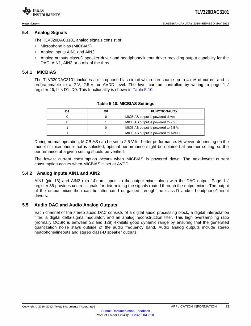
Each channel of the stereo audio DAC consists of a digital audio processing block, a digital interpolationfilter, a digital delta-sigma modulator, and an analog reconstruction filter. This high oversampling ratio(normally DOSR is between 32 and 128) exhibits good dynamic range by ensuring that the generatedquantization noise stays outside of the audio frequency band. Audio analog outputs include stereoheadphone/lineouts and stereo class-D speaker outputs.
Copyright © 2010–2012, Texas Instruments Incorporated APPLICATION INFORMATION 23Submit Documentation Feedback
Product Folder Link(s): TLV320DAC3101
TLV320DAC3101
SLAS666A –JANUARY 2010–REVISED MAY 2012 www.ti.com
5.5.1 DAC
The TLV320DAC3101 stereo audio DAC supports data rates from 8 kHz to 192 kHz. Each channel of thestereo audio DAC consists of a signal-processing engine with fixed processing blocks, a digitalinterpolation filter, multibit digital delta-sigma modulator, and an analog reconstruction filter. The DAC isdesigned to provide enhanced performance at low sampling rates through increased oversampling andimage filtering, thereby keeping quantization noise generated within the delta-sigma modulator and signalimages strongly suppressed within the audio band to beyond 20 kHz. To handle multiple input rates andoptimize power dissipation and performance, the TLV320DAC3101 allows the system designer to programthe oversampling rates over a wide range from 1 to 1024 by configuring page 0 / register 13 and page 0 /register 14. The system designer can choose higher oversampling ratios for lower input data rates andlower oversampling ratios for higher input data rates.
The TLV320DAC3101 DAC channel includes a built-in digital interpolation filter to generate oversampleddata for the delta-sigma modulator. The interpolation filter can be chosen from three different types,depending on required frequency response, group delay, and sampling rate.
DAC power up is controlled by writing to page 0 / register 63, bit D7 for the left channel and bit D6 for theright channel. The left-channel DAC clipping flag is provided as a read-only bit on page 0 / register 39,bit D7. The right-channel DAC clipping flag is provided as a read-only bit on page 0 / register 39, bit D6.
5.5.1.1 DAC Processing Blocks
The TLV320DAC3101 implements signal-processing capabilities and interpolation filtering via processingblocks. These fixed processing blocks give users the choice of how much and what type of signalprocessing they use and which interpolation filter is applied.
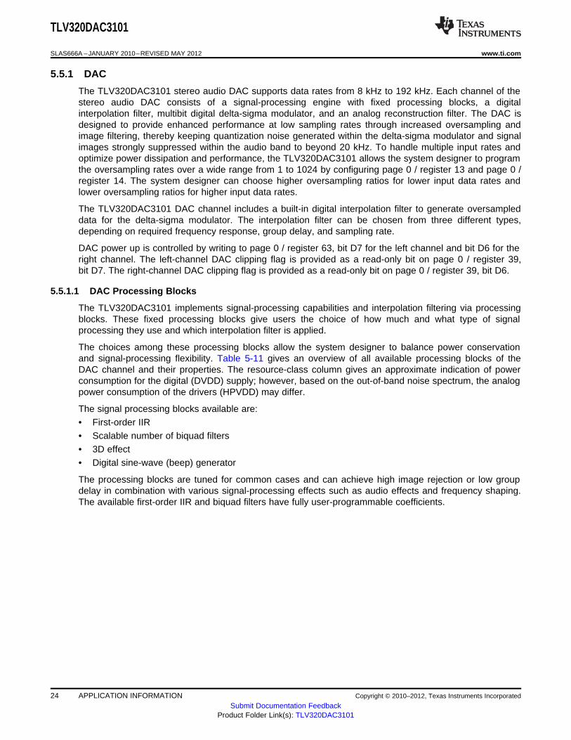
The choices among these processing blocks allow the system designer to balance power conservationand signal-processing flexibility. Table 5-11 gives an overview of all available processing blocks of theDAC channel and their properties. The resource-class column gives an approximate indication of powerconsumption for the digital (DVDD) supply; however, based on the out-of-band noise spectrum, the analogpower consumption of the drivers (HPVDD) may differ.
The signal processing blocks available are:• First-order IIR• Scalable number of biquad filters• 3D effect• Digital sine-wave (beep) generator
The processing blocks are tuned for common cases and can achieve high image rejection or low groupdelay in combination with various signal-processing effects such as audio effects and frequency shaping.The available first-order IIR and biquad filters have fully user-programmable coefficients.
24 APPLICATION INFORMATION Copyright © 2010–2012, Texas Instruments Incorporated
Submit Documentation FeedbackProduct Folder Link(s): TLV320DAC3101
Interp.
Filter A
BiQuad
C
BiQuad
B
BiQuad
Ato
Modulator
Digital
Volume
Ctrl
from
Interface
´
Interp.
Filter
A,B
DRCHPF
BiQuad
F
BiQuad
E
BiQuad
D
BiQuad
C
BiQuad
B
BiQuad
AIIR to
Modulator
Digital
Volume
Ctrl
from
Interface
´
TLV320DAC3101
www.ti.com SLAS666A –JANUARY 2010–REVISED MAY 2012
Table 5-11. Overview – DAC Predefined Processing Blocks
NumberProcessing Interpolation First-Order Beep ResourceChannel of DRC 3DBlock No. Filter IIR Available Generator ClassBiquads
PRB_P1 A Stereo No 3 No No No 8
PRB_P2 A Stereo Yes 6 Yes No No 12
PRB_P3 A Stereo Yes 6 No No No 10
PRB_P4 A Left No 3 No No No 4
PRB_P5 A Left Yes 6 Yes No No 6
PRB_P6 A Left Yes 6 No No No 6
PRB_P7 B Stereo Yes 0 No No No 6
PRB_P8 B Stereo No 4 Yes No No 8
PRB_P9 B Stereo No 4 No No No 8
PRB_P10 B Stereo Yes 6 Yes No No 10
PRB_P11 B Stereo Yes 6 No No No 8
PRB_P12 B Left Yes 0 No No No 3
PRB_P13 B Left No 4 Yes No No 4
PRB_P14 B Left No 4 No No No 4
PRB_P15 B Left Yes 6 Yes No No 6
PRB_P16 B Left Yes 6 No No No 4
PRB_P17 C Stereo Yes 0 No No No 3
PRB_P18 C Stereo Yes 4 Yes No No 6
PRB_P19 C Stereo Yes 4 No No No 4
PRB_P20 C Left Yes 0 No No No 2
PRB_P21 C Left Yes 4 Yes No No 3
PRB_P22 C Left Yes 4 No No No 2
PRB_P23 A Stereo No 2 No Yes No 8
PRB_P24 A Stereo Yes 5 Yes Yes No 12
PRB_P25 A Stereo Yes 5 Yes Yes Yes 12
5.5.1.2 DAC Processing Blocks – Signal Chain Details
5.5.1.2.1 Three Biquads, Filter A
Figure 5-2. Signal Chain for PRB_P1 and PRB_P4
5.5.1.2.2 Six Biquads, First-Order IIR, DRC, Filter A or B
Figure 5-3. Signal Chain for PRB_P2, PRB_P5, PRB_P10, and PRB_P15
Copyright © 2010–2012, Texas Instruments Incorporated APPLICATION INFORMATION 25Submit Documentation Feedback
Product Folder Link(s): TLV320DAC3101
Interp.
Filter
A,B
BiQuad
F
BiQuad
E
BiQuad
D
BiQuad
C
BiQuad
B
BiQuad
AIIR to
Modulator
Digital
Volume
Ctrl
from
Interface
´
Interp.
Filter
B,C
IIR to
Modulator
Digital
Volume
Ctrl
from
Interface
´
Interp.
Filter B
DRCHPF
to
Modulator
Digital
Volume
Ctrl
BiQuad
D
BiQuad
C
BiQuad
B
BiQuad
Afrom
Interface
´
Interp.
Filter B
BiQuad
D
BiQuad
C
BiQuad
B
BiQuad
Ato
Modulator
Digital
Volume
Ctrl
from
Interface
´
Interp.
Filter C
DRCHPF
IIR to
Modulator
Digital
Volume
Ctrl
BiQuad
D
BiQuad
C
BiQuad
B
BiQuad
A
from
Interface
´
TLV320DAC3101
SLAS666A –JANUARY 2010–REVISED MAY 2012 www.ti.com
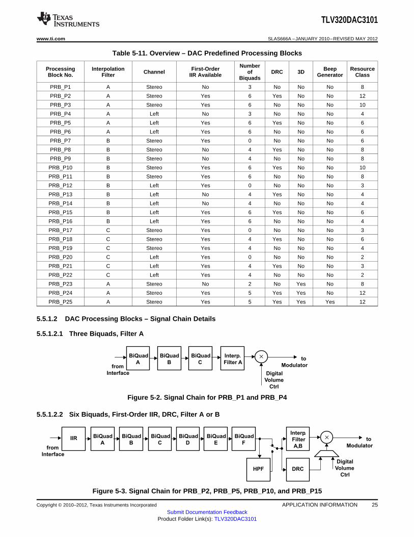
5.5.1.2.3 Six Biquads, First-Order IIR, Filter A or B
Figure 5-4. Signal Chain for PRB_P3, PRB_P6, PRB_P11, and PRB_P16
5.5.1.2.4 IIR, Filter B or C
Figure 5-5. Signal Chain for PRB_P7, PRB_P12, PRB_P17, and PRB_P20
5.5.1.2.5 Four Biquads, DRC, Filter B
Figure 5-6. Signal Chain for PRB_P8 and PRB_P13
5.5.1.2.6 Four Biquads, Filter B
Figure 5-7. Signal Chain for PRB_P9 and PRB_P14
5.5.1.2.7 Four Biquads, First-Order IIR, DRC, Filter C
Figure 5-8. Signal Chain for PRB_P18 and PRB_P21
26 APPLICATION INFORMATION Copyright © 2010–2012, Texas Instruments Incorporated
Submit Documentation FeedbackProduct Folder Link(s): TLV320DAC3101
Interp.
Filter C
BiQuad
D
BiQuad
C
BiQuad
B
BiQuad
AIIR to
modulator
Digital
Volume
Ctrl
from
Interface
´
3DPGA
+
+
+
+
–
+
–
+
+
FromLeft-
ChannelInterface
ToModulator
DigitalVolumeCtrl
BiquadBL
ToModulator
´
´
BiquadCL
BiquadAL
BiquadAR
BiquadBR
BiquadCR
FromRight-
ChannelInterface
Interp.Filter A
Interp.Filter A
DigitalVolumeCtrl
TLV320DAC3101
www.ti.com SLAS666A –JANUARY 2010–REVISED MAY 2012
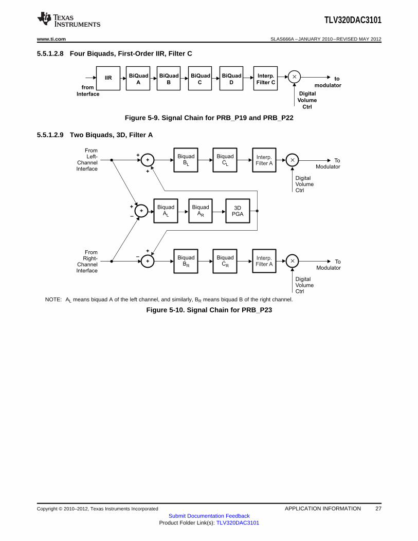
5.5.1.2.8 Four Biquads, First-Order IIR, Filter C
Figure 5-9. Signal Chain for PRB_P19 and PRB_P22
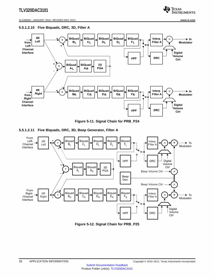
5.5.1.2.9 Two Biquads, 3D, Filter A
NOTE: AL means biquad A of the left channel, and similarly, BR means biquad B of the right channel.
Figure 5-10. Signal Chain for PRB_P23
Copyright © 2010–2012, Texas Instruments Incorporated APPLICATION INFORMATION 27Submit Documentation Feedback
Product Folder Link(s): TLV320DAC3101
BiQuad
AL
Interp.
Filter A
DRCHPF
BiQuad
FL
BiQuad
EL
BiQuad
AR
IIR
Left
3D
PGA
+
+
Interp.
Filter A
DRCHPF
BiQuad
FR
BiQuad
ER
BiQuad
DR
BiQuad
CR
BiQuad
BR
IIR
Right+
+
-
+
-
+
+
from
Left
Channel
Interface
to
Modulator
to
Modulator
Digital
Volume
Ctrl
Digital
Volume
Ctrl
from
Right
Channel
Interface
BiQuad
BL
BiQuad
CL
BiQuad
DL´
´
DRCHPF
3DPGA
+
+
DRCHPF
+
+
–
+
–
+
+
FromLeft-
ChannelInterface
ToModulator
DigitalVolume
Ctrl
BiquadBL
´Biquad
CL
BiquadDL
BiquadAL
BiquadEL
BiquadFL
Interp.Filter A
Interp.Filter A
BiquadAR
FromRight-
ChannelInterface
BiquadBR
BiquadCR
BiquadDR
BiquadER
BiquadFR
ToModulator
DigitalVolumeCtrl
´
+
+
BeepGen.
Beep Volume Ctrl
Beep Volume Ctrl
´
´
IIRLeft
IIRRight
TLV320DAC3101
SLAS666A –JANUARY 2010–REVISED MAY 2012 www.ti.com
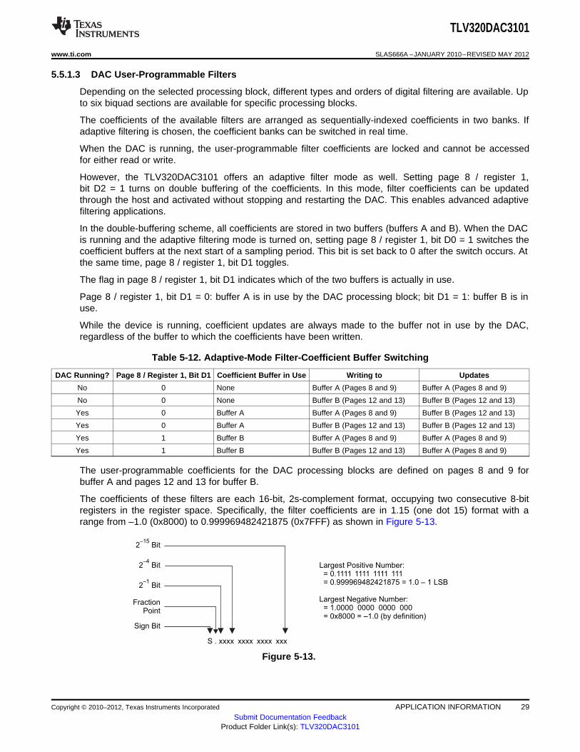
5.5.1.2.10 Five Biquads, DRC, 3D, Filter A
Figure 5-11. Signal Chain for PRB_P24
5.5.1.2.11 Five Biquads, DRC, 3D, Beep Generator, Filter A
Figure 5-12. Signal Chain for PRB_P25
28 APPLICATION INFORMATION Copyright © 2010–2012, Texas Instruments Incorporated
Submit Documentation FeedbackProduct Folder Link(s): TLV320DAC3101
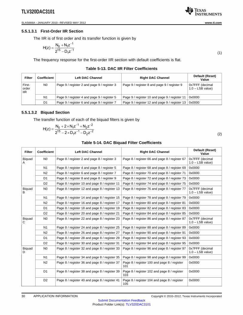
Largest Positive Number:= 0.111 1111 1111 111= 0.999969482421875 = 1.0 – 1 LSB
1
Largest Negative Number:= 1.0000 0000 0000 000= 0x8000 = –1.0 (by definition)
1 1 1
1 1 1
S . xxxx xxxx xxxx xxx. . x x x
Sign Bit
2 Bit–1
2 Bit–4
2 Bit–15
FractionPoint
TLV320DAC3101
www.ti.com SLAS666A –JANUARY 2010–REVISED MAY 2012
5.5.1.3 DAC User-Programmable Filters
Depending on the selected processing block, different types and orders of digital filtering are available. Upto six biquad sections are available for specific processing blocks.
The coefficients of the available filters are arranged as sequentially-indexed coefficients in two banks. Ifadaptive filtering is chosen, the coefficient banks can be switched in real time.
When the DAC is running, the user-programmable filter coefficients are locked and cannot be accessedfor either read or write.
However, the TLV320DAC3101 offers an adaptive filter mode as well. Setting page 8 / register 1,bit D2 = 1 turns on double buffering of the coefficients. In this mode, filter coefficients can be updatedthrough the host and activated without stopping and restarting the DAC. This enables advanced adaptivefiltering applications.
In the double-buffering scheme, all coefficients are stored in two buffers (buffers A and B). When the DACis running and the adaptive filtering mode is turned on, setting page 8 / register 1, bit D0 = 1 switches thecoefficient buffers at the next start of a sampling period. This bit is set back to 0 after the switch occurs. Atthe same time, page 8 / register 1, bit D1 toggles.
The flag in page 8 / register 1, bit D1 indicates which of the two buffers is actually in use.
Page 8 / register 1, bit D1 = 0: buffer A is in use by the DAC processing block; bit D1 = 1: buffer B is inuse.
While the device is running, coefficient updates are always made to the buffer not in use by the DAC,regardless of the buffer to which the coefficients have been written.
Table 5-12. Adaptive-Mode Filter-Coefficient Buffer Switching
DAC Running? Page 8 / Register 1, Bit D1 Coefficient Buffer in Use Writing to Updates
No 0 None Buffer A (Pages 8 and 9) Buffer A (Pages 8 and 9)
No 0 None Buffer B (Pages 12 and 13) Buffer B (Pages 12 and 13)
Yes 0 Buffer A Buffer A (Pages 8 and 9) Buffer B (Pages 12 and 13)
Yes 0 Buffer A Buffer B (Pages 12 and 13) Buffer B (Pages 12 and 13)
Yes 1 Buffer B Buffer A (Pages 8 and 9) Buffer A (Pages 8 and 9)
Yes 1 Buffer B Buffer B (Pages 12 and 13) Buffer A (Pages 8 and 9)
The user-programmable coefficients for the DAC processing blocks are defined on pages 8 and 9 forbuffer A and pages 12 and 13 for buffer B.
The coefficients of these filters are each 16-bit, 2s-complement format, occupying two consecutive 8-bitregisters in the register space. Specifically, the filter coefficients are in 1.15 (one dot 15) format with arange from –1.0 (0x8000) to 0.999969482421875 (0x7FFF) as shown in Figure 5-13.
Figure 5-13.
Copyright © 2010–2012, Texas Instruments Incorporated APPLICATION INFORMATION 29Submit Documentation Feedback
Product Folder Link(s): TLV320DAC3101
10 1
15 11
N N zH(z)
2 D z
-
-
+
=
-
1 20 1 2
15 1 21 2
N 2 N z N zH(z)
2 2 D z D z
- -
- -
+ ´ +
=
- ´ -
TLV320DAC3101
SLAS666A –JANUARY 2010–REVISED MAY 2012 www.ti.com
5.5.1.3.1 First-Order IIR Section
The IIR is of first order and its transfer function is given by
(1)
The frequency response for the first-order IIR section with default coefficients is flat.
Table 5-13. DAC IIR Filter Coefficients
Default (Reset)Filter Coefficient Left DAC Channel Right DAC Channel Value
First- N0 Page 9 / register 2 and page 9 / register 3 Page 9 / register 8 and page 9 / register 9 0x7FFF (decimalorder 1.0 – LSB value)IIR
N1 Page 9 / register 4 and page 9 / register 5 Page 9 / register 10 and page 9 / register 11 0x0000
D1 Page 9 / register 6 and page 9 / register 7 Page 9 / register 12 and page 9 / register 13 0x0000
5.5.1.3.2 Biquad Section
The transfer function of each of the biquad filters is given by
(2)
Table 5-14. DAC Biquad Filter Coefficients
Default (Reset)Filter Coefficient Left DAC Channel Right DAC Channel Value
Biquad N0 Page 8 / register 2 and page 8 / register 3 Page 8 / register 66 and page 8 / register 67 0x7FFF (decimalA 1.0 – LSB value)
N1 Page 8 / register 4 and page 8 / register 5 Page 8 / register 68 and page 8 / register 69 0x0000
N2 Page 8 / register 6 and page 8 / register 7 Page 8 / register 70 and page 8 / register 71 0x0000
D1 Page 8 / register 8 and page 8 / register 9 Page 8 / register 72 and page 8 / register 73 0x0000
D2 Page 8 / register 10 and page 8 / register 11 Page 8 / register 74 and page 8 / register 75 0x0000
Biquad N0 Page 8 / register 12 and page 8 / register 13 Page 8 / register 76 and page 8 / register 77 0x7FFF (decimalB 1.0 – LSB value)
N1 Page 8 / register 14 and page 8 / register 15 Page 8 / register 78 and page 8 / register 79 0x0000
N2 Page 8 / register 16 and page 8 / register 17 Page 8 / register 80 and page 8 / register 81 0x0000
D1 Page 8 / register 18 and page 8 / register 19 Page 8 / register 82 and page 8 / register 83 0x0000
D2 Page 8 / register 20 and page 8 / register 21 Page 8 / register 84 and page 8 / register 85 0x0000
Biquad N0 Page 8 / register 22 and page 8 / register 23 Page 8 / register 86 and page 8 / register 87 0x7FFF (decimalC 1.0 – LSB value)
N1 Page 8 / register 24 and page 8 / register 25 Page 8 / register 88 and page 8 / register 89 0x0000
N2 Page 8 / register 26 and page 8 / register 27 Page 8 / register 90 and page 8 / register 91 0x0000
D1 Page 8 / register 28 and page 8 / register 29 Page 8 / register 92 and page 8 / register 93 0x0000
D2 Page 8 / register 30 and page 8 / register 31 Page 8 / register 94 and page 8 / register 95 0x0000
Biquad N0 Page 8 / register 32 and page 8 / register 33 Page 8 / register 96 and page 8 / register 97 0x7FFF (decimalD 1.0 – LSB value)
N1 Page 8 / register 34 and page 8 / register 35 Page 8 / register 98 and page 8 / register 99 0x0000
N2 Page 8 / register 36 and page 8 / register 37 Page 8 / register 100 and page 8 / register 0x0000101
D1 Page 8 / register 38 and page 8 / register 39 Page 8 / register 102 and page 8 / register 0x0000103
D2 Page 8 / register 40 and page 8 / register 41 Page 8 / register 104 and page 8 / register 0x0000105
30 APPLICATION INFORMATION Copyright © 2010–2012, Texas Instruments Incorporated
Submit Documentation FeedbackProduct Folder Link(s): TLV320DAC3101
0
–10
–20
–30
–40
–50
–60
–70
–80
–90
1 3 4 5 6 72
Mag
nit
ud
e–
dB
Frequency Normalized to fS
DAC Channel Response for Interpolation Filter A(Red Line Corresponds to –65 dB)
TLV320DAC3101
www.ti.com SLAS666A –JANUARY 2010–REVISED MAY 2012
Table 5-14. DAC Biquad Filter Coefficients (continued)
Default (Reset)Filter Coefficient Left DAC Channel Right DAC Channel Value
Biquad N0 Page 8 / register 42 and page 8 / register 43 Page 8 / register 106 and page 8 / register 0x7FFF (decimalE 107 1.0 – LSB value)
N1 Page 8 / register 44 and page 8 / register 45 Page 8 / register 108 and page 8 / register 0x0000109
N2 Page 8 / register 46 and page 8 / register 47 Page 8 / register 110 and page 8 / register 0x0000111
D1 Page 8 / register 48 and page 8 / register 49 Page 8 / register 112 and page 8 / register 0x0000113
D2 Page 8 / register 50 and page 8 / register 51 Page 8 / register 114 and page 8 / register 0x0000115
Biquad N0 Page 8 / register 52 and page 8 / register 53 Page 8 / register 116 and page 8 / register 0x7FFF (decimalF 117 1.0 – LSB value)
N1 Page 8 / register 54 and page 8 / register 55 Page 8 / register 118 and page 8 / register 0x0000119
N2 Page 8 / register 56 and page 8 / register 57 Page 8 / register 120 and page 8 / register 0x0000121
D1 Page 8 / register 58 and page 8 / register 59 Page 8 / register 122 and page 8 / register 0x0000123
D2 Page 8 / register 60 and page 8 / register 61 Page 8 / register 124 and page 8 / register 0x0000125
5.5.1.4 DAC Interpolation Filter Characteristics
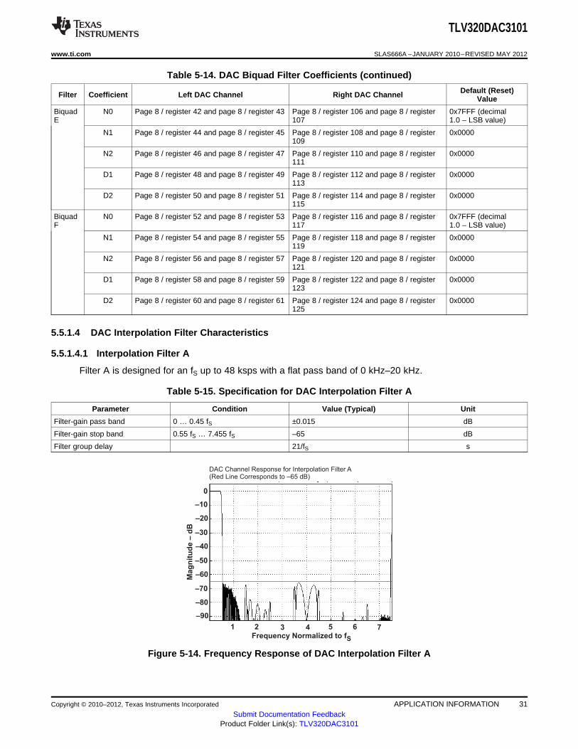
5.5.1.4.1 Interpolation Filter A
Filter A is designed for an fS up to 48 ksps with a flat pass band of 0 kHz–20 kHz.
Table 5-15. Specification for DAC Interpolation Filter A
Parameter Condition Value (Typical) Unit
Filter-gain pass band 0 … 0.45 fS ±0.015 dB
Filter-gain stop band 0.55 fS … 7.455 fS –65 dB
Filter group delay 21/fS s
Figure 5-14. Frequency Response of DAC Interpolation Filter A
Copyright © 2010–2012, Texas Instruments Incorporated APPLICATION INFORMATION 31Submit Documentation Feedback
Product Folder Link(s): TLV320DAC3101
DAC Channel Response for Interpolation Filter B(Red Line Corresponds to –58 dB)
0.5 1 1.5 2 2.5 3 3.5Frequency Normalized to fS
0
–10
–20
–30
–40
–50
–60
–70
–80
Mag
nit
ud
e–
dB
TLV320DAC3101
SLAS666A –JANUARY 2010–REVISED MAY 2012 www.ti.com
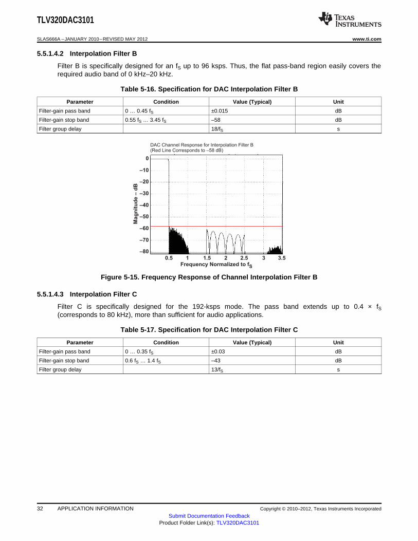
5.5.1.4.2 Interpolation Filter B
Filter B is specifically designed for an fS up to 96 ksps. Thus, the flat pass-band region easily covers therequired audio band of 0 kHz–20 kHz.
Table 5-16. Specification for DAC Interpolation Filter B
Parameter Condition Value (Typical) Unit
Filter-gain pass band 0 … 0.45 fS ±0.015 dB
Filter-gain stop band 0.55 fS … 3.45 fS –58 dB
Filter group delay 18/fS s
Figure 5-15. Frequency Response of Channel Interpolation Filter B
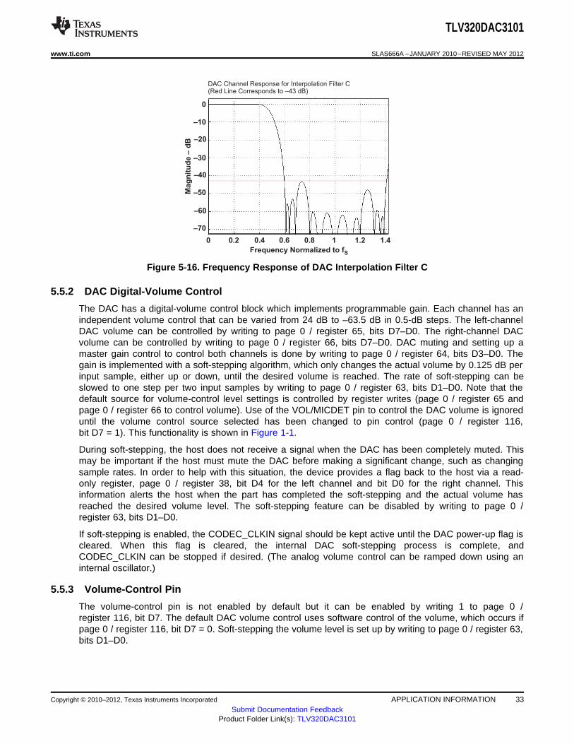
5.5.1.4.3 Interpolation Filter C
Filter C is specifically designed for the 192-ksps mode. The pass band extends up to 0.4 × fS(corresponds to 80 kHz), more than sufficient for audio applications.
Table 5-17. Specification for DAC Interpolation Filter C
Parameter Condition Value (Typical) Unit
Filter-gain pass band 0 … 0.35 fS ±0.03 dB
Filter-gain stop band 0.6 fS … 1.4 fS –43 dB
Filter group delay 13/fS s
32 APPLICATION INFORMATION Copyright © 2010–2012, Texas Instruments Incorporated
Submit Documentation FeedbackProduct Folder Link(s): TLV320DAC3101
0
–10
–20
–30
–40
–50
–60
–70
Mag
nit
ud
e–
dB
0 0.2 0.4 0.6 0.8 1 1.2 1.4
Frequency Normalized to fS
DAC Channel Response for Interpolation Filter C(Red Line Corresponds to –43 dB)
TLV320DAC3101
www.ti.com SLAS666A –JANUARY 2010–REVISED MAY 2012
Figure 5-16. Frequency Response of DAC Interpolation Filter C
5.5.2 DAC Digital-Volume Control
The DAC has a digital-volume control block which implements programmable gain. Each channel has anindependent volume control that can be varied from 24 dB to –63.5 dB in 0.5-dB steps. The left-channelDAC volume can be controlled by writing to page 0 / register 65, bits D7–D0. The right-channel DACvolume can be controlled by writing to page 0 / register 66, bits D7–D0. DAC muting and setting up amaster gain control to control both channels is done by writing to page 0 / register 64, bits D3–D0. Thegain is implemented with a soft-stepping algorithm, which only changes the actual volume by 0.125 dB perinput sample, either up or down, until the desired volume is reached. The rate of soft-stepping can beslowed to one step per two input samples by writing to page 0 / register 63, bits D1–D0. Note that thedefault source for volume-control level settings is controlled by register writes (page 0 / register 65 andpage 0 / register 66 to control volume). Use of the VOL/MICDET pin to control the DAC volume is ignoreduntil the volume control source selected has been changed to pin control (page 0 / register 116,bit D7 = 1). This functionality is shown in Figure 1-1.
During soft-stepping, the host does not receive a signal when the DAC has been completely muted. Thismay be important if the host must mute the DAC before making a significant change, such as changingsample rates. In order to help with this situation, the device provides a flag back to the host via a read-only register, page 0 / register 38, bit D4 for the left channel and bit D0 for the right channel. Thisinformation alerts the host when the part has completed the soft-stepping and the actual volume hasreached the desired volume level. The soft-stepping feature can be disabled by writing to page 0 /register 63, bits D1–D0.
If soft-stepping is enabled, the CODEC_CLKIN signal should be kept active until the DAC power-up flag iscleared. When this flag is cleared, the internal DAC soft-stepping process is complete, andCODEC_CLKIN can be stopped if desired. (The analog volume control can be ramped down using aninternal oscillator.)
5.5.3 Volume-Control Pin
The volume-control pin is not enabled by default but it can be enabled by writing 1 to page 0 /register 116, bit D7. The default DAC volume control uses software control of the volume, which occurs ifpage 0 / register 116, bit D7 = 0. Soft-stepping the volume level is set up by writing to page 0 / register 63,bits D1–D0.
Copyright © 2010–2012, Texas Instruments Incorporated APPLICATION INFORMATION 33Submit Documentation Feedback
Product Folder Link(s): TLV320DAC3101

DAC_L
DAC_R
24 dB to Mute
24 dB to Mute
Digital
Digital
7- Bit ADC
AVDD
P1
AVSS
R1
R2
18 dB to Mute
24 dB to Mute
D-DAC
S
D-DAC
S
Volume LevelRegister Controlled
VolCtl
VolCtl
B0210-08
VREFIN
AVDD
CVOLTone Generator and Mixer Are
NOT Shown
VOL/MICDET
ProcessingBlocks
ProcessingBlocks
TLV320DAC3101
SLAS666A –JANUARY 2010–REVISED MAY 2012 www.ti.com
When the volume-pin function is used, a 7-bit Vol ADC reads the voltage on the VOL/MICDET pin andupdates the digital volume control. (It overwrites the current value of the volume control.) The new volumesetting which has been applied due to a change of voltage on the volume control pin can be read onpage 0 / register 117, bits D6–D0. The 7-bit Vol ADC clock source can be selected on page 0 /register 116, bit D6. The update rate can be programmed on page 0 / register 116, bits D2–D0 for this 7-bit SAR ADC.
The VOL/MICDET pin gain mapping is shown in Table 5-18.
Table 5-18. VOL/MICDET Pin Gain Mapping
VOL/MICDET PIN SAR OUTPUT DIGITAL GAIN APPLIED
0 18 dB
1 17.5 dB
2 17 dB
: :
35 0.5 dB
36 0.0 dB
37 –0.5 dB
: :
89 –26.5 dB
90 –27 dB
91 –28 dB
: :
125 –62 dB
126 –63 dB
127 Mute
The VOL/MICDET pin connection and functionality are shown in Figure 5-17.
Figure 5-17. Digital Volume Controls for Beep Generator and DAC Play Data
34 APPLICATION INFORMATION Copyright © 2010–2012, Texas Instruments Incorporated
Submit Documentation FeedbackProduct Folder Link(s): TLV320DAC3101
10 1
HPF 15 11
N N zH (z)
2 D z
-
-
+
=
-
10 1
LPF 15 11
N N zH (z)
2 D z
-
-
+
=
-
TLV320DAC3101
www.ti.com SLAS666A –JANUARY 2010–REVISED MAY 2012
As shown in Table 5-18, the VOL/MICDET pin has a range of volume control from 18 dB down to –63 dB,and mute. However, if less maximum gain is required, then a smaller range of voltage should be appliedto the VOL/MICDET pin. This can be done by increasing the value of R2 relative to the value of (P1 + R1),so that more voltage is available at the bottom of P1. The circuit should also be designed such that for thevalues of R1, R2, and P1 chosen, the maximum voltage (top of the potentiometer or VOL/MICDET pin)does not exceed AVDD/2 (see Figure 5-17). The recommended values for R1, R2, and P1 for severalmaximum gains are shown in Table 5-19.
Table 5-19. VOL/MICDET Pin Gain Scaling
ADC VOLTAGER1 P1 R2 DIGITAL GAIN RANGEfor AVDD = 3.3 V(kΩ) (kΩ) (kΩ) (dB)(V)
25 25 0 0 V to 1.65 V 18 dB to –63 dB
33 25 7.68 0.386 V to 1.642 V 3 dB to –63 dB
34.8 25 9.76 0.463 V to 1.649 V 0 dB to –63 dB
5.5.4 Dynamic Range Compression
Typical music signals are characterized by crest factors, the ratio of peak signal power to average signalpower, of 12 dB or more. To avoid audible distortions due to clipping of peak signals, the gain of the DACchannel must be adjusted so as not to cause hard clipping of peak signals. As a result, during nominalperiods, the applied gain is low, causing the perception that the signal is not loud enough. To overcomethis problem, dynamic range conpression (DRC) in the TLV320DAC3101 continuously monitors the outputof the DAC digital volume control to detect its power level relative to 0 dBFS. When the power level is low,DRC increases the input signal gain to make it sound louder. At the same time, if a peaking signal isdetected, it autonomously reduces the applied gain to avoid hard clipping. This results in sounds morepleasing to the ear as well as sounding louder during nominal periods.
The DRC functionality in the TLV320DAC3101 is implemented by a combination of processing blocks inthe DAC channel as described in Section 5.5.1.2.
DRC can be disabled by writing to page 0 / register 68, bits D6–D5.
DRC typically works on the filtered version of the input signal. The input signals have no audio informationat dc and extremely low frequencies; however, they can significantly influence the energy estimationfunction in the dynamic range compressor (the DRC). Also, most of the information about signal energy isconcentrated in the low-frequency region of the input signal.
To estimate the energy of the input signal, the signal is first fed to the DRC high-pass filter and then to theDRC low-pass filter. These filters are implemented as first-order IIR filters given by
(3)
(4)
The coefficients for these filters are 16 bits wide in 2s-complement format and are user-programmablethrough register write as given in Table 5-20.
Copyright © 2010–2012, Texas Instruments Incorporated APPLICATION INFORMATION 35Submit Documentation Feedback
Product Folder Link(s): TLV320DAC3101
TLV320DAC3101
SLAS666A –JANUARY 2010–REVISED MAY 2012 www.ti.com
Table 5-20. The DRC HPF and LPF Coefficients
Coefficient Location
HPF N0 C71 page 9 / register 14 and page 9 / register 15
HPF N1 C72 page 9 / register 16 and page 9 / register 17
HPF D1 C73 page 9 / register 18 and page 9 / register 19
LPF N0 C74 page 9 / register 20 and page 9 / register 21
LPF N1 C75 page 9 / register 22 and page 9 / register 23
LPF D1 C76 page 9 / register 24 and page 9 / register 25
The default values of these coefficients implement a high-pass filter with a cutoff at 0.00166 × DAC_fS,and a low-pass filter with a cutoff at 0.00033 × DAC_fS.
The output of the DRC high-pass filter is fed to the processing block selected for the DAC channel. Theabsolute value of the DRC LPF filter is used for energy estimation within the DRC.
The gain in the DAC digital volume control is controlled by page 0 / register 65 and page 0 / register 66.When the DRC is enabled, the applied gain is a function of the digital volume control register setting andthe output of the DRC.
The DRC parameters are described in sections that follow.
5.5.4.1 DRC Threshold
DRC threshold represents the level of the DAC playback signal at which the gain compression becomesactive. The output of the digital volume control in the DAC is compared with the set threshold. Thethreshold value is programmable by writing to page 0 / register 68, bits D4–D2. The threshold value canbe adjusted between –3 dBFS and –24 dBFS in steps of 3 dB. Keeping the DRC threshold value too highmay not leave enough time for the DRC block to detect peaking signals, and can cause excessivedistortion at the outputs. Keeping the DRC threshold value too low can limit the perceived loudness of theoutput signal.
The recommended DRC threshold value is –24 dB.
When the output signal exceeds the set DRC threshold, the interrupt flag bits at page 0 / register 44,bits D3–D2 are updated. These flag bits are sticky in nature, and are reset only after they are read backby the user. The non-sticky versions of the interrupt flags are also available at page 0 / register 46,bits D3–D2.
5.5.4.2 DRC Hysteresis
DRC hysteresis is programmable by writing to page 0 / register 68, bits D1–D0. These bits can beprogrammed to represent values between 0 dB and 3 dB in steps of 1 dB. It is a programmable windowaround the programmed DRC threshold that must be exceeded for the disabled DRC to become enabled,or the enabled DRC to become disabled. For example, if the DRC threshold is set to –12 dBFS and theDRC hysteresis is set to 3 dB, then if the gain compression in the DRC is inactive, the output of the DACdigital volume control must exceed –9 dBFS before gain compression due to the DRC is activated.Similarly, when the gain compression in the DRC is active, the output of the DAC digital volume controlmust fall below –15 dBFS for gain compression in the DRC to be deactivated. The DRC hysteresis featureprevents the rapid activation and de-activation of gain compression in the DRC in cases when the outputof the DAC digital volume control rapidly fluctuates in a narrow region around the programmed DRCthreshold. By programming the DRC hysteresis as 0 dB, the hysteresis action is disabled.
The recommended value of DRC hysteresis is 3 dB.
5.5.4.3 DRC Hold Time
DRC hold time is intended to slow the start of decay for a specified period of time in response to adecrease in energy level. To minimize audible artifacts, it is recommended to set the DRC hold time to 0through programming page 0 / register 69, bits D6–D3 = 0000.
36 APPLICATION INFORMATION Copyright © 2010–2012, Texas Instruments Incorporated
Submit Documentation FeedbackProduct Folder Link(s): TLV320DAC3101
TLV320DAC3101
www.ti.com SLAS666A –JANUARY 2010–REVISED MAY 2012
5.5.4.4 DRC Attack Rate
When the output of the DAC digital volume control exceeds the programmed DRC threshold, the gainapplied in the DAC digital volume control is progressively reduced to avoid the signal from saturating thechannel. This process of reducing the applied gain is called attack. To avoid audible artifacts, the gain isreduced slowly with a rate equaling the attack rate, programmable via page 0 / register 70, bits D7–D4.Attack rates can be programmed from 4-dB gain change per sample period to 1.2207e–5-dB gain changeper sample period.
Attack rates should be programmed such that before the output of the DAC digital volume control can clip,the input signal should be sufficiently attenuated. High attack rates can cause audible artifacts, and too-slow attack rates may not be able to prevent the input signal from clipping.
The recommended DRC attack rate value is 1.9531e–4 dB per sample period.
5.5.4.5 DRC Decay Rate
When the DRC detects a reduction in output signal swing beyond the programmed DRC threshold, theDRC enters a decay state, where the applied gain in the digital-volume control is gradually increased toprogrammed values. To avoid audible artifacts, the gain is slowly increased with a rate equal to the decayrate programmed through page 0 / register 70, bits D3–D0. The decay rates can be programmed from1.5625e–3 dB per sample period to 4.7683e–7 dB per sample period. If the decay rates are programmedtoo high, then sudden gain changes can cause audible artifacts. However, if it is programmed too slow,then the output may be perceived as too low for a long time after the peak signal has passed.
The recommended value of DRC decay rate is 2.4414e–5 dB per sample period.
Copyright © 2010–2012, Texas Instruments Incorporated APPLICATION INFORMATION 37Submit Documentation Feedback
Product Folder Link(s): TLV320DAC3101
Micbias
Micdet
MICBIAS
HPR
HPL
VOL/MICDET
TLV320DAC3101
SLAS666A –JANUARY 2010–REVISED MAY 2012 www.ti.com
5.5.4.6 Example Setup for DRC
• Digital Vol gain = 12 dB• Threshold = –24 dB• Hysteresis = 3 dB• Hold time = 0 ms• Attack rate = 1.9531e–4 dB per sample period• Decay rate = 2.4414e–5 dB per sample period
Script# Select Page 0w 30 00 00# DAC => 12 db gain leftw 30 41 18# DAC => 12 db gain rightw 30 42 18# DAC => DRC Enabled for both channels, Threshold = -24 db, Hysteresis = 3 dBw 30 44 7F# DRC Hold = 0 ms, Rate of Changes of Gain = 0.5 dB/Fs'w 30 45 00# Attack Rate = 1.9531e-4 dB/Frame , DRC Decay Rate =2.4414e-5 dB/Framew 30 46 B6# Select Page 9w 30 00 09# DRC HPFw 30 0E 7F AB 80 55 7F 56# DRC LPF W 30 14 00 11 00 11 7F DE
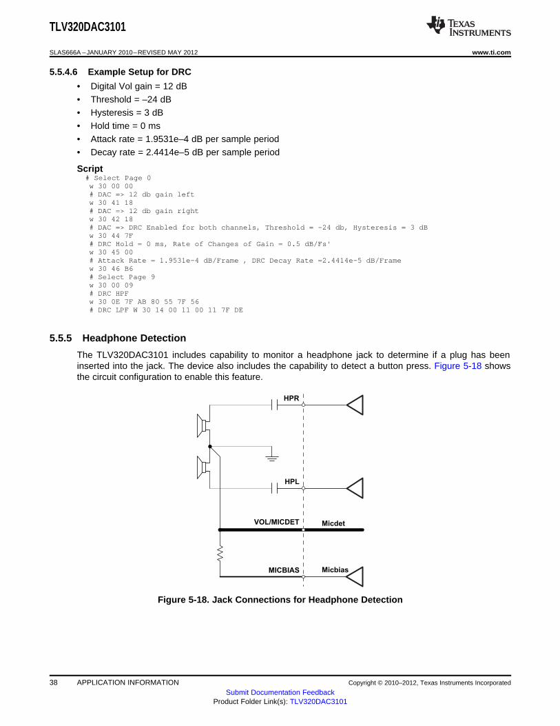
5.5.5 Headphone Detection
The TLV320DAC3101 includes capability to monitor a headphone jack to determine if a plug has beeninserted into the jack. The device also includes the capability to detect a button press. Figure 5-18 showsthe circuit configuration to enable this feature.
Figure 5-18. Jack Connections for Headphone Detection
38 APPLICATION INFORMATION Copyright © 2010–2012, Texas Instruments Incorporated
Submit Documentation FeedbackProduct Folder Link(s): TLV320DAC3101
TLV320DAC3101
www.ti.com SLAS666A –JANUARY 2010–REVISED MAY 2012
Headphone detection is enabled by programming page 0 / register 67, bit D7. In order to avoid falsedetections due to mechanical vibrations in headset jacks or microphone buttons, a debounce function isprovided for glitch rejection. For the case of headset insertion, a debounce function with a range of 32 msto 512 ms is provided. This can be programmed via page 0 / register 67, bits D4–D2. For improved button-press detection, the debounce function has a range of 8 ms to 32 ms by programming page 0 / register67, bits D1–D0.
The TLV320DAC3101 also provides feedback to the user through register-readable flags as well as aninterrupt on the I/O pins when a button press or a headset insertion/removal event is detected. The valuein page 0 / register 46, bits D5–D4 provides the instantaneous state of button press and headset insertion.Page 0 / register 44, bit D5 is a sticky (latched) flag that is set when the button-press event is detected.Page 0 / register 44, bit D4 is a sticky flag which is set when the headset insertion or removal event isdetected. These sticky flags are set by the event occurrence, and are reset only when read. This requirespolling page 0 / register 44. To avoid polling and the associated overhead, the TLV320DAC3101 alsoprovides an interrupt feature, whereby events can trigger the INT1 and/or INT2 interrupts. These interruptevents can be routed to one of the digital output pins. See Section 5.5.6 for details.
The TLV320DAC3101 not only detects a headset insertion event, but also is able to distinguish betweenthe different headsets inserted, such as stereo headphones or cellular headphones. After the headset-detection event, the user can read page 0 / register 67, bits D6–D5 to determine the type of headsetinserted.
Table 5-21. Headphone-Detection Block Registers
Register Description
Page 0 / register 67, bit D1 Headset-detection enable/disable
Page 0 / register 67, bits D4–D2 Debounce programmability for headset detection
Page 0 / register 67, bits D1–D0 Debounce programmability for button press
Page 0 / register 44, bit D5 Sticky flag for button-press event
Page 0 / register 44, bit D4 Sticky flag for headset-insertion or -removal event
Page 0/ register 46, bit D5 Status flag for button-press event
Page 0 / register 46, bit D4 Status flag for headset insertion and removal
Page 0 / register 67, bits D6–D5 Flags for type of headset detected
The headset detection block requires AVDD to be powered. The headset detection feature in theTLV320DAC3101 is achieved with very low power overhead, requiring less than 20 μA of additionalcurrent from the AVDD supply.
5.5.6 Interrupts
Some specific events in the TLV320DAC3101 which may require host processor intervention, can be usedto trigger interrupts to the host processor. This avoids polling the status-flag registers continuously. TheTLV320DAC3101 has two defined interrupts, INT1 and INT2, that can be configured by programmingpage 0 / register 48 and page 0 / register 49. A user can configure interrupts INT1 and INT2 to betriggered by one or many events, such as:• Headset detection• Button press• DAC DRC signal exceeding threshold• Overcurrent condition in headphone drivers/speaker drivers• Data overflow in the DAC processing blocks and filters
Each of these INT1 and INT2 interrupts can be routed to pin GPIO1. These interrupt signals can either beconfigured as a single pulse or a series of pulses by programming page 0 / register 48, bit D0 andpage 0 / register 49, bit D0. If the user configures the interrupts as a series of pulses, the events triggerthe start of pulses that stop when the flag registers in page 0 / register 44, page 0 / register 45, andpage 0 / register 50 are read by the user to determine the cause of the interrupt.
Copyright © 2010–2012, Texas Instruments Incorporated APPLICATION INFORMATION 39Submit Documentation Feedback
Product Folder Link(s): TLV320DAC3101
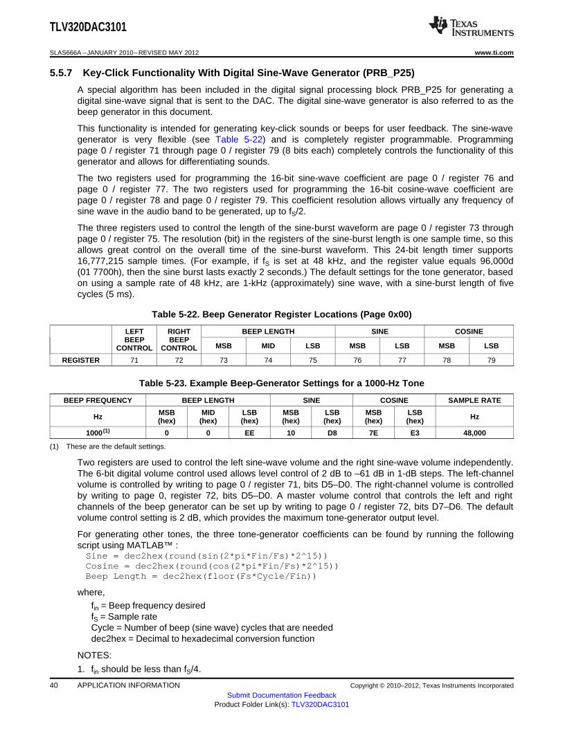
TLV320DAC3101
SLAS666A –JANUARY 2010–REVISED MAY 2012 www.ti.com
5.5.7 Key-Click Functionality With Digital Sine-Wave Generator (PRB_P25)
A special algorithm has been included in the digital signal processing block PRB_P25 for generating adigital sine-wave signal that is sent to the DAC. The digital sine-wave generator is also referred to as thebeep generator in this document.
This functionality is intended for generating key-click sounds or beeps for user feedback. The sine-wavegenerator is very flexible (see Table 5-22) and is completely register programmable. Programmingpage 0 / register 71 through page 0 / register 79 (8 bits each) completely controls the functionality of thisgenerator and allows for differentiating sounds.
The two registers used for programming the 16-bit sine-wave coefficient are page 0 / register 76 andpage 0 / register 77. The two registers used for programming the 16-bit cosine-wave coefficient arepage 0 / register 78 and page 0 / register 79. This coefficient resolution allows virtually any frequency ofsine wave in the audio band to be generated, up to fS/2.
The three registers used to control the length of the sine-burst waveform are page 0 / register 73 throughpage 0 / register 75. The resolution (bit) in the registers of the sine-burst length is one sample time, so thisallows great control on the overall time of the sine-burst waveform. This 24-bit length timer supports16,777,215 sample times. (For example, if fS is set at 48 kHz, and the register value equals 96,000d(01 7700h), then the sine burst lasts exactly 2 seconds.) The default settings for the tone generator, basedon using a sample rate of 48 kHz, are 1-kHz (approximately) sine wave, with a sine-burst length of fivecycles (5 ms).
Table 5-22. Beep Generator Register Locations (Page 0x00)
LEFT RIGHT BEEP LENGTH SINE COSINEBEEP BEEP
MSB MID LSB MSB LSB MSB LSBCONTROL CONTROL
REGISTER 71 72 73 74 75 76 77 78 79
Table 5-23. Example Beep-Generator Settings for a 1000-Hz Tone
BEEP FREQUENCY BEEP LENGTH SINE COSINE SAMPLE RATE
MSB MID LSB MSB LSB MSB LSBHz Hz(hex) (hex) (hex) (hex) (hex) (hex) (hex)
1000 (1) 0 0 EE 10 D8 7E E3 48,000
(1) These are the default settings.
Two registers are used to control the left sine-wave volume and the right sine-wave volume independently.The 6-bit digital volume control used allows level control of 2 dB to –61 dB in 1-dB steps. The left-channelvolume is controlled by writing to page 0 / register 71, bits D5–D0. The right-channel volume is controlledby writing to page 0, register 72, bits D5–D0. A master volume control that controls the left and rightchannels of the beep generator can be set up by writing to page 0 / register 72, bits D7–D6. The defaultvolume control setting is 2 dB, which provides the maximum tone-generator output level.
For generating other tones, the three tone-generator coefficients can be found by running the followingscript using MATLAB™ :Sine = dec2hex(round(sin(2*pi*Fin/Fs)*2^15))Cosine = dec2hex(round(cos(2*pi*Fin/Fs)*2^15))Beep Length = dec2hex(floor(Fs*Cycle/Fin))
where,fin = Beep frequency desiredfS = Sample rateCycle = Number of beep (sine wave) cycles that are neededdec2hex = Decimal to hexadecimal conversion function
NOTES:
1. fin should be less than fS/4.
40 APPLICATION INFORMATION Copyright © 2010–2012, Texas Instruments Incorporated
Submit Documentation FeedbackProduct Folder Link(s): TLV320DAC3101
TLV320DAC3101
www.ti.com SLAS666A –JANUARY 2010–REVISED MAY 2012
2. For the sine and cosine values, if the number of bits is less than the full 16-bit value, then the unusedMSBs must be written as 0s.
3. For the beep-length values, if number of bits is less than the full 24-bit value, then the unused MSBsmust be written as 0s.
Following the beep-volume control is a digital mixer that mixes in a playback data stream whose level hasalready been set by the DAC volume control. Therefore, once the key-click volume level is set, the key-click volume is not affected by the DAC volume control, which is the main control available to the enduser. This functionality is shown in Figure 1-1.
Following the DAC, the signal can be further scaled by the analog output volume control and power-amplifier level control.
The beep generator is used for the key-click function. A single beep is generated by writing to page 0 /register 71, bit D7. After the programmed beep length has finished, register 71, bit D7 is reset back tozero.
5.5.8 Programming DAC Digital Filter Coefficients
The digital filter coefficients must be programmed through the I2C interface. All digital filtering for the DACsignal path must be loaded into the RAM before the DAC is powered on. (Note that default ALLPASS filtercoefficients for programmable biquads are located in boot ROM. The boot ROM automatically loads thedefault values into the RAM following a hardware reset (toggling the RESET pin) or after a software reset.After resetting the device, loading boot ROM coefficients into the digital filters requires 100 μs ofprogramming time. During this time, reading or writing to page 8 through page 15 for updating DAC filtercoefficient values is not permitted. (The DAC should not be powered up until after all of the DACconfigurations have been done by the system microprocessor.)
5.5.9 Updating DAC Digital Filter Coefficients During PLAY
When it is required to update the DAC digital filter coefficients or beep generator during play, care must betaken to avoid click and pop noise or even a possible oscillation noise. These artifacts can occur if theDAC coefficients are updated without following the proper update sequence. The correct sequence isshown in Figure 5-19. The values for times listed in Figure 5-19 are conservative and should be used forsoftware purposes.
There is also an adaptive mode, in which DAC coefficients can be updated while the DAC is on. Fordetails, see Section 5.5.1.3.
Copyright © 2010–2012, Texas Instruments Incorporated APPLICATION INFORMATION 41Submit Documentation Feedback
Product Folder Link(s): TLV320DAC3101
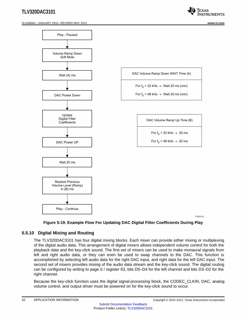
Play - Paused
DAC Power Down
UpdateDigital FilterCoefficients
DAC Power UP
Wait 20 ms
Volume Ramp DownSoft Mute
Restore PreviousVolume Level (Ramp)
in (B) ms
Play - Continue
Wait (A) ms
For f = 32 kHzS ® Wait 25 ms (min)
For f = 48 kHz Wait 20 ms (min)S ®
For = 32 kHz ®f 25 ms
For f = 48 kHz 20 ms
S
S ®
DAC Volume Ramp Down WAIT Time (A)
DAC Volume Ramp Up Time (B)
F0024-02
TLV320DAC3101
SLAS666A –JANUARY 2010–REVISED MAY 2012 www.ti.com
Figure 5-19. Example Flow For Updating DAC Digital Filter Coefficients During Play
5.5.10 Digital Mixing and Routing
The TLV320DAC3101 has four digital mixing blocks. Each mixer can provide either mixing or multiplexingof the digital audio data. This arrangement of digital mixers allows independent volume control for both theplayback data and the key-click sound. The first set of mixers can be used to make monaural signals fromleft and right audio data, or they can even be used to swap channels to the DAC. This function isaccomplished by selecting left audio data for the right DAC input, and right data for the left DAC input. Thesecond set of mixers provides mixing of the audio data stream and the key-click sound. The digital routingcan be configured by writing to page 0 / register 63, bits D5–D4 for the left channel and bits D3–D2 for theright channel.
Because the key-click function uses the digital signal-processing block, the CODEC_CLKIN, DAC, analogvolume control, and output driver must be powered on for the key-click sound to occur.
42 APPLICATION INFORMATION Copyright © 2010–2012, Texas Instruments Incorporated
Submit Documentation FeedbackProduct Folder Link(s): TLV320DAC3101
TLV320DAC3101
www.ti.com SLAS666A –JANUARY 2010–REVISED MAY 2012
5.5.11 Analog Audio Routing
The TLV320DAC3101 has the capability to route the DAC output to either the headphone or the speakeroutput. If desirable, both output drivers can be operated at the same time while playing at different volumelevels. The TLV320DAC3101 provides various digital routing capabilities, allowing digital mixing or evenchannel swapping in the digital domain. All analog outputs other than the selected ones can be powereddown for optimal power consumption.
5.5.11.1 Analog Output Volume Control
The output volume control can be used to fine-tune the level of the mixer amplifier signal supplied to theheadphone driver or the speaker driver. This architecture supports separate and concurrent volume levelsfor each of the four output drivers. This volume control can also be used as part of the output pop-noisereduction scheme. This feature is available even if the DAC is powered down.
5.5.11.2 Headphone Analog Output Volume Control
For the headphone outputs, the analog volume control has a range from 0 dB to –78 dB in 0.5-dB stepsfor most of the useful range plus mute, which is shown in Table 5-24. This volume control includes soft-stepping logic. Routing the left-channel DAC output signal to the left-channel analog volume control isdone by writing to page 1 / register 35, bit D6. Routing the right-channel DAC output signal to the right-channel analog volume control is done by writing to page 1 / register 35, bit D2.
Changing the left-channel analog volume for the headphone is controlled by writing to page 1 / register 36,bits D6–D0. Changing the right-channel analog volume for the headphone is controlled by writing topage 1 / register 37, bits D6–D0. Routing the signal from the output of the left-channel analog volumecontrol to the input of the left-channel headphone power amplifier is done by writing to page 1 /register 36, bit D7. Routing the signal from the output of the right-channel analog volume control to theinput of the right-channel headphone power amplifier is done by writing to page 1 / register 37, bit D7.
The analog volume-control soft-stepping time is based on the setting in page 0 / register 63, bits D1–D0.
Copyright © 2010–2012, Texas Instruments Incorporated APPLICATION INFORMATION 43Submit Documentation Feedback
Product Folder Link(s): TLV320DAC3101
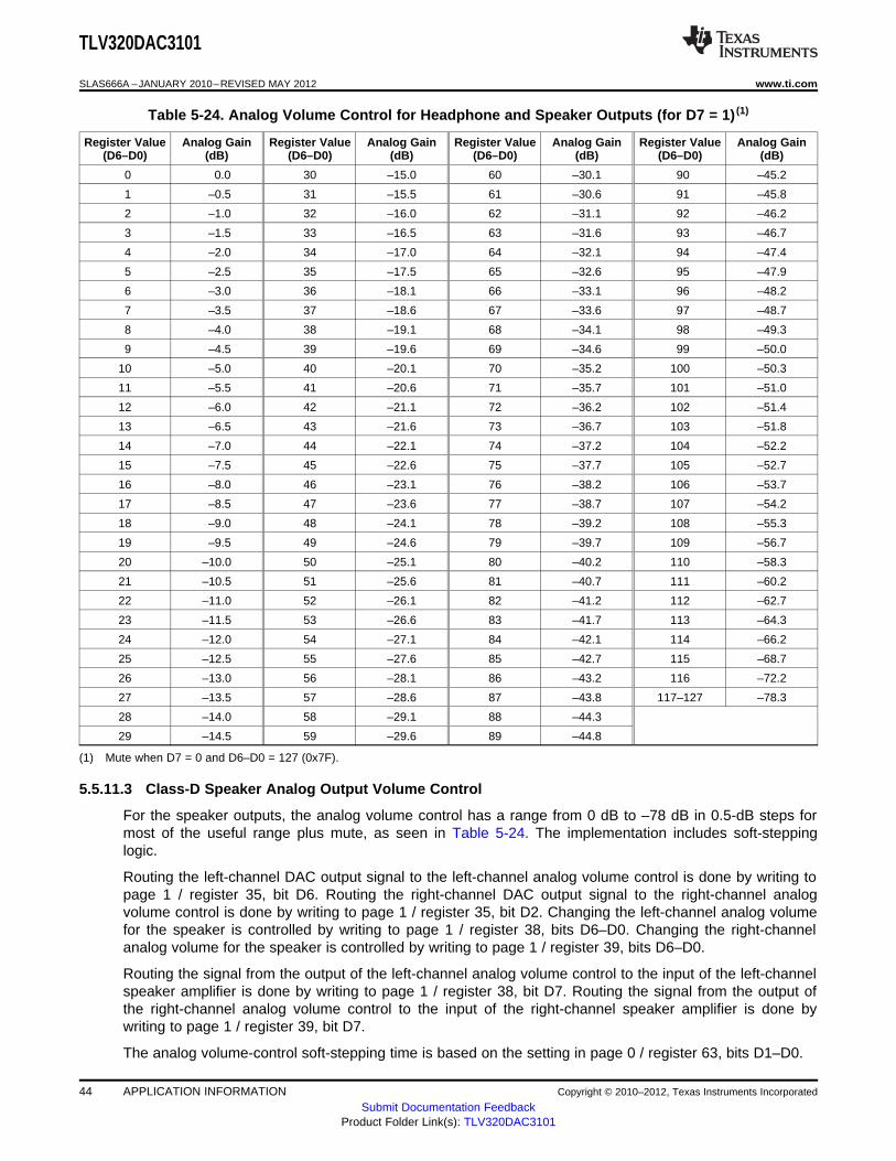
TLV320DAC3101
SLAS666A –JANUARY 2010–REVISED MAY 2012 www.ti.com
Table 5-24. Analog Volume Control for Headphone and Speaker Outputs (for D7 = 1) (1)
Register Value Analog Gain Register Value Analog Gain Register Value Analog Gain Register Value Analog Gain(D6–D0) (dB) (D6–D0) (dB) (D6–D0) (dB) (D6–D0) (dB)
0 0.0 30 –15.0 60 –30.1 90 –45.2
1 –0.5 31 –15.5 61 –30.6 91 –45.8
2 –1.0 32 –16.0 62 –31.1 92 –46.2
3 –1.5 33 –16.5 63 –31.6 93 –46.7
4 –2.0 34 –17.0 64 –32.1 94 –47.4
5 –2.5 35 –17.5 65 –32.6 95 –47.9
6 –3.0 36 –18.1 66 –33.1 96 –48.2
7 –3.5 37 –18.6 67 –33.6 97 –48.7
8 –4.0 38 –19.1 68 –34.1 98 –49.3
9 –4.5 39 –19.6 69 –34.6 99 –50.0
10 –5.0 40 –20.1 70 –35.2 100 –50.3
11 –5.5 41 –20.6 71 –35.7 101 –51.0
12 –6.0 42 –21.1 72 –36.2 102 –51.4
13 –6.5 43 –21.6 73 –36.7 103 –51.8
14 –7.0 44 –22.1 74 –37.2 104 –52.2
15 –7.5 45 –22.6 75 –37.7 105 –52.7
16 –8.0 46 –23.1 76 –38.2 106 –53.7
17 –8.5 47 –23.6 77 –38.7 107 –54.2
18 –9.0 48 –24.1 78 –39.2 108 –55.3
19 –9.5 49 –24.6 79 –39.7 109 –56.7
20 –10.0 50 –25.1 80 –40.2 110 –58.3
21 –10.5 51 –25.6 81 –40.7 111 –60.2
22 –11.0 52 –26.1 82 –41.2 112 –62.7
23 –11.5 53 –26.6 83 –41.7 113 –64.3
24 –12.0 54 –27.1 84 –42.1 114 –66.2
25 –12.5 55 –27.6 85 –42.7 115 –68.7
26 –13.0 56 –28.1 86 –43.2 116 –72.2
27 –13.5 57 –28.6 87 –43.8 117–127 –78.3
28 –14.0 58 –29.1 88 –44.3
29 –14.5 59 –29.6 89 –44.8
(1) Mute when D7 = 0 and D6–D0 = 127 (0x7F).
5.5.11.3 Class-D Speaker Analog Output Volume Control
For the speaker outputs, the analog volume control has a range from 0 dB to –78 dB in 0.5-dB steps formost of the useful range plus mute, as seen in Table 5-24. The implementation includes soft-steppinglogic.
Routing the left-channel DAC output signal to the left-channel analog volume control is done by writing topage 1 / register 35, bit D6. Routing the right-channel DAC output signal to the right-channel analogvolume control is done by writing to page 1 / register 35, bit D2. Changing the left-channel analog volumefor the speaker is controlled by writing to page 1 / register 38, bits D6–D0. Changing the right-channelanalog volume for the speaker is controlled by writing to page 1 / register 39, bits D6–D0.
Routing the signal from the output of the left-channel analog volume control to the input of the left-channelspeaker amplifier is done by writing to page 1 / register 38, bit D7. Routing the signal from the output ofthe right-channel analog volume control to the input of the right-channel speaker amplifier is done bywriting to page 1 / register 39, bit D7.
The analog volume-control soft-stepping time is based on the setting in page 0 / register 63, bits D1–D0.
44 APPLICATION INFORMATION Copyright © 2010–2012, Texas Instruments Incorporated
Submit Documentation FeedbackProduct Folder Link(s): TLV320DAC3101
TLV320DAC3101
www.ti.com SLAS666A –JANUARY 2010–REVISED MAY 2012
5.5.12 Analog Outputs
Various analog routings are supported for playback. All the options can be conveniently viewed on thefunctional block diagram, Figure 1-1.
5.5.12.1 Headphone Drivers
The TLV320DAC3101 features a stereo headphone driver (HPL and HPR) that can deliver up to 30 mWper channel, at 3.3-V supply voltage, into a 16-Ω load. The headphones are used in a single-endedconfiguration where an ac-coupling capacitor (dc-blocking) is connected between the device output pinsand the headphones. The headphone driver also supports 32-Ω and 10-kΩ loads without changing anycontrol register settings.
The headphone drivers can be configured to optimize the power consumption in the lineout-drive mode bywriting 11 to page 1 / register 44, bits D2–D1.
The output common mode of the headphone/lineout drivers can be programmed to 1.35 V, 1.5 V, 1.65 V,or 1.8 V by setting page 1 / register 31, bits D4–D3. The common-mode voltage should be set ≤ AVDD/2.
The left headphone driver can be powered on by writing to page 1 / register 31, bit D7. The rightheadphone driver can be powered on by writing to page 1 / register 31, bit D6. The left-output driver gaincan be controlled by writing to page 1 / register 40, bits D6–D3, and it can be muted by writing to page 1 /register 40, bit D2. The right-output driver gain can be controlled by writing to page 1 / register 41,bits D6–D3, and it can be muted by writing to page 1 / register 41, bit D2.
The TLV320DAC3101 has a short-circuit protection feature for the headphone drivers, which is alwaysenabled to provide protection. The output condition of the headphone driver during short circuit can beprogrammed by writing to page 1 / register 31, bit D1. If D1 = 0 when a short circuit is detected, the devicelimits the maximum current to the load. If D1 = 1 when a short circuit is detected, the device powers downthe output driver. The default condition for headphones is the current-limiting mode. In case of a shortcircuit on either channel, the output is disabled and a status flag is provided as read-only bits on page 1 /register 31, bit D0. If shutdown mode is enabled, then as soon as the short circuit is detected, page 1 /register 31, bit D7 (for HPL) and/or page 1 / register 31, bit D6 (for HPR) clears automatically. Next, thedevice requires a reset to re-enable the output stage. Resetting can be done in two ways. First, the devicemaster reset can be used, which requires either toggling the RESET pin or using the software reset. Ifmaster reset is used, it resets all of the registers. Second, a dedicated headphone power-stage reset canalso be used to re-enable the output stage, and that keeps all of the other device settings. The headphonepower stage reset is done by setting page 1 / register 31, bit D7 for HPL and by setting page 1 /register 31, bit D6 for HPR. If the fault condition has been removed, then the device returns to normaloperation. If the fault is still present, then another shutdown occurs. Repeated resetting (more than threetimes) is not recommended, as this could lead to overheating.
5.5.12.2 Speaker Drivers
The TLV320DAC3101 has an integrated class-D stereo speaker driver (SPLP/SPLM and SPRP/SPRM)capable of driving an 8-Ω differential load. The speaker driver can be powered directly from the batterysupply (2.7 V to 5.5 V) on the SPLVDD and SPRVDD pins; however, the voltage (including spike voltage)must be limited below the absolute-maximum voltage of 6 V.
The speaker driver is capable of supplying 400 mW per channel with a 3.6-V power supply. Through theuse of digital mixing, the device can connect one or both digital audio playback data channels to eitherspeaker driver; this also allows digital channel swapping if needed.
The left class-D speaker driver can be powered on by writing to page 1 / register 32, bit D7. The rightclass-D speaker driver can be powered on by writing to page 1 / register 32, bit D6. The left-output drivergain can be controlled by writing to page 1 / register 42, bits D4–D3, and it can be muted by writing topage 1 / register 42, bit D2. The right-output driver gain can be controlled by writing to page 1 /register 43, bits D4–D3, and it can be muted by writing to page 1 / register 43, bit D2.
Copyright © 2010–2012, Texas Instruments Incorporated APPLICATION INFORMATION 45Submit Documentation Feedback
Product Folder Link(s): TLV320DAC3101
TLV320DAC3101
SLAS666A –JANUARY 2010–REVISED MAY 2012 www.ti.com
The TLV320DAC3101 has a short-circuit protection feature for the speaker drivers that is always enabledto provide protection. If the output is shorted, the output stage shuts down on the overcurrent condition.(Current limiting is not an available option for the higher-current speaker-driver output stage.) In case of ashort circuit on either channel, the output is disabled and a status flag is provided as a read-only bit onpage 1 / register 32, bit D0.
If shutdown occurs due to an overcurrent condition, then the device requires a reset to re-enable theoutput stage. Resetting can be done in two ways. First, the device master reset can be used, whichrequires either toggling the RESET pin or using the software reset. If master reset is used, it resets all ofthe registers. Second, a dedicated speaker power-stage reset can be used that keeps all of the otherdevice settings. The speaker power-stage reset is done by setting page 1 / register 32, bit D7 for SPLPand SPLM and by setting page 1 / register 32, bit D6 for SPRP and SPRM. If the fault condition has beenremoved, then the device returns to normal operation. If the fault is still present, then another shutdownoccurs. Repeated resetting (more than three times) is not recommended, as this could lead tooverheating.
To minimize battery current leakage, the SPLVDD and SPRVDD voltage levels should not be lessthan the AVDD voltage level.
The TLV320DAC3101 has a thermal protection (OTP) feature for the speaker drivers which is alwaysenabled to provide protection. If the device is overheated, then the output stops switching. When thedevice cools down, the device resumes switching. An overtemperature status flag is provided as a read-only bit on page 0 / register 3, bit D1. The OTP feature is for self-protection of the device. If dietemperature can be controlled at the system/board level, then overtemperature does not occur.
5.5.13 Audio Output-Stage Power Configurations
After the device has been configured (following a RESET) and the circuitry has been powered up, theaudio output stage can be powered up and powered down by register control.
These functions soft-start automatically. By using these register controls, it is possible to control these fouroutput-stage configuratios independently.
See Table 5-25 for register control of audio output-stage power configurations.
Table 5-25. Audio-Output Stage-Power Configurations
Audio Output Pins Desired Function Page 1 / Register, Bit Values
Power down HPL driver Page 1 / register 31, bit D7 = 0HPL
Power up HPL driver Page 1 / register 31, bit D7 = 1
Power down HPR driver Page 1 / register 31, bit D6 = 0HPR
Power up HPR driver Page 1 / register 31, bit D6 = 1
Power down left class-D drivers Page 1 / register 32, bit D7 = 0SPLP / SPLM
Power up left class-D drivers Page 1 / register 32, bit D7 = 1
Power down right class-D drivers Page 1 / register 32, bit D6 = 0SPRP / SPRM
Power up right class-D drivers Page 1 / register 32, bit D6 = 1
5.5.14 DAC Setup
The following paragraphs are intended to guide a user through the steps necessary to configure theTLV320DAC3101.
Step 1
The system clock source (master clock) and the targeted DAC sampling frequency must be identified.
Depending on the targeted performance, the decimation filter type (A, B, or C) and DOSR value can bedetermined:• Filter A should be used for 48-kHz high-performance operation; DOSR must be a multiple of 8.
46 APPLICATION INFORMATION Copyright © 2010–2012, Texas Instruments Incorporated
Submit Documentation FeedbackProduct Folder Link(s): TLV320DAC3101
TLV320DAC3101
www.ti.com SLAS666A –JANUARY 2010–REVISED MAY 2012
• Filter B should be used for up to 96-kHz operations; DOSR must be a multiple of 4.• Filter C should be used for up to 192-kHz operations; DOSR must be a multiple of 2.
In all cases, DOSR is limited in its range by the following condition:
2.8 MHz < DOSR × DAC_fS < 6.2 MHz
Based on the identified filter type and the required signal processing capabilities, the appropriateprocessing block can be determined from the list of available processing blocks (PRB_P1 to PRB_P25).
Based on the available master clock, the chosen DOSR and the targeted sampling rate, the clock dividervalues NDAC and MDAC can be determined. If necessary, the internal PLL can add a large degree offlexibility.
In summary, CODEC_CLKIN (derived directly from the system clock source or from the internal PLL)divided by MDAC, NDAC, and DOSR must be equal to the DAC sampling rate DAC_fS. TheCODEC_CLKIN clock signal is shared with the DAC clock generation block.
CODEC_CLKIN = NDAC × MDAC × DOSR × DAC_fS
To a large degree, NDAC and MDAC can be chosen independently in the range of 1 to 128. In general,NDAC should be as large as possible as long as the following condition can still be met:
MDAC × DOSR / 32 ≥ RC
RC is a function of the chosen processing block and is listed in Table 5-11.
The common-mode voltage setting of the device is determined by the available analog power supply.
At this point, the following device specific parameters are known: PRB_Rx, DOSR, NDAC, MDAC, inputand output common-mode values. If the PLL is used, the PLL parameters P, J, D and R are determinedas well.
Step 2
Setting up the device via register programming:
The following list gives an example sequence of items that must be executed in the time betweenpowering the device up and reading data from the device. Note that there are other valid sequencesdepending on which features are used.
1. Define starting point:
(a) Power up applicable external power supplies(b) Set register page to 0(c) Initiate SW reset
2. Program clock settings
(a) Program PLL clock dividers P, J, D, R (if PLL is used)(b) Power up PLL (if PLL is used)(c) Program and power up NDAC(d) Program and power up MDAC(e) Program OSR value(f) Program I2S word length if required (16, 20, 24, or 32 bits)(g) Program the processing block to be used
Copyright © 2010–2012, Texas Instruments Incorporated APPLICATION INFORMATION 47Submit Documentation Feedback
Product Folder Link(s): TLV320DAC3101
TLV320DAC3101
SLAS666A –JANUARY 2010–REVISED MAY 2012 www.ti.com
(h) Micellaneous page 0 controls
3. Program analog blocks
(a) Set register page to 1(b) Program common-mode voltage(c) Program headphone-specific depop settings (in case headphone driver is used)(d) Program routing of DAC output to the output amplifier (headphone/lineout or speaker)(e) Unmute and set gain of output drivers(f) Power up output drivers
4. Apply waiting time determined by the de-pop settings and the soft-stepping settings of the driver gainor poll page 1 / register 63
5. Power up DAC
(a) Set register page to 0(b) Power up DAC channels and set digital gain(c) Unmute digital volume control
A detailed example can be found in Section 5.5.15.
5.5.15 Example Register Setup to Play Digital Data Through DAC and Headphone/SpeakerOutputs
A typical EVM I2C register control script follows to show how to set up the TLV320DAC3101 in playbackmode with fS = 44.1 kHz and MCLK = 11.2896 MHz.
# Key: w 30 XX YY ==> write to I2C address 0x30, to register 0xXX, data 0xYY
# # ==> comment delimiter
## The following list gives an example sequence of items that must be executed in the time# between powering the # device up and reading data from the device. Note that there are# other valid sequences depending on which features are used.# 1. Define starting point:# (a) Power up applicable external hardware power supplies# (b) Set register page to 0#w 30 00 00## (c) Initiate SW reset (PLL is powered off as part of reset)#w 30 01 01## 2. Program clock settings# (a) Program PLL clock dividers P, J, D, R (if PLL is used)## PLL_clkin = MCLK,codec_clkin = PLL_CLKw 30 04 03# J = 8w 30 06 08# D = 0000, D(13:8) = 0, D(7:0) = 0w 30 07 00 00## (b) Power up PLL (if PLL is used)# PLL Power up, P = 1, R = 1#w 30 05 91## (c) Program and power up NDAC## NDAC is powered up and set to 8w 30 0B 88## (d) Program and power up MDAC#
48 APPLICATION INFORMATION Copyright © 2010–2012, Texas Instruments Incorporated
Submit Documentation FeedbackProduct Folder Link(s): TLV320DAC3101
TLV320DAC3101
www.ti.com SLAS666A –JANUARY 2010–REVISED MAY 2012
# MDAC is powered up and set to 2w 30 0C 82## (e) Program OSR value## DOSR = 128, DOSR(9:8) = 0, DOSR(7:0) = 128w 30 0D 00 80## (f) Program I2S word length if required (16, 20, 24, 32 bits)# and master mode (BCLK and WCLK are outputs)## mode is i2s, wordlength is 16, slave modew 30 1B 00# (g) Program the processing block to be used## Select Processing Block PRB_P11w 30 3C 0Bw 30 00 08w 30 01 04w 30 00 00## (h) Miscellaneous page 0 controls## DAC => volume control thru pin disablew 30 74 00# 3. Program analog blocks## (a) Set register page to 1#w 30 00 01## (b) Program common-mode voltage (defalut = 1.35 V)#w 30 1F 04## (c) Program headphone-specific depop settings (in case headphone driver is used)## De-pop, Power on = 800 ms, Step time = 4 msw 30 21 4E## (d) Program routing of DAC output to the output amplifier (headphone/lineout or speaker)## LDAC routed to HPL out, RDAC routed to HPR outw 30 23 44## (e) Unmute and set gain of output driver## Unmute HPL, set gain = 0 dbw 30 28 06# Unmute HPR, set gain = 0 dBw 30 29 06# Unmute Class-D Left, set gain = 18 dBw 30 2A 1C# Unmute Class-D Right, set gain = 18 dBw 30 2B 1C## (f) Power up output drivers## HPL and HPR powered upw 30 1F C2# Power-up Class-D driversw 30 20 C6# Enable HPL output analog volume, set = -9 dBw 30 24 92# Enable HPR output analog volume, set = -9 dBw 30 25 92# Enable Class-D Left output analog volume, set = -9 dBw 30 26 92# Enable Class-D Right output analog volume, set = -9 dBw 30 27 92## 4. Apply waiting time determined by the de-pop settings and the soft-stepping settings# of the driver gain or poll page 1 / register 63
Copyright © 2010–2012, Texas Instruments Incorporated APPLICATION INFORMATION 49Submit Documentation Feedback
Product Folder Link(s): TLV320DAC3101
TLV320DAC3101
SLAS666A –JANUARY 2010–REVISED MAY 2012 www.ti.com
## 5. Power up DAC# (a) Set register page to 0#w 30 00 00## (b) Power up DAC channels and set digital gain## Powerup DAC left and right channels (soft step enabled)w 30 3F D4## DAC Left gain = -22 dBw 30 41 D4# DAC Right gain = -22 dBw 30 42 D4## (c) Unmute digital volume control## Unmute DAC left and right channelsw 30 40 00
5.6 Clock Generation and PLL
The TLV320DAC3101 supports a wide range of options for generating clocks for the DAC section as wellas interface and other control blocks as shown in Figure 5-20. The clocks for the DAC require a sourcereference clock. This clock can be provided on variety of device pins, such as the MCLK, BCLK, or GPIO1pins. The source reference clock for the codec can be chosen by programming the CODEC_CLKIN valueon page 0 / register 4, bits D1–D0. CODEC_CLKIN can then be routed through highly-flexible clockdividers shown in Figure 5-20 to generate the various clocks required for the DAC. In the event that thedesired audio clocks cannot be generated from the reference clocks on MCLK, BCLK, or GPIO1, theTLV320DAC3101 also provides the option of using the on-chip PLL which supports a wide range offractional multiplication values to generate the required clocks. Starting from CODEC_CLKIN, theTLV320DAC3101 provides several programmable clock dividers to help achieve a variety of samplingrates for the DAC.
50 APPLICATION INFORMATION Copyright © 2010–2012, Texas Instruments Incorporated
Submit Documentation FeedbackProduct Folder Link(s): TLV320DAC3101
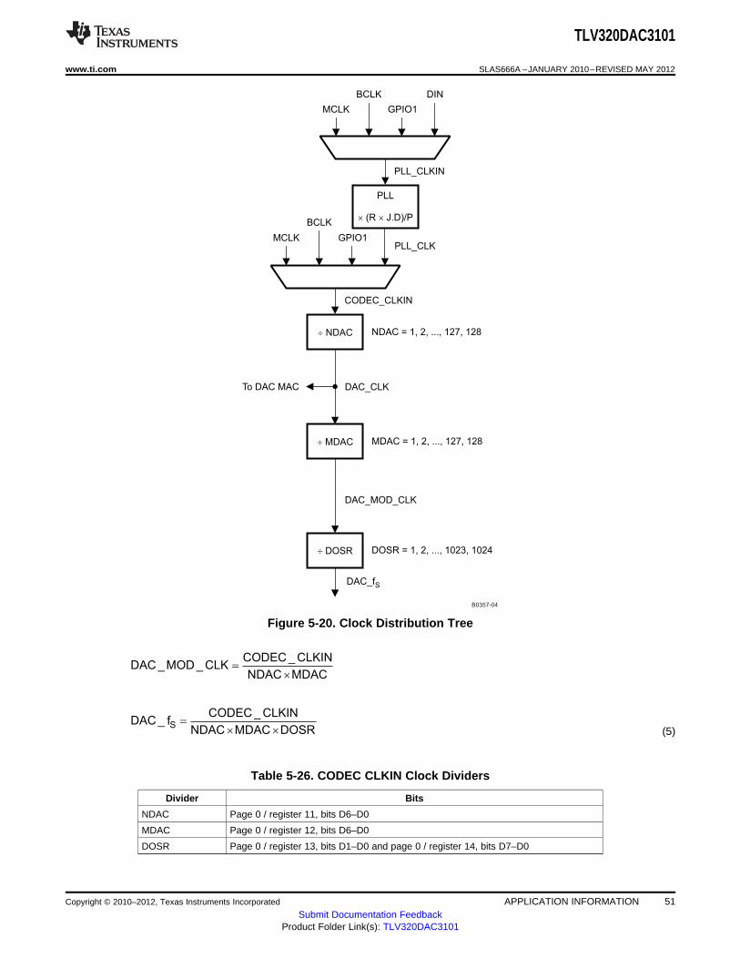
PLL
´ ´(R J.D)/P
PLL_CLKIN
CODEC_CLKIN
DAC_MOD_CLK
DAC_CLK
NDAC = 1, 2, ..., 127, 128
MDAC = 1, 2, ..., 127, 128
DOSR = 1, 2, ..., 1023, 1024
MCLK
BCLK
GPIO1
DIN
MCLK
BCLK
GPIO1PLL_CLK
¸ MDAC
¸ DOSR
¸ NDAC
To DAC MAC
DAC_fS
B0357-04
S
CODEC _ CLKINDAC _ f
NDAC MDAC DOSR=
´ ´
CODEC _ CLKINDAC _MOD _ CLK
NDAC MDAC=
´
TLV320DAC3101
www.ti.com SLAS666A –JANUARY 2010–REVISED MAY 2012
Figure 5-20. Clock Distribution Tree
(5)
Table 5-26. CODEC CLKIN Clock Dividers
Divider Bits
NDAC Page 0 / register 11, bits D6–D0
MDAC Page 0 / register 12, bits D6–D0
DOSR Page 0 / register 13, bits D1–D0 and page 0 / register 14, bits D7–D0
Copyright © 2010–2012, Texas Instruments Incorporated APPLICATION INFORMATION 51Submit Documentation Feedback
Product Folder Link(s): TLV320DAC3101
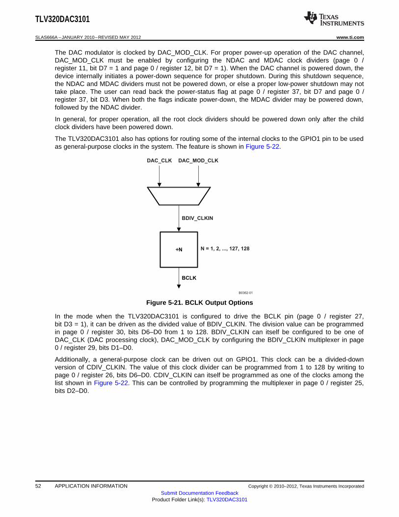
÷N
BCLK
DAC_CLK DAC_MOD_CLK
BDIV_CLKIN
N = 1, 2, ..., 127, 128
B0362-01
TLV320DAC3101
SLAS666A –JANUARY 2010–REVISED MAY 2012 www.ti.com
The DAC modulator is clocked by DAC_MOD_CLK. For proper power-up operation of the DAC channel,DAC_MOD_CLK must be enabled by configuring the NDAC and MDAC clock dividers (page 0 /register 11, bit D7 = 1 and page 0 / register 12, bit D7 = 1). When the DAC channel is powered down, thedevice internally initiates a power-down sequence for proper shutdown. During this shutdown sequence,the NDAC and MDAC dividers must not be powered down, or else a proper low-power shutdown may nottake place. The user can read back the power-status flag at page 0 / register 37, bit D7 and page 0 /register 37, bit D3. When both the flags indicate power-down, the MDAC divider may be powered down,followed by the NDAC divider.
In general, for proper operation, all the root clock dividers should be powered down only after the childclock dividers have been powered down.
The TLV320DAC3101 also has options for routing some of the internal clocks to the GPIO1 pin to be usedas general-purpose clocks in the system. The feature is shown in Figure 5-22.
Figure 5-21. BCLK Output Options
In the mode when the TLV320DAC3101 is configured to drive the BCLK pin (page 0 / register 27,bit D3 = 1), it can be driven as the divided value of BDIV_CLKIN. The division value can be programmedin page 0 / register 30, bits D6–D0 from 1 to 128. BDIV_CLKIN can itself be configured to be one ofDAC_CLK (DAC processing clock), DAC_MOD_CLK by configuring the BDIV_CLKIN multiplexer in page0 / register 29, bits D1–D0.
Additionally, a general-purpose clock can be driven out on GPIO1. This clock can be a divided-downversion of CDIV_CLKIN. The value of this clock divider can be programmed from 1 to 128 by writing topage 0 / register 26, bits D6–D0. CDIV_CLKIN can itself be programmed as one of the clocks among thelist shown in Figure 5-22. This can be controlled by programming the multiplexer in page 0 / register 25,bits D2–D0.
52 APPLICATION INFORMATION Copyright © 2010–2012, Texas Instruments Incorporated
Submit Documentation FeedbackProduct Folder Link(s): TLV320DAC3101
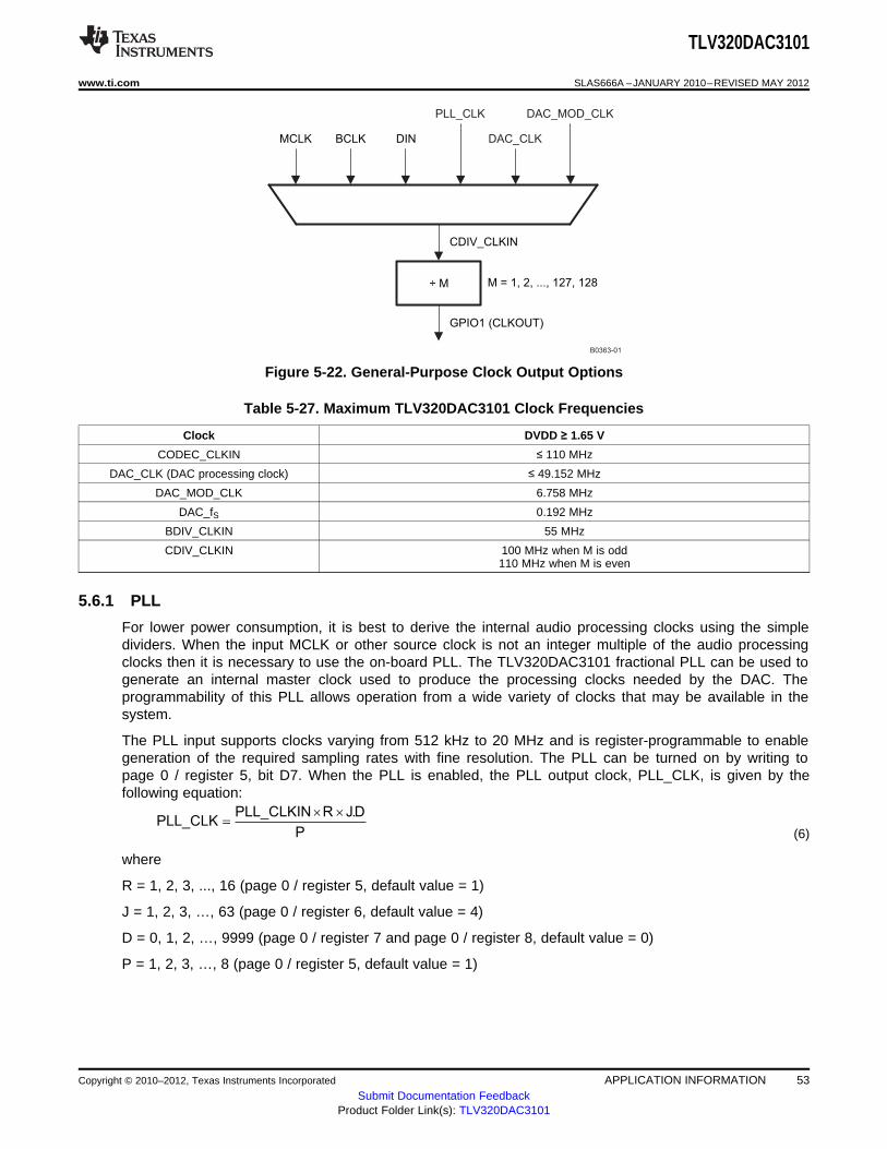
÷ M
GPIO1 (CLKOUT)
CDIV_CLKIN
MCLK BCLK DIN
PLL_CLK
DAC_CLK
DAC_MOD_CLK
M = 1, 2, ..., 127, 128
B0363-01
PLL_CLKIN R J.DPLL_CLK
P
´ ´
=
TLV320DAC3101
www.ti.com SLAS666A –JANUARY 2010–REVISED MAY 2012
Figure 5-22. General-Purpose Clock Output Options
Table 5-27. Maximum TLV320DAC3101 Clock Frequencies
Clock DVDD ≥ 1.65 V
CODEC_CLKIN ≤ 110 MHz
DAC_CLK (DAC processing clock) ≤ 49.152 MHz
DAC_MOD_CLK 6.758 MHz
DAC_fS 0.192 MHz
BDIV_CLKIN 55 MHz
CDIV_CLKIN 100 MHz when M is odd110 MHz when M is even
5.6.1 PLL
For lower power consumption, it is best to derive the internal audio processing clocks using the simpledividers. When the input MCLK or other source clock is not an integer multiple of the audio processingclocks then it is necessary to use the on-board PLL. The TLV320DAC3101 fractional PLL can be used togenerate an internal master clock used to produce the processing clocks needed by the DAC. Theprogrammability of this PLL allows operation from a wide variety of clocks that may be available in thesystem.
The PLL input supports clocks varying from 512 kHz to 20 MHz and is register-programmable to enablegeneration of the required sampling rates with fine resolution. The PLL can be turned on by writing topage 0 / register 5, bit D7. When the PLL is enabled, the PLL output clock, PLL_CLK, is given by thefollowing equation:
(6)
where
R = 1, 2, 3, ..., 16 (page 0 / register 5, default value = 1)
J = 1, 2, 3, …, 63 (page 0 / register 6, default value = 4)
D = 0, 1, 2, …, 9999 (page 0 / register 7 and page 0 / register 8, default value = 0)
P = 1, 2, 3, …, 8 (page 0 / register 5, default value = 1)
Copyright © 2010–2012, Texas Instruments Incorporated APPLICATION INFORMATION 53Submit Documentation Feedback
Product Folder Link(s): TLV320DAC3101
PLL _ CLKIN512 kHz 20 MHz
P£ £
PLL _ CLKIN10 MHz 20 MHz
P£ £
TLV320DAC3101
SLAS666A –JANUARY 2010–REVISED MAY 2012 www.ti.com
The PLL can be turned on via page 0 / register 5, bit D7. The variable P can be programmed via page 0 /register 5, bits D6–D4. The variable R can be programmed via page 0 / register 5, bits D3–D0. Thevariable J can be programmed via page 0 / register 6, bits D5–D0. The variable D is 14 bits and isprogrammed into two registers. The MSB portion can be programmed via page 0 / register 7, bits D5–D0,and the LSB portion is programmed via page 0 / register 8, bits D7–D0. For proper update of the D dividervalue, page 0 / register 7 must be programmed first, followed immediately by page 0 / register 8. Unlessthe write to page 0 / register 8 is completed, the new value of D does not take effect.
When the PLL is enabled, the following conditions must be satisfied:• When the PLL is enabled and D = 0, the following conditions must be satisfied for PLL_CLKIN:
80 MHz ≤ (PLL_CLKIN × J.D × R/P) ≤ 110 MHz
4 ≤ R × J ≤ 259(7)
• When the PLL is enabled and D ≠ 0, the following conditions must be satisfied for PLL_CLKIN:
80 MHz ≤ PLL_CLKIN × J.D × R/P ≤ 110 MHz
R = 1(8)
The PLL can be powered up independently from the DAC block, and can also be used as a general-purpose PLL by routing its output to the GPIO output. After powering up the PLL, PLL_CLK is availabletypically after 10 ms.
The clocks for the codec and various signal processing blocks, CODEC_CLKIN, can be generated fromthe MCLK input, BCLK input, GPIO input, or PLL_CLK (page 0 / register 4, bits D1–D0).
If CODEC_CLKIN is derived from the PLL, then the PLL must be powered up first and powered down last.
Table 5-28 lists several example cases of typical PLL_CLKIN rates and how to program the PLL toachieve a sample rate, fS, of either 44.1 kHz or 48 kHz.
Table 5-28. PLL Example Configurations
PLL_CLKIN (MHz) PLLP PLLR PLLJ PLLD MDAC NDAC DOSR
fS = 44.1 kHz
2.8224 1 3 10 0 3 5 128
5.6448 1 3 5 0 3 5 128
12 1 1 7 560 3 5 128
13 1 1 6 3504 6 3 104
16 1 1 5 2920 3 5 128
19.2 1 1 4 4100 3 5 128
48 4 1 7 560 3 5 128
fS = 48 kHz
2.048 1 3 14 0 7 2 128
3.072 1 4 7 0 7 2 128
4.096 1 3 7 0 7 2 128
6.144 1 2 7 0 7 2 128
8.192 1 4 3 0 4 4 128
12 1 1 7 1680 7 2 128
16 1 1 5 3760 7 2 128
19.2 1 1 4 4800 7 2 128
54 APPLICATION INFORMATION Copyright © 2010–2012, Texas Instruments Incorporated
Submit Documentation FeedbackProduct Folder Link(s): TLV320DAC3101
InternalOscillator ÷8 0
1
P3/R16, Bits D6-D0
MCLK
P3/R16, Bit D7
Interval timers
ProgrammableDivider
Powered on ifinternal oscillator is
selected
Used for de-bounce time forheadset detection logic,various power up timers andfor generation of interrupts
TLV320DAC3101
www.ti.com SLAS666A –JANUARY 2010–REVISED MAY 2012
Table 5-28. PLL Example Configurations (continued)
PLL_CLKIN (MHz) PLLP PLLR PLLJ PLLD MDAC NDAC DOSR
fS = 44.1 kHz
48 4 1 7 1680 7 2 128
5.6.2 Timer
The internal clock runs nominally at 8.2 MHz. This is used for various internal timing intervals, de-bouncelogics and interrupts. The MCLK divider must be set such a way that the divider output is ~1 MHz for thetimers to be closer to the programmed value.
Figure 5-23. Interval Timer Clock Selection
5.7 Digital Audio and Control Interface
5.7.1 Digital Audio Interface
Audio data is transferred between the host processor and the TLV320DAC3101 via the digital audio dataserial interface, or audio bus. The audio bus on this device is very flexible, including left- or right-justifieddata options, support for I2S or DSP protocols, programmable data length options, a TDM mode formultichannel operation, very flexible master/slave configurability for each bus-clock line, and the ability tocommunicate with multiple devices within a system directly.
The audio bus of the TLV320DAC3101 can be configured for left- or right-justified, I2S, DSP, or TDMmodes of operation, where communication with standard telephony interfaces is supported within the TDMmode. These modes are all MSB-first, with data width programmable as 16, 20, 24, or 32 bits byconfiguring page 0 / register 27, bits D5–D4. In addition, the word clock and bit clock can beindependently configured in either master or slave mode for flexible connectivity to a wide variety ofprocessors. The word clock is used to define the beginning of a frame, and may be programmed as eithera pulse or a square-wave signal. The frequency of this clock corresponds to the DAC sampling frequency.
The bit clock is used to clock in and clock out the digital audio data across the serial bus. When in mastermode, this signal can be programmed to generate variable clock pulses by controlling the bit-clock dividerin page 0 / register 30 (see Figure 5-20). The number of bit-clock pulses in a frame may need adjustmentto accommodate various word lengths as well as to support the case when multiple TLV320DAC3101smay share the same audio bus.
Copyright © 2010–2012, Texas Instruments Incorporated APPLICATION INFORMATION 55Submit Documentation Feedback
Product Folder Link(s): TLV320DAC3101
BCLK
WCLK
1 00 1 0
T0149-05
1/fS
LSBMSB
Left Channel Right Channel
2 2DIN n–1 n–1n–2 n–2n–3 n–3
TLV320DAC3101
SLAS666A –JANUARY 2010–REVISED MAY 2012 www.ti.com
The TLV320DAC3101 also includes a feature to offset the position of start of data transfer with respect tothe word clock. This offset can be controlled in terms of number of bit clocks and can be programmed inpage 0 / register 28.
The TLV320DAC3101 also has the feature of inverting the polarity of the bit clock used for transferring theaudio data as compared to the default clock polarity used. This feature can be used independently of themode of audio interface chosen. This can be configured via page 0 / register 29, bit D3.
By default, when the word clocks and bit clocks are generated by the TLV320DAC3101, these clocks areactive only when the DAC is powered up within the device. This is done to save power. However, it alsosupports a feature when both the word clocks and bit clocks can be active even when the codec in thedevice is powered down. This is useful when using the TDM mode with multiple codecs on the same bus,or when word clocks or bit clocks are used in the system as general-purpose clocks.
5.7.1.1 Right-Justified Mode
The audio interface of the TLV320DAC3101 can be put into the right-justified mode by programmingpage 0 / register 27, bits D7–D6 = 10. In right-justified mode, the LSB of the left channel is valid on therising edge of the bit clock preceding the falling edge of the word clock. Similarly, the LSB of the rightchannel is valid on the rising edge of the bit clock preceding the rising edge of the word clock.
Figure 5-24. Timing Diagram for Right-Justified Mode
For the right-justified mode, the number of bit clocks per frame should be greater than or equal to twicethe programmed word length of the data.
5.7.1.2 Left-Justified Mode
The audio interface of the TLV320DAC3101 can be put into left-justified mode by programming page 0 /register 27, bits D7–D6 = 11. In left-justified mode, the MSB of the right channel is valid on the rising edgeof the bit clock following the falling edge of the word clock. Similarly, the MSB of the left channel is validon the rising edge of the bit clock following the rising edge of the word clock.
56 APPLICATION INFORMATION Copyright © 2010–2012, Texas Instruments Incorporated
Submit Documentation FeedbackProduct Folder Link(s): TLV320DAC3101
LD(n) LD(n+1)
WORDCLOCK
BITCLOCK
DATA -1
-2
-3
2 1 03 -1
-2
-3
2 1 03 -1
-2
N N N N N N N N N-3
RD(n)
LEFT CHANNEL RIGHT CHANNEL
LD(n) = n'th sample of left channel data RD(n) = n'th sample of right channel data
LD(n) LD(n+1)
WORDCLOCK
BITCLOCK
DATA -1
-2
-3
2 1 03 -1
-2
-3
2 1 03 -1
-2
N N N N N N N N N-3
RD(n)
LEFT CHANNEL RIGHT CHANNEL
LD(n) = n'th sample of left channel data RD(n) = n'th sample of right channel data
LD(n) LD(n+1)
WORDCLOCK
BITCLOCK
DATA 3N-1
N-2
N-3
2 1 03N-1
N-2
N-3
2 1 03N-1
N-2
N-3
RD(n)
LEFT CHANNEL RIGHT CHANNEL
LD(n) = n'th sample of left channel data RD(n) = n'th sample of right channel data
TLV320DAC3101
www.ti.com SLAS666A –JANUARY 2010–REVISED MAY 2012
Figure 5-25. Timing Diagram for Left-Justified Mode
Figure 5-26. Timing Diagram for Left-Justified Mode With Offset = 1
Figure 5-27. Timing Diagram for Left-Justified Mode With Offset = 0 and Inverted Bit Clock
For the left-justified mode, the number of bit clocks per frame should be greater than or equal to twice theprogrammed word length of the data. Also, the programmed offset value should be less than the numberof bit clocks per frame by at least the programmed word length of the data.
5.7.1.3 I2S Mode
The audio interface of the TLV320DAC3101 can be put into I2S mode by programming page 0 /register 27, bits D7–D6 = 00. In I2S mode, the MSB of the left channel is valid on the second rising edgeof the bit clock after the falling edge of the word clock. Similarly, the MSB of the right channel is valid onthe second rising edge of the bit clock after the rising edge of the word clock.
Copyright © 2010–2012, Texas Instruments Incorporated APPLICATION INFORMATION 57Submit Documentation Feedback
Product Folder Link(s): TLV320DAC3101
LD(n) LD(n+1)
WORDCLOCK
BITCLOCK
DATA -1
-2
-3
2 1 03 -1
-2
-3
2 1 03 -1
-2
N N N N N N N N N-3
3
RD(n)
LEFT CHANNEL RIGHT CHANNEL
LD(n) = n'th sample of left channel data RD(n) = n'th sample of right channel data
LD(n) LD (n+1)
WORDCLOCK
BITCLOCK
DATA -1
4 3 25 1 0 -1
4 3 25 1 0N N N
-1
5
RD(n)
LEFT CHANNEL RIGHT CHANNEL
LD(n) = n'th sample of left channel data RD(n) = n'th sample of right channel data
LD(n) LD(n+1)
WORDCLOCK
BITCLOCK
DATA -1
-2
-3
2 1 03 -1
-2
-3
2 1 03 -1
-2
N N N N N N N N N-3
3
RD(n)
LEFT CHANNEL RIGHT CHANNEL
LD(n) = n'th sample of left channel data RD(n) = n'th sample of right channel data
TLV320DAC3101
SLAS666A –JANUARY 2010–REVISED MAY 2012 www.ti.com
Figure 5-28. Timing Diagram for I2S Mode
Figure 5-29. Timing Diagram for I2S Mode With Offset = 2
Figure 5-30. Timing Diagram for I2S Mode With Offset = 0 and Bit Clock Inverted
For I2S mode, the number of bit clocks per channel should be greater than or equal to the programmedword length of the data. Also, the programmed offset value should be less than the number of bit clocksper frame by at least the programmed word length of the data.
5.7.1.4 DSP Mode
The audio interface of the TLV320DAC3101 can be put into DSP mode by programming page 0 /register 27, bits D7–D6 = 01. In DSP mode, the falling edge of the word clock starts the data transfer withthe left-channel data first and immediately followed by the right-channel data. Each data bit is valid on thefalling edge of the bit clock.
58 APPLICATION INFORMATION Copyright © 2010–2012, Texas Instruments Incorporated
Submit Documentation FeedbackProduct Folder Link(s): TLV320DAC3101
LD(n) LD(n+1)
BITCLOCK
DATA -1
-2
-3
2 1 03 -1
-2
-3
03 2 1 -1
-2
N N N N N N N N N-3
3
RD(n)
WORDCLOCK
LEFT CHANNEL RIGHT CHANNEL
LD(n) = n'th sample of left channel data RD(n) = n'th sample of right channel data
LD(n) LD(n+1)
BITCLOCK
DATA -1
-2
-3
2 1 03 -1
-2
-3
03 2 1 -1
-2
N N N N N N N N N-3
RD(n)
WORDCLOCK
LEFT CHANNEL RIGHT CHANNEL
LD(n) = n'th sample of left channel data RD(n) = n'th sample of right channel data
LD(n) LD(n+1)
BIT
CLOCK
DATAN-
1
N-
2
N-
3
2 1 03N-
1
N-
2
N-
3
03 2 1N-
1
N-
2
N-
3
3
RD(n)
WORD
CLOCKLEFT CHANNEL RIGHT CHANNEL
TLV320DAC3101
www.ti.com SLAS666A –JANUARY 2010–REVISED MAY 2012
Figure 5-31. Timing Diagram for DSP Mode
Figure 5-32. Timing Diagram for DSP Mode With Offset = 1
Figure 5-33. Timing Diagram for DSP Mode With Offset = 0 and Bit Clock Inverted
For the DSP mode, the number of bit clocks per frame should be greater than or equal to twice theprogrammed word length of the data. Also, the programmed offset value should be less than the numberof bit clocks per frame by at least the programmed word length of the data.
5.7.2 Primary and Secondary Digital Audio Interface Selection
The audio serial interface on the TLV320DAC3101 has extensive I/O control to allow communication withtwo independent processors for audio data. The processors can communicate with the device one at atime. This feature is enabled by register programming of the various pin selections. Table 5-29 shows theprimary and secondary audio interface selection and registers. Figure 5-34 is a high-level diagramshowing the general signal flow and multiplexing for the primary and secondary audio interfaces.
Table 5-29. Primary and Secondary Audio Interface Selection
Desired Pin Possible Page 0 Registers CommentFunction Pins
R27/D2 = 1 Primary WCLK is output from codecPrimary WCLK WCLK(OUT) R33/D5–D4 Select source of primary WCLK (DAC_fS or secondary WCLK)
Copyright © 2010–2012, Texas Instruments Incorporated APPLICATION INFORMATION 59Submit Documentation Feedback
Product Folder Link(s): TLV320DAC3101
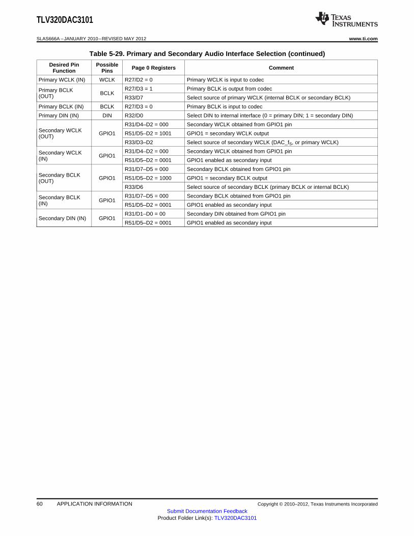
TLV320DAC3101
SLAS666A –JANUARY 2010–REVISED MAY 2012 www.ti.com
Table 5-29. Primary and Secondary Audio Interface Selection (continued)
Desired Pin Possible Page 0 Registers CommentFunction Pins
Primary WCLK (IN) WCLK R27/D2 = 0 Primary WCLK is input to codec
R27/D3 = 1 Primary BCLK is output from codecPrimary BCLK BCLK(OUT) R33/D7 Select source of primary WCLK (internal BCLK or secondary BCLK)
Primary BCLK (IN) BCLK R27/D3 = 0 Primary BCLK is input to codec
Primary DIN (IN) DIN R32/D0 Select DIN to internal interface (0 = primary DIN; 1 = secondary DIN)
R31/D4–D2 = 000 Secondary WCLK obtained from GPIO1 pinSecondary WCLK GPIO1 R51/D5–D2 = 1001 GPIO1 = secondary WCLK output(OUT)
R33/D3–D2 Select source of secondary WCLK (DAC_fS, or primary WCLK)
R31/D4–D2 = 000 Secondary WCLK obtained from GPIO1 pinSecondary WCLK GPIO1(IN) R51/D5–D2 = 0001 GPIO1 enabled as secondary input
R31/D7–D5 = 000 Secondary BCLK obtained from GPIO1 pinSecondary BCLK GPIO1 R51/D5–D2 = 1000 GPIO1 = secondary BCLK output(OUT)
R33/D6 Select source of secondary BCLK (primary BCLK or internal BCLK)
R31/D7–D5 = 000 Secondary BCLK obtained from GPIO1 pinSecondary BCLK GPIO1(IN) R51/D5–D2 = 0001 GPIO1 enabled as secondary input
R31/D1–D0 = 00 Secondary DIN obtained from GPIO1 pinSecondary DIN (IN) GPIO1
R51/D5–D2 = 0001 GPIO1 enabled as secondary input
60 APPLICATION INFORMATION Copyright © 2010–2012, Texas Instruments Incorporated
Submit Documentation FeedbackProduct Folder Link(s): TLV320DAC3101
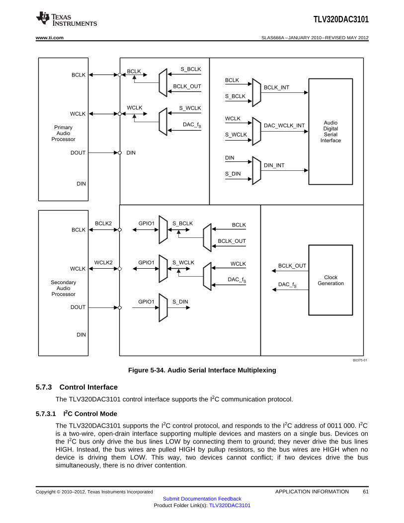
BCLK_OUT
DAC_fS
ClockGeneration
BCLK
S_BCLK
WCLK
S_WCLK
DIN
S_DIN
AudioDigitalSerial
Interface
BCLK_INT
DAC_WCLK_INT
DIN_INT
BCLK
WCLK
BCLK
DIN
WCLK
DIN
DOUT
PrimaryAudio
Processor
S_WCLK
S_BCLK
BCLK_OUT
GPIO1
GPIO1
S_BCLK BCLK
BCLK_OUT
S_WCLK WCLK
DAC_fS
DAC_fS
GPIO1 S_DIN
WCLK
DIN
DOUT
SecondaryAudio
Processor
BCLK
BCLK2
WCLK2
B0375-01
TLV320DAC3101
www.ti.com SLAS666A –JANUARY 2010–REVISED MAY 2012
Figure 5-34. Audio Serial Interface Multiplexing
5.7.3 Control Interface
The TLV320DAC3101 control interface supports the I2C communication protocol.
5.7.3.1 I2C Control Mode
The TLV320DAC3101 supports the I2C control protocol, and responds to the I2C address of 0011 000. I2Cis a two-wire, open-drain interface supporting multiple devices and masters on a single bus. Devices onthe I2C bus only drive the bus lines LOW by connecting them to ground; they never drive the bus linesHIGH. Instead, the bus wires are pulled HIGH by pullup resistors, so the bus wires are HIGH when nodevice is driving them LOW. This way, two devices cannot conflict; if two devices drive the bussimultaneously, there is no driver contention.
Copyright © 2010–2012, Texas Instruments Incorporated APPLICATION INFORMATION 61Submit Documentation Feedback
Product Folder Link(s): TLV320DAC3101
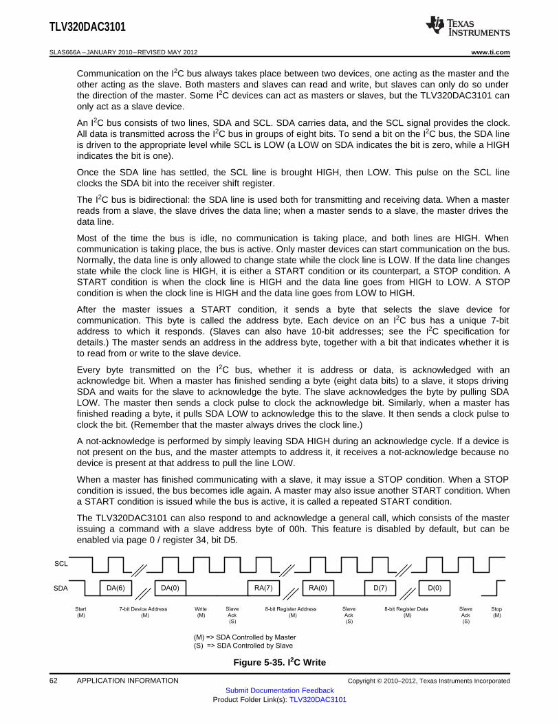
DA(6) DA(0) RA(7) RA(0) D(7) D(0)
Start
(M)
7-bit Device Address
(M)
Write
(M)
Slave
Ack
(S)
8-bit Register Address
(M)
Slave
Ack
(S)
8-bit Register Data
(M)
Stop
(M)
Slave
Ack
(S)
SDA
SCL
(M) => SDA Controlled by Master
(S) => SDA Controlled by Slave
TLV320DAC3101
SLAS666A –JANUARY 2010–REVISED MAY 2012 www.ti.com
Communication on the I2C bus always takes place between two devices, one acting as the master and theother acting as the slave. Both masters and slaves can read and write, but slaves can only do so underthe direction of the master. Some I2C devices can act as masters or slaves, but the TLV320DAC3101 canonly act as a slave device.
An I2C bus consists of two lines, SDA and SCL. SDA carries data, and the SCL signal provides the clock.All data is transmitted across the I2C bus in groups of eight bits. To send a bit on the I2C bus, the SDA lineis driven to the appropriate level while SCL is LOW (a LOW on SDA indicates the bit is zero, while a HIGHindicates the bit is one).
Once the SDA line has settled, the SCL line is brought HIGH, then LOW. This pulse on the SCL lineclocks the SDA bit into the receiver shift register.
The I2C bus is bidirectional: the SDA line is used both for transmitting and receiving data. When a masterreads from a slave, the slave drives the data line; when a master sends to a slave, the master drives thedata line.
Most of the time the bus is idle, no communication is taking place, and both lines are HIGH. Whencommunication is taking place, the bus is active. Only master devices can start communication on the bus.Normally, the data line is only allowed to change state while the clock line is LOW. If the data line changesstate while the clock line is HIGH, it is either a START condition or its counterpart, a STOP condition. ASTART condition is when the clock line is HIGH and the data line goes from HIGH to LOW. A STOPcondition is when the clock line is HIGH and the data line goes from LOW to HIGH.
After the master issues a START condition, it sends a byte that selects the slave device forcommunication. This byte is called the address byte. Each device on an I2C bus has a unique 7-bitaddress to which it responds. (Slaves can also have 10-bit addresses; see the I2C specification fordetails.) The master sends an address in the address byte, together with a bit that indicates whether it isto read from or write to the slave device.
Every byte transmitted on the I2C bus, whether it is address or data, is acknowledged with anacknowledge bit. When a master has finished sending a byte (eight data bits) to a slave, it stops drivingSDA and waits for the slave to acknowledge the byte. The slave acknowledges the byte by pulling SDALOW. The master then sends a clock pulse to clock the acknowledge bit. Similarly, when a master hasfinished reading a byte, it pulls SDA LOW to acknowledge this to the slave. It then sends a clock pulse toclock the bit. (Remember that the master always drives the clock line.)
A not-acknowledge is performed by simply leaving SDA HIGH during an acknowledge cycle. If a device isnot present on the bus, and the master attempts to address it, it receives a not-acknowledge because nodevice is present at that address to pull the line LOW.
When a master has finished communicating with a slave, it may issue a STOP condition. When a STOPcondition is issued, the bus becomes idle again. A master may also issue another START condition. Whena START condition is issued while the bus is active, it is called a repeated START condition.
The TLV320DAC3101 can also respond to and acknowledge a general call, which consists of the masterissuing a command with a slave address byte of 00h. This feature is disabled by default, but can beenabled via page 0 / register 34, bit D5.
Figure 5-35. I2C Write
62 APPLICATION INFORMATION Copyright © 2010–2012, Texas Instruments Incorporated
Submit Documentation FeedbackProduct Folder Link(s): TLV320DAC3101
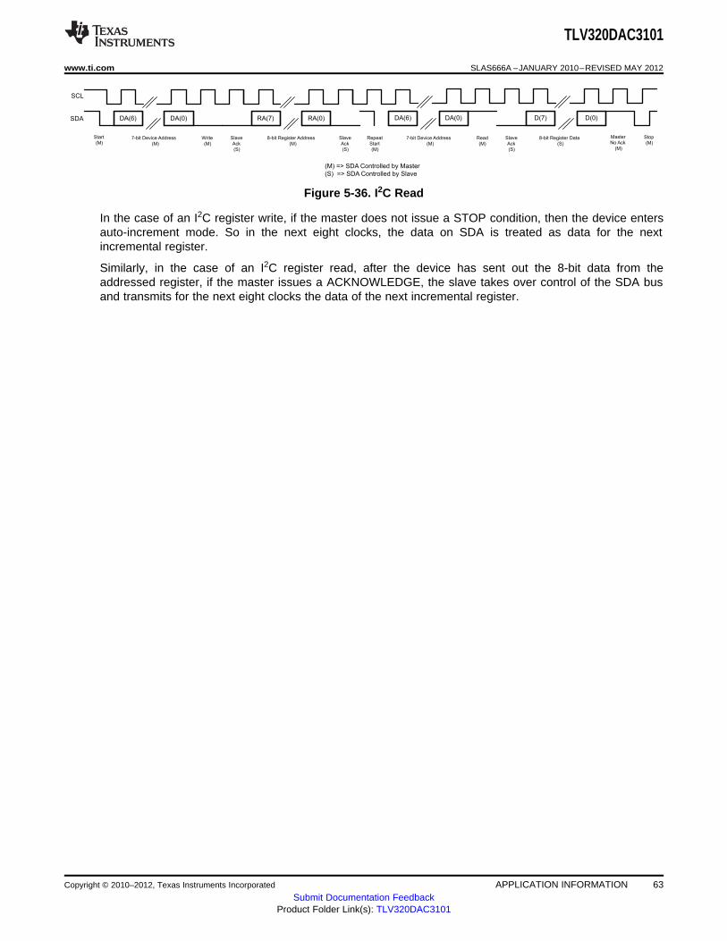
Start
(M)7-bit Device Address
(M)
Write
(M)
Slave
Ack
(S)
8-bit Register Address
(M)
Slave
Ack
(S)
SDA
SCL
7-bit Device Address
(M)
Read
(M)
Slave
Ack
(S)
DA(6) DA(0) RA(7) RA(0) DA(6) DA(0) D(7) D(0)
8-bit Register Data
(S)
Stop
(M)
Master
No Ack
(M)
Repeat
Start
(M)
(M) => SDA Controlled by Master
(S) => SDA Controlled by Slave
TLV320DAC3101
www.ti.com SLAS666A –JANUARY 2010–REVISED MAY 2012
Figure 5-36. I2C Read
In the case of an I2C register write, if the master does not issue a STOP condition, then the device entersauto-increment mode. So in the next eight clocks, the data on SDA is treated as data for the nextincremental register.
Similarly, in the case of an I2C register read, after the device has sent out the 8-bit data from theaddressed register, if the master issues a ACKNOWLEDGE, the slave takes over control of the SDA busand transmits for the next eight clocks the data of the next incremental register.
Copyright © 2010–2012, Texas Instruments Incorporated APPLICATION INFORMATION 63Submit Documentation Feedback
Product Folder Link(s): TLV320DAC3101
TLV320DAC3101
SLAS666A –JANUARY 2010–REVISED MAY 2012 www.ti.com
6 REGISTER MAP
6.1 TLV320DAC3101 Register Map
All features on this device are addressed using the I2C bus. All of the writable registers can be read back.However, some registers contain status information or data, and are available for reading only.
The TLV320DAC3101 contains several pages of 8-bit registers, and each page can contain up to 128registers. The register pages are divided up based on functional blocks for this device. The pages definedfor the TLV320DAC3101 are 0, 1, 3, 8–9, 12–13 (DAC coefficient pages). Page 0 is the default homepage after RESET. Page control is done by writing a new page value into register 0 of the current page.
The control registers for the TLV320DAC3101 are described in detail as follows. All registers are 8 bits inwidth, with D7 referring to the most-significant bit of each register, and D0 referring to the least-significantbit.
Pages 0, 1, 3, 8–9, and 12–13 are available for use; however, all other pages and registers are reserved.Do not read from or write to reserved pages and registers. Also, do not write other than the reset valuesfor the reserved bits and read-only bits of non-reserved registers; otherwise, device functionality failurecan occur.
Note that the page and register numbers are shown in decimal format. For use in microcode thesedecimal values may need to be converted to hexadecimal format. For convienience the registernumbers are shown in both formats whereas the page numbers are shown only in decimal format.
Table 6-1. Summary of Register Map
Page Number Description
0 Page 0 is the default page on power up. Configuration for serial interface, digital I/O, etc.
1 Configuration for DAC, output drivers, volume controls, etc.
Register 16 controls the MCLK divider that controls the interrupt pulse duration, debounce timing, and detection-block3 clock.
8–9 DAC filter and DRC coefficients (buffer A)
12–13 DAC filter and DRC coefficients (buffer B)
6.2 Control Registers, Page 0 (Default Page): Clock Multipliers, Dividers, SerialInterfaces, Flags, Interrupts, and GPIOs
Page 0 / Register 0 (0x00): Page Control RegisterREAD/ RESETBIT DESCRIPTIONWRITE VALUE
D7–D0 R/W 0000 0000 0000 0000: Page 0 selected0000 0001: Page 1 selected...1111 1110: Page 254 selected1111 1111: Page 255 selected
Page 0 / Register 1 (0x01): Software ResetREAD/ RESETBIT DESCRIPTIONWRITE VALUE
D7–D1 R/W 0000 000 Reserved. Write only zeros to these bits.
D0 R/W 0 0: Don't care1: Self-clearing software reset for control register
Page 0 / Register 2 (0x02): ReservedREAD/ RESETBIT DESCRIPTIONWRITE VALUE
D7–D0 R XXXX XXXX Reserved. Do not write to this register.
64 REGISTER MAP Copyright © 2010–2012, Texas Instruments Incorporated
Submit Documentation FeedbackProduct Folder Link(s): TLV320DAC3101
TLV320DAC3101
www.ti.com SLAS666A –JANUARY 2010–REVISED MAY 2012
Page 0 / Register 3 (0x03): OT FLAGREAD/ RESETBIT DESCRIPTIONWRITE VALUE
D7–D2 R XXXX XX Reserved. Do not write to these bits.
D1 R 1 0: Overtemperature protection flag (active-low). Valid only if speaker amplifier is powered up1: Normal operation
D0 R/W X Reserved. Do not write to these bits.
Page 0 / Register 4 (0x04): Clock-Gen Muxing (1)
READ/ RESETBIT DESCRIPTIONWRITE VALUE
D7–D4 R/W 0000 Reserved. Write only zeros to these bits.
D3–D2 R/W 00 00: PLL_CLKIN = MCLK (device pin)01: PLL_CLKIN = BCLK (device pin)10: PLL_CLKIN = GPIO1 (device pin)11: PLL_CLKIN = DIN (can be used for the system where DAC is not used)
D1–D0 R/W 00 00: CODEC_CLKIN = MCLK (device pin)01: CODEC_CLKIN = BCLK (device pin)10: CODEC_CLKIN = GPIO1 (device pin)11: CODEC_CLKIN = PLL_CLK (generated on-chip)
(1) See Section 5.6 for more details on clock generation mutiplexing and dividers.
Page 0 / Register 5 (0x05): PLL P and R ValuesREAD/ RESETBIT DESCRIPTIONWRITE VALUE
D7 R/W 0 0: PLL is powered down.1: PLL is powered up.
D6–D4 R/W 001 000: PLL divider P = 8001: PLL divider P = 1010: PLL divider P = 2...110: PLL divider P = 6111: PLL divider P = 7
D3–D0 R/W 0001 0000: PLL multiplier R = 160001: PLL multiplier R = 10010: PLL multiplier R = 2...1110: PLL multiplier R = 141111: PLL multiplier R = 15
Page 0 / Register 6 (0x06): PLL J ValueREAD/ RESETBIT DESCRIPTIONWRITE VALUE
D7–D6 R/W 00 Reserved. Write only zeros to these bits.
D5–D0 R/W 00 0100 00 0000: Do not use (reserved)00 0001: PLL multiplier J = 100 0010: PLL multiplier J = 2...11 1110: PLL multiplier J = 6211 1111: PLL multiplier J = 63
Page 0 / Register 7 (0x07): PLL D-Value MSB (1)
READ/ RESETBIT DESCRIPTIONWRITE VALUE
D7–D6 R/W 00 Reserved. Write only zeros to these bits.
D5–D0 R/W 00 0000 PLL fractional multiplier D-value MSBs D[13:8]
(1) Note that this register is updated only when page 0 / register 8 is written immediately after page 0 / register 7.
Copyright © 2010–2012, Texas Instruments Incorporated REGISTER MAP 65Submit Documentation Feedback
Product Folder Link(s): TLV320DAC3101
TLV320DAC3101
SLAS666A –JANUARY 2010–REVISED MAY 2012 www.ti.com
Page 0 / Register 8 (0x08): PLL D-Value LSB (1)
READ/ RESETBIT DESCRIPTIONWRITE VALUE
D7–D0 R/W 0000 0000 PLL fractional multiplier D-value LSBs D[7:0]
(1) Note that page 0 / register 8 must be written immediately after page 0 / register 7.
Page 0 / Register 9 and Page 0 / Register 10: ReservedREAD/ RESETBIT DESCRIPTIONWRITE VALUE
D7–D0 R/W XXXX XXXX Reserved. Write only zeros to these bits.
Page 0 / Register 11 (0x0B): DAC NDAC_VALREAD/ RESETBIT DESCRIPTIONWRITE VALUE
D7 R/W 0 0: DAC NDAC divider is powered down.1: DAC NDAC divider is powered up.
D6–D0 R/W 000 0001 000 0000: DAC NDAC divider = 128000 0001: DAC NDAC divider = 1000 0010: DAC NDAC divider = 2...111 1110: DAC NDAC divider = 126111 1111: DAC NDAC divider = 127
Page 0 / Register 12 (0x0C): DAC MDAC_VALREAD/ RESETBIT DESCRIPTIONWRITE VALUE
D7 R/W 0 0: DAC MDAC divider is powered down.1: DAC MDAC divider is powered up.
D6–D0 R/W 000 0001 000 0000: DAC MDAC divider = 128000 0001: DAC MDAC divider = 1000 0010: DAC MDAC divider = 2...111 1110: DAC MDAC divider = 126111 1111: DAC MDAC divider = 127
Page 0 / Register 13 (0x0D): DAC DOSR_VAL MSBREAD/ RESETBIT DESCRIPTIONWRITE VALUE
D7–D2 R/W 0000 00 Reserved
D1–D0 R/W 00 DAC OSR value DOSR(9:8)
Page 0 / Register 14 (0x0E): DAC DOSR_VAL LSB (1) (2)
READ/ RESETBIT DESCRIPTIONWRITE VALUE
D7–D0 R/W 1000 0000 DAC OSR Value DOSR(7:0)0000 0000: DAC OSR(7:0) = 1024 (MSB page 0 / register 13, bits D1–D0 = 00)0000 0001: Reserved.0000 0010: DAC OSR(7:0) = 2 (MSB page 0 / register 13, bits D1–D0 = 00)...1111 1110: DAC OSR(7:0) = 1022 (MSB page 0 / register 13, bits D1–D0 = 11)1111 1111: DAC OSR(7:0) = Reserved. Do not use.
(1) DOSR must be a multiple of 2 when using filter type A, a multiple of 4 when using filter type B, and a multiple of 8 when using filter typeC.
(2) Note that page 0 / register 14 must be written to immediately after writing to page 0 / register 13.
Page 0 / Register 15–24: ReservedREAD/ RESETBIT DESCRIPTIONWRITE VALUE
D7–D0 R/W XXXX XXXX Reserved. Do not write to these registers.
66 REGISTER MAP Copyright © 2010–2012, Texas Instruments Incorporated
Submit Documentation FeedbackProduct Folder Link(s): TLV320DAC3101
TLV320DAC3101
www.ti.com SLAS666A –JANUARY 2010–REVISED MAY 2012
Page 0 / Register 25 (0x19): CLKOUT MUXREAD/ RESETBIT DESCRIPTIONWRITE VALUE
D7–D3 R/W 0000 0 Reserved
D2–D0 R/W 000 000: CDIV_CLKIN = MCLK (device pin)001: CDIV_CLKIN = BCLK (device pin)010: CDIV_CLKIN = DIN (can be used for the systems where DAC is not required)011: CDIV_CLKIN = PLL_CLK (generated on-chip)100: CDIV_CLKIN = DAC_CLK (generated on-chip)101: CDIV_CLKIN = DAC_MOD_CLK (generated on-chip)110: Reserved111: Reserved
Page 0 / Register 26 (0x1A): CLKOUT M_VALREAD/ RESETBIT DESCRIPTIONWRITE VALUE
D7 R/W 0 0: CLKOUT M divider is powered down.1: CLKOUT M divider is powered up.
D6–D0 R/W 000 0001 000 0000: CLKOUT divider M = 128000 0001: CLKOUT divider M = 1000 0010: CLKOUT divider M = 2...111 1110: CLKOUT divider M = 126111 1111: CLKOUT divider M = 127
Page 0 / Register 27 (0x1B): Codec Interface Control 1READ/ RESETBIT DESCRIPTIONWRITE VALUE
D7–D6 R/W 00 00: Codec interface = I2S01: Codec Interface = DSP10: Codec interface = RJF11: Codec interface = LJF
D5–D4 R/W 00 00: Codec interface word length = 16 bits01: Codec interface word length = 20 bits10: Codec interface word length = 24 bits11: Codec interface word length = 32 bits
D3 R/W 0 0: BCLK is input.1: BCLK is output.
D2 R/W 0 0: WCLK is input.1: WCLK is output.
D1–D0 R/W 00 Reserved
Page 0 / Register 28 (0x1C): Data-Slot Offset ProgrammabilityREAD/ RESETBIT DESCRIPTIONWRITE VALUE
D7–D0 R/W 0000 0000 Offset (Measured With Respect to WCLK Rising Edge in DSP Mode)0000 0000: Offset = 0 BCLKs0000 0001: Offset = 1 BCLK0000 0010: Offset = 2 BCLKs...1111 1110: Offset = 254 BCLKs1111 1111: Offset = 255 BCLKs
Copyright © 2010–2012, Texas Instruments Incorporated REGISTER MAP 67Submit Documentation Feedback
Product Folder Link(s): TLV320DAC3101
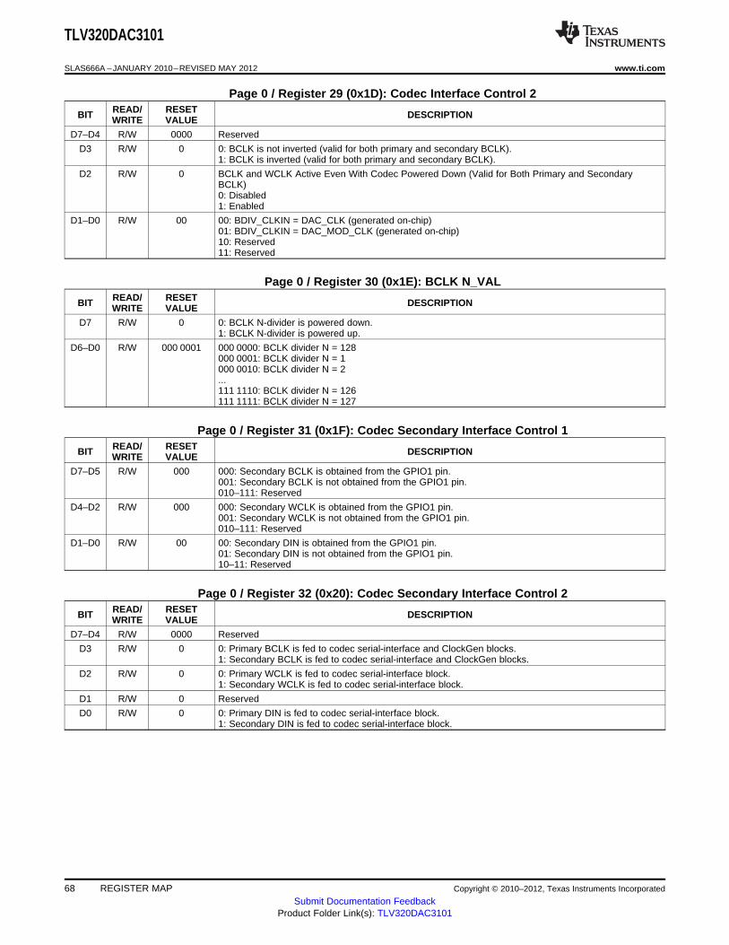
TLV320DAC3101
SLAS666A –JANUARY 2010–REVISED MAY 2012 www.ti.com
Page 0 / Register 29 (0x1D): Codec Interface Control 2READ/ RESETBIT DESCRIPTIONWRITE VALUE
D7–D4 R/W 0000 Reserved
D3 R/W 0 0: BCLK is not inverted (valid for both primary and secondary BCLK).1: BCLK is inverted (valid for both primary and secondary BCLK).
D2 R/W 0 BCLK and WCLK Active Even With Codec Powered Down (Valid for Both Primary and SecondaryBCLK)0: Disabled1: Enabled
D1–D0 R/W 00 00: BDIV_CLKIN = DAC_CLK (generated on-chip)01: BDIV_CLKIN = DAC_MOD_CLK (generated on-chip)10: Reserved11: Reserved
Page 0 / Register 30 (0x1E): BCLK N_VALREAD/ RESETBIT DESCRIPTIONWRITE VALUE
D7 R/W 0 0: BCLK N-divider is powered down.1: BCLK N-divider is powered up.
D6–D0 R/W 000 0001 000 0000: BCLK divider N = 128000 0001: BCLK divider N = 1000 0010: BCLK divider N = 2...111 1110: BCLK divider N = 126111 1111: BCLK divider N = 127
Page 0 / Register 31 (0x1F): Codec Secondary Interface Control 1READ/ RESETBIT DESCRIPTIONWRITE VALUE
D7–D5 R/W 000 000: Secondary BCLK is obtained from the GPIO1 pin.001: Secondary BCLK is not obtained from the GPIO1 pin.010–111: Reserved
D4–D2 R/W 000 000: Secondary WCLK is obtained from the GPIO1 pin.001: Secondary WCLK is not obtained from the GPIO1 pin.010–111: Reserved
D1–D0 R/W 00 00: Secondary DIN is obtained from the GPIO1 pin.01: Secondary DIN is not obtained from the GPIO1 pin.10–11: Reserved
Page 0 / Register 32 (0x20): Codec Secondary Interface Control 2READ/ RESETBIT DESCRIPTIONWRITE VALUE
D7–D4 R/W 0000 Reserved
D3 R/W 0 0: Primary BCLK is fed to codec serial-interface and ClockGen blocks.1: Secondary BCLK is fed to codec serial-interface and ClockGen blocks.
D2 R/W 0 0: Primary WCLK is fed to codec serial-interface block.1: Secondary WCLK is fed to codec serial-interface block.
D1 R/W 0 Reserved
D0 R/W 0 0: Primary DIN is fed to codec serial-interface block.1: Secondary DIN is fed to codec serial-interface block.
68 REGISTER MAP Copyright © 2010–2012, Texas Instruments Incorporated
Submit Documentation FeedbackProduct Folder Link(s): TLV320DAC3101
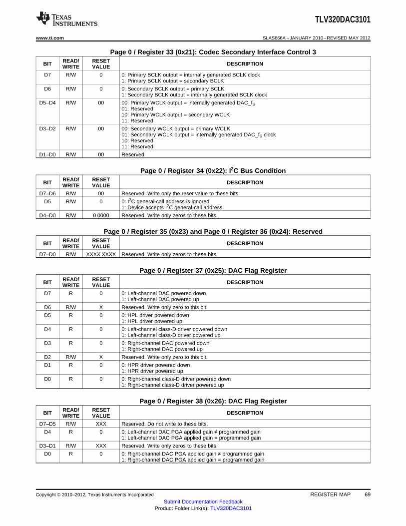
TLV320DAC3101
www.ti.com SLAS666A –JANUARY 2010–REVISED MAY 2012
Page 0 / Register 33 (0x21): Codec Secondary Interface Control 3READ/ RESETBIT DESCRIPTIONWRITE VALUE
D7 R/W 0 0: Primary BCLK output = internally generated BCLK clock1: Primary BCLK output = secondary BCLK
D6 R/W 0 0: Secondary BCLK output = primary BCLK1: Secondary BCLK output = internally generated BCLK clock
D5–D4 R/W 00 00: Primary WCLK output = internally generated DAC_fS01: Reserved10: Primary WCLK output = secondary WCLK11: Reserved
D3–D2 R/W 00 00: Secondary WCLK output = primary WCLK01: Secondary WCLK output = internally generated DAC_fS clock10: Reserved11: Reserved
D1–D0 R/W 00 Reserved
Page 0 / Register 34 (0x22): I2C Bus ConditionREAD/ RESETBIT DESCRIPTIONWRITE VALUE
D7–D6 R/W 00 Reserved. Write only the reset value to these bits.
D5 R/W 0 0: I2C general-call address is ignored.1: Device accepts I2C general-call address.
D4–D0 R/W 0 0000 Reserved. Write only zeros to these bits.
Page 0 / Register 35 (0x23) and Page 0 / Register 36 (0x24): ReservedREAD/ RESETBIT DESCRIPTIONWRITE VALUE
D7–D0 R/W XXXX XXXX Reserved. Write only zeros to these bits.
Page 0 / Register 37 (0x25): DAC Flag RegisterREAD/ RESETBIT DESCRIPTIONWRITE VALUE
D7 R 0 0: Left-channel DAC powered down1: Left-channel DAC powered up
D6 R/W X Reserved. Write only zero to this bit.
D5 R 0 0: HPL driver powered down1: HPL driver powered up
D4 R 0 0: Left-channel class-D driver powered down1: Left-channel class-D driver powered up
D3 R 0 0: Right-channel DAC powered down1: Right-channel DAC powered up
D2 R/W X Reserved. Write only zero to this bit.
D1 R 0 0: HPR driver powered down1: HPR driver powered up
D0 R 0 0: Right-channel class-D driver powered down1: Right-channel class-D driver powered up
Page 0 / Register 38 (0x26): DAC Flag RegisterREAD/ RESETBIT DESCRIPTIONWRITE VALUE
D7–D5 R/W XXX Reserved. Do not write to these bits.
D4 R 0 0: Left-channel DAC PGA applied gain ≠ programmed gain1: Left-channel DAC PGA applied gain = programmed gain
D3–D1 R/W XXX Reserved. Write only zeros to these bits.
D0 R 0 0: Right-channel DAC PGA applied gain ≠ programmed gain1: Right-channel DAC PGA applied gain = programmed gain
Copyright © 2010–2012, Texas Instruments Incorporated REGISTER MAP 69Submit Documentation Feedback
Product Folder Link(s): TLV320DAC3101
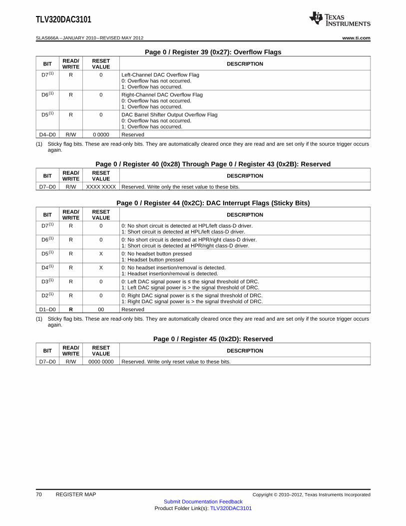
TLV320DAC3101
SLAS666A –JANUARY 2010–REVISED MAY 2012 www.ti.com
Page 0 / Register 39 (0x27): Overflow FlagsREAD/ RESETBIT DESCRIPTIONWRITE VALUE
D7 (1) R 0 Left-Channel DAC Overflow Flag0: Overflow has not occurred.1: Overflow has occurred.
D6 (1) R 0 Right-Channel DAC Overflow Flag0: Overflow has not occurred.1: Overflow has occurred.
D5 (1) R 0 DAC Barrel Shifter Output Overflow Flag0: Overflow has not occurred.1: Overflow has occurred.
D4–D0 R/W 0 0000 Reserved
(1) Sticky flag bits. These are read-only bits. They are automatically cleared once they are read and are set only if the source trigger occursagain.
Page 0 / Register 40 (0x28) Through Page 0 / Register 43 (0x2B): ReservedREAD/ RESETBIT DESCRIPTIONWRITE VALUE
D7–D0 R/W XXXX XXXX Reserved. Write only the reset value to these bits.
Page 0 / Register 44 (0x2C): DAC Interrupt Flags (Sticky Bits)READ/ RESETBIT DESCRIPTIONWRITE VALUE
D7 (1) R 0 0: No short circuit is detected at HPL/left class-D driver.1: Short circuit is detected at HPL/left class-D driver.
D6 (1) R 0 0: No short circuit is detected at HPR/right class-D driver.1: Short circuit is detected at HPR/right class-D driver.
D5 (1) R X 0: No headset button pressed1: Headset button pressed
D4 (1) R X 0: No headset insertion/removal is detected.1: Headset insertion/removal is detected.
D3 (1) R 0 0: Left DAC signal power is ≤ the signal threshold of DRC.1: Left DAC signal power is > the signal threshold of DRC.
D2 (1) R 0 0: Right DAC signal power is ≤ the signal threshold of DRC.1: Right DAC signal power is > the signal threshold of DRC.
D1–D0 R 00 Reserved
(1) Sticky flag bits. These are read-only bits. They are automatically cleared once they are read and are set only if the source trigger occursagain.
Page 0 / Register 45 (0x2D): ReservedREAD/ RESETBIT DESCRIPTIONWRITE VALUE
D7–D0 R/W 0000 0000 Reserved. Write only reset value to these bits.
70 REGISTER MAP Copyright © 2010–2012, Texas Instruments Incorporated
Submit Documentation FeedbackProduct Folder Link(s): TLV320DAC3101
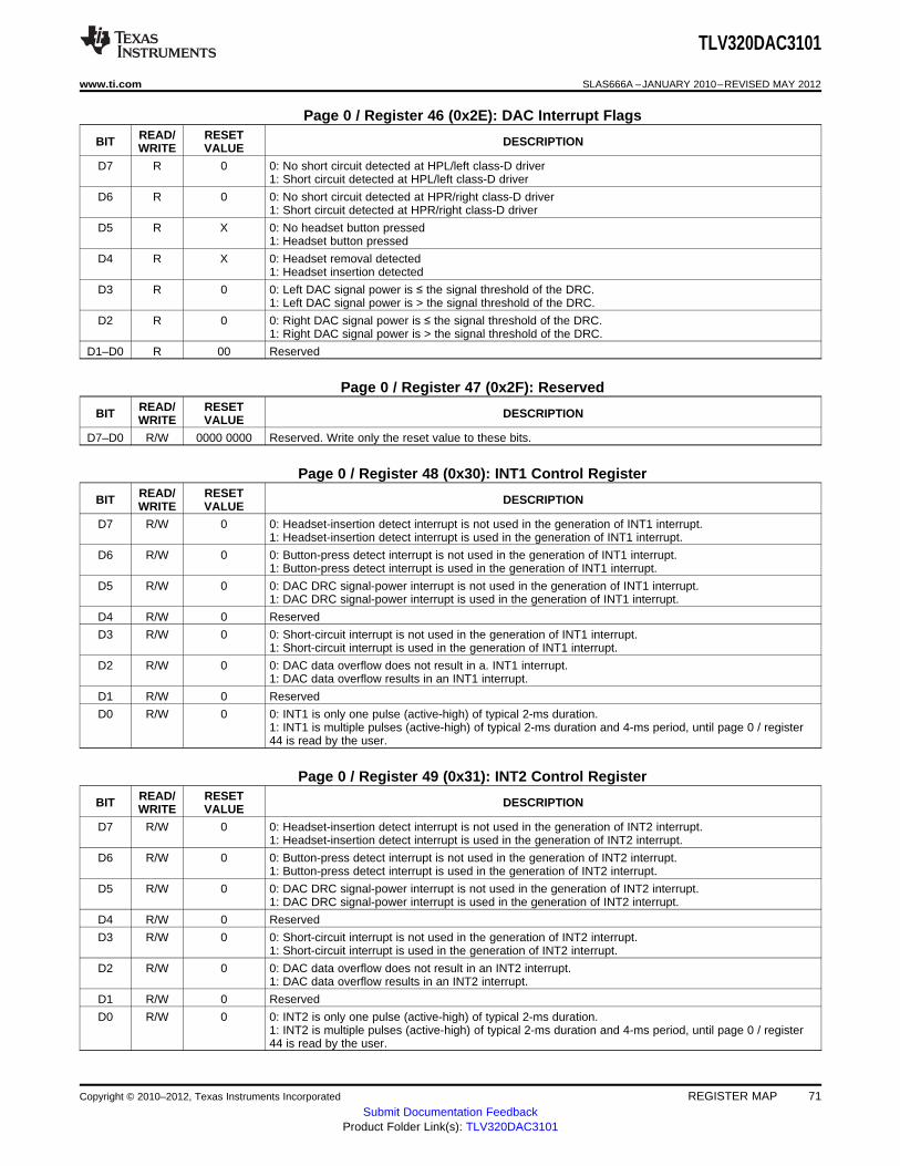
TLV320DAC3101
www.ti.com SLAS666A –JANUARY 2010–REVISED MAY 2012
Page 0 / Register 46 (0x2E): DAC Interrupt FlagsREAD/ RESETBIT DESCRIPTIONWRITE VALUE
D7 R 0 0: No short circuit detected at HPL/left class-D driver1: Short circuit detected at HPL/left class-D driver
D6 R 0 0: No short circuit detected at HPR/right class-D driver1: Short circuit detected at HPR/right class-D driver
D5 R X 0: No headset button pressed1: Headset button pressed
D4 R X 0: Headset removal detected1: Headset insertion detected
D3 R 0 0: Left DAC signal power is ≤ the signal threshold of the DRC.1: Left DAC signal power is > the signal threshold of the DRC.
D2 R 0 0: Right DAC signal power is ≤ the signal threshold of the DRC.1: Right DAC signal power is > the signal threshold of the DRC.
D1–D0 R 00 Reserved
Page 0 / Register 47 (0x2F): ReservedREAD/ RESETBIT DESCRIPTIONWRITE VALUE
D7–D0 R/W 0000 0000 Reserved. Write only the reset value to these bits.
Page 0 / Register 48 (0x30): INT1 Control RegisterREAD/ RESETBIT DESCRIPTIONWRITE VALUE
D7 R/W 0 0: Headset-insertion detect interrupt is not used in the generation of INT1 interrupt.1: Headset-insertion detect interrupt is used in the generation of INT1 interrupt.
D6 R/W 0 0: Button-press detect interrupt is not used in the generation of INT1 interrupt.1: Button-press detect interrupt is used in the generation of INT1 interrupt.
D5 R/W 0 0: DAC DRC signal-power interrupt is not used in the generation of INT1 interrupt.1: DAC DRC signal-power interrupt is used in the generation of INT1 interrupt.
D4 R/W 0 Reserved
D3 R/W 0 0: Short-circuit interrupt is not used in the generation of INT1 interrupt.1: Short-circuit interrupt is used in the generation of INT1 interrupt.
D2 R/W 0 0: DAC data overflow does not result in a. INT1 interrupt.1: DAC data overflow results in an INT1 interrupt.
D1 R/W 0 Reserved
D0 R/W 0 0: INT1 is only one pulse (active-high) of typical 2-ms duration.1: INT1 is multiple pulses (active-high) of typical 2-ms duration and 4-ms period, until page 0 / register44 is read by the user.
Page 0 / Register 49 (0x31): INT2 Control RegisterREAD/ RESETBIT DESCRIPTIONWRITE VALUE
D7 R/W 0 0: Headset-insertion detect interrupt is not used in the generation of INT2 interrupt.1: Headset-insertion detect interrupt is used in the generation of INT2 interrupt.
D6 R/W 0 0: Button-press detect interrupt is not used in the generation of INT2 interrupt.1: Button-press detect interrupt is used in the generation of INT2 interrupt.
D5 R/W 0 0: DAC DRC signal-power interrupt is not used in the generation of INT2 interrupt.1: DAC DRC signal-power interrupt is used in the generation of INT2 interrupt.
D4 R/W 0 Reserved
D3 R/W 0 0: Short-circuit interrupt is not used in the generation of INT2 interrupt.1: Short-circuit interrupt is used in the generation of INT2 interrupt.
D2 R/W 0 0: DAC data overflow does not result in an INT2 interrupt.1: DAC data overflow results in an INT2 interrupt.
D1 R/W 0 Reserved
D0 R/W 0 0: INT2 is only one pulse (active-high) of typical 2-ms duration.1: INT2 is multiple pulses (active-high) of typical 2-ms duration and 4-ms period, until page 0 / register44 is read by the user.
Copyright © 2010–2012, Texas Instruments Incorporated REGISTER MAP 71Submit Documentation Feedback
Product Folder Link(s): TLV320DAC3101
TLV320DAC3101
SLAS666A –JANUARY 2010–REVISED MAY 2012 www.ti.com
Page 0 / Register 50 (0x32): ReservedREAD/ RESETBIT DESCRIPTIONWRITE VALUE
D7-D0 R/W 0000 0000 Reserved. Write only reset values.
Page 0 / Register 51 (0x33): GPIO1 In/Out Pin ControlREAD/ RESETBIT DESCRIPTIONWRITE VALUE
D7–D6 R/W XX Reserved. Do not write any value other than reset value.
D5–D2 R/W 0000 0000: GPIO1 disabled (input and output buffers powered down)0001: GPIO1 is in input mode (can be used as secondary BCLK input, secondary WCLK input,secondary DIN input, or in ClockGen block).0010: GPIO1 is used as general-purpose input (GPI).0011: GPIO1 output = general-purpose output0100: GPIO1 output = CLKOUT output0101: GPIO1 output = INT1 output0110: GPIO1 output = INT2 output0111: Reserved1000: GPIO1 output = secondary BCLK output for codec interface1001: GPIO1 output = secondary WCLK output for codec interface1010: Reserved1011: Reserved1100: Reserved1101: Reserved1110: Reserved1111: Reserved
D1 R X GPIO1 input buffer value
D0 R/W 0 0: GPIO1 general-purpose output value = 01: GPIO1 general-purpose output value = 1
Page 0 / Register 52 (0x34): ReservedREAD/ RESETBIT DESCRIPTIONWRITE VALUE
D7–D0 R/W XX Reserved. Do not write any value other than reset value.
Page 0 / Register 53 (0x35): ReservedREAD/ RESETBIT DESCRIPTIONWRITE VALUE
D7–D0 R/W 0000 0000 Reserved
Page 0 / Register 54 (0x36): DIN (IN Pin) ControlREAD/ RESETBIT DESCRIPTIONWRITE VALUE
D7–D3 R/W 0000 0 Reserved
D2–D1 R/W 01 00: DIN disabled (input buffer powered down)01: DIN enabled (can be used as DIN for codec interface, Dig_Mic_In or in ClockGen block)10: DIN is used as general-purpose input (GPI)11: Reserved
D0 R X DIN input-buffer value
Page 0 / Register 55 (0x37) Through Page 0 / Register 59 (0x3B): ReservedREAD/ RESETBIT DESCRIPTIONWRITE VALUE
D7–D0 R XXXX XXXX Reserved. Do not write to these bits.
72 REGISTER MAP Copyright © 2010–2012, Texas Instruments Incorporated
Submit Documentation FeedbackProduct Folder Link(s): TLV320DAC3101
TLV320DAC3101
www.ti.com SLAS666A –JANUARY 2010–REVISED MAY 2012
Page 0 / Register 60 (0x3C): DAC Processing Block SelectionREAD/ RESETBIT DESCRIPTIONWRITE VALUE
D7–D5 R/W 000 Reserved. Write only default value.
D4–D0 R/W 00 0001 0 0000: Reserved. Do not use.0 0001: DAC Signal Processing Block PRB_P10 0010: DAC Signal Processing Block PRB_P20 0011: DAC Signal Processing Block PRB_P30 0100: DAC Signal Processing Block PRB_P4...1 1000: DAC Signal Processing Block PRB_P241 1001: DAC Signal Processing Block PRB_P251 1010–1 1111: Reserved. Do not use.
Page 0 / Register 61–62: ReservedREAD/ RESETBIT DESCRIPTIONWRITE VALUE
D7–D0 R XXXX XXXX Reserved. Do not write.
Page 0 / Register 63 (0x3F): DAC Data-Path SetupREAD/ RESETBIT DESCRIPTIONWRITE VALUE
D7 R/W 0 0: Left-channel DAC is powered down.1: Left-channel DAC is powered up.
D6 R/W 0 0: Right-channel DAC is powered down.1: Right-channel DAC is powered up.
D5–D4 R/W 01 00: Left-channel DAC data path = off01: Left-channel DAC data path = left data10: Left-channel DAC data path = right data11: Left-channel DAC data path = left-channel and right-channel data ((L + R)/2)
D3–D2 R/W 01 00: Right-channel DAC data path = off01: Right-channel DAC data path = right data10: Right-channel DAC data path = left data11: Right-channel DAC data path = left-channel and right-channel data ((L + R)/2)
D1–D0 R/W 00 00: DAC channel volume control soft-stepping is enabled for one step per sample period.01: DAC channel volume control soft-stepping is enabled for one step per two sample periods.10: DAC channel volume control soft-stepping is disabled.11: Reserved. Do not write this sequence to these bits.
Page 0 / Register 64 (0x40): DAC VOLUME CONTROLREAD/ RESETBIT DESCRIPTIONWRITE VALUE
D7–D4 R/W 0000 Reserved. Write only zeros to these bits.
D3 R/W 1 0: Left-channel DAC not muted1: Left-channel DAC muted
D2 R/W 1 0: Right-channel DAC not muted1: Right-channel DAC muted
D1–D0 R/W 00 (1) 00: Left and right channels have independent volume control.01: Left-channel volume control Is the programmed value of right-channel volume control.10: Right-channel volume control is the programmed value of left-channel volume control.11: Same as 00
(1) When DRC is enabled, left and right channel volume controls are always independent. Program bits D1–D0 to 00.
Copyright © 2010–2012, Texas Instruments Incorporated REGISTER MAP 73Submit Documentation Feedback
Product Folder Link(s): TLV320DAC3101
TLV320DAC3101
SLAS666A –JANUARY 2010–REVISED MAY 2012 www.ti.com
Page 0 / Register 65 (0x41): DAC Left Volume ControlREAD/ RESETBIT DESCRIPTIONWRITE VALUE
D7–D0 R/W 0000 0000 Left DAC Channel Digital Volume Control Setting0111 1111–0011 0001: Reserved. Do not use0011 0000: Digital volume control = 24 dB0010 1111: Digital volume control = 23.5 dB0010 1110: Digital volume control = 23 dB...0000 0001: Digital volume control = 0.5 dB0000 0000: Digital volume control = 0 dB1111 1111: Digital volume control = –0.5 dB...1000 0010: Digital volume control = –63 dB1000 0001: Digital volume control = –63.5 dB1000 0000: Reserved
Page 0 / Register 66 (0x42): DAC Right Volume ControlREAD/ RESETBIT DESCRIPTIONWRITE VALUE
D7–D0 R/W 0000 0000 Right DAC Channel Digital Volume Control Setting0111 1111–0011 0001: Reserved. Do not use0011 0000: Digital volume control = 24 dB0010 1111: Digital volume control = 23.5 dB0010 1110: Digital volume control = 23 dB...0000 0001: Digital volume control = 0.5 dB0000 0000: Digital volume control = 0 dB1111 1111: Digital volume control = –0.5 dB...1000 0010: Digital volume control = –63 dB1000 0001: Digital volume control = –63.5 dB1000 0000: Reserved
Page 0 / Register 67 (0x43): Headset DetectionREAD/ RESETBIT DESCRIPTIONWRITE VALUE
D7 R/W 0 0: Headset detection disabled1: Headset detection enabled
D6–D5 R XX 00: No headset detected01: Headset without microphone is detected10: Reserved11: Headset with microphone is detected
D4–D2 R/W 000 Debounce Programming for Glitch Rejection During Headset Detection (1)
000: 16 ms (sampled with 2-ms clock)001: 32 ms (sampled with 4-ms clock)010: 64 ms (sampled with 8-ms clock)011: 128 ms (sampled with 16-ms clock)100: 256 ms (sampled with 32-ms clock)101: 512 ms (sampled with 64-ms clock)110: Reserved111: Reserved
D1–D0 R/W 00 Debounce Programming for Glitch Rejection During Headset Button-Press Detection00: 0 ms01: 8 ms (sampled with 1-ms clock)10: 16 ms (sampled with 2-ms clock)11: 32 ms (sampled with 4-ms clock)
(1) Note that these times are generated using the 1 MHz reference clock which is defined in page 3 / register 16.
74 REGISTER MAP Copyright © 2010–2012, Texas Instruments Incorporated
Submit Documentation FeedbackProduct Folder Link(s): TLV320DAC3101
TLV320DAC3101
www.ti.com SLAS666A –JANUARY 2010–REVISED MAY 2012
Page 0 / Register 68 (0x44): DRC Control 1READ/ RESETBIT DESCRIPTIONWRITE VALUE
D7 R/W 0 Reserved. Write only the reset value to these bits.
D6 R/W 0 0: DRC disabled for left channel1: DRC enabled for left channel
D5 R/W 0 0: DRC disabled for right channel1: DRC enabled for right channel
D4–D2 R/W 011 000: DRC threshold = –3 dB001: DRC threshold = –6 dB010: DRC threshold = –9 dB011: DRC threshold = –12 dB100: DRC threshold = –15 dB101: DRC threshold = –18 dB110: DRC threshold = –21 dB111: DRC threshold = –24 dB
D1–D0 R/W 11 00: DRC hysteresis = 0 dB01: DRC hysteresis = 1 dB10: DRC hysteresis = 2 dB11: DRC hysteresis = 3 dB
Page 0 / Register 69 (0x45): DRC Control 2READ/ RESETBIT DESCRIPTIONWRITE VALUE
D R 0 Reserved. Write only the reset value to these bits.
D6–D3 R/W 0111 DRC Hold Programmability0000: DRC hold disabled0001:DRC hold time = 32 DAC word clocks0010: DRC hold time = 64 DAC word clocks0011: DRC hold time = 128 DAC word clocks0100: DRC hold time = 256 DAC word clocks0101: DRC hold time = 512 DAC word clocks...1110: DRC hold time = 4 × 32,768 DAC word clocks1111: DRC hold time = 5 × 32,768 DAC word clocks
D2–D0 R 000 Reserved. Write only the reset value to these bits.
Page 0 / Register 70 (0x46): DRC Control 3READ/ RESETBIT DESCRIPTIONWRITE VALUE
D7–D4 R/W 0000 0000: DRC attack rate = 4 dB per DAC word clock0001: DRC attack rate = 2 dB per DAC word clock0010: DRC attack rate = 1 dB per DAC word clock...1110: DRC attack rate = 2.4414e–5 dB per DAC word clock1111: DRC attack rate = 1.2207e–5 dB per DAC word clock
D3–D0 R/W 0000 0000: DRC decay rate = 1.5625e–2 dB per DAC word clock0001: DRC decay rate = 7.8125e–3 dB per DAC word clock0010: DRC decay rate = 3.9062e–3 dB per DAC word clock...1110: DRC decay rate = 9.5367e–7 dB per DAC word clock1111: DRC decay rate = 4.7683e–7 dB per DAC word clock
Copyright © 2010–2012, Texas Instruments Incorporated REGISTER MAP 75Submit Documentation Feedback
Product Folder Link(s): TLV320DAC3101
TLV320DAC3101
SLAS666A –JANUARY 2010–REVISED MAY 2012 www.ti.com
Page 0 / Register 71 (0x47): Left Beep Generator (1)
READ/ RESETBIT DESCRIPTIONWRITE VALUE
D7 R/W 0 0: Beep generator is disabled.1: Beep generator is enabled (self-clearing based on beep duration).
D6 R/W 0 Reserved. Write only reset value.
D5–D0 R/W 00 0000 00 0000: Left-channel beep volume control = 2 dB00 0001: Left-channel beep volume control = 1 dB00 0010: Left-channel beep volume control = 0 dB00 0011: Left-channel beep volume control = –1 dB...11 1110: Left-channel beep volume control = –60 dB11 1111: Left-channel beep volume control = –61 dB
(1) The beep generator is only available in PRB_P25 DAC processing mode.
Page 0 / Register 72 (0x48): Right Beep Generator (1)
READ/ RESETBIT DESCRIPTIONWRITE VALUE
D7–D6 R/W 00 00: Left and right channels have independent beep volume control.01: Left-channel beep volume control is the programmed value of right-channel beep volume control.10: Right-channel beep volume control is the programmed value of left-channel beep volume control.11: Same as 00
D5–D0 R/W 00 0000 00 0000: Right-channel beep volume control = 2 dB00 0001: Right-channel beep volume control = 1 dB00 0010: Right-channel beep volume control = 0 dB00 0011: Right-channel beep volume control = –1 dB...11 1110: Right-channel beep volume control = –60 dB11 1111: Right-channel beep volume control = –61 dB
(1) The beep generator is only available in PRB_P25 DAC processing mode.
Page 0 / Register 73 (0x49): Beep Length MSBREAD/ RESETBIT DESCRIPTIONWRITE VALUE
D7–D0 R/W 0000 0000 8 MSBs out of 24 bits for the number of samples for which the beep must be generated.
Page 0 / Register 74 (0x4A): Beep Length Middle BitsREAD/ RESETBIT DESCRIPTIONWRITE VALUE
D7–D0 R/W 0000 0000 8 middle bits out of 24 bits for the number of samples for which the beep must be generated.
Page 0 / Register 75 (0x4B): Beep Length LSBREAD/ RESETBIT DESCRIPTIONWRITE VALUE
D7–D0 R/W 1110 1110 8 LSBs out of 24 bits for the number of samples for which beep need to be generated.
Page 0 / Register 76 (0x4C): Beep Sin(x) MSBREAD/ RESETBIT DESCRIPTIONWRITE VALUE
D7–D0 R/W 0001 0000 8 MSBs out of 16 bits for sin(2π × fin/fS), where fin is the beep frequency and fS is the DAC sample rate.
Page 0 / Register 77 (0x4D): Beep Sin(x) LSBREAD/ RESETBIT DESCRIPTIONWRITE VALUE
D7–D0 R/W 1101 1000 8 LSBs out of 16 bits for sin(2π × fin/fS), where fin is the beep frequency and fS is the DAC sample rate.
Page 0 / Register 78 (0x4E): Beep Cos(x) MSBREAD/ RESETBIT DESCRIPTIONWRITE VALUE
D7–D0 R/W 0111 1110 8 MSBs out of 16 bits for cos(2π × fin/fS), where fin is the beep frequency and fS is the DAC sample rate.
76 REGISTER MAP Copyright © 2010–2012, Texas Instruments Incorporated
Submit Documentation FeedbackProduct Folder Link(s): TLV320DAC3101
TLV320DAC3101
www.ti.com SLAS666A –JANUARY 2010–REVISED MAY 2012
Page 0 / Register 79 (0x4F): Beep Cos(x) LSBREAD/ RESETBIT DESCRIPTIONWRITE VALUE
D7–D0 R/W 1110 0011 8 LSBs out of 16 bits for cos(2π × fin/fS), where fin is the beep frequency and fS is the DAC sample rate.
Page 0 / Register 80 (0x50) Through Page 0 / Register 115 (0x73): ReservedREAD/ RESETBIT DESCRIPTIONWRITE VALUE
D7–D0 R/W XXXX XXXX Reserved. Do not write to these registers.
Page 0 / Register 116 (0x74): VOL/MICDET-Pin SAR ADC – Volume ControlREAD/ RESETBIT DESCRIPTIONWRITE VALUE
D7 R/W 0 0: DAC volume control is controlled by control register. (7-bit Vol ADC is powered down)1: DAC volume control is controlled by pin.
D6 R/W 0 0: Internal on-chip RC oscillator is used for the 7-bit Vol ADC for pin volume control.1: MCLK is used for the 7-bit Vol ADC for pin volume control.
D5–D4 R/W 00 00: No hysteresis for volume control ADC output01: Hysteresis of ±1 bit10: Hysteresis of ±2 bits11: Reserved. Do not write this sequence to these bits.
D3 R/W 0 Reserved. Write only reset value.
D2–D0 R/W 000 Throughput of the 7-bit Vol ADC for pin volume control, frequency based on MCLK or internal oscillator.
MCLK = 12 MHz Internal Oscillator Source
000: Throughput = 15.625 Hz 10.68 Hz001: Throughput = 31.25 Hz 21.35 Hz010: Throughput = 62.5 Hz 42.71 Hz011: Throughput = 125 Hz 8.2 Hz100: Throughput = 250 Hz 170 Hz101: Throughput = 500 Hz 340 Hz110: Throughput = 1 kHz 680 Hz111: Throughput = 2 kHz 1.37 kHz
Note: These values are based on a nominal oscillatorfrequency of 8.2 MHz. The values scale according tothe actual oscillator frequency.
Page 0 / Register 117 (0x75): VOL/MICDET-Pin GainREAD/ RESETBIT DESCRIPTIONWRITE VALUE
D7 R 0 Reserved. Write only zero to this bit.
D6–D0 R XXX XXXX 000 0000: Gain applied by pin volume control = 18 dB000 0001: Gain applied by pin volume control = 17.5 dB000 0010: Gain applied by pin volume control = 17 dB...010 0011: Gain applied by pin volume control = 0.5 dB010 0100: Gain applied by pin volume control = 0 dB010 0101: Gain applied by pin volume control = –0.5 dB...101 1001: Gain applied by pin volume control = –26.5 dB101 1010: Gain applied by pin volume control = –27 dB101 1011: Gain applied by pin volume control = –28 dB...111 1101: Gain applied by pin volume control = –62 dB111 1110: Gain applied by pin volume control = –63 dB111 1111: Reserved.
Page 0 / Register 118 (0x76) Through Page 0 / Register 127 (0x7F): ReservedREAD/ RESETBIT DESCRIPTIONWRITE VALUE
D7–D0 R/W XXXX XXXX Reserved. Do not write to these registers.
Copyright © 2010–2012, Texas Instruments Incorporated REGISTER MAP 77Submit Documentation Feedback
Product Folder Link(s): TLV320DAC3101
TLV320DAC3101
SLAS666A –JANUARY 2010–REVISED MAY 2012 www.ti.com
6.3 Control Registers, Page 1: DAC, Power-Controls and MISC Logic-RelatedProgrammabilities
Page 1 / Register 0 (0x00): Page Control RegisterREAD/ RESETBIT DESCRIPTIONWRITE VALUE
D7–D0 R/W 0000 0000 0000 0000: Page 0 selected0000 0001: Page 1 selected...1111 1110: Page 254 selected1111 1111: Page 255 selected
Page 1 / Register 1 (0x01) Through Page 1 / Register 29 (0x1D): ReservedREAD/ RESETBIT DESCRIPTIONWRITE VALUE
D7–D0 R/W XXXX XXXX Reserved. Do not write to these registers.
Page 1 / Register 30 (0x1E): Headphone and Speaker Amplifier Error ControlREAD/ RESETBIT DESCRIPTIONWRITE VALUE
D7–D2 R/W 0000 00 Reserved
D1 R/W 0 0: Reset HPL and HPR power-up control bits on short-circuit detection if page 1 / register 31, D1 = 1.1: HPL and HPR power-up control bits remain unchanged on short-circuit detection.
D0 R/W 0 0: Reset SPL and SPR power-up control bits on short-circuit detection.1: SPL and SPR power-up control bits remain unchanged on short-circuit detection.
Page 1 / Register 31 (0x1F): Headphone DriversREAD/ RESETBIT DESCRIPTIONWRITE VALUE
D7 R/W 0 0: HPL output driver is powered down.1: HPL output driver is powered up.
D6 R/W 0 0: HPR output driver is powered down.1: HPR output driver is powered up.
D5 R/W 0 Reserved. Write only zero to this bit.
D4–D3 R/W 0 00: Output common-mode voltage = 1.35 V01: Output common-mode voltage = 1.5 V10: Output common-mode voltage = 1.65 V11: Output common-mode voltage = 1.8 V
D2 R/W 1 Reserved. Write only 1 to this bit.
D1 R/W 0 0: If short-circuit protection is enabled for headphone driver and short circuit is detected, device limitsthe
maximum current to the load.1: If short-circuit protection is enabled for headphone driver and short circuit is detected, device powers
down the output driver.
D0 R 0 0: Short circuit is not detected on the headphone driver.1: Short circuit is detected on the headphone driver.
Page 1 / Register 32 (0x20): Class-D Speaker AmplifierREAD/ RESETBIT DESCRIPTIONWRITE VALUE
D7 R/W 0 0: Left-channel class-D output driver is powered down.1: Left-channel class-D output driver is powered up.
D6 R/W 0 0: Right-channel class-D output driver is powered down.1: Right-channel class-D output driver is powered up.
D5–D1 R/W 00 011 Reserved. Write only the reset value to this bit.
D0 R 0 0: Short circuit is not detected on the class-D driver. Valid only if class-D amplifier is powered up. Forshort-circuit flag sticky bit, see page 0 / register 44.
1: Short circuit is detected on the class-D driver. Valid only if class-D amplifier is powered up. For short-circuit flag sticky bit, see page 0 / register 44.
78 REGISTER MAP Copyright © 2010–2012, Texas Instruments Incorporated
Submit Documentation FeedbackProduct Folder Link(s): TLV320DAC3101
TLV320DAC3101
www.ti.com SLAS666A –JANUARY 2010–REVISED MAY 2012
Page 1 / Register 33 (0x21): HP Output Drivers POP Removal SettingsREAD/ RESETBIT DESCRIPTIONWRITE VALUE
D7 R/W 0 0: If power-down sequence is activated by device software, power down using page 1 / register 46, bitD7, then power down the DAC simultaneously with the HP and SP amplifiers.1: If power-down sequence is activated by device software, power down using page 1 / register 46, bitD7, then power down DAC only after HP and SP amplifiers are completely powered down. This is tooptimize power-down POP.
D6–D3 R/W 0111 0000: Driver power-on time = 0 μs0001: Driver power-on time = 15.3 μs0010: Driver power-on time = 153 μs0011: Driver power-on time = 1.53 ms0100: Driver power-on time = 15.3 ms0101: Driver power-on time = 76.2 ms0110: Driver power-on time = 153 ms0111: Driver power-on time = 304 ms1000: Driver power-on time = 610 ms1001: Driver power-on time = 1.22 s1010: Driver power-on time = 3.04 s1011: Driver power-on time = 6.1 s1100–1111: Reserved. Do not write these sequences to these bits.NOTE: These values are based on typical oscillator frequency of 8.2 MHz. Scale according to the actualoscillator frequency.
D2–D1 R/W 11 00: Driver ramp-up step time = 0 ms01: Driver ramp-up step time = 0.98 ms10: Driver ramp-up step time = 1.95 ms11: Driver ramp-up step time = 3.9 msNOTE: These values are based on typical oscillator frequency of 8.2 MHz. Scale according to the actualoscillator frequency.
D0 R/W 0 0: Weakly driven output common-mode voltage is generated from resistor divider of the AVDD supply.1: Reserved.
Page 1 / Register 34 (0x22): Output Driver PGA Ramp-Down Period ControlREAD/ RESETBIT DESCRIPTIONWRITE VALUE
D7 R/W 0 Reserved. Write only the reset value to this bit.
D6–D4 R/W 000 Speaker Power-Up Wait Time (Duration Based on Using Internal Oscillator)000: Wait time = 0 ms001: Wait time = 3.04 ms010: Wait time = 7.62 ms011: Wait time = 12.2 ms100: Wait time = 15.3 ms101: Wait time = 19.8 ms110: Wait time = 24.4 ms111: Wait time = 30.5 msNOTE: These values are based on typical oscillator frequency of 8.2 MHz. The values scale accordingto the actual oscillator frequency.
D3–D0 R/W 0000 Reserved. Write only the reset value to these bits.
Copyright © 2010–2012, Texas Instruments Incorporated REGISTER MAP 79Submit Documentation Feedback
Product Folder Link(s): TLV320DAC3101
TLV320DAC3101
SLAS666A –JANUARY 2010–REVISED MAY 2012 www.ti.com
Page 1 / Register 35 (0x23): DAC_L and DAC_R Output Mixer RoutingREAD/ RESETBIT DESCRIPTIONWRITE VALUE
D7–D6 R/W 00 00: DAC_L is not routed anywhere.01: DAC_L is routed to the left-channel mixer amplifier.10: DAC_L is routed directly to the HPL driver.11: Reserved
D5 R/W 0 0: AIN1 input is not routed to the left-channel mixer amplifier.1: AIN1 input is routed to the left-channel mixer amplifier.
D4 0 0: AIN2 input is not routed to the left-channel mixer amplifier.1: AIN2 input is routed to the left-channel mixer amplifier.
D3–D2 R/W 00 00: DAC_R is not routed anywhere.01: DAC_R is routed to the right-channel mixer amplifier.10: DAC_R is routed directly to the HPR driver.11: Reserved
D1 R/W 0 0: AIN2 input is not routed to the right-channel mixer amplifier.1: AIN2 input is routed to the right-channel mixer amplifier.
D0 R/W 0 0: HPL driver output is not routed to the HPR driver.1: HPL driver output is routed to the HPR driver input (used for differential output mode).
Page 1 / Register 36 (0x24): Left Analog Vol to HPLREAD/ RESETBIT DESCRIPTIONWRITE VALUE
D7 R/W 0 0: Left-channel analog volume control is not routed to HPL output driver.1: Left-channel analog volume control is routed to HPL output driver.
D6–D0 R/W 111 1111 Left-channel analog volume control gain (non-linear) for the HPL output driver, 0 dB to –78 dB. SeeTable 5-24.
Page 1 / Register 37 (0x25): Right Analog Vol to HPRREAD/ RESETBIT DESCRIPTIONWRITE VALUE
D7 R/W 0 0: Right-channel analog volume control is not routed to HPR output driver.1: Right-channel analog volume control is routed to HPR output driver.
D6–D0 R/W 111 1111 Right-channel analog volume control gain (non-linear) for the HPR output driver, 0 dB to –78 dB. SeeTable 5-24.
Page 1 / Register 38 (0x26): Left Analog Vol to SPLREAD/ RESETBIT DESCRIPTIONWRITE VALUE
D7 R/W 0 0: Left-channel analog volume control output is not routed to left-channel class-D output driver.1: Left-channel analog volume control output is routed to left-channel class-D output driver.
D6–D0 R/W 111 1111 Left-channel analog volume control output gain (non-linear) for the left-channel class-D output driver,0 dB to –78 dB. See Table 5-24.
Page 1 / Register 39 (0x27): Right Analog Vol to SPRREAD/ RESETBIT DESCRIPTIONWRITE VALUE
D7 R/W 0 0: Right-channel analog volume control output is not routed to right-channel class-D output driver.1: Right-channel analog volume control output is routed to right-channel class-D output driver.
D6–D0 R/W 111 1111 Right-channel analog volume control output gain (non-linear) for the right-channel class-D output driver,0 dB to –78 dB. See and Table 5-24.
80 REGISTER MAP Copyright © 2010–2012, Texas Instruments Incorporated
Submit Documentation FeedbackProduct Folder Link(s): TLV320DAC3101
TLV320DAC3101
www.ti.com SLAS666A –JANUARY 2010–REVISED MAY 2012
Page 1 / Register 40 (0x28): HPL DriverREAD/ RESETBIT DESCRIPTIONWRITE VALUE
D7 R/W 0 Reserved. Write only zero to this bit.
D6–D3 R/W 0000 0000: HPL driver PGA = 0 dB0001: HPL driver PGA = 1 dB0010: HPL driver PGA = 2 dB...1000: HPL driver PGA = 8 dB1001: HPL driver PGA = 9 dB1010–1111: Reserved. Do not write these sequences to these bits.
D2 R/W 0 0: HPL driver is muted.1: HPL driver is not muted.
D1 R/W 1 0: HPL driver is weakly driven to a common mode during power down. (1)
1: HPL driver is high-impedance during power down.
D0 R 0 0: Not all programmed gains to HPL have been applied yet.1: All programmed gains to HPL have been applied.
(1) If D1 is programmed as 0, Page 1 / Register 33 D0 must be set to 0.
Page 1 / Register 41 (0x29): HPR DriverREAD/ RESETBIT DESCRIPTIONWRITE VALUE
D7 R/W 0 Reserved. Write only zero to this bit.
D6–D3 R/W 0000 0000: HPR driver PGA = 0 dB0001: HPR driver PGA = 1 dB0010: HPR driver PGA = 2 dB...1000: HPR driver PGA = 8 dB1001: HPR driver PGA = 9 dB1010–1111: Reserved. Do not write these sequences to these bits.
D2 R/W 0 0: HPR driver is muted.1: HPR driver is not muted.
D1 R/W 1 0: HPR driver is weakly driven to a common mode during power down. (1)
1: HPR driver is high-impedance during power down.
D0 R 0 0: Not all programmed gains to HPR have been applied yet.1: All programmed gains to HPR have been applied.
(1) If D1 is programmed as 0, Page 1 / Register 33 D0 must be set to 0.
Page 1 / Register 42 (0x2A): SPL DriverREAD/ RESETBIT DESCRIPTIONWRITE VALUE
D7–D5 R/W 000 Reserved. Write only zeros to these bits.
D4–D3 R/W 00 00: Left-channel class-D driver output stage gain = 6 dB01: Left-channel class-D driver output stage gain = 12 dB10: Left-channel class-D driver output stage gain = 18 dB11: Left-channel class-D driver output stage gain = 24 dB
D2 R/W 0 0: Left-channel class-D driver is muted.1: Left-channel class-D driver is not muted.
D1 R/W 0 Reserved. Write only zero to this bit.
D0 R 0 0: Not all programmed gains to left-channel class-D driver have been applied yet.1: All programmed gains to left-channel class-D driver have been applied.
Copyright © 2010–2012, Texas Instruments Incorporated REGISTER MAP 81Submit Documentation Feedback
Product Folder Link(s): TLV320DAC3101
TLV320DAC3101
SLAS666A –JANUARY 2010–REVISED MAY 2012 www.ti.com
Page 1 / Register 43 (0x2B): SPR DriverREAD/ RESETBIT DESCRIPTIONWRITE VALUE
D7–D5 R/W 000 Reserved. Write only zeros to these bits.
D4–D3 R/W 00 00: Right-channel class-D driver output stage gain = 6 dB01: Right-channel class-D driver output stage gain = 12 dB10: Right-channel class-D driver output stage gain = 18 dB11: Right-channel class-D driver output stage gain = 24 dB
D2 R/W 0 0: Right-channel class-D driver is muted.1: Right-channel class-D driver is not muted.
D1 R/W 0 Reserved. Write only zero to this bit.
D0 R 0 0: Not all programmed gains to right-channel class-D driver have been applied yet.1: All programmed gains to right-channel class-D driver have been applied.
Page 1 / Register 44 (0x2C): HP Driver ControlREAD/ RESETBIT DESCRIPTIONWRITE VALUE
D7–D5 R/W 000 Debounce Time for Headset Short-Circuit Detection
MCLK/DIV (Page 3 /(1) register 16) = 1-MHz Internal Oscillator Source
Source
000: Debounce time = 0 μs 0 μs001: Debounce time = 8 μs 7.8 μs010: Debounce time = 16 μs 15.6 μs011: Debounce time = 32 μs 31.2 μs100: Debounce time = 64 μs 62.4 μs101: Debounce time = 128 μs 124.9 μs110: Debounce time = 256 μs 250 μs111: Debounce time = 512 μs 500 μs
Note: These values are based on a nominal oscillatorfrequency of 8.2 MHz. The values scale according tothe actual oscillator frequency.
D4–D3 R/W 00 00: Default mode for the DAC01: DAC performance increased by increasing the current10: Reserved11: DAC performance increased further by increasing the current again
D2 R/W 0 0: HPL output driver is programmed as headphone driver.1: HPL output driver is programmed as lineout driver.
D1 R/W 0 0: HPR output driver is programmed as headphone driver.1: HPR output driver is programmed as lineout driver.
D0 R/W 0 Reserved. Write only zero to this bit.
(1) The clock used for the debounce has a clock period = debounce duration/8.
Page 1 / Register 45 (0x2D): ReservedREAD/ RESETBIT DESCRIPTIONWRITE VALUE
D7–D0 R/W XXXX XXXX Reserved. Do not write to these registers.
Page 1 / Register 46 (0x2E): MICBIASREAD/ RESETBIT DESCRIPTIONWRITE VALUE
D7 R/W 0 0: Device software power down is not enabled.1: Device software power down is enabled.
D6–D4 R/W 000 Reserved. Write only zeros to these bits.
D3 R/W 0 0: Programmed MICBIAS is not powered up if headset detection is enabled but headset is not inserted.1: Programmed MICBIAS is powered up even if headset is not inserted.
D2 R/W 0 Reserved. Write only zero to this bit.
D1–D0 R/W 00 00: MICBIAS output is powered down.01: MICBIAS output is powered to 2 V.10: MICBIAS output is powered to 2.5 V.11: MICBIAS output is powered to AVDD.
82 REGISTER MAP Copyright © 2010–2012, Texas Instruments Incorporated
Submit Documentation FeedbackProduct Folder Link(s): TLV320DAC3101
TLV320DAC3101
www.ti.com SLAS666A –JANUARY 2010–REVISED MAY 2012
Page 1 / Register 47 (0x2F) Through Page 1 / Register 49 (0x31): ReservedREAD/ RESETBIT DESCRIPTIONWRITE VALUE
D7–D0 R XXXX XXXX Reserved. Do not write to these bits.
Page 1 / Register 50 (0x32): Input CM SettingsREAD/ RESETBIT DESCRIPTIONWRITE VALUE
D7 R/W 0 0: AIN1 input is floating if it is not used for analog bypass.1: AIN1 input is connected to CM internally if it is not used for analog bypass.
D6 R/W 0 0: AIN2 input is floating if it is not used for analog bypass.1: AIN2 input is connected to CM internally if it is not used for analog bypass.
D5–D0 R/W 000000 Reserved. Write only zeros to these bits.
Page 1 / Register 51 (0x33) Through Page 1 / Register 127 (0x7F): ReservedREAD/ RESETBIT DESCRIPTIONWRITE VALUE
D7–D0 R/W XXXX XXXX Reserved. Write only the reset value to these bits.
6.4 Control Registers, Page 3: MCLK Divider for Programmable Delay Timer
Default values shown for this page only become valid 100 μs following a hardware or software reset.
Page 3 / Register 0 (0x00): Page Control RegisterREAD/ RESETBIT DESCRIPTIONWRITE VALUE
D7–D0 R/W 0000 0000 0000 0000: Page 0 selected0000 0001: Page 1 selected...1111 1110: Page 254 selected1111 1111: Page 255 selected
The only register used in page 3 is register 16. The remaining page-3 registers are reserved and shouldnot be written to.
Page 3 / Register 16 (0x10): Timer Clock MCLK DividerREAD/ RESETBIT DESCRIPTIONWRITE VALUE
D7 R/W 1 0: Internal oscillator is used for programmable delay timer.1: External MCLK (1) is used for programmable delay timer.
D6–D0 R/W 0000 0001 MCLK Divider to Generate 1-MHz Clock for the Programmable Delay Timer000 0000: MCLK divider = 128000 0001: MCLK divider = 1000 0010: MCLK divider = 2...111 1110: MCLK divider = 126111 1111: MCLK divider = 127
(1) External clock is used only to control the delay programmed between the conversions and not used for doing the actual conversion. Thisfeature is provided in case a more accurate delay is desired, because the internal oscillator frequency varies from device to device.
6.5 Control Registers, Page 8: DAC Programmable Coefficients RAM Buffer A (1:63)
Default values shown for this page only become valid 100 μs following a hardware or software reset.
Page 8 / Register 0 (0x00): Page Control RegisterREAD/ RESETBIT DESCRIPTIONWRITE VALUE
D7–D0 R/W 0000 0000 0000 0000: Page 0 selected0000 0001: Page 1 selected...1111 1110: Page 254 selected1111 1111: Page 255 selected
Copyright © 2010–2012, Texas Instruments Incorporated REGISTER MAP 83Submit Documentation Feedback
Product Folder Link(s): TLV320DAC3101
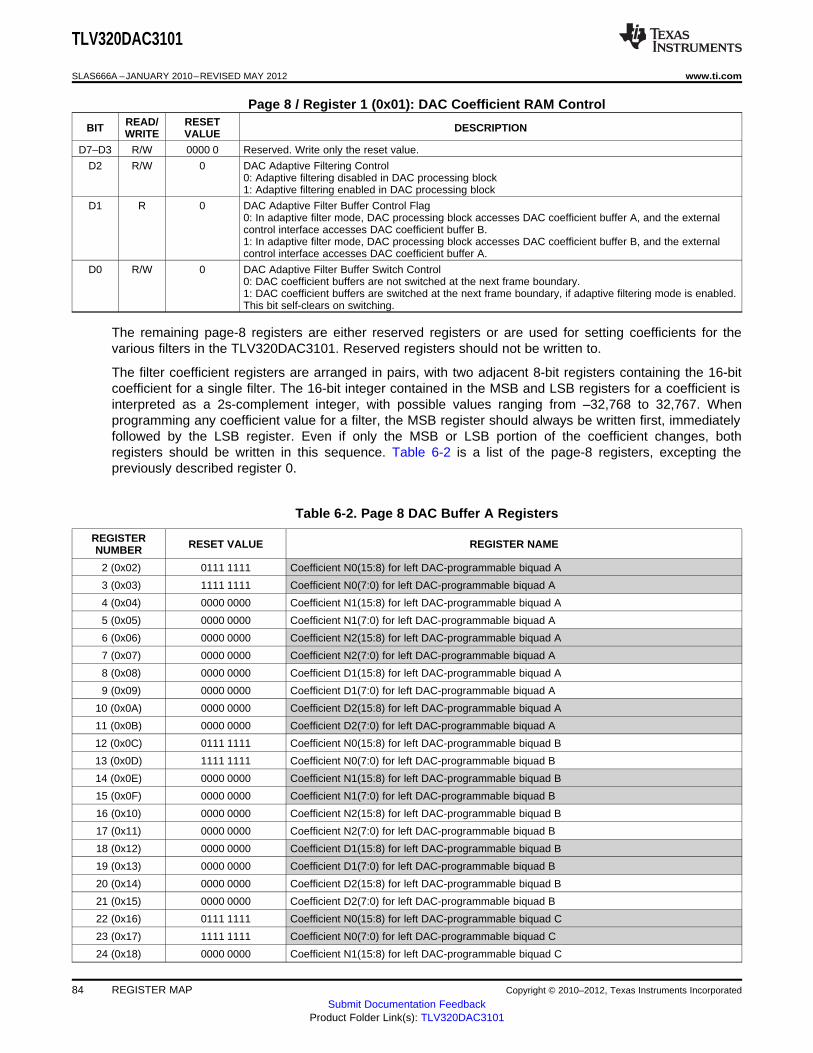
TLV320DAC3101
SLAS666A –JANUARY 2010–REVISED MAY 2012 www.ti.com
Page 8 / Register 1 (0x01): DAC Coefficient RAM ControlREAD/ RESETBIT DESCRIPTIONWRITE VALUE
D7–D3 R/W 0000 0 Reserved. Write only the reset value.
D2 R/W 0 DAC Adaptive Filtering Control0: Adaptive filtering disabled in DAC processing block1: Adaptive filtering enabled in DAC processing block
D1 R 0 DAC Adaptive Filter Buffer Control Flag0: In adaptive filter mode, DAC processing block accesses DAC coefficient buffer A, and the externalcontrol interface accesses DAC coefficient buffer B.1: In adaptive filter mode, DAC processing block accesses DAC coefficient buffer B, and the externalcontrol interface accesses DAC coefficient buffer A.
D0 R/W 0 DAC Adaptive Filter Buffer Switch Control0: DAC coefficient buffers are not switched at the next frame boundary.1: DAC coefficient buffers are switched at the next frame boundary, if adaptive filtering mode is enabled.This bit self-clears on switching.
The remaining page-8 registers are either reserved registers or are used for setting coefficients for thevarious filters in the TLV320DAC3101. Reserved registers should not be written to.
The filter coefficient registers are arranged in pairs, with two adjacent 8-bit registers containing the 16-bitcoefficient for a single filter. The 16-bit integer contained in the MSB and LSB registers for a coefficient isinterpreted as a 2s-complement integer, with possible values ranging from –32,768 to 32,767. Whenprogramming any coefficient value for a filter, the MSB register should always be written first, immediatelyfollowed by the LSB register. Even if only the MSB or LSB portion of the coefficient changes, bothregisters should be written in this sequence. Table 6-2 is a list of the page-8 registers, excepting thepreviously described register 0.
Table 6-2. Page 8 DAC Buffer A Registers
REGISTER RESET VALUE REGISTER NAMENUMBER
2 (0x02) 0111 1111 Coefficient N0(15:8) for left DAC-programmable biquad A
3 (0x03) 1111 1111 Coefficient N0(7:0) for left DAC-programmable biquad A
4 (0x04) 0000 0000 Coefficient N1(15:8) for left DAC-programmable biquad A
5 (0x05) 0000 0000 Coefficient N1(7:0) for left DAC-programmable biquad A
6 (0x06) 0000 0000 Coefficient N2(15:8) for left DAC-programmable biquad A
7 (0x07) 0000 0000 Coefficient N2(7:0) for left DAC-programmable biquad A
8 (0x08) 0000 0000 Coefficient D1(15:8) for left DAC-programmable biquad A
9 (0x09) 0000 0000 Coefficient D1(7:0) for left DAC-programmable biquad A
10 (0x0A) 0000 0000 Coefficient D2(15:8) for left DAC-programmable biquad A
11 (0x0B) 0000 0000 Coefficient D2(7:0) for left DAC-programmable biquad A
12 (0x0C) 0111 1111 Coefficient N0(15:8) for left DAC-programmable biquad B
13 (0x0D) 1111 1111 Coefficient N0(7:0) for left DAC-programmable biquad B
14 (0x0E) 0000 0000 Coefficient N1(15:8) for left DAC-programmable biquad B
15 (0x0F) 0000 0000 Coefficient N1(7:0) for left DAC-programmable biquad B
16 (0x10) 0000 0000 Coefficient N2(15:8) for left DAC-programmable biquad B
17 (0x11) 0000 0000 Coefficient N2(7:0) for left DAC-programmable biquad B
18 (0x12) 0000 0000 Coefficient D1(15:8) for left DAC-programmable biquad B
19 (0x13) 0000 0000 Coefficient D1(7:0) for left DAC-programmable biquad B
20 (0x14) 0000 0000 Coefficient D2(15:8) for left DAC-programmable biquad B
21 (0x15) 0000 0000 Coefficient D2(7:0) for left DAC-programmable biquad B
22 (0x16) 0111 1111 Coefficient N0(15:8) for left DAC-programmable biquad C
23 (0x17) 1111 1111 Coefficient N0(7:0) for left DAC-programmable biquad C
24 (0x18) 0000 0000 Coefficient N1(15:8) for left DAC-programmable biquad C
84 REGISTER MAP Copyright © 2010–2012, Texas Instruments Incorporated
Submit Documentation FeedbackProduct Folder Link(s): TLV320DAC3101
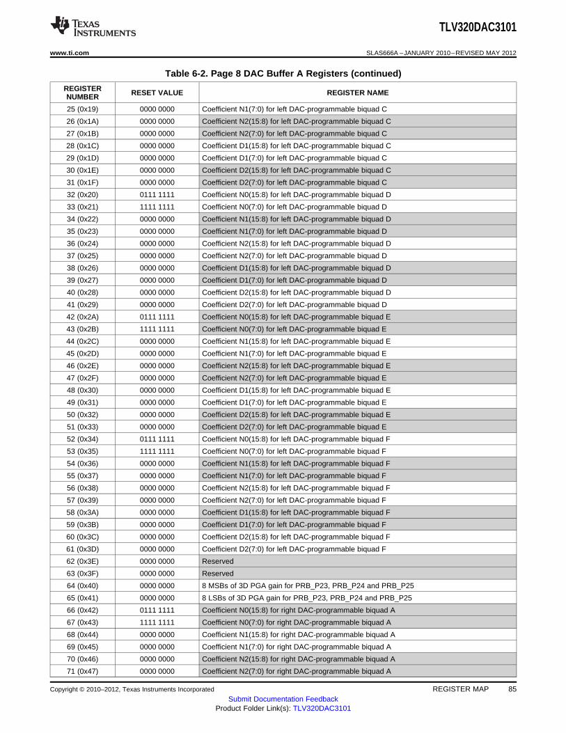
TLV320DAC3101
www.ti.com SLAS666A –JANUARY 2010–REVISED MAY 2012
Table 6-2. Page 8 DAC Buffer A Registers (continued)
REGISTER RESET VALUE REGISTER NAMENUMBER
25 (0x19) 0000 0000 Coefficient N1(7:0) for left DAC-programmable biquad C
26 (0x1A) 0000 0000 Coefficient N2(15:8) for left DAC-programmable biquad C
27 (0x1B) 0000 0000 Coefficient N2(7:0) for left DAC-programmable biquad C
28 (0x1C) 0000 0000 Coefficient D1(15:8) for left DAC-programmable biquad C
29 (0x1D) 0000 0000 Coefficient D1(7:0) for left DAC-programmable biquad C
30 (0x1E) 0000 0000 Coefficient D2(15:8) for left DAC-programmable biquad C
31 (0x1F) 0000 0000 Coefficient D2(7:0) for left DAC-programmable biquad C
32 (0x20) 0111 1111 Coefficient N0(15:8) for left DAC-programmable biquad D
33 (0x21) 1111 1111 Coefficient N0(7:0) for left DAC-programmable biquad D
34 (0x22) 0000 0000 Coefficient N1(15:8) for left DAC-programmable biquad D
35 (0x23) 0000 0000 Coefficient N1(7:0) for left DAC-programmable biquad D
36 (0x24) 0000 0000 Coefficient N2(15:8) for left DAC-programmable biquad D
37 (0x25) 0000 0000 Coefficient N2(7:0) for left DAC-programmable biquad D
38 (0x26) 0000 0000 Coefficient D1(15:8) for left DAC-programmable biquad D
39 (0x27) 0000 0000 Coefficient D1(7:0) for left DAC-programmable biquad D
40 (0x28) 0000 0000 Coefficient D2(15:8) for left DAC-programmable biquad D
41 (0x29) 0000 0000 Coefficient D2(7:0) for left DAC-programmable biquad D
42 (0x2A) 0111 1111 Coefficient N0(15:8) for left DAC-programmable biquad E
43 (0x2B) 1111 1111 Coefficient N0(7:0) for left DAC-programmable biquad E
44 (0x2C) 0000 0000 Coefficient N1(15:8) for left DAC-programmable biquad E
45 (0x2D) 0000 0000 Coefficient N1(7:0) for left DAC-programmable biquad E
46 (0x2E) 0000 0000 Coefficient N2(15:8) for left DAC-programmable biquad E
47 (0x2F) 0000 0000 Coefficient N2(7:0) for left DAC-programmable biquad E
48 (0x30) 0000 0000 Coefficient D1(15:8) for left DAC-programmable biquad E
49 (0x31) 0000 0000 Coefficient D1(7:0) for left DAC-programmable biquad E
50 (0x32) 0000 0000 Coefficient D2(15:8) for left DAC-programmable biquad E
51 (0x33) 0000 0000 Coefficient D2(7:0) for left DAC-programmable biquad E
52 (0x34) 0111 1111 Coefficient N0(15:8) for left DAC-programmable biquad F
53 (0x35) 1111 1111 Coefficient N0(7:0) for left DAC-programmable biquad F
54 (0x36) 0000 0000 Coefficient N1(15:8) for left DAC-programmable biquad F
55 (0x37) 0000 0000 Coefficient N1(7:0) for left DAC-programmable biquad F
56 (0x38) 0000 0000 Coefficient N2(15:8) for left DAC-programmable biquad F
57 (0x39) 0000 0000 Coefficient N2(7:0) for left DAC-programmable biquad F
58 (0x3A) 0000 0000 Coefficient D1(15:8) for left DAC-programmable biquad F
59 (0x3B) 0000 0000 Coefficient D1(7:0) for left DAC-programmable biquad F
60 (0x3C) 0000 0000 Coefficient D2(15:8) for left DAC-programmable biquad F
61 (0x3D) 0000 0000 Coefficient D2(7:0) for left DAC-programmable biquad F
62 (0x3E) 0000 0000 Reserved
63 (0x3F) 0000 0000 Reserved
64 (0x40) 0000 0000 8 MSBs of 3D PGA gain for PRB_P23, PRB_P24 and PRB_P25
65 (0x41) 0000 0000 8 LSBs of 3D PGA gain for PRB_P23, PRB_P24 and PRB_P25
66 (0x42) 0111 1111 Coefficient N0(15:8) for right DAC-programmable biquad A
67 (0x43) 1111 1111 Coefficient N0(7:0) for right DAC-programmable biquad A
68 (0x44) 0000 0000 Coefficient N1(15:8) for right DAC-programmable biquad A
69 (0x45) 0000 0000 Coefficient N1(7:0) for right DAC-programmable biquad A
70 (0x46) 0000 0000 Coefficient N2(15:8) for right DAC-programmable biquad A
71 (0x47) 0000 0000 Coefficient N2(7:0) for right DAC-programmable biquad A
Copyright © 2010–2012, Texas Instruments Incorporated REGISTER MAP 85Submit Documentation Feedback
Product Folder Link(s): TLV320DAC3101
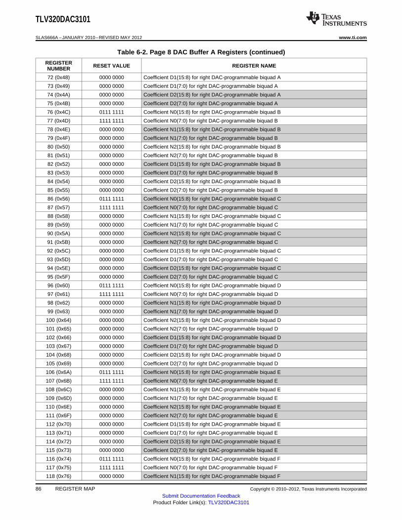
TLV320DAC3101
SLAS666A –JANUARY 2010–REVISED MAY 2012 www.ti.com
Table 6-2. Page 8 DAC Buffer A Registers (continued)
REGISTER RESET VALUE REGISTER NAMENUMBER
72 (0x48) 0000 0000 Coefficient D1(15:8) for right DAC-programmable biquad A
73 (0x49) 0000 0000 Coefficient D1(7:0) for right DAC-programmable biquad A
74 (0x4A) 0000 0000 Coefficient D2(15:8) for right DAC-programmable biquad A
75 (0x4B) 0000 0000 Coefficient D2(7:0) for right DAC-programmable biquad A
76 (0x4C) 0111 1111 Coefficient N0(15:8) for right DAC-programmable biquad B
77 (0x4D) 1111 1111 Coefficient N0(7:0) for right DAC-programmable biquad B
78 (0x4E) 0000 0000 Coefficient N1(15:8) for right DAC-programmable biquad B
79 (0x4F) 0000 0000 Coefficient N1(7:0) for right DAC-programmable biquad B
80 (0x50) 0000 0000 Coefficient N2(15:8) for right DAC-programmable biquad B
81 (0x51) 0000 0000 Coefficient N2(7:0) for right DAC-programmable biquad B
82 (0x52) 0000 0000 Coefficient D1(15:8) for right DAC-programmable biquad B
83 (0x53) 0000 0000 Coefficient D1(7:0) for right DAC-programmable biquad B
84 (0x54) 0000 0000 Coefficient D2(15:8) for right DAC-programmable biquad B
85 (0x55) 0000 0000 Coefficient D2(7:0) for right DAC-programmable biquad B
86 (0x56) 0111 1111 Coefficient N0(15:8) for right DAC-programmable biquad C
87 (0x57) 1111 1111 Coefficient N0(7:0) for right DAC-programmable biquad C
88 (0x58) 0000 0000 Coefficient N1(15:8) for right DAC-programmable biquad C
89 (0x59) 0000 0000 Coefficient N1(7:0) for right DAC-programmable biquad C
90 (0x5A) 0000 0000 Coefficient N2(15:8) for right DAC-programmable biquad C
91 (0x5B) 0000 0000 Coefficient N2(7:0) for right DAC-programmable biquad C
92 (0x5C) 0000 0000 Coefficient D1(15:8) for right DAC-programmable biquad C
93 (0x5D) 0000 0000 Coefficient D1(7:0) for right DAC-programmable biquad C
94 (0x5E) 0000 0000 Coefficient D2(15:8) for right DAC-programmable biquad C
95 (0x5F) 0000 0000 Coefficient D2(7:0) for right DAC-programmable biquad C
96 (0x60) 0111 1111 Coefficient N0(15:8) for right DAC-programmable biquad D
97 (0x61) 1111 1111 Coefficient N0(7:0) for right DAC-programmable biquad D
98 (0x62) 0000 0000 Coefficient N1(15:8) for right DAC-programmable biquad D
99 (0x63) 0000 0000 Coefficient N1(7:0) for right DAC-programmable biquad D
100 (0x64) 0000 0000 Coefficient N2(15:8) for right DAC-programmable biquad D
101 (0x65) 0000 0000 Coefficient N2(7:0) for right DAC-programmable biquad D
102 (0x66) 0000 0000 Coefficient D1(15:8) for right DAC-programmable biquad D
103 (0x67) 0000 0000 Coefficient D1(7:0) for right DAC-programmable biquad D
104 (0x68) 0000 0000 Coefficient D2(15:8) for right DAC-programmable biquad D
105 (0x69) 0000 0000 Coefficient D2(7:0) for right DAC-programmable biquad D
106 (0x6A) 0111 1111 Coefficient N0(15:8) for right DAC-programmable biquad E
107 (0x6B) 1111 1111 Coefficient N0(7:0) for right DAC-programmable biquad E
108 (0x6C) 0000 0000 Coefficient N1(15:8) for right DAC-programmable biquad E
109 (0x6D) 0000 0000 Coefficient N1(7:0) for right DAC-programmable biquad E
110 (0x6E) 0000 0000 Coefficient N2(15:8) for right DAC-programmable biquad E
111 (0x6F) 0000 0000 Coefficient N2(7:0) for right DAC-programmable biquad E
112 (0x70) 0000 0000 Coefficient D1(15:8) for right DAC-programmable biquad E
113 (0x71) 0000 0000 Coefficient D1(7:0) for right DAC-programmable biquad E
114 (0x72) 0000 0000 Coefficient D2(15:8) for right DAC-programmable biquad E
115 (0x73) 0000 0000 Coefficient D2(7:0) for right DAC-programmable biquad E
116 (0x74) 0111 1111 Coefficient N0(15:8) for right DAC-programmable biquad F
117 (0x75) 1111 1111 Coefficient N0(7:0) for right DAC-programmable biquad F
118 (0x76) 0000 0000 Coefficient N1(15:8) for right DAC-programmable biquad F
86 REGISTER MAP Copyright © 2010–2012, Texas Instruments Incorporated
Submit Documentation FeedbackProduct Folder Link(s): TLV320DAC3101
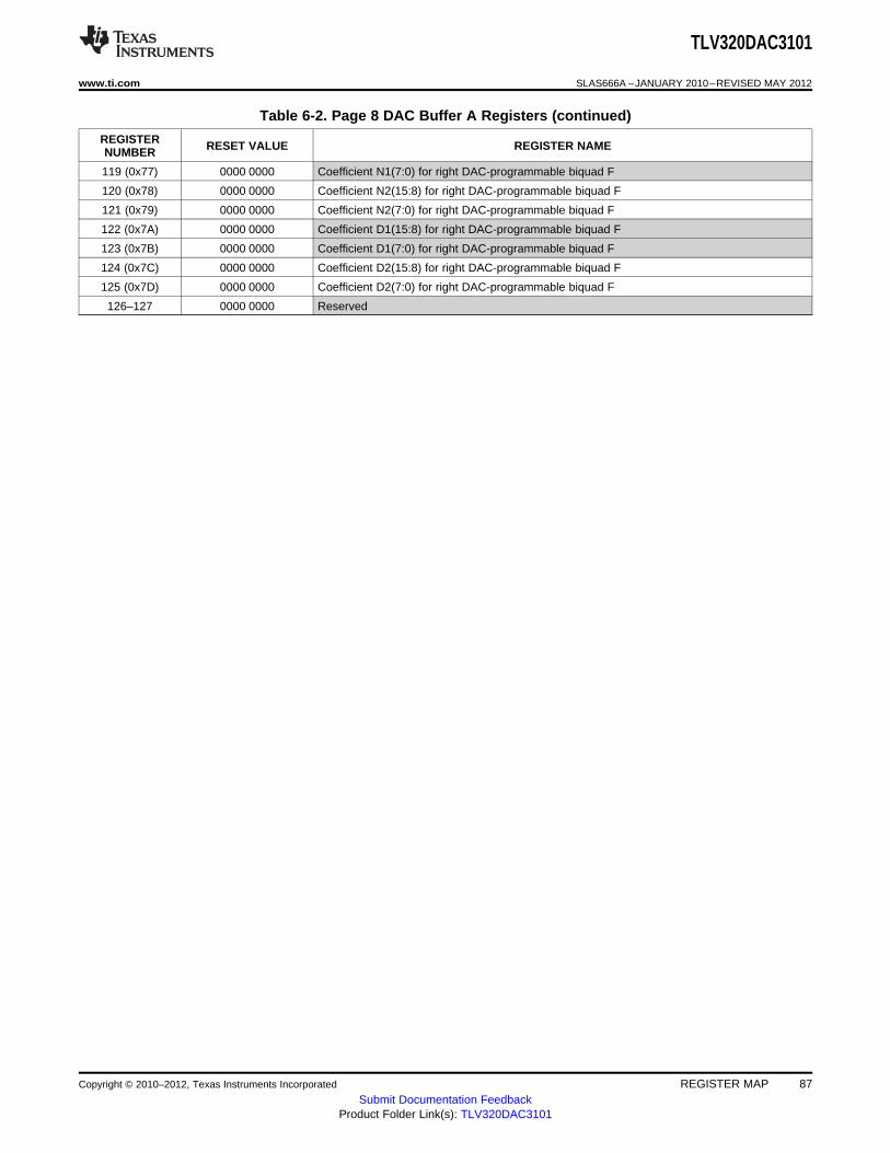
TLV320DAC3101
www.ti.com SLAS666A –JANUARY 2010–REVISED MAY 2012
Table 6-2. Page 8 DAC Buffer A Registers (continued)
REGISTER RESET VALUE REGISTER NAMENUMBER
119 (0x77) 0000 0000 Coefficient N1(7:0) for right DAC-programmable biquad F
120 (0x78) 0000 0000 Coefficient N2(15:8) for right DAC-programmable biquad F
121 (0x79) 0000 0000 Coefficient N2(7:0) for right DAC-programmable biquad F
122 (0x7A) 0000 0000 Coefficient D1(15:8) for right DAC-programmable biquad F
123 (0x7B) 0000 0000 Coefficient D1(7:0) for right DAC-programmable biquad F
124 (0x7C) 0000 0000 Coefficient D2(15:8) for right DAC-programmable biquad F
125 (0x7D) 0000 0000 Coefficient D2(7:0) for right DAC-programmable biquad F
126–127 0000 0000 Reserved
Copyright © 2010–2012, Texas Instruments Incorporated REGISTER MAP 87Submit Documentation Feedback
Product Folder Link(s): TLV320DAC3101
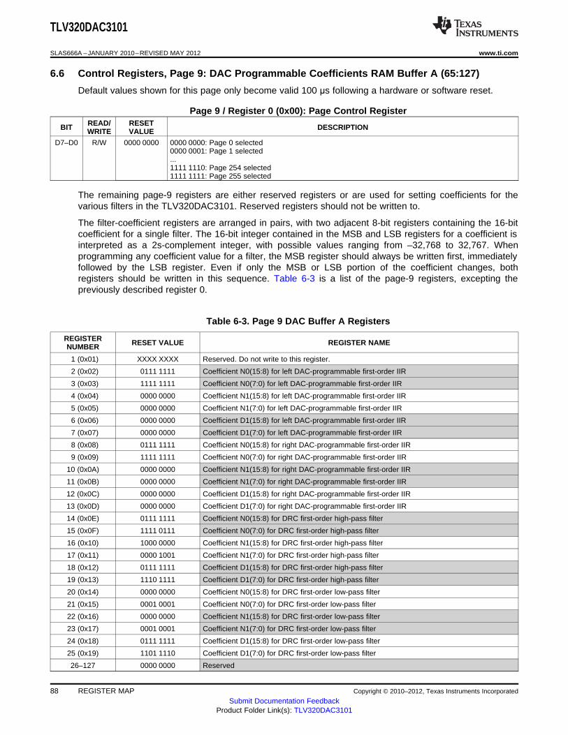
TLV320DAC3101
SLAS666A –JANUARY 2010–REVISED MAY 2012 www.ti.com
6.6 Control Registers, Page 9: DAC Programmable Coefficients RAM Buffer A (65:127)
Default values shown for this page only become valid 100 μs following a hardware or software reset.
Page 9 / Register 0 (0x00): Page Control RegisterREAD/ RESETBIT DESCRIPTIONWRITE VALUE
D7–D0 R/W 0000 0000 0000 0000: Page 0 selected0000 0001: Page 1 selected...1111 1110: Page 254 selected1111 1111: Page 255 selected
The remaining page-9 registers are either reserved registers or are used for setting coefficients for thevarious filters in the TLV320DAC3101. Reserved registers should not be written to.
The filter-coefficient registers are arranged in pairs, with two adjacent 8-bit registers containing the 16-bitcoefficient for a single filter. The 16-bit integer contained in the MSB and LSB registers for a coefficient isinterpreted as a 2s-complement integer, with possible values ranging from –32,768 to 32,767. Whenprogramming any coefficient value for a filter, the MSB register should always be written first, immediatelyfollowed by the LSB register. Even if only the MSB or LSB portion of the coefficient changes, bothregisters should be written in this sequence. Table 6-3 is a list of the page-9 registers, excepting thepreviously described register 0.
Table 6-3. Page 9 DAC Buffer A Registers
REGISTER RESET VALUE REGISTER NAMENUMBER
1 (0x01) XXXX XXXX Reserved. Do not write to this register.
2 (0x02) 0111 1111 Coefficient N0(15:8) for left DAC-programmable first-order IIR
3 (0x03) 1111 1111 Coefficient N0(7:0) for left DAC-programmable first-order IIR
4 (0x04) 0000 0000 Coefficient N1(15:8) for left DAC-programmable first-order IIR
5 (0x05) 0000 0000 Coefficient N1(7:0) for left DAC-programmable first-order IIR
6 (0x06) 0000 0000 Coefficient D1(15:8) for left DAC-programmable first-order IIR
7 (0x07) 0000 0000 Coefficient D1(7:0) for left DAC-programmable first-order IIR
8 (0x08) 0111 1111 Coefficient N0(15:8) for right DAC-programmable first-order IIR
9 (0x09) 1111 1111 Coefficient N0(7:0) for right DAC-programmable first-order IIR
10 (0x0A) 0000 0000 Coefficient N1(15:8) for right DAC-programmable first-order IIR
11 (0x0B) 0000 0000 Coefficient N1(7:0) for right DAC-programmable first-order IIR
12 (0x0C) 0000 0000 Coefficient D1(15:8) for right DAC-programmable first-order IIR
13 (0x0D) 0000 0000 Coefficient D1(7:0) for right DAC-programmable first-order IIR
14 (0x0E) 0111 1111 Coefficient N0(15:8) for DRC first-order high-pass filter
15 (0x0F) 1111 0111 Coefficient N0(7:0) for DRC first-order high-pass filter
16 (0x10) 1000 0000 Coefficient N1(15:8) for DRC first-order high-pass filter
17 (0x11) 0000 1001 Coefficient N1(7:0) for DRC first-order high-pass filter
18 (0x12) 0111 1111 Coefficient D1(15:8) for DRC first-order high-pass filter
19 (0x13) 1110 1111 Coefficient D1(7:0) for DRC first-order high-pass filter
20 (0x14) 0000 0000 Coefficient N0(15:8) for DRC first-order low-pass filter
21 (0x15) 0001 0001 Coefficient N0(7:0) for DRC first-order low-pass filter
22 (0x16) 0000 0000 Coefficient N1(15:8) for DRC first-order low-pass filter
23 (0x17) 0001 0001 Coefficient N1(7:0) for DRC first-order low-pass filter
24 (0x18) 0111 1111 Coefficient D1(15:8) for DRC first-order low-pass filter
25 (0x19) 1101 1110 Coefficient D1(7:0) for DRC first-order low-pass filter
26–127 0000 0000 Reserved
88 REGISTER MAP Copyright © 2010–2012, Texas Instruments Incorporated
Submit Documentation FeedbackProduct Folder Link(s): TLV320DAC3101
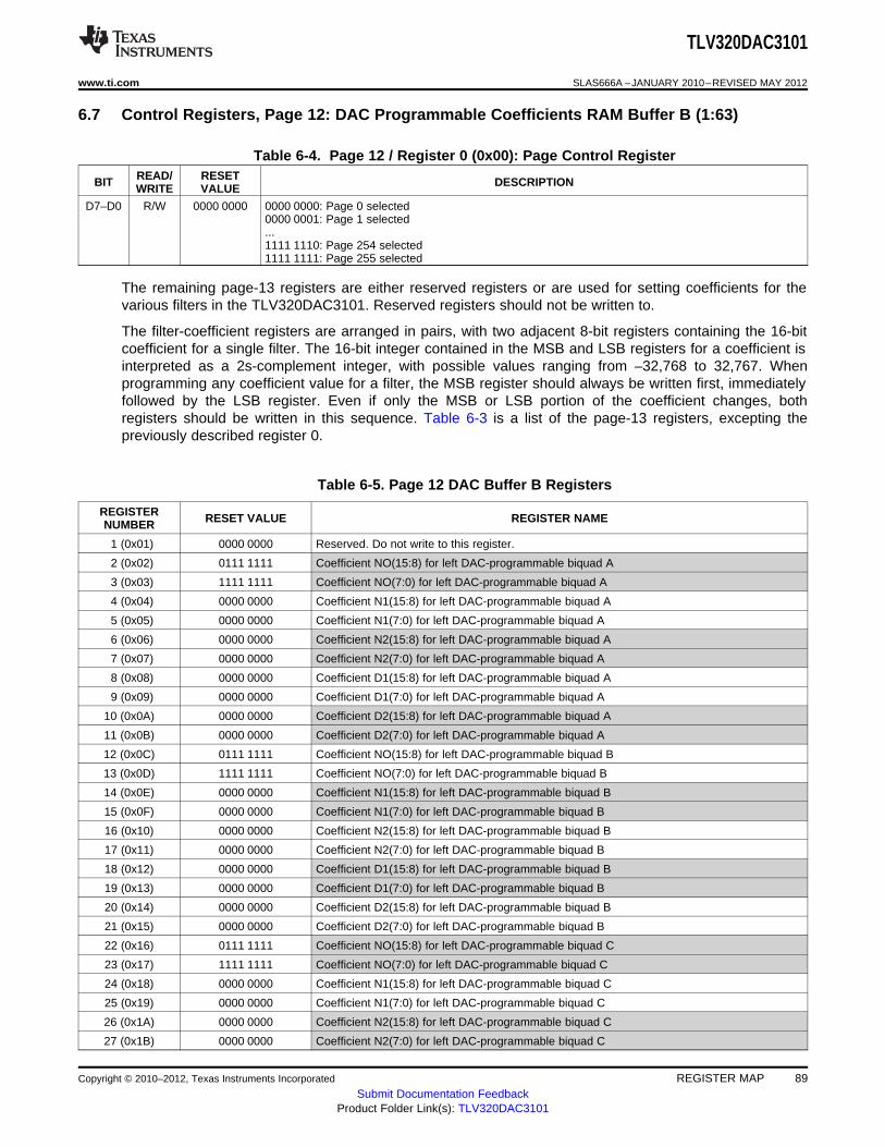
TLV320DAC3101
www.ti.com SLAS666A –JANUARY 2010–REVISED MAY 2012
6.7 Control Registers, Page 12: DAC Programmable Coefficients RAM Buffer B (1:63)
Table 6-4. Page 12 / Register 0 (0x00): Page Control RegisterREAD/ RESETBIT DESCRIPTIONWRITE VALUE
D7–D0 R/W 0000 0000 0000 0000: Page 0 selected0000 0001: Page 1 selected...1111 1110: Page 254 selected1111 1111: Page 255 selected
The remaining page-13 registers are either reserved registers or are used for setting coefficients for thevarious filters in the TLV320DAC3101. Reserved registers should not be written to.
The filter-coefficient registers are arranged in pairs, with two adjacent 8-bit registers containing the 16-bitcoefficient for a single filter. The 16-bit integer contained in the MSB and LSB registers for a coefficient isinterpreted as a 2s-complement integer, with possible values ranging from –32,768 to 32,767. Whenprogramming any coefficient value for a filter, the MSB register should always be written first, immediatelyfollowed by the LSB register. Even if only the MSB or LSB portion of the coefficient changes, bothregisters should be written in this sequence. Table 6-3 is a list of the page-13 registers, excepting thepreviously described register 0.
Table 6-5. Page 12 DAC Buffer B Registers
REGISTER RESET VALUE REGISTER NAMENUMBER
1 (0x01) 0000 0000 Reserved. Do not write to this register.
2 (0x02) 0111 1111 Coefficient NO(15:8) for left DAC-programmable biquad A
3 (0x03) 1111 1111 Coefficient NO(7:0) for left DAC-programmable biquad A
4 (0x04) 0000 0000 Coefficient N1(15:8) for left DAC-programmable biquad A
5 (0x05) 0000 0000 Coefficient N1(7:0) for left DAC-programmable biquad A
6 (0x06) 0000 0000 Coefficient N2(15:8) for left DAC-programmable biquad A
7 (0x07) 0000 0000 Coefficient N2(7:0) for left DAC-programmable biquad A
8 (0x08) 0000 0000 Coefficient D1(15:8) for left DAC-programmable biquad A
9 (0x09) 0000 0000 Coefficient D1(7:0) for left DAC-programmable biquad A
10 (0x0A) 0000 0000 Coefficient D2(15:8) for left DAC-programmable biquad A
11 (0x0B) 0000 0000 Coefficient D2(7:0) for left DAC-programmable biquad A
12 (0x0C) 0111 1111 Coefficient NO(15:8) for left DAC-programmable biquad B
13 (0x0D) 1111 1111 Coefficient NO(7:0) for left DAC-programmable biquad B
14 (0x0E) 0000 0000 Coefficient N1(15:8) for left DAC-programmable biquad B
15 (0x0F) 0000 0000 Coefficient N1(7:0) for left DAC-programmable biquad B
16 (0x10) 0000 0000 Coefficient N2(15:8) for left DAC-programmable biquad B
17 (0x11) 0000 0000 Coefficient N2(7:0) for left DAC-programmable biquad B
18 (0x12) 0000 0000 Coefficient D1(15:8) for left DAC-programmable biquad B
19 (0x13) 0000 0000 Coefficient D1(7:0) for left DAC-programmable biquad B
20 (0x14) 0000 0000 Coefficient D2(15:8) for left DAC-programmable biquad B
21 (0x15) 0000 0000 Coefficient D2(7:0) for left DAC-programmable biquad B
22 (0x16) 0111 1111 Coefficient NO(15:8) for left DAC-programmable biquad C
23 (0x17) 1111 1111 Coefficient NO(7:0) for left DAC-programmable biquad C
24 (0x18) 0000 0000 Coefficient N1(15:8) for left DAC-programmable biquad C
25 (0x19) 0000 0000 Coefficient N1(7:0) for left DAC-programmable biquad C
26 (0x1A) 0000 0000 Coefficient N2(15:8) for left DAC-programmable biquad C
27 (0x1B) 0000 0000 Coefficient N2(7:0) for left DAC-programmable biquad C
Copyright © 2010–2012, Texas Instruments Incorporated REGISTER MAP 89Submit Documentation Feedback
Product Folder Link(s): TLV320DAC3101
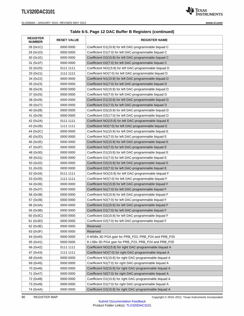
TLV320DAC3101
SLAS666A –JANUARY 2010–REVISED MAY 2012 www.ti.com
Table 6-5. Page 12 DAC Buffer B Registers (continued)
REGISTER RESET VALUE REGISTER NAMENUMBER
28 (0x1C) 0000 0000 Coefficient D1(15:8) for left DAC-programmable biquad C
29 (0x1D) 0000 0000 Coefficient D1(7:0) for left DAC-programmable biquad C
30 (0x1E) 0000 0000 Coefficient D2(15:8) for left DAC-programmable biquad C
31 (0x1F) 0000 0000 Coefficient D2(7:0) for left DAC-programmable biquad C
32 (0x20) 0111 1111 Coefficient NO(15:8) for left DAC-programmable biquad D
33 (0x21) 1111 1111 Coefficient NO(7:0) for left DAC-programmable biquad D
34 (0x22) 0000 0000 Coefficient N1(15:8) for left DAC-programmable biquad D
35 (0x23) 0000 0000 Coefficient N1(7:0) for left DAC-programmable biquad D
36 (0x24) 0000 0000 Coefficient N2(15:8) for left DAC-programmable biquad D
37 (0x25) 0000 0000 Coefficient N2(7:0) for left DAC-programmable biquad D
38 (0x26) 0000 0000 Coefficient D1(15:8) for left DAC-programmable biquad D
39 (0x27) 0000 0000 Coefficient D1(7:0) for left DAC-programmable biquad D
40 (0x28) 0000 0000 Coefficient D2(15:8) for left DAC-programmable biquad D
41 (0x29) 0000 0000 Coefficient D2(17:0) for left DAC-programmable biquad D
42 (0x2A) 0111 1111 Coefficient NO(15:8) for left DAC-programmable biquad E
43 (0x2B) 1111 1111 Coefficient NO(7:0) for left DAC-programmable biquad E
44 (0x2C) 0000 0000 Coefficient N1(15:8) for left DAC-programmable biquad E
45 (0x2D) 0000 0000 Coefficient N1(7:0) for left DAC-programmable biquad E
46 (0x2E) 0000 0000 Coefficient N2(15:8) for left DAC-programmable biquad E
47 (0x2F) 0000 0000 Coefficient N2(7:0) for left DAC-programmable biquad E
48 (0x30) 0000 0000 Coefficient D1(15:8) for left DAC-programmable biquad E
49 (0x31) 0000 0000 Coefficient D1(7:0) for left DAC-programmable biquad E
50 (0x32) 0000 0000 Coefficient D2(15:8) for left DAC-programmable biquad E
51 (0x33) 0000 0000 Coefficient D2(7:0) for left DAC-programmable biquad E
52 (0x34) 0111 1111 Coefficient NO(15:8) for left DAC-programmable biquad F
53 (0x35) 1111 1111 Coefficient NO(7:0) for left DAC-programmable biquad F
54 (0x36) 0000 0000 Coefficient N1(15:8) for left DAC-programmable biquad F
55 (0x37) 0000 0000 Coefficient N1(7:0) for left DAC-programmable biquad F
56 (0x38) 0000 0000 Coefficient N2(15:8) for left DAC-programmable biquad F
57 (0x39) 0000 0000 Coefficient N2(7:0) for left DAC-programmable biquad F
58 (0x3A) 0000 0000 Coefficient D1(15:8) for left DAC-programmable biquad F
59 (0x3B) 0000 0000 Coefficient D1(7:0) for left DAC-programmable biquad F
60 (0x3C) 0000 0000 Coefficient D2(15:8) for left DAC-programmable biquad F
61 (0x3D) 0000 0000 Coefficient D2(7:0) for left DAC-programmable biquad F
62 (0x3E) 0000 0000 Reserved
63 (0x3F) 0000 0000 Reserved
64 (0x40) 0000 0000 8 MSBs 3D PGA gain for PRB_P23, PRB_P24 and PRB_P25
65 (0x41) 0000 0000 8 LSBs 3D PGA gain for PRB_P23, PRB_P24 and PRB_P25
66 (0x42) 0111 1111 Coefficient NO(15:8) for right DAC-programmable biquad A
67 (0x43) 1111 1111 Coefficient NO(7:0) for right DAC-programmable biquad A
68 (0x44) 0000 0000 Coefficient N1(15:8) for right DAC-programmable biquad A
69 (0x45) 0000 0000 Coefficient N1(7:0) for right DAC-programmable biquad A
70 (0x46) 0000 0000 Coefficient N2(15:8) for right DAC-programmable biquad A
71 (0x47) 0000 0000 Coefficient N2(7:0) for right DAC-programmable biquad A
72 (0x48) 0000 0000 Coefficient D1(15:8) for right DAC-programmable biquad A
73 (0x49) 0000 0000 Coefficient D1(7:0) for right DAC-programmable biquad A
74 (0x4A) 0000 0000 Coefficient D2(15:8) for right DAC-programmable biquad A
90 REGISTER MAP Copyright © 2010–2012, Texas Instruments Incorporated
Submit Documentation FeedbackProduct Folder Link(s): TLV320DAC3101
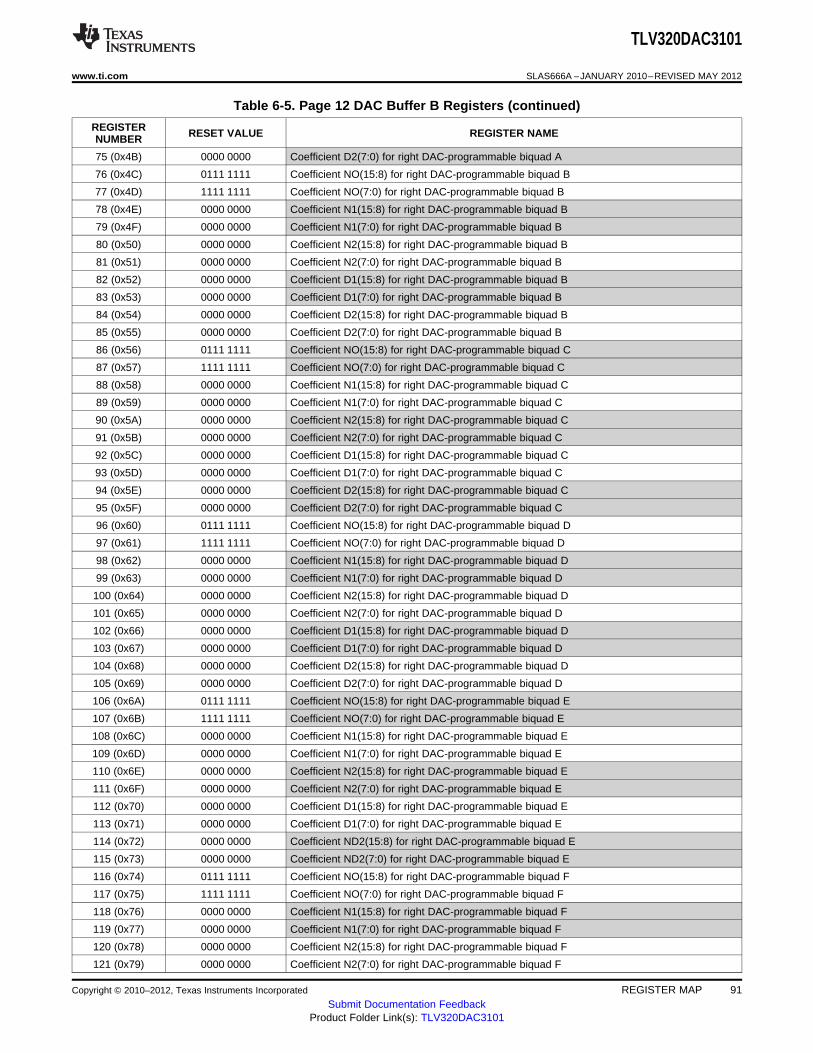
TLV320DAC3101
www.ti.com SLAS666A –JANUARY 2010–REVISED MAY 2012
Table 6-5. Page 12 DAC Buffer B Registers (continued)
REGISTER RESET VALUE REGISTER NAMENUMBER
75 (0x4B) 0000 0000 Coefficient D2(7:0) for right DAC-programmable biquad A
76 (0x4C) 0111 1111 Coefficient NO(15:8) for right DAC-programmable biquad B
77 (0x4D) 1111 1111 Coefficient NO(7:0) for right DAC-programmable biquad B
78 (0x4E) 0000 0000 Coefficient N1(15:8) for right DAC-programmable biquad B
79 (0x4F) 0000 0000 Coefficient N1(7:0) for right DAC-programmable biquad B
80 (0x50) 0000 0000 Coefficient N2(15:8) for right DAC-programmable biquad B
81 (0x51) 0000 0000 Coefficient N2(7:0) for right DAC-programmable biquad B
82 (0x52) 0000 0000 Coefficient D1(15:8) for right DAC-programmable biquad B
83 (0x53) 0000 0000 Coefficient D1(7:0) for right DAC-programmable biquad B
84 (0x54) 0000 0000 Coefficient D2(15:8) for right DAC-programmable biquad B
85 (0x55) 0000 0000 Coefficient D2(7:0) for right DAC-programmable biquad B
86 (0x56) 0111 1111 Coefficient NO(15:8) for right DAC-programmable biquad C
87 (0x57) 1111 1111 Coefficient NO(7:0) for right DAC-programmable biquad C
88 (0x58) 0000 0000 Coefficient N1(15:8) for right DAC-programmable biquad C
89 (0x59) 0000 0000 Coefficient N1(7:0) for right DAC-programmable biquad C
90 (0x5A) 0000 0000 Coefficient N2(15:8) for right DAC-programmable biquad C
91 (0x5B) 0000 0000 Coefficient N2(7:0) for right DAC-programmable biquad C
92 (0x5C) 0000 0000 Coefficient D1(15:8) for right DAC-programmable biquad C
93 (0x5D) 0000 0000 Coefficient D1(7:0) for right DAC-programmable biquad C
94 (0x5E) 0000 0000 Coefficient D2(15:8) for right DAC-programmable biquad C
95 (0x5F) 0000 0000 Coefficient D2(7:0) for right DAC-programmable biquad C
96 (0x60) 0111 1111 Coefficient NO(15:8) for right DAC-programmable biquad D
97 (0x61) 1111 1111 Coefficient NO(7:0) for right DAC-programmable biquad D
98 (0x62) 0000 0000 Coefficient N1(15:8) for right DAC-programmable biquad D
99 (0x63) 0000 0000 Coefficient N1(7:0) for right DAC-programmable biquad D
100 (0x64) 0000 0000 Coefficient N2(15:8) for right DAC-programmable biquad D
101 (0x65) 0000 0000 Coefficient N2(7:0) for right DAC-programmable biquad D
102 (0x66) 0000 0000 Coefficient D1(15:8) for right DAC-programmable biquad D
103 (0x67) 0000 0000 Coefficient D1(7:0) for right DAC-programmable biquad D
104 (0x68) 0000 0000 Coefficient D2(15:8) for right DAC-programmable biquad D
105 (0x69) 0000 0000 Coefficient D2(7:0) for right DAC-programmable biquad D
106 (0x6A) 0111 1111 Coefficient NO(15:8) for right DAC-programmable biquad E
107 (0x6B) 1111 1111 Coefficient NO(7:0) for right DAC-programmable biquad E
108 (0x6C) 0000 0000 Coefficient N1(15:8) for right DAC-programmable biquad E
109 (0x6D) 0000 0000 Coefficient N1(7:0) for right DAC-programmable biquad E
110 (0x6E) 0000 0000 Coefficient N2(15:8) for right DAC-programmable biquad E
111 (0x6F) 0000 0000 Coefficient N2(7:0) for right DAC-programmable biquad E
112 (0x70) 0000 0000 Coefficient D1(15:8) for right DAC-programmable biquad E
113 (0x71) 0000 0000 Coefficient D1(7:0) for right DAC-programmable biquad E
114 (0x72) 0000 0000 Coefficient ND2(15:8) for right DAC-programmable biquad E
115 (0x73) 0000 0000 Coefficient ND2(7:0) for right DAC-programmable biquad E
116 (0x74) 0111 1111 Coefficient NO(15:8) for right DAC-programmable biquad F
117 (0x75) 1111 1111 Coefficient NO(7:0) for right DAC-programmable biquad F
118 (0x76) 0000 0000 Coefficient N1(15:8) for right DAC-programmable biquad F
119 (0x77) 0000 0000 Coefficient N1(7:0) for right DAC-programmable biquad F
120 (0x78) 0000 0000 Coefficient N2(15:8) for right DAC-programmable biquad F
121 (0x79) 0000 0000 Coefficient N2(7:0) for right DAC-programmable biquad F
Copyright © 2010–2012, Texas Instruments Incorporated REGISTER MAP 91Submit Documentation Feedback
Product Folder Link(s): TLV320DAC3101
TLV320DAC3101
SLAS666A –JANUARY 2010–REVISED MAY 2012 www.ti.com
Table 6-5. Page 12 DAC Buffer B Registers (continued)
REGISTER RESET VALUE REGISTER NAMENUMBER
122 (0x7A) 0000 0000 Coefficient D1(15:8) for right DAC-programmable biquad F
123 (0x7B) 0000 0000 Coefficient D1(7:0) for right DAC-programmable biquad F
124 (0x7C) 0000 0000 Coefficient D2(15:8) for right DAC-programmable biquad F
125 (0x7D) 0000 0000 Coefficient D2(7:0) for right DAC-programmable biquad F
126–127 0000 0000 Reserved
6.8 Control Registers, Page 13: DAC Programmable Coefficients RAM Buffer B (65:127)
Table 6-6. Page 13 / Register 0 (0x00): Page Control RegisterREAD/ RESETBIT DESCRIPTIONWRITE VALUE
D7–D0 R/W 0000 0000 0000 0000: Page 0 selected0000 0001: Page 1 selected...1111 1110: Page 254 selected1111 1111: Page 255 selected
Table 6-7. Page 13 DAC Buffer B Registers
REGISTER RESET VALUE REGISTER NAMENUMBER
1 0000 0000 Reserved. Do not write to this register.
2 (0x02) 0111 1111 Coefficient N0(15:8) for left DAC-programmable first-order IIR
3 (0x03) 1111 1111 Coefficient N0(7:0) for left DAC-programmable first-order IIR
4 (0x04) 0000 0000 Coefficient N1(15:8) for left DAC-programmable first-order IIR
5 (0x05) 0000 0000 Coefficient N1(7:0) for left DAC-programmable first-order IIR
6 (0x06) 0000 0000 Coefficient D1(15:8) for left DAC-programmable first-order IIR
7 (0x07) 0000 0000 Coefficient D1(7:0) for left DAC-programmable first-order IIR
8 (0x08) 0111 1111 Coefficient N0(15:8) for right DAC-programmable first-order IIR
9 (0x09) 1111 1111 Coefficient N0(7:0) for right DAC-programmable first-order IIR
10 (0x0A) 0000 0000 Coefficient N1(15:8) for right DAC-programmable first-order IIR
11 (0x0B) 0000 0000 Coefficient N1(7:0) for right DAC-programmable first-order IIR
12 (0x0C) 0000 0000 Coefficient D1(15:8) for right DAC-programmable first-order IIR
13 (0x0D) 0000 0000 Coefficient D1(7:0) for right DAC-programmable first-order IIR
14 (0x0E) 0111 1111 Coefficient N0(15:8) for DRC first-order high-pass filter
15 (0x0F) 1111 0111 Coefficient N0(7:0) for DRC first-order high-pass filter
16 (0x10) 1000 0000 Coefficient N1(15:8) for DRC first-order high-pass filter
17 (0x11) 0000 1001 Coefficient N1(7:0) for DRC first-order high-pass filter
18 (0x12) 0111 1111 Coefficient D1(15:8) for DRC first-order high-pass filter
19 (0x13) 1110 1111 Coefficient D1(7:0) for DRC first-order high-pass filter
20 (0x14) 0000 0000 Coefficient N0(15:8) for DRC first-order low-pass filter
21 (0x15) 0001 0001 Coefficient N0(7:0) for DRC first-order low-pass filter
22 (0x16) 0000 0000 Coefficient N1(15:8) for DRC first-order low-pass filter
23 (0x17) 0001 0001 Coefficient N1(7:0) for DRC first-order low-pass filter
24 (0x18) 0111 1111 Coefficient D1(15:8) for DRC first-order low-pass filter
25 (0x19) 1101 1110 Coefficient D1(7:0) for DRC first-order low-pass filter
26–127 0000 0000 Reserved
92 REGISTER MAP Copyright © 2010–2012, Texas Instruments Incorporated
Submit Documentation FeedbackProduct Folder Link(s): TLV320DAC3101
TLV320DAC3101
www.ti.com SLAS666A –JANUARY 2010–REVISED MAY 2012
Revision HistoryNOTE: Page numbers for previous revisions may differ from page numbers in the current version.
Changes from Original (January, 2010) to Revision A Page
• Changed register 36 to register 35. ........................................................................................... 23• Added D6–D0 to the Register Value column heading and changed Analog Attenuation to Analog Gain. ..... 44• Deleted Analog Volume Control for Headphone and Speaker Outputs (for D7=0) table and added table
note to D7=1 table. ................................................................................................................ 44• Changed page 0 to page 1 in section 5.5.12.1. ............................................................................. 45• Added 80 MHz ≤ (PLL_CLKIN × J.D × R/P) ≤ 110 MHz and 4 ≤ R × J ≤ 259 underneath equation 7. ............. 54• Added 80 MHz ≤ PLL_CLKIN × J.D × R/P ≤ 110 MHz and R = 1 underneath equation 8. ........................... 54• Added Timer section and image after PLL section. ....................................................................... 55• Added table note to Page 0 / Register 64 (0x40): DAC VOLUME CONTROL. ......................................... 73• Changed D0=1 to Reserved in Page 1 / Register 33. ...................................................................... 79• Removed extraneous cross-references for deleted table. ................................................................ 80• Added table note to Page 1 / Register 40 (0x28): HPL Driver. ........................................................... 81• Added table note to Page 1 / Register 41 (0x29): HPR Driver. ........................................................... 81
Copyright © 2010–2012, Texas Instruments Incorporated REGISTER MAP 93Submit Documentation Feedback
Product Folder Link(s): TLV320DAC3101
PACKAGE OPTION ADDENDUM
www.ti.com 27-Jul-2013
Addendum-Page 1
PACKAGING INFORMATION
Orderable Device Status(1)
Package Type PackageDrawing
Pins PackageQty
Eco Plan(2)
Lead/Ball Finish MSL Peak Temp(3)
Op Temp (°C) Device Marking(4/5)
Samples
TLV320DAC3101IRHBR ACTIVE VQFN RHB 32 3000 Green (RoHS& no Sb/Br)
CU NIPDAU Level-2-260C-1 YEAR -40 to 85 DAC3101
TLV320DAC3101IRHBT ACTIVE VQFN RHB 32 250 Green (RoHS& no Sb/Br)
CU NIPDAU Level-2-260C-1 YEAR -40 to 85 DAC3101
(1) The marketing status values are defined as follows:ACTIVE: Product device recommended for new designs.LIFEBUY: TI has announced that the device will be discontinued, and a lifetime-buy period is in effect.NRND: Not recommended for new designs. Device is in production to support existing customers, but TI does not recommend using this part in a new design.PREVIEW: Device has been announced but is not in production. Samples may or may not be available.OBSOLETE: TI has discontinued the production of the device.
(2) Eco Plan - The planned eco-friendly classification: Pb-Free (RoHS), Pb-Free (RoHS Exempt), or Green (RoHS & no Sb/Br) - please check http://www.ti.com/productcontent for the latest availabilityinformation and additional product content details.TBD: The Pb-Free/Green conversion plan has not been defined.Pb-Free (RoHS): TI's terms "Lead-Free" or "Pb-Free" mean semiconductor products that are compatible with the current RoHS requirements for all 6 substances, including the requirement thatlead not exceed 0.1% by weight in homogeneous materials. Where designed to be soldered at high temperatures, TI Pb-Free products are suitable for use in specified lead-free processes.Pb-Free (RoHS Exempt): This component has a RoHS exemption for either 1) lead-based flip-chip solder bumps used between the die and package, or 2) lead-based die adhesive used betweenthe die and leadframe. The component is otherwise considered Pb-Free (RoHS compatible) as defined above.Green (RoHS & no Sb/Br): TI defines "Green" to mean Pb-Free (RoHS compatible), and free of Bromine (Br) and Antimony (Sb) based flame retardants (Br or Sb do not exceed 0.1% by weightin homogeneous material)
(3) MSL, Peak Temp. -- The Moisture Sensitivity Level rating according to the JEDEC industry standard classifications, and peak solder temperature.
(4) There may be additional marking, which relates to the logo, the lot trace code information, or the environmental category on the device.
(5) Multiple Device Markings will be inside parentheses. Only one Device Marking contained in parentheses and separated by a "~" will appear on a device. If a line is indented then it is a continuationof the previous line and the two combined represent the entire Device Marking for that device.
Important Information and Disclaimer:The information provided on this page represents TI's knowledge and belief as of the date that it is provided. TI bases its knowledge and belief on informationprovided by third parties, and makes no representation or warranty as to the accuracy of such information. Efforts are underway to better integrate information from third parties. TI has taken andcontinues to take reasonable steps to provide representative and accurate information but may not have conducted destructive testing or chemical analysis on incoming materials and chemicals.TI and TI suppliers consider certain information to be proprietary, and thus CAS numbers and other limited information may not be available for release.
In no event shall TI's liability arising out of such information exceed the total purchase price of the TI part(s) at issue in this document sold by TI to Customer on an annual basis.
TAPE AND REEL INFORMATION
*All dimensions are nominal
Device PackageType
PackageDrawing
Pins SPQ ReelDiameter
(mm)
ReelWidth
W1 (mm)
A0(mm)
B0(mm)
K0(mm)
P1(mm)
W(mm)
Pin1Quadrant
TLV320DAC3101IRHBR VQFN RHB 32 3000 330.0 12.4 5.3 5.3 1.1 8.0 12.0 Q2
TLV320DAC3101IRHBR VQFN RHB 32 3000 330.0 12.4 5.3 5.3 1.5 8.0 12.0 Q2
TLV320DAC3101IRHBT VQFN RHB 32 250 180.0 12.4 5.3 5.3 1.1 8.0 12.0 Q2
TLV320DAC3101IRHBT VQFN RHB 32 250 180.0 12.4 5.3 5.3 1.5 8.0 12.0 Q2
PACKAGE MATERIALS INFORMATION
www.ti.com 18-Aug-2014
Pack Materials-Page 1
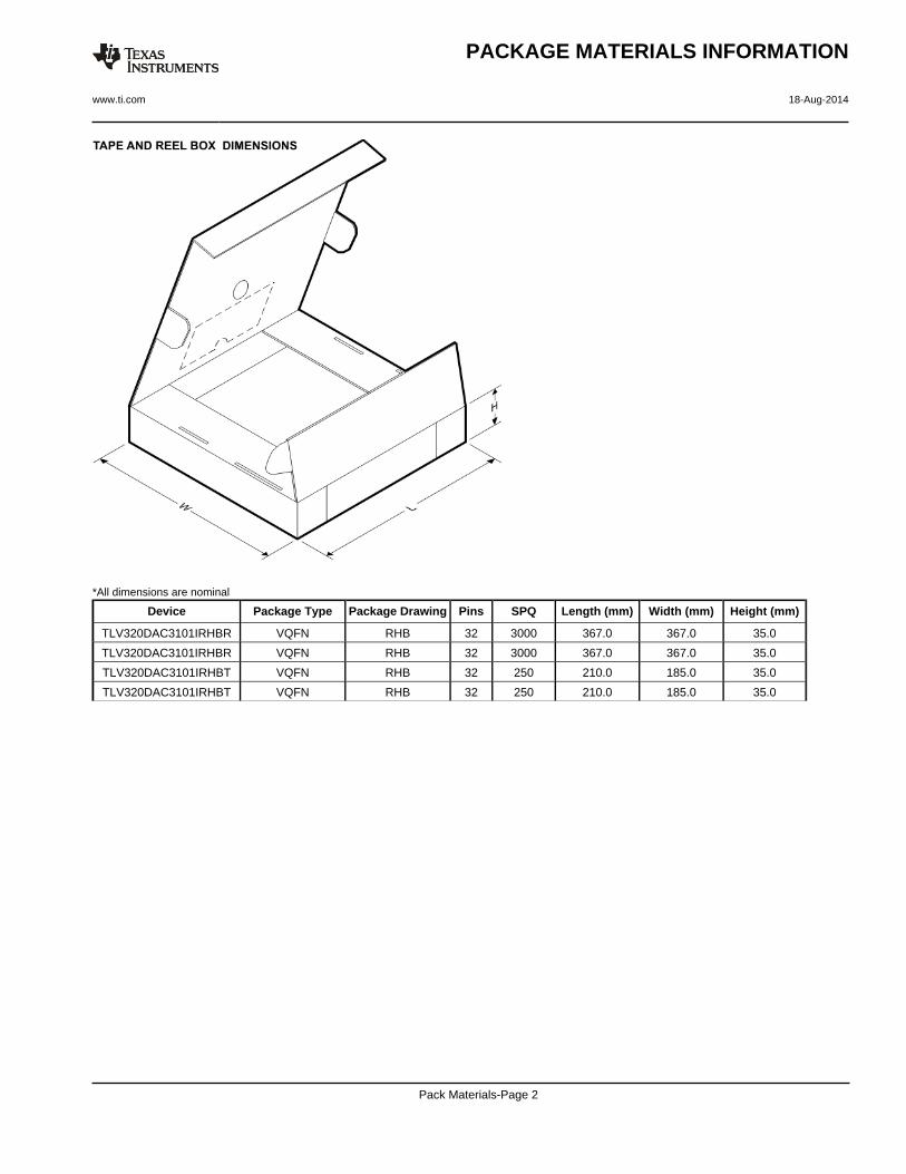
*All dimensions are nominal
Device Package Type Package Drawing Pins SPQ Length (mm) Width (mm) Height (mm)
TLV320DAC3101IRHBR VQFN RHB 32 3000 367.0 367.0 35.0
TLV320DAC3101IRHBR VQFN RHB 32 3000 367.0 367.0 35.0
TLV320DAC3101IRHBT VQFN RHB 32 250 210.0 185.0 35.0
TLV320DAC3101IRHBT VQFN RHB 32 250 210.0 185.0 35.0
PACKAGE MATERIALS INFORMATION
www.ti.com 18-Aug-2014
Pack Materials-Page 2
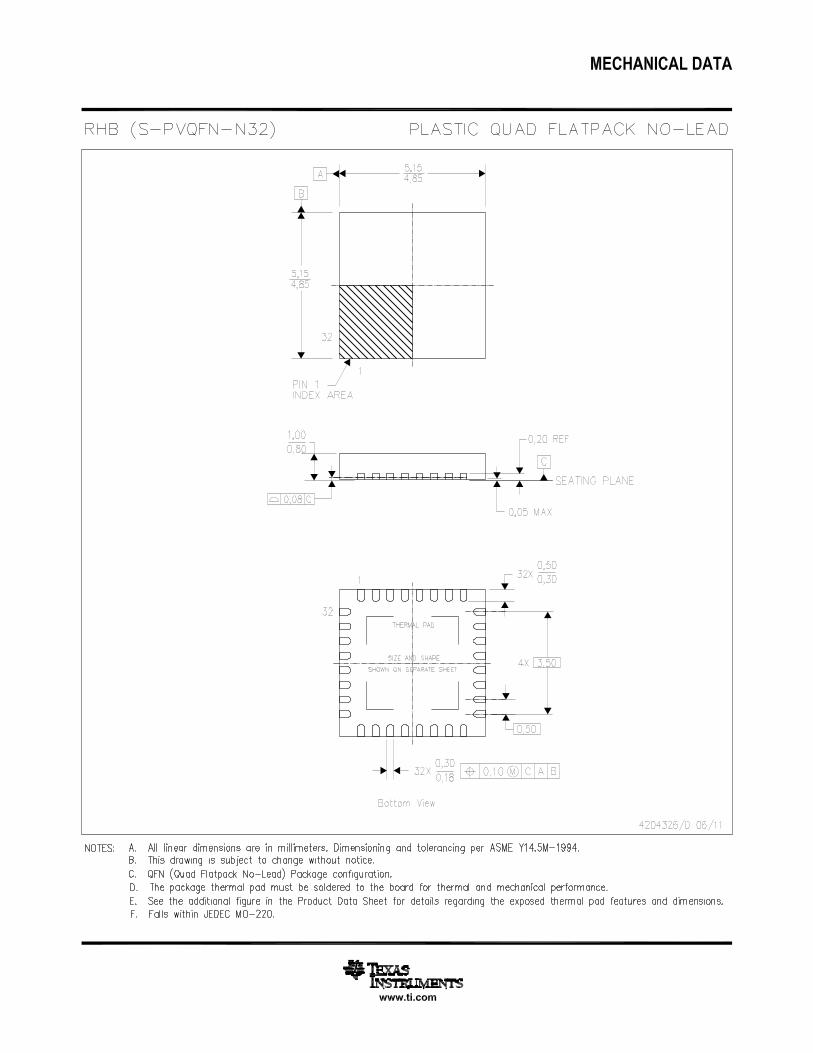
IMPORTANT NOTICE
Texas Instruments Incorporated and its subsidiaries (TI) reserve the right to make corrections, enhancements, improvements and otherchanges to its semiconductor products and services per JESD46, latest issue, and to discontinue any product or service per JESD48, latestissue. Buyers should obtain the latest relevant information before placing orders and should verify that such information is current andcomplete. All semiconductor products (also referred to herein as “components”) are sold subject to TI’s terms and conditions of salesupplied at the time of order acknowledgment.TI warrants performance of its components to the specifications applicable at the time of sale, in accordance with the warranty in TI’s termsand conditions of sale of semiconductor products. Testing and other quality control techniques are used to the extent TI deems necessaryto support this warranty. Except where mandated by applicable law, testing of all parameters of each component is not necessarilyperformed.TI assumes no liability for applications assistance or the design of Buyers’ products. Buyers are responsible for their products andapplications using TI components. To minimize the risks associated with Buyers’ products and applications, Buyers should provideadequate design and operating safeguards.TI does not warrant or represent that any license, either express or implied, is granted under any patent right, copyright, mask work right, orother intellectual property right relating to any combination, machine, or process in which TI components or services are used. Informationpublished by TI regarding third-party products or services does not constitute a license to use such products or services or a warranty orendorsement thereof. Use of such information may require a license from a third party under the patents or other intellectual property of thethird party, or a license from TI under the patents or other intellectual property of TI.Reproduction of significant portions of TI information in TI data books or data sheets is permissible only if reproduction is without alterationand is accompanied by all associated warranties, conditions, limitations, and notices. TI is not responsible or liable for such altereddocumentation. Information of third parties may be subject to additional restrictions.Resale of TI components or services with statements different from or beyond the parameters stated by TI for that component or servicevoids all express and any implied warranties for the associated TI component or service and is an unfair and deceptive business practice.TI is not responsible or liable for any such statements.Buyer acknowledges and agrees that it is solely responsible for compliance with all legal, regulatory and safety-related requirementsconcerning its products, and any use of TI components in its applications, notwithstanding any applications-related information or supportthat may be provided by TI. Buyer represents and agrees that it has all the necessary expertise to create and implement safeguards whichanticipate dangerous consequences of failures, monitor failures and their consequences, lessen the likelihood of failures that might causeharm and take appropriate remedial actions. Buyer will fully indemnify TI and its representatives against any damages arising out of the useof any TI components in safety-critical applications.In some cases, TI components may be promoted specifically to facilitate safety-related applications. With such components, TI’s goal is tohelp enable customers to design and create their own end-product solutions that meet applicable functional safety standards andrequirements. Nonetheless, such components are subject to these terms.No TI components are authorized for use in FDA Class III (or similar life-critical medical equipment) unless authorized officers of the partieshave executed a special agreement specifically governing such use.Only those TI components which TI has specifically designated as military grade or “enhanced plastic” are designed and intended for use inmilitary/aerospace applications or environments. Buyer acknowledges and agrees that any military or aerospace use of TI componentswhich have not been so designated is solely at the Buyer's risk, and that Buyer is solely responsible for compliance with all legal andregulatory requirements in connection with such use.TI has specifically designated certain components as meeting ISO/TS16949 requirements, mainly for automotive use. In any case of use ofnon-designated products, TI will not be responsible for any failure to meet ISO/TS16949.
Products ApplicationsAudio www.ti.com/audio Automotive and Transportation www.ti.com/automotiveAmplifiers amplifier.ti.com Communications and Telecom www.ti.com/communicationsData Converters dataconverter.ti.com Computers and Peripherals www.ti.com/computersDLP® Products www.dlp.com Consumer Electronics www.ti.com/consumer-appsDSP dsp.ti.com Energy and Lighting www.ti.com/energyClocks and Timers www.ti.com/clocks Industrial www.ti.com/industrialInterface interface.ti.com Medical www.ti.com/medicalLogic logic.ti.com Security www.ti.com/securityPower Mgmt power.ti.com Space, Avionics and Defense www.ti.com/space-avionics-defenseMicrocontrollers microcontroller.ti.com Video and Imaging www.ti.com/videoRFID www.ti-rfid.comOMAP Applications Processors www.ti.com/omap TI E2E Community e2e.ti.comWireless Connectivity www.ti.com/wirelessconnectivity
Mailing Address: Texas Instruments, Post Office Box 655303, Dallas, Texas 75265Copyright © 2016, Texas Instruments Incorporated