Embed Size (px)
Citation preview
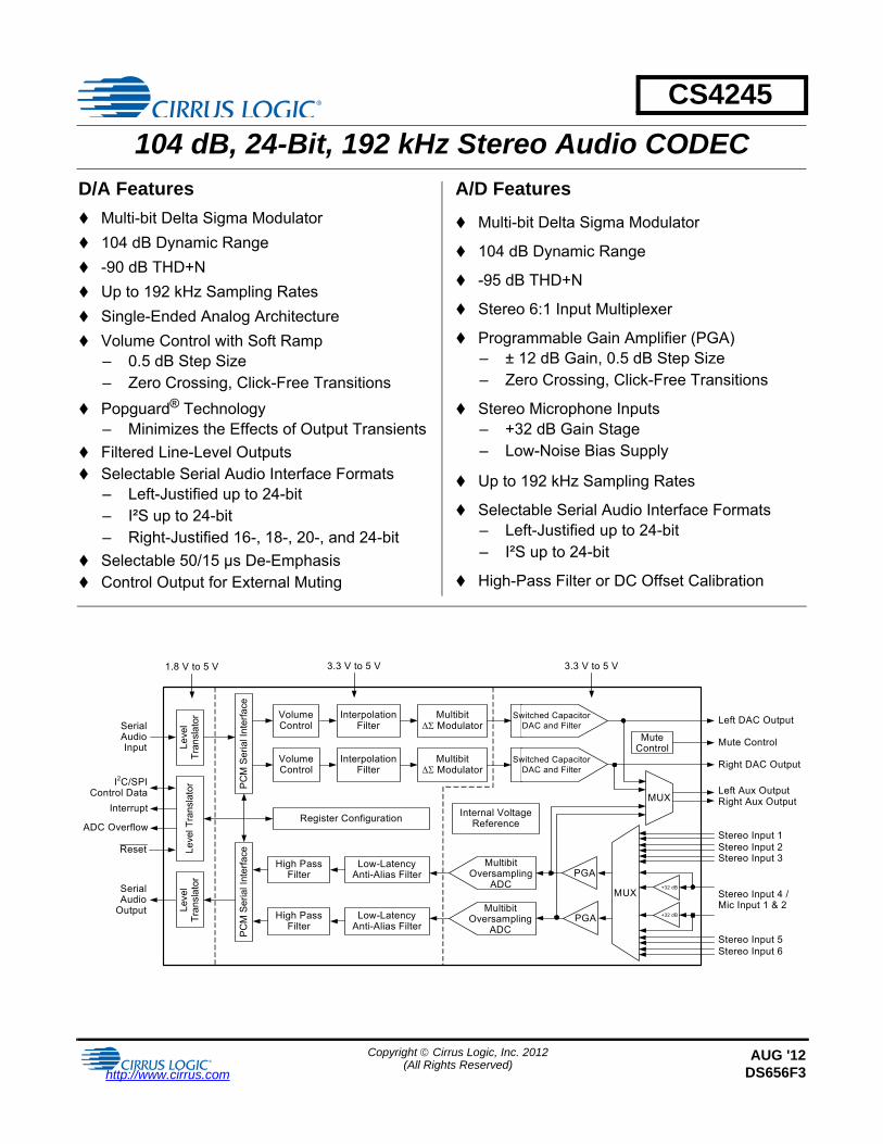
CS4245
104 dB, 24-Bit, 192 kHz Stereo Audio CODEC
D/A Features
Multi-bit Delta Sigma Modulator 104 dB Dynamic Range -90 dB THD+N Up to 192 kHz Sampling Rates Single-Ended Analog Architecture Volume Control with Soft Ramp
– 0.5 dB Step Size– Zero Crossing, Click-Free Transitions
Popguard® Technology– Minimizes the Effects of Output Transients
Filtered Line-Level Outputs Selectable Serial Audio Interface Formats
– Left-Justified up to 24-bit– I²S up to 24-bit– Right-Justified 16-, 18-, 20-, and 24-bit
Selectable 50/15 µs De-Emphasis Control Output for External Muting
A/D Features
Multi-bit Delta Sigma Modulator
104 dB Dynamic Range
-95 dB THD+N
Stereo 6:1 Input Multiplexer
Programmable Gain Amplifier (PGA)– ± 12 dB Gain, 0.5 dB Step Size– Zero Crossing, Click-Free Transitions
Stereo Microphone Inputs– +32 dB Gain Stage– Low-Noise Bias Supply
Up to 192 kHz Sampling Rates
Selectable Serial Audio Interface Formats– Left-Justified up to 24-bit– I²S up to 24-bit
High-Pass Filter or DC Offset Calibration
1.8 V to 5 V
MultibitModulator
MultibitModulator
Low-LatencyAnti-Alias Filter
Internal Voltage Reference
InterpolationFilter
InterpolationFilter
Left DAC Output
Right DAC OutputSwitched Capacitor DAC and Filter
MultibitOversampling
ADC
MultibitOversampling
ADCLow-Latency
Anti-Alias Filter
High Pass Filter
High Pass Filter
Stereo Input 1
Serial Audio Input
Serial Audio
Output
3.3 V to 5 V 3.3 V to 5 V
Switched Capacitor DAC and Filter
MUX
PGA
MUX
Volume Control
Volume Control
PC
M S
eria
l Int
erfa
ceP
CM
Ser
ial I
nter
face
Mute Control
Register Configuration
Leve
l Tr
ansl
ator
Leve
l Tra
nsla
tor
Leve
l Tr
ansl
ator
Reset
I2C/SPIControl Data
Mute Control
Left Aux OutputRight Aux Output
Stereo Input 2Stereo Input 3
Stereo Input 4 / Mic Input 1 & 2
Stereo Input 5Stereo Input 6
PGA+32 dB
+32 dB
Interrupt
ADC Overflow
Copyright Cirrus Logic, Inc. 2012(All Rights Reserved)
http://www.cirrus.com
AUG '12DS656F3
CS4245
System Features
Direct Interface with 1.8 V to 5 V Logic Levels
Optional Asynchronous Serial Port Operation– Each Serial Port Supports Master or Slave
Operation
Selectable Auxiliary Analog Output– Allows Analog Monitoring of Either the ADC
Input Signal after PGA or DAC Output Signal
Internal Digital Loopback
Power-Down Mode– Available for A/D, D/A, CODEC, Mic
Preamplifier
+3.3 V to +5 V Analog Power Supply
+3.3 V to +5 V Digital Power Supply
Supports I²C® and SPITM Control Port Interfaces
Pin-Compatible with CS5345
General Description
The CS4245 is a h ighly integrated stereo audioCODEC. The CS4245 performs stereo analog-to-digital(A/D) and digital-to-analog (D/A) conversion of up to24-bit serial values at sample rates up to 192 kHz.
A 6:1 stereo input multiplexer is included for s electingbetween line-level or microphone-level inputs. The mi-crophone input path includes a +32 dB gain stage anda low-noise bias voltage supply. The PGA is availablefor line or microphone inputs and provides gain/attenu-ation of 12 dB in 0.5 dB steps.
The output of the PGA is followed by an advanced 5th-order, multi-bit delta sigma modulator and digital filter-ing/decimation. Sampled data is transmitted by theserial audio interface at rates from 4 kHz to 192 kHz ineither Slave or Master Mode.
The D/A converter is based on a 4th-order multi-bit deltasigma modulator with an ultra-linear low-pass filter andoffers a volume control that operates with a 0.5 dB stepsize. It in corporates selectable soft ramp and zerocrossing transition functions to eliminate clicks andpops.
Standard 50/15 s de-emphasis is availa ble for a44.1 kHz sample rate for compatibility with digital audioprograms mastered using the 50 /15 s pre-emphasistechnique.
Integrated level translators allow ea sy interfacing be-tween the CS4245 and other devices operating over awide range of logic levels.
The CS4245 is available in a 48-pin LQFP package inboth Commercial (-10° to +70° C) and Automotive (-40°to +105° C) grade. The CDB4245 Customer Demon-stration board is also available for device evaluation andimplementation suggestions. Please see “Ordering In-formation” on page 58 for complete details.
2 DS656F3
CS4245
TABLE OF CONTENTS1. PIN DESCRIPTIONS ........................................................................................................................ 72. CHARACTERISTICS AND SPECIFICATIONS ...................................................................................... 9
SPECIFIED OPERATING CONDITIONS ............................................................................................. 9ABSOLUTE MAXIMUM RATINGS ....................................................................................................... 9DAC ANALOG CHARACTERISTICS ................................................................................................. 10DAC COMBINED INTERPOLATION & ON-CHIP ANALOG FILTER RESPONSE ............................ 11ADC ANALOG CHARACTERISTICS ................................................................................................. 13ADC ANALOG CHARACTERISTICS ................................................................................................. 15ADC DIGITAL FILTER CHARACTERISTICS ..................................................................................... 16AUXILIARY OUTPUT ANALOG CHARACTERISTICS ...................................................................... 17AUXILIARY OUTPUT ANALOG CHARACTERISTICS ...................................................................... 18AUXILIARY OUTPUT ANALOG CHARACTERISTICS ...................................................................... 19DC ELECTRICAL CHARACTERISTICS ............................................................................................. 20DIGITAL INTERFACE CHARACTERISTICS ...................................................................................... 21SWITCHING CHARACTERISTICS - SERIAL AUDIO PORT 1 .......................................................... 22SWITCHING CHARACTERISTICS - SERIAL AUDIO PORT 2 .......................................................... 24SWITCHING CHARACTERISTICS - CONTROL PORT - I²C FORMAT ............................................ 27SWITCHING CHARACTERISTICS - CONTROL PORT - SPI FORMAT ........................................... 28
3. TYPICAL CONNECTION DIAGRAM ................................................................................................... 294. APPLICATIONS ................................................................................................................................... 30
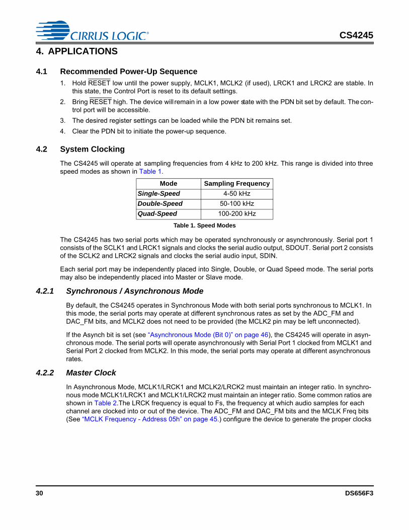
4.1 Recommended Power-Up Sequence ............................................................................................. 304.2 System Clocking ............................................................................................................................. 30
4.2.1 Synchronous / Asynchronous Mode ...................................................................................... 304.2.2 Master Clock ......................................................................................................................... 304.2.3 Master Mode ......................................................................................................................... 324.2.4 Slave Mode ........................................................................................................................... 32
4.3 High-Pass Filter and DC Offset Calibration .................................................................................... 324.4 Analog Input Multiplexer, PGA, and Mic Gain ................................................................................ 344.5 Input Connections ........................................................................................................................... 344.6 Output Connections ........................................................................................................................ 344.7 Output Transient Control ................................................................................................................ 35
4.7.1 Power-Up .............................................................................................................................. 354.7.2 Power-Down .......................................................................................................................... 354.7.3 Serial Interface Clock Changes ............................................................................................. 35
4.8 Auxiliary Analog Output .................................................................................................................. 354.9 De-Emphasis Filter ......................................................................................................................... 354.10 Internal Digital Loopback .............................................................................................................. 364.11 Mute Control ................................................................................................................................. 364.12 Control Port Description and Timing ............................................................................................. 37
4.12.1 SPI Mode ............................................................................................................................. 374.12.2 I²C Mode .............................................................................................................................. 38
4.13 Interrupts and Overflow ................................................................................................................ 394.14 Reset ............................................................................................................................................ 404.15 Synchronization of Multiple Devices ............................................................................................. 404.16 Grounding and Power Supply Decoupling .................................................................................... 40
5. REGISTER QUICK REFERENCE ........................................................................................................ 416. REGISTER DESCRIPTION .................................................................................................................. 42
6.1 Chip ID - Register 01h .................................................................................................................... 426.2 Power Control - Address 02h ......................................................................................................... 42
6.2.1 Freeze (Bit 7) ......................................................................................................................... 426.2.2 Power-Down MIC (Bit 3) ........................................................................................................ 426.2.3 Power-Down ADC (Bit 2) ....................................................................................................... 42
DS656F3 3
CS4245
6.2.4 Power-Down DAC (Bit 1) ....................................................................................................... 436.2.5 Power-Down Device (Bit 0) ................................................................................................... 43
6.3 DAC Control - Address 03h ............................................................................................................ 436.3.1 DAC Functional Mode (Bits 7:6) ............................................................................................ 436.3.2 DAC Digital Interface Format (Bits 5:4) ................................................................................. 436.3.3 Mute DAC (Bit 2) ................................................................................................................... 436.3.4 De-Emphasis Control (Bit 1) .................................................................................................. 446.3.5 DAC Master / Slave Mode (Bit 0) .......................................................................................... 44
6.4 ADC Control - Address 04h ............................................................................................................ 446.4.1 ADC Functional Mode (Bits 7:6) ............................................................................................ 446.4.2 ADC Digital Interface Format (Bit 4) ...................................................................................... 456.4.3 Mute ADC (Bit 2) ................................................................................................................... 456.4.4 ADC High-Pass Filter Freeze (Bit 1) ..................................................................................... 456.4.5 ADC Master / Slave Mode (Bit 0) .......................................................................................... 45
6.5 MCLK Frequency - Address 05h .................................................................................................... 456.5.1 Master Clock 1 Frequency (Bits 6:4) ..................................................................................... 456.5.2 Master Clock 2 Frequency (Bits 2:0) ..................................................................................... 46
6.6 Signal Selection - Address 06h ...................................................................................................... 466.6.1 Auxiliary Output Source Select (Bits 6:5) .............................................................................. 466.6.2 Digital Loopback (Bit 1) ......................................................................................................... 466.6.3 Asynchronous Mode (Bit 0) ................................................................................................... 46
6.7 Channel B PGA Control - Address 07h .......................................................................................... 476.7.1 Channel B PGA Gain (Bits 5:0) ............................................................................................. 47
6.8 Channel A PGA Control - Address 08h .......................................................................................... 476.8.1 Channel A PGA Gain (Bits 5:0) ............................................................................................. 47
6.9 ADC Input Control - Address 09h ................................................................................................... 476.9.1 PGA Soft Ramp or Zero Cross Enable (Bits 4:3) .................................................................. 476.9.2 Analog Input Selection (Bits 2:0) ........................................................................................... 48
6.10 DAC Channel A Volume Control - Address 0Ah ........................................................................... 486.11 DAC Channel B Volume Control - Address 0Bh ........................................................................... 48
6.11.1 Volume Control (Bits 7:0) .................................................................................................... 486.12 DAC Control 2 - Address 0Ch ...................................................................................................... 49
6.12.1 DAC Soft Ramp or Zero Cross Enable (Bits 7:6) ................................................................ 496.12.2 Invert DAC Output (Bit 5) .................................................................................................... 496.12.3 Active High/Low (Bit 0) ........................................................................................................ 50
6.13 Interrupt Status - Address 0Dh ..................................................................................................... 506.13.1 ADC Clock Error (Bit 3) ....................................................................................................... 506.13.2 DAC Clock Error (Bit 2) ....................................................................................................... 506.13.3 ADC Overflow (Bit 1) ........................................................................................................... 506.13.4 ADC Underflow (Bit 0) ......................................................................................................... 50
6.14 Interrupt Mask - Address 0Eh ....................................................................................................... 506.15 Interrupt Mode MSB - Address 0Fh .............................................................................................. 516.16 Interrupt Mode LSB - Address 10h ............................................................................................... 51
7. PARAMETER DEFINITIONS ................................................................................................................ 528. DAC FILTER PLOTS .................................................................................................................... 539. ADC FILTER PLOTS ......................................................................................................................... 5510. PACKAGE DIMENSIONS .................................................................................................................. 5711. THERMAL CHARACTERISTICS AND SPECIFICATIONS ............................................................. 5712. ORDERING INFORMATION ..................................................................................................... 5813. REVISION HISTORY .......................................................................................................................... 58
4 DS656F3
CS4245
LIST OF FIGURESFigure 1.DAC Output Test Load ................................................................................................................ 12Figure 2.Maximum DAC Loading .............................................................................................................. 12Figure 3.Master Mode Timing - Serial Audio Port 1 .................................................................................. 23Figure 4.Slave Mode Timing - Serial Audio Port 1 .................................................................................... 23Figure 5.Master Mode Timing - Serial Audio Port 2 .................................................................................. 25Figure 6.Slave Mode Timing - Serial Audio Port 2 .................................................................................... 25Figure 7.Format 0, Left-Justified up to 24-Bit Data ................................................................................... 26Figure 8.Format 1, I²S up to 24-Bit Data ................................................................................................... 26Figure 9.Format 2, Right-Justified 16-Bit Data.Format 3, Right-Justified 24-Bit Data. ....................................................................................................... 26Figure 10.Control Port Timing - I²C Format ............................................................................................... 27Figure 11.Control Port Timing - SPI Format .............................................................................................. 28Figure 12.Typical Connection Diagram ..................................................................................................... 29Figure 13.Master Mode Clocking .............................................................................................................. 32Figure 14.Analog Input Architecture .......................................................................................................... 34Figure 15.De-Emphasis Curve .................................................................................................................. 36Figure 16.Suggested Active-Low Mute Circuit .......................................................................................... 37Figure 17.Control Port Timing in SPI Mode .............................................................................................. 38Figure 18.Control Port Timing, I²C Write ................................................................................................... 38Figure 19.Control Port Timing, I²C Read ................................................................................................... 39Figure 20.De-Emphasis Curve .................................................................................................................. 44Figure 21.DAC Single-Speed Stopband Rejection ................................................................................... 53Figure 22.DAC Single-Speed Transition Band .......................................................................................... 53Figure 23.DAC Single-Speed Transition Band .......................................................................................... 53Figure 24.DAC Single-Speed Passband Ripple ........................................................................................ 53Figure 25.DAC Double-Speed Stopband Rejection .................................................................................. 53Figure 26.DAC Double-Speed Transition Band ........................................................................................ 53Figure 27.DAC Double-Speed Transition Band ........................................................................................ 54Figure 28.DAC Double-Speed Passband Ripple ...................................................................................... 54Figure 29.DAC Quad-Speed Stopband Rejection ..................................................................................... 54Figure 30.DAC Quad-Speed Transition Band ........................................................................................... 54Figure 31.DAC Quad-Speed Transition Band ........................................................................................... 54Figure 32.DAC Quad-Speed Passband Ripple ......................................................................................... 54Figure 33.ADC Single-Speed Stopband Rejection ................................................................................... 55Figure 34.ADC Single-Speed Stopband Rejection ................................................................................... 55Figure 35.ADC Single-Speed Transition Band (Detail) ............................................................................. 55Figure 36.ADC Single-Speed Passband Ripple ........................................................................................ 55Figure 37.ADC Double-Speed Stopband Rejection .................................................................................. 55Figure 38.ADC Double-Speed Stopband Rejection .................................................................................. 55Figure 39.ADC Double-Speed Transition Band (Detail) ............................................................................ 56Figure 40.ADC Double-Speed Passband Ripple ...................................................................................... 56Figure 41.ADC Quad-Speed Stopband Rejection ..................................................................................... 56Figure 42.ADC Quad-Speed Stopband Rejection ..................................................................................... 56Figure 43.ADC Quad-Speed Transition Band (Detail) .............................................................................. 56Figure 44.ADC Quad-Speed Passband Ripple ......................................................................................... 56
LIST OF TABLESTable 1. Speed Modes .............................................................................................................................. 30Table 2. Common Clock Frequencies ....................................................................................................... 31Table 3. Slave Mode MCLK Dividers ........................................................................................................ 31Table 4. Slave Mode Serial Bit Clock Ratios ............................................................................................. 32Table 5. Device Revision .......................................................................................................................... 42
DS656F3 5
CS4245
Table 6. Freeze-able Bits .......................................................................................................................... 42Table 7. Functional Mode Selection ......................................................................................................... 43Table 8. DAC Digital Interface Formats .................................................................................................... 43Table 9. De-Emphasis Control .................................................................................................................. 44Table 10. Functional Mode Selection ........................................................................................................ 44Table 11. ADC Digital Interface Formats .................................................................................................. 45Table 12. MCLK 1 Frequency ................................................................................................................... 45Table 13. MCLK 2 Frequency ................................................................................................................... 46Table 14. Auxiliary Output Source Selection ............................................................................................. 46Table 15. Example Gain and Attenuation Settings ................................................................................... 47Table 16. PGA Soft Cross or Zero Cross Mode Selection ........................................................................ 48Table 17. Analog Input Multiplexer Selection ............................................................................................ 48Table 18. Digital Volume Control Example Settings ................................................................................. 49Table 19. DAC Soft Cross or Zero Cross Mode Selection ........................................................................ 49
6 DS656F3
CS4245
1. PIN DESCRIPTIONS
Pin Name # Pin Description
SDA/CDOUT 1 Serial Control Data (Input/Output) - SDA is a data I/O in I²C Mode. CDOUT is the output data line for the control port interface in SPI Mode.
SCL/CCLK 2 Serial Control Port Clock (Input) - Serial clock for the serial control port.
AD0/CS 3 Address Bit 0 (I²C) / Control Port Chip Select (SPI) (Input) - AD0 is a chip address pin in I²C Mode; CS is the chip-select signal for SPI format.
AD1/CDIN 4 Address Bit 1 (I²C) / Serial Control Data Input (SPI) (Input) - AD1 is a chip address pin in I²C Mode; CDIN is the input data line for the control port interface in SPI Mode.
VLC 5 Control Port Power (Input) - Determines the required signal level for the control port interface. Refer to the Recommended Operating Conditions for appropriate voltages.
RESET 6 Reset (Input) - The device enters a low power mode when this pin is driven low.
AIN3AAIN3B 7, 8 Stereo Analog Input 3 (Input) - The full-scale level is specified in the ADC Analog Characteristics
specification table.
AIN2AAIN2B 9, 10 Stereo Analog Input 2 (Input) - The full-scale level is specified in the ADC Analog Characteristics
specification table.
AIN1AAIN1B 11, 12 Stereo Analog Input 1 (Input) - The full-scale level is specified in the ADC Analog Characteristics
specification table.
1
2
3
4
5
6
7
8
9
10
11
12
13 14 15 16 17 18 19 20 21 22 23 24
48 47 46 45 44 43 42 41 40 39 38 37
36
35
34
33
32
31
30
29
28
27
26
25
VLSSDA/CDOUT
AG
ND
OV
FLSCL/CCLK
AD0/CS
AD1/CDIN
VLC
RESET
AIN3A
AIN3B
AIN2A
AIN2B
AIN1A
AIN1B
VA
AFI
LTB
VQ
1
VQ
2
FILT
1+
FILT
2+
AIN
4A/M
ICIN
1
AIN
4B/M
ICIN
2
AIN
5A
AIN
5B
AFI
LTA
MUTEC
AOUTB
AOUTA
AGND
AGND
VA
AUXOUTB
AUXOUTA
AIN6B
AIN6A
MICBIAS
INT
VD
DG
ND
MC
LK1
LRC
K1
SC
LK1
SD
OU
T
MC
LK2
LRC
K2
SC
LK2
SD
IN
CS4245
DS656F3 7
CS4245
AGND 13 Analog Ground (Input) - Ground reference for the internal analog section.
VA 14 Analog Power (Input) - Positive power for the internal analog section.
AFILTA 15 Antialias Filter Connection (Output) - Antialias filter connection for the channel A ADC input.
AFILTB 16 Antialias Filter Connection (Output) - Antialias filter connection for the channel B ADC input.
VQ1 17 Quiescent Voltage 1 (Output) - Filter connection for the internal quiescent reference voltage.
VQ2 18 Quiescent Voltage 2 (Output) - Filter connection for the internal quiescent reference voltage.
FILT1+ 19 Positive Voltage Reference 1 (Output) - Positive reference voltage for the internal sampling circuits.
FILT2+ 20 Positive Voltage Reference 2 (Output) - Positive reference voltage for the internal sampling circuits.
AIN4A/MICIN1AIN4B/MICIN2 21, 22 Stereo Analog Input 4 / Microphone Input 1 & 2 (Input) - The full-scale level is specified in the ADC
Analog Characteristics specification table.
AIN5AAIN5B 23, 24 Stereo Analog Input 5 (Input) - The full-scale level is specified in the ADC Analog Characteristics
specification table.
MICBIAS 25 Microphone Bias Supply (Output) - Low-noise bias supply for external microphone. Electrical charac-teristics are specified in the DC Electrical Characteristics specification table.
AIN6AAIN6B 26, 27 Stereo Analog Input 6 (Input) - The full-scale level is specified in the ADC Analog Characteristics
specification table.
AUXOUTAAUXOUTB 28, 29 Auxiliary Analog Audio Output (Output) - Analog output from either the DAC, the PGA block, or high
impedance. See “Auxiliary Output Source Select (Bits 6:5)” on page 46.
VA 30 Analog Power (Input) - Positive power for the internal analog section.
AGND 31, 32 Analog Ground (Input) - Ground reference for the internal analog section.
AOUTAAOUTB 33, 34 DAC Analog Audio Output (Output) - The full-scale output level is specified in the DAC Analog Char-
acteristics specification table.
MUTEC 35 Mute Control (Output) - This pin is active during power-up initialization, reset, muting, when master clock to left/right clock frequency ratio is incorrect, or power-down.
VLS 36 Serial Audio Interface Power (Input) - Determines the required signal level for the serial audio inter-face. Refer to the Recommended Operating Conditions for appropriate voltages.
SDIN 37 Serial Audio Data Input (Input) - Input for two’s complement serial audio data.
SCLK2 38 Serial Port 2 Serial Bit Clock (Input/Output) - Serial bit clock for serial audio interface 2.
LRCK2 39 Serial Port 2 Left Right Clock (Input/Output) - Determines which channel, Left or Right, is currently active on the serial audio input data line.
MCLK2 40 Master Clock 2 (Input) - Optional asynchronous clock source for the DAC’s delta-sigma modulators.
SDOUT 41 Serial Audio Data Output (Output) - Output for two’s complement serial audio data.
SCLK1 42 Serial Port 1 Serial Bit Clock (Input/Output) - Serial bit clock for serial audio interface 1.
LRCK1 43 Serial Port 1 Left Right Clock (Input/Output) - Determines which channel, Left or Right, is currently active on the serial audio output data line.
MCLK1 44 Master Clock 1 (Input) - Clock source for the ADC’s delta-sigma modulators. By default, this signal also clocks the DAC’s delta-sigma modulators.
DGND 45 Digital Ground (Input) - Ground reference for the internal digital section.
VD 46 Digital Power (Input) - Positive power for the internal digital section.
INT 47 Interrupt (Output) - Indicates an interrupt condition has occurred.
OVFL 48 ADC Overflow (Output) - Indicates an ADC overflow condition is present.
8 DS656F3
CS4245
2. CHARACTERISTICS AND SPECIFICATIONS
SPECIFIED OPERATING CONDITIONSAGND = DGND = 0 V; All voltages with respect to ground.
Notes: 1. Maximum of VA+0.25 V or 5.25 V, whichever is less.
ABSOLUTE MAXIMUM RATINGSAGND = DGND = 0 V All voltages with respect to ground. (Note 2)
2. Operation beyond these limits may result in permanent damage to the device. Normal operation is not guaranteed at these extremes.
3. Any pin except supplies. Transient currents of up to ±100 mA on the analog input pins will not causeSCR latch-up.
Parameters Symbol Min Nom Max UnitsDC Power Supplies: Analog
DigitalLogic - Serial Port
Logic - Control Port
VAVDVLSVLC
3.133.131.711.71
5.03.33.33.3
5.25(Note 1)
5.255.25
VVVV
Ambient Operating Temperature (Power Applied) TA -10 - +70 C
Parameter Symbol Min Max Units
DC Power Supplies: AnalogDigital
Logic - Serial PortLogic - Control Port
VAVDVLSVLC
-0.3-0.3-0.3-0.3
+6.0+6.0+6.0+6.0
VVVV
Input Current (Note 3) Iin - 10 mAAnalog Input Voltage VINA AGND-0.3 VA+0.3 VDigital Input Voltage Logic - Serial Port
Logic - Control PortVIND-SVIND-C
-0.3-0.3
VLS+0.3VLC+0.3
VV
Ambient Operating Temperature (Power Applied) TA -50 +125 CStorage Temperature Tstg -65 +150 C
DS656F3 9
CS4245
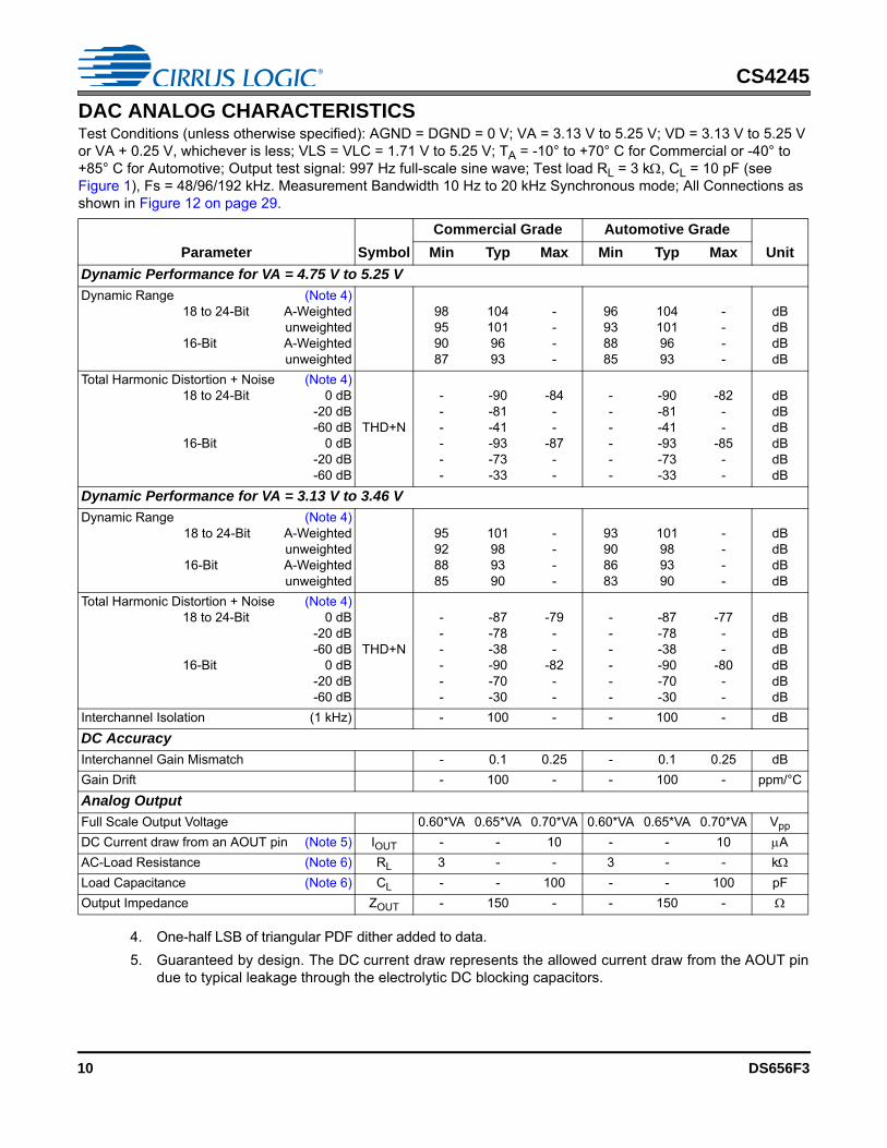
DAC ANALOG CHARACTERISTICSTest Conditions (unless otherwise specified): AGND = DGND = 0 V; VA = 3.13 V to 5.25 V; VD = 3.13 V to 5.25 V or VA + 0.25 V, whichever is less; VLS = VLC = 1.71 V to 5.25 V; TA = -10° to +70° C for Commercial or -40° to +85° C for Automotive; Output test signal: 997 Hz full-scale sine wave; Test load RL = 3 k, CL = 10 pF (see Figure 1), Fs = 48/96/192 kHz. Measurement Bandwidth 10 Hz to 20 kHz Synchronous mode; All Connections as shown in Figure 12 on page 29.
4. One-half LSB of triangular PDF dither added to data.5. Guaranteed by design. The DC current draw represents the allowed current draw from the AOUT pin
due to typical leakage through the electrolytic DC blocking capacitors.
Parameter
Commercial Grade Automotive Grade
Symbol Min Typ Max Min Typ Max Unit
Dynamic Performance for VA = 4.75 V to 5.25 V
Dynamic Range (Note 4)18 to 24-Bit A-Weighted
unweighted16-Bit A-Weighted
unweighted
98959087
1041019693
----
96938885
1041019693
----
dBdBdBdB
Total Harmonic Distortion + Noise (Note 4)18 to 24-Bit 0 dB
-20 dB-60 dB
16-Bit 0 dB-20 dB-60 dB
THD+N
------
-90-81-41-93-73-33
-84--
-87--
------
-90-81-41-93-73-33
-82--
-85--
dBdBdBdBdBdB
Dynamic Performance for VA = 3.13 V to 3.46 V
Dynamic Range (Note 4)18 to 24-Bit A-Weighted
unweighted16-Bit A-Weighted
unweighted
95928885
101989390
----
93908683
101989390
----
dBdBdBdB
Total Harmonic Distortion + Noise (Note 4)18 to 24-Bit 0 dB
-20 dB-60 dB
16-Bit 0 dB-20 dB-60 dB
THD+N
------
-87-78-38-90-70-30
-79--
-82--
------
-87-78-38-90-70-30
-77--
-80--
dBdBdBdBdBdB
Interchannel Isolation (1 kHz) - 100 - - 100 - dBDC Accuracy
Interchannel Gain Mismatch - 0.1 0.25 - 0.1 0.25 dBGain Drift - 100 - - 100 - ppm/°CAnalog Output
Full Scale Output Voltage 0.60*VA 0.65*VA 0.70*VA 0.60*VA 0.65*VA 0.70*VA VppDC Current draw from an AOUT pin (Note 5) IOUT - - 10 - - 10 AAC-Load Resistance (Note 6) RL 3 - - 3 - - kLoad Capacitance (Note 6) CL - - 100 - - 100 pFOutput Impedance ZOUT - 150 - - 150 -
10 DS656F3
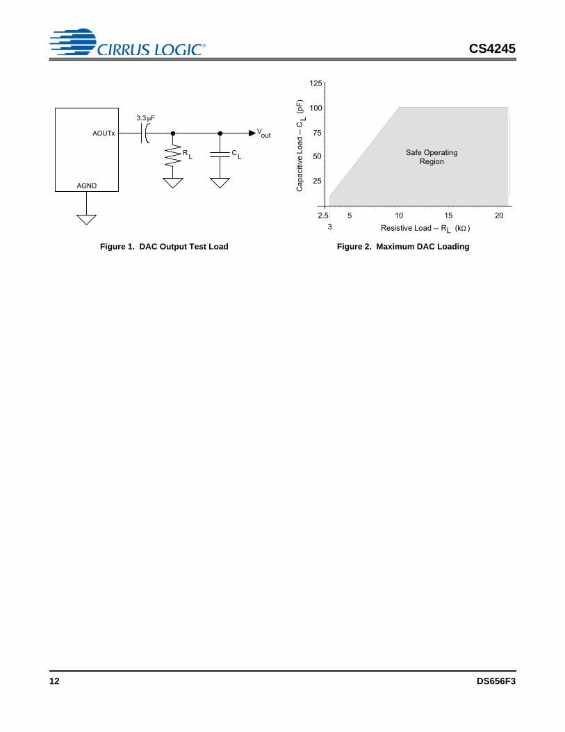
CS4245
6. Guaranteed by design. See Figure 2. RL and CL reflect the recommended minimum resistance andmaximum capacitance required for the internal op-amp’s stability. CL affects the dominant pole of theinternal output amp; increasing CL beyond 100 pF can cause the internal op-amp to become unstable.
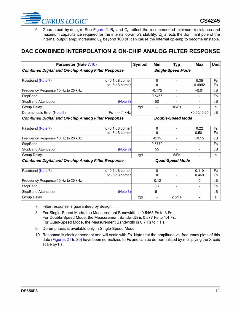
DAC COMBINED INTERPOLATION & ON-CHIP ANALOG FILTER RESPONSE
7. Filter response is guaranteed by design.8. For Single-Speed Mode, the Measurement Bandwidth is 0.5465 Fs to 3 Fs.
For Double-Speed Mode, the Measurement Bandwidth is 0.577 Fs to 1.4 Fs.For Quad-Speed Mode, the Measurement Bandwidth is 0.7 Fs to 1 Fs.
9. De-emphasis is available only in Single-Speed Mode.10. Response is clock dependent and will scale with Fs. Note that the amplitude vs. frequency plots of this
data (Figures 21 to 30) have been normalized to Fs and can be de-normalized by multiplying the X-axisscale by Fs.
Parameter (Note 7,10) Symbol Min Typ Max Unit
Combined Digital and On-chip Analog Filter Response Single-Speed Mode
Passband (Note 7) to -0.1 dB cornerto -3 dB corner
00
--
0.350.4992
FsFs
Frequency Response 10 Hz to 20 kHz -0.175 - +0.01 dBStopBand 0.5465 - - FsStopBand Attenuation (Note 8) 50 - - dBGroup Delay tgd - 10/Fs - sDe-emphasis Error (Note 9) Fs = 44.1 kHz - - +0.05/-0.25 dBCombined Digital and On-chip Analog Filter Response Double-Speed Mode
Passband (Note 7) to -0.1 dB cornerto -3 dB corner
00
--
0.220.501
FsFs
Frequency Response 10 Hz to 20 kHz -0.15 - +0.15 dBStopBand 0.5770 - - FsStopBand Attenuation (Note 8) 55 - - dBGroup Delay tgd - 5/Fs - sCombined Digital and On-chip Analog Filter Response Quad-Speed Mode
Passband (Note 7) to -0.1 dB cornerto -3 dB corner
00
--
0.1100.469
FsFs
Frequency Response 10 Hz to 20 kHz -0.12 - 0 dBStopBand 0.7 - - FsStopBand Attenuation (Note 8) 51 - - dBGroup Delay tgd - 2.5/Fs - s
DS656F3 11
CS4245
AOUTx
AGND
3.3µF
Vout
R L CL
Figure 1. DAC Output Test Load Figure 2. Maximum DAC Loading
100
50
75
25
2.5 5 10 15
Safe OperatingRegion
Cap
aciti
ve L
oad
-- C
(p
F)L
Resistive Load -- R (k )L
125
320
12 DS656F3
CS4245
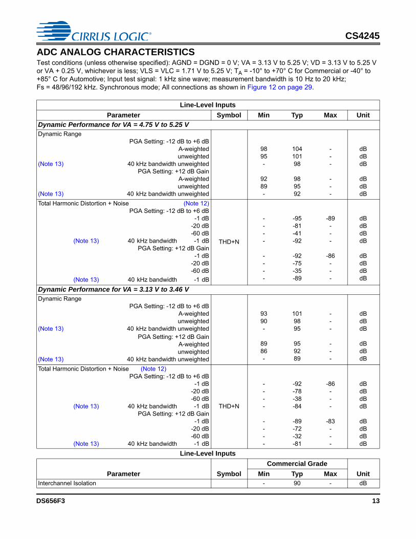
ADC ANALOG CHARACTERISTICS Test conditions (unless otherwise specified): AGND = DGND = 0 V; VA = 3.13 V to 5.25 V; VD = 3.13 V to 5.25 V or VA + 0.25 V, whichever is less; VLS = VLC = 1.71 V to 5.25 V; TA = -10° to +70° C for Commercial or -40° to +85° C for Automotive; Input test signal: 1 kHz sine wave; measurement bandwidth is 10 Hz to 20 kHz; Fs = 48/96/192 kHz. Synchronous mode; All connections as shown in Figure 12 on page 29.
Line-Level Inputs
Parameter Symbol Min Typ Max Unit
Dynamic Performance for VA = 4.75 V to 5.25 VDynamic Range
PGA Setting: -12 dB to +6 dBA-weightedunweighted
(Note 13) 40 kHz bandwidth unweightedPGA Setting: +12 dB Gain
A-weightedunweighted
(Note 13) 40 kHz bandwidth unweighted
9895-
9289-
10410198
989592
---
---
dBdBdB
dBdBdB
Total Harmonic Distortion + Noise (Note 12)PGA Setting: -12 dB to +6 dB
-1 dB-20 dB-60 dB
(Note 13) 40 kHz bandwidth -1 dBPGA Setting: +12 dB Gain
-1 dB-20 dB-60 dB
(Note 13) 40 kHz bandwidth -1 dB
THD+N
----
----
-95-81-41-92
-92-75-35-89
-89---
-86---
dBdBdBdB
dBdBdBdB
Dynamic Performance for VA = 3.13 V to 3.46 VDynamic Range
PGA Setting: -12 dB to +6 dBA-weightedunweighted
(Note 13) 40 kHz bandwidth unweightedPGA Setting: +12 dB Gain
A-weightedunweighted
(Note 13) 40 kHz bandwidth unweighted
9390-
8986-
1019895
959289
---
---
dBdBdB
dBdBdB
Total Harmonic Distortion + Noise (Note 12)PGA Setting: -12 dB to +6 dB
-1 dB-20 dB-60 dB
(Note 13) 40 kHz bandwidth -1 dBPGA Setting: +12 dB Gain
-1 dB-20 dB-60 dB
(Note 13) 40 kHz bandwidth -1 dB
THD+N
----
----
-92-78-38-84
-89-72-32-81
-86---
-83---
dBdBdBdB
dBdBdBdB
Line-Level Inputs
Parameter Symbol
Commercial Grade
UnitMin Typ MaxInterchannel Isolation - 90 - dB
DS656F3 13
CS4245
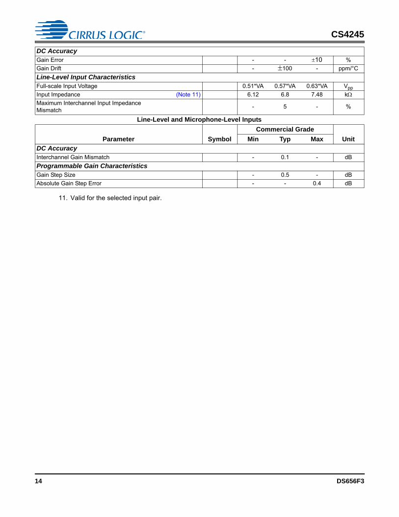
11. Valid for the selected input pair.
DC AccuracyGain Error - - 10 %Gain Drift - 100 - ppm/°CLine-Level Input CharacteristicsFull-scale Input Voltage 0.51*VA 0.57*VA 0.63*VA VppInput Impedance (Note 11) 6.12 6.8 7.48 kMaximum Interchannel Input ImpedanceMismatch - 5 - %
Line-Level and Microphone-Level Inputs
Parameter Symbol
Commercial Grade
UnitMin Typ Max
DC AccuracyInterchannel Gain Mismatch - 0.1 - dBProgrammable Gain CharacteristicsGain Step Size - 0.5 - dBAbsolute Gain Step Error - - 0.4 dB
14 DS656F3
CS4245
ADC ANALOG CHARACTERISTICS (Continued)
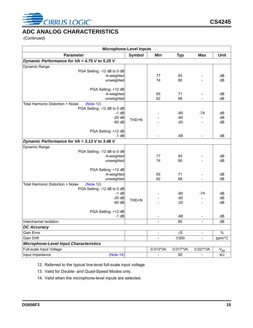
12. Referred to the typical line-level full-scale input voltage13. Valid for Double- and Quad-Speed Modes only.14. Valid when the microphone-level inputs are selected.
Microphone-Level Inputs
Parameter Symbol Min Typ Max Unit
Dynamic Performance for VA = 4.75 V to 5.25 VDynamic Range
PGA Setting: -12 dB to 0 dBA-weightedunweighted
PGA Setting: +12 dBA-weightedunweighted
7774
6562
8380
7168
--
--
dBdB
dBdB
Total Harmonic Distortion + Noise (Note 12)PGA Setting: -12 dB to 0 dB
-1 dB-20 dB-60 dB
PGA Setting: +12 dB -1 dB
THD+N
---
-
-80-60-20
-68
-74--
-
dBdBdB
dBDynamic Performance for VA = 3.13 V to 3.46 VDynamic Range
PGA Setting: -12 dB to 0 dBA-weightedunweighted
PGA Setting: +12 dBA-weightedunweighted
7774
6562
8380
7168
--
--
dBdB
dBdB
Total Harmonic Distortion + Noise (Note 12)PGA Setting: -12 dB to 0 dB
-1 dB-20 dB-60 dB
PGA Setting: +12 dB -1 dB
THD+N
---
-
-80-60-20
-68
-74--
-
dBdBdB
dBInterchannel Isolation - 80 - dBDC AccuracyGain Error - 5 - %Gain Drift - 300 - ppm/°CMicrophone-Level Input CharacteristicsFull-scale Input Voltage 0.013*VA 0.017*VA 0.021*VA VppInput Impedance (Note 14) - 60 - k
DS656F3 15
CS4245
ADC DIGITAL FILTER CHARACTERISTICS
15. Filter response is guaranteed by design.16. Response shown is for Fs = 48 kHz. 17. Response is clock-dependent and will scale with Fs. Note that the response plots (Figures 33 to 44) are
normalized to Fs and can be de-normalized by multiplying the X-axis scale by Fs.
Parameter (Notes 15, 17) Symbol Min Typ Max Unit
Single-Speed Mode
Passband (-0.1 dB) 0 - 0.4896 FsPassband Ripple - - 0.035 dBStopband 0.5688 - - FsStopband Attenuation 70 - - dBTotal Group Delay (Fs = Output Sample Rate) tgd - 12/Fs - sDouble-Speed Mode
Passband (-0.1 dB) 0 - 0.4896 FsPassband Ripple - - 0.025 dBStopband 0.5604 - - FsStopband Attenuation 69 - - dBTotal Group Delay (Fs = Output Sample Rate) tgd - 9/Fs - sQuad-Speed Mode
Passband (-0.1 dB) 0 - 0.2604 FsPassband Ripple - - 0.025 dBStopband 0.5000 - - FsStopband Attenuation 60 - - dBTotal Group Delay (Fs = Output Sample Rate) tgd - 5/Fs - sHigh-Pass Filter Characteristics
Frequency Response -3.0 dB-0.13 dB (Note 16)
- 120
--
HzHz
Phase Deviation @ 20 Hz (Note 16) - 10 - DegPassband Ripple - - 0 dB
Filter Settling Time 105/Fs s
16 DS656F3
CS4245
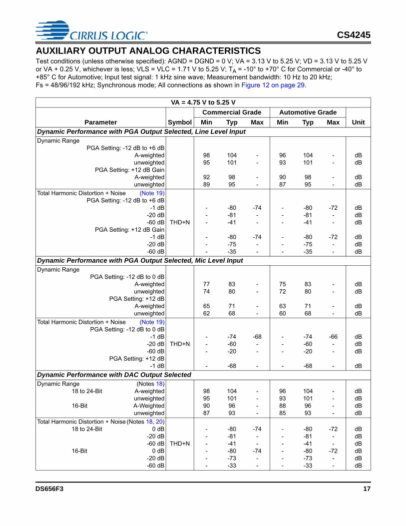
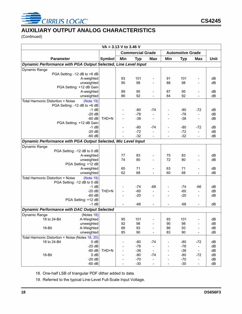
AUXILIARY OUTPUT ANALOG CHARACTERISTICS Test conditions (unless otherwise specified): AGND = DGND = 0 V; VA = 3.13 V to 5.25 V; VD = 3.13 V to 5.25 V or VA + 0.25 V, whichever is less; VLS = VLC = 1.71 V to 5.25 V; TA = -10° to +70° C for Commercial or -40° to +85° C for Automotive; Input test signal: 1 kHz sine wave; Measurement bandwidth: 10 Hz to 20 kHz; Fs = 48/96/192 kHz; Synchronous mode; All connections as shown in Figure 12 on page 29.
VA = 4.75 V to 5.25 V
Parameter Symbol
Commercial Grade Automotive Grade
UnitMin Typ Max Min Typ Max
Dynamic Performance with PGA Output Selected, Line Level InputDynamic Range
PGA Setting: -12 dB to +6 dBA-weightedunweighted
PGA Setting: +12 dB GainA-weightedunweighted
9895
9289
104101
9895
--
--
9693
9087
104101
9895
--
--
dBdB
dBdB
Total Harmonic Distortion + Noise (Note 19)PGA Setting: -12 dB to +6 dB
-1 dB-20 dB-60 dB
PGA Setting: +12 dB Gain -1 dB
-20 dB-60 dB
THD+N
---
---
-80-81-41
-80-75-35
-74--
-74--
---
---
-80-81-41
-80-75-35
-72--
-72--
dBdBdB
dBdBdB
Dynamic Performance with PGA Output Selected, Mic Level InputDynamic Range
PGA Setting: -12 dB to 0 dBA-weightedunweighted
PGA Setting: +12 dBA-weightedunweighted
7774
6562
8380
7168
--
--
7572
6360
8380
7168
--
--
dBdB
dBdB
Total Harmonic Distortion + Noise (Note 19)PGA Setting: -12 dB to 0 dB
-1 dB-20 dB-60 dB
PGA Setting: +12 dB -1 dB
THD+N---
-
-74-60-20
-68
-68--
-
---
-
-74-60-20
-68
-66--
-
dBdBdB
dBDynamic Performance with DAC Output SelectedDynamic Range (Notes 18)
18 to 24-Bit A-weightedunweighted
16-Bit A-Weightedunweighted
98959087
1041019693
----
96938885
1041019693
----
dBdBdBdB
Total Harmonic Distortion + Noise (Notes 18, 20)18 to 24-Bit 0 dB
-20 dB-60 dB
16-Bit 0 dB-20 dB-60 dB
THD+N
------
-80-81-41-80-73-33
-74--
-74--
------
-80-81-41-80-73-33
-72--
-72--
dBdBdBdBdBdB
DS656F3 17
CS4245
AUXILIARY OUTPUT ANALOG CHARACTERISTICS (Continued)
18. One-half LSB of triangular PDF dither added to data.19. Referred to the typical Line-Level Full-Scale Input Voltage.
VA = 3.13 V to 3.46 V
Parameter Symbol
Commercial Grade Automotive Grade
UnitMin Typ Max Min Typ Max
Dynamic Performance with PGA Output Selected, Line Level InputDynamic Range
PGA Setting: -12 dB to +6 dBA-weightedunweighted
PGA Setting: +12 dB GainA-weightedunweighted
9390
8986
10198
9592
--
--
9188
8784
10198
9592
--
--
dBdB
dBdB
Total Harmonic Distortion + Noise (Note 19)PGA Setting: -12 dB to +6 dB
-1 dB-20 dB-60 dB
PGA Setting: +12 dB Gain -1 dB-20 dB-60 dB
THD+N
---
---
-80-78-38
-80-72-32
-74--
-74--
---
---
-80-78-38
-80-72-32
-72--
-72--
dBdBdB
dBdBdB
Dynamic Performance with PGA Output Selected, Mic Level InputDynamic Range
PGA Setting: -12 dB to 0 dBA-weightedunweighted
PGA Setting: +12 dBA-weightedunweighted
7774
6562
8380
7168
--
--
7572
6360
8380
7168
--
--
dBdB
dBdB
Total Harmonic Distortion + Noise (Note 19)PGA Setting: -12 dB to 0 dB
-1 dB-20 dB-60 dB
PGA Setting: +12 dB -1 dB
THD+N---
-
-74-60-20
-68
-68--
-
---
-
-74-60-20
-68
-66--
-
dBdBdB
dBDynamic Performance with DAC Output SelectedDynamic Range (Notes 18)
18 to 24-Bit A-Weightedunweighted
16-Bit A-Weightedunweighted
95928885
101989390
----
93908683
101989390
----
dBdBdBdB
Total Harmonic Distortion + Noise (Notes 18, 20)18 to 24-Bit 0 dB
-20 dB-60 dB
16-Bit 0 dB-20 dB-60 dB
THD+N
------
-80-78-38-80-70-30
-74--
-74--
------
-80-78-38-80-70-30
-72--
-72--
dBdBdBdBdBdB
18 DS656F3
CS4245
20. Referred to the typical DAC Full-Scale Output Voltage.
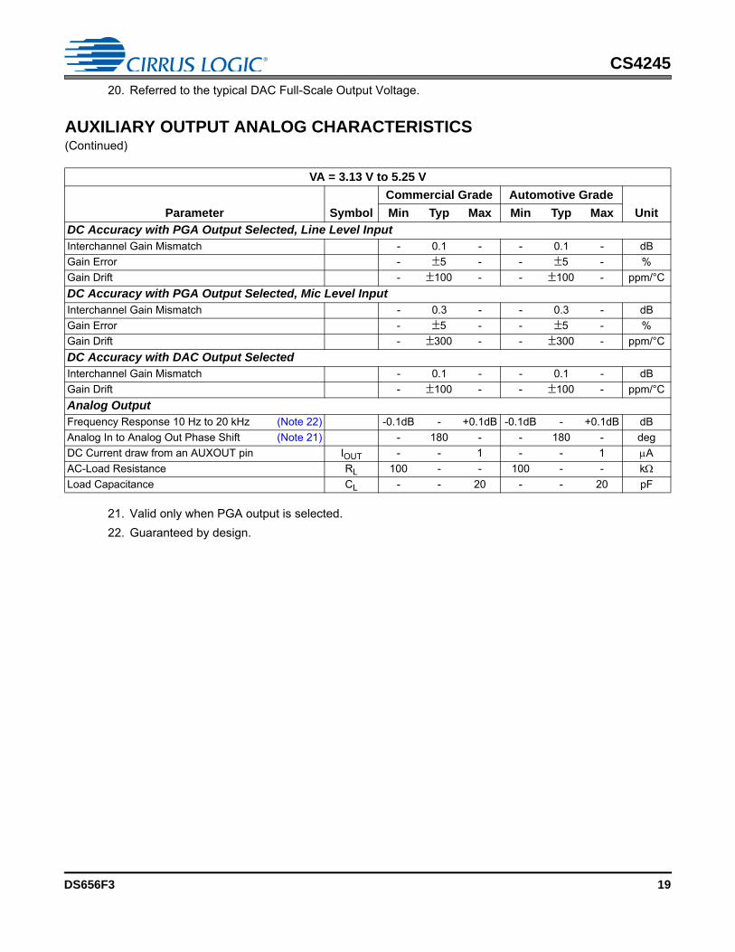
AUXILIARY OUTPUT ANALOG CHARACTERISTICS (Continued)
21. Valid only when PGA output is selected.22. Guaranteed by design.
VA = 3.13 V to 5.25 V
Parameter Symbol
Commercial Grade Automotive Grade
UnitMin Typ Max Min Typ Max
DC Accuracy with PGA Output Selected, Line Level InputInterchannel Gain Mismatch - 0.1 - - 0.1 - dBGain Error - 5 - - 5 - %Gain Drift - 100 - - 100 - ppm/°CDC Accuracy with PGA Output Selected, Mic Level InputInterchannel Gain Mismatch - 0.3 - - 0.3 - dBGain Error - 5 - - 5 - %Gain Drift - 300 - - 300 - ppm/°CDC Accuracy with DAC Output SelectedInterchannel Gain Mismatch - 0.1 - - 0.1 - dBGain Drift - 100 - - 100 - ppm/°CAnalog OutputFrequency Response 10 Hz to 20 kHz (Note 22) -0.1dB - +0.1dB -0.1dB - +0.1dB dBAnalog In to Analog Out Phase Shift (Note 21) - 180 - - 180 - degDC Current draw from an AUXOUT pin IOUT - - 1 - - 1 AAC-Load Resistance RL 100 - - 100 - - kLoad Capacitance CL - - 20 - - 20 pF
DS656F3 19
CS4245
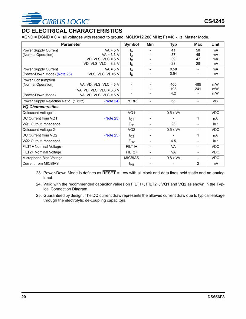
DC ELECTRICAL CHARACTERISTICSAGND = DGND = 0 V, all voltages with respect to ground. MCLK=12.288 MHz; Fs=48 kHz; Master Mode.
23. Power-Down Mode is defines as RESET = Low with all clock and data lines held static and no analoginput.
24. Valid with the recommended capacitor values on FILT1+, FILT2+, VQ1 and VQ2 as shown in the Typ-ical Connection Diagram.
25. Guaranteed by design. The DC current draw represents the allowed current draw due to typical leakagethrough the electrolytic de-coupling capacitors.
Parameter Symbol Min Typ Max Unit
Power Supply Current VA = 5 V(Normal Operation) VA = 3.3 V
VD, VLS, VLC = 5 VVD, VLS, VLC = 3.3 V
IAIAIDID
----
41373923
50454728
mAmAmAmA
Power Supply Current VA = 5 V(Power-Down Mode) (Note 23) VLS, VLC, VD=5 V
IAID
--
0.500.54
--
mAmA
Power Consumption(Normal Operation) VA, VD, VLS, VLC = 5 V
VA, VD, VLS, VLC = 3.3 V(Power-Down Mode) VA, VD, VLS, VLC = 5 V
---
---
4001984.2
485241
-
mWmWmW
Power Supply Rejection Ratio (1 kHz) (Note 24) PSRR - 55 - dBVQ Characteristics
Quiescent Voltage 1 VQ1 - 0.5 x VA - VDCDC Current from VQ1 (Note 25) IQ1 - - 1 AVQ1 Output Impedance ZQ1 - 23 - kQuiescent Voltage 2 VQ2 - 0.5 x VA - VDCDC Current from VQ2 (Note 25) IQ2 - - 1 AVQ2 Output Impedance ZQ2 - 4.5 - kFILT1+ Nominal Voltage FILT1+ - VA - VDCFILT2+ Nominal Voltage FILT2+ - VA - VDCMicrophone Bias Voltage MICBIAS - 0.8 x VA - VDCCurrent from MICBIAS IMB - - 2 mA
20 DS656F3
CS4245
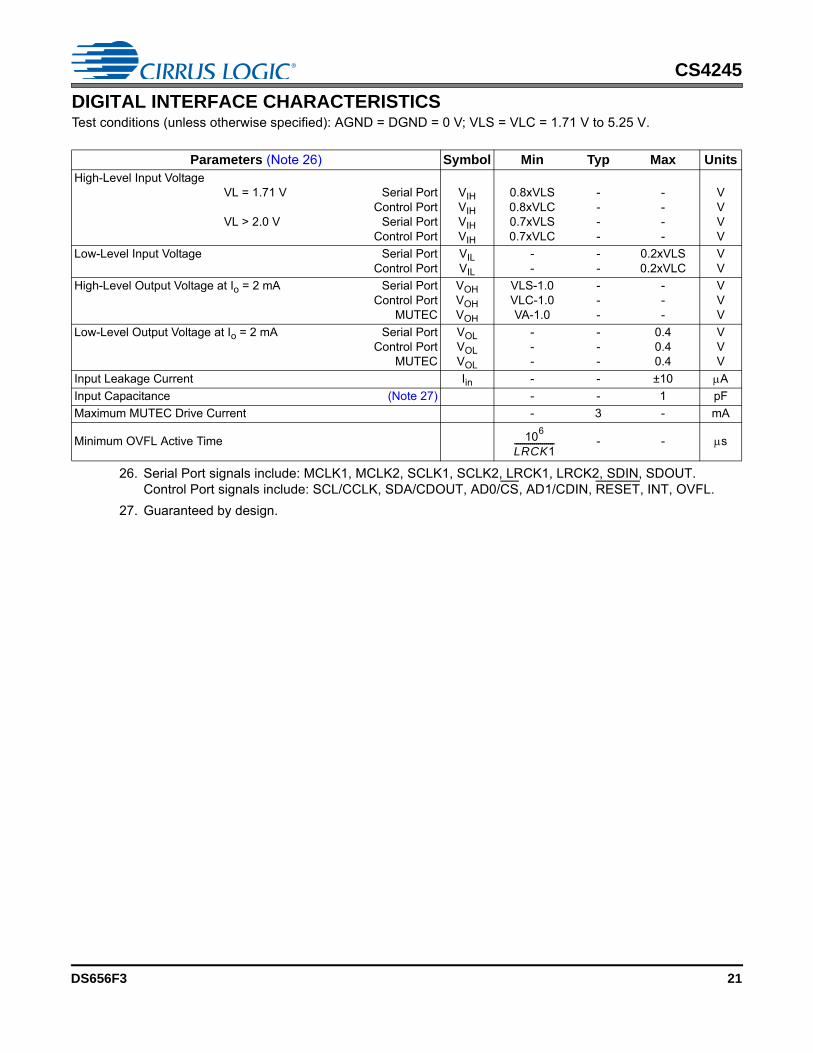
DIGITAL INTERFACE CHARACTERISTICSTest conditions (unless otherwise specified): AGND = DGND = 0 V; VLS = VLC = 1.71 V to 5.25 V.
26. Serial Port signals include: MCLK1, MCLK2, SCLK1, SCLK2, LRCK1, LRCK2, SDIN, SDOUT.Control Port signals include: SCL/CCLK, SDA/CDOUT, AD0/CS, AD1/CDIN, RESET, INT, OVFL.
27. Guaranteed by design.
Parameters (Note 26) Symbol Min Typ Max UnitsHigh-Level Input Voltage
VL = 1.71 V Serial PortControl Port
VL > 2.0 V Serial PortControl Port
VIHVIHVIHVIH
0.8xVLS0.8xVLC0.7xVLS0.7xVLC
----
----
VVVV
Low-Level Input Voltage Serial PortControl Port
VILVIL
--
--
0.2xVLS0.2xVLC
VV
High-Level Output Voltage at Io = 2 mA Serial PortControl Port
MUTEC
VOHVOHVOH
VLS-1.0VLC-1.0VA-1.0
---
---
VVV
Low-Level Output Voltage at Io = 2 mA Serial Port Control Port MUTEC
VOLVOLVOL
---
---
0.40.40.4
VVV
Input Leakage Current Iin - - ±10 AInput Capacitance (Note 27) - - 1 pFMaximum MUTEC Drive Current - 3 - mA
Minimum OVFL Active Time - - s106
LRCK1--------------------
DS656F3 21
CS4245
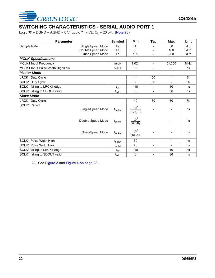
SWITCHING CHARACTERISTICS - SERIAL AUDIO PORT 1Logic ‘0’ = DGND = AGND = 0 V; Logic ‘1’ = VL, CL = 20 pF. (Note 28)
28. See Figure 3 and Figure 4 on page 23.
Parameter Symbol Min Typ Max UnitSample Rate Single Speed Mode
Double Speed ModeQuad Speed Mode
FsFsFs
450
100
---
50100200
kHzkHzkHz
MCLK SpecificationsMCLK1 Input Frequency fmclk 1.024 - 51.200 MHzMCLK1 Input Pulse Width High/Low tclkhl 8 - - nsMaster ModeLRCK1 Duty Cycle - 50 - %SCLK1 Duty Cycle - 50 - %SCLK1 falling to LRCK1 edge tslr -10 - 10 nsSCLK1 falling to SDOUT valid tsdo 0 - 36 nsSlave ModeLRCK1 Duty Cycle 40 50 60 %SCLK1 Period
Single-Speed Mode
Double-Speed Mode
Quad-Speed Mode
tsclkw
tsclkw
tsclkw
-
-
-
-
-
-
ns
ns
ns
SCLK1 Pulse Width High tsclkh 30 - - nsSCLK1 Pulse Width Low tsclkl 48 - - nsSCLK1 falling to LRCK1 edge tslr -10 - 10 nsSCLK1 falling to SDOUT valid tsdo 0 - 36 ns
109
128 Fs---------------------
109
64 Fs------------------
109
64 Fs------------------
22 DS656F3
CS4245
slrt
SDOUT
SCLK1Output
LRCK1Output
sdot
slrt
SDOUT
SCLK1Input
LRCK1Input
sdot
sclkht sclklt
sclkwt
Figure 3. Master Mode Timing - Serial Audio Port 1
Figure 4. Slave Mode Timing - Serial Audio Port 1
DS656F3 23
CS4245
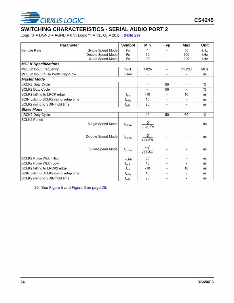
SWITCHING CHARACTERISTICS - SERIAL AUDIO PORT 2Logic ‘0’ = DGND = AGND = 0 V; Logic ‘1’ = VL, CL = 20 pF. (Note 29)
29. See Figure 5 and Figure 6 on page 25.
Parameter Symbol Min Typ Max UnitSample Rate Single Speed Mode
Double Speed ModeQuad Speed Mode
FsFsFs
450
100
---
50100200
kHzkHzkHz
MCLK SpecificationsMCLK2 Input Frequency fmclk 1.024 - 51.200 MHzMCLK2 Input Pulse Width High/Low tclkhl 8 - - nsMaster ModeLRCK2 Duty Cycle - 50 - %SCLK2 Duty Cycle - 50 - %SCLK2 falling to LRCK edge tslr -10 - 10 nsSDIN valid to SCLK2 rising setup time tsdis 16 - - nsSCLK2 rising to SDIN hold time tsdih 20 - - nsSlave ModeLRCK2 Duty Cycle 40 50 60 %SCLK2 Period
Single-Speed Mode
Double-Speed Mode
Quad-Speed Mode
tsclkw
tsclkw
tsclkw
-
-
-
-
-
-
ns
ns
ns
SCLK2 Pulse Width High tsclkh 30 - - nsSCLK2 Pulse Width Low tsclkl 48 - - nsSCLK2 falling to LRCK2 edge tslr -10 - 10 nsSDIN valid to SCLK2 rising setup time tsdis 16 - - nsSCLK2 rising to SDIN hold time tsdih 20 - - ns
109
128 Fs---------------------
109
64 Fs------------------
109
64 Fs------------------
24 DS656F3
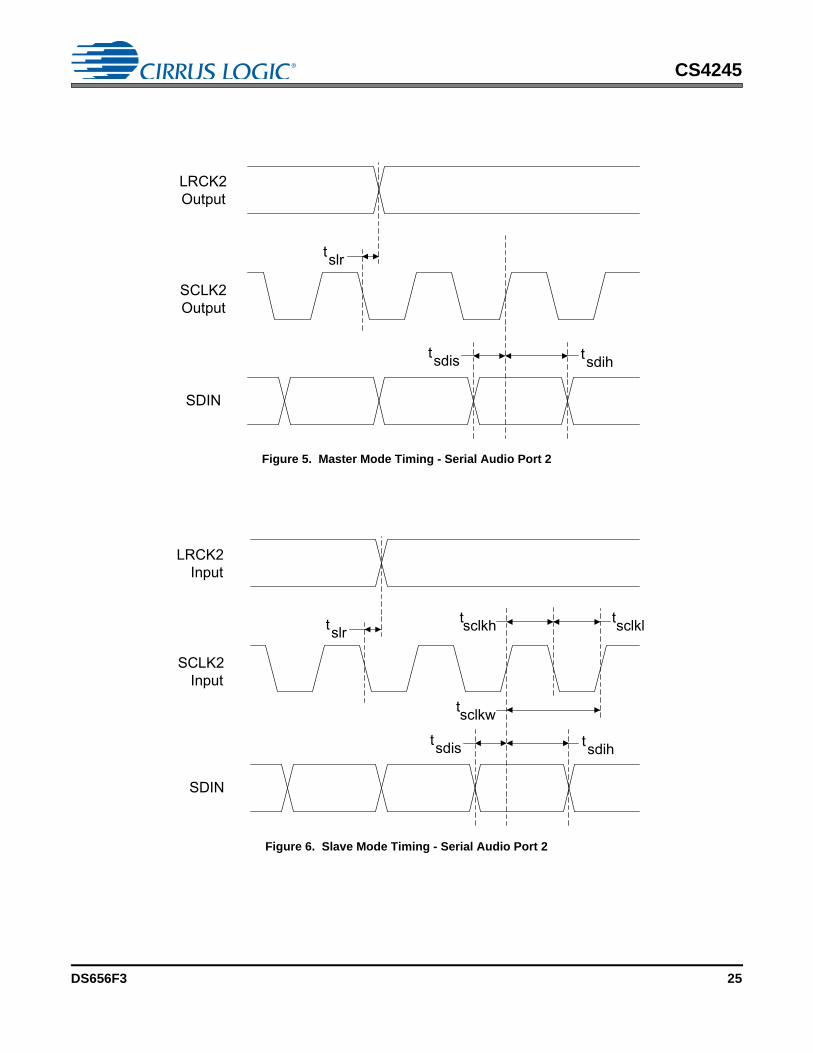
CS4245
sdist
slrt
SCLK2Output
LRCK2Output
SDIN
sdiht
sdist
slrt
SCLK2Input
LRCK2Input
SDIN
sdiht
sclkht sclklt
sclkwt
Figure 5. Master Mode Timing - Serial Audio Port 2
Figure 6. Slave Mode Timing - Serial Audio Port 2
DS656F3 25
CS4245
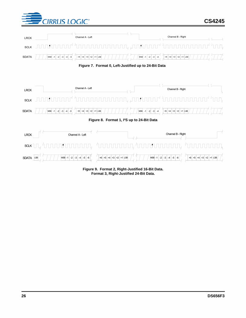
Figure 7. Format 0, Left-Justified up to 24-Bit Data
LRCK
SCLK
SDATA +3 +2 +1+5 +4-1 -2 -3 -4 -5 +3 +2 +1+5 +4MSB -1 -2 -3 -4
Channel A - Left Channel B - Right
LSBLSBMSB
Figure 8. Format 1, I²S up to 24-Bit Data
LRCK
SCLK
SDATA +3 +2 +1+5 +4MSB -1 -2 -3 -4 -5 +3 +2 +1+5 +4-1 -2 -3 -4
Channel A - Left Channel B - Right
LSB MSB LSB
LRCK
SCLK
SDATA +5 +4 +3 +2 +1-1 -2 -3 -4 -5 +5 +4 +3 +2 +1-1 -2 -3 -4 -5+6-6 +6-6
Channel A - Left Channel B - Right
MSB LSB MSB LSBLSB
Figure 9. Format 2, Right-Justified 16-Bit Data.Format 3, Right-Justified 24-Bit Data.
26 DS656F3
CS4245
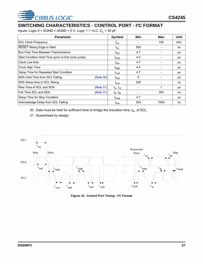
SWITCHING CHARACTERISTICS - CONTROL PORT - I²C FORMATInputs: Logic 0 = DGND = AGND = 0 V, Logic 1 = VLC, CL = 30 pF.
30. Data must be held for sufficient time to bridge the transition time, tfc, of SCL.31. Guaranteed by design.
Parameter Symbol Min Max Unit
SCL Clock Frequency fscl - 100 kHz
RESET Rising Edge to Start tirs 500 - ns
Bus Free Time Between Transmissions tbuf 4.7 - µs
Start Condition Hold Time (prior to first clock pulse) thdst 4.0 - µs
Clock Low time tlow 4.7 - µs
Clock High Time thigh 4.0 - µs
Setup Time for Repeated Start Condition tsust 4.7 - µs
SDA Hold Time from SCL Falling (Note 30) thdd 0 - µs
SDA Setup time to SCL Rising tsud 250 - ns
Rise Time of SCL and SDA (Note 31) trc, trd - 1 µs
Fall Time SCL and SDA (Note 31) tfc, tfd - 300 ns
Setup Time for Stop Condition tsusp 4.7 - µs
Acknowledge Delay from SCL Falling tack 300 1000 ns
t buf t hdst
tlow
thdd
t high
t sud
Stop Start
SDA
S CL
t irs
RS T
t hdst
t rc
t fc
t sust
t susp
Start StopRepeated
t rd t fd
t ack
Figure 10. Control Port Timing - I²C Format
DS656F3 27
CS4245
SWITCHING CHARACTERISTICS - CONTROL PORT - SPI FORMAT Inputs: Logic 0 = DGND = AGND = 0 V, Logic 1 = VLC, CL = 30 pF.
32. Data must be held for sufficient time to bridge the transition time of CCLK.33. For fsck <1 MHz.
Parameter Symbol Min Max Units
CCLK Clock Frequency fsck - 6.0 MHz
RESET Rising Edge to CS Falling tsrs 500 - ns
CS High Time Between Transmissions tcsh 1.0 - s
CS Falling to CCLK Edge tcss 20 - ns
CCLK Low Time tscl 66 - ns
CCLK High Time tsch 66 - ns
CDIN to CCLK Rising Setup Time tdsu 40 - ns
CCLK Rising to DATA Hold Time (Note 32) tdh 15 - ns
CCLK Falling to CDOUT Stable tpd - 50 ns
Rise Time of CDOUT tr1 - 25 ns
Fall Time of CDOUT tf1 - 25 ns
Rise Time of CCLK and CDIN (Note 33) tr2 - 100 ns
Fall Time of CCLK and CDIN (Note 33) tf2 - 100 ns
t r2 t f2
t dsu t dh
t scht scl
CS
CCLK
CDIN
t css
t pd
CDOUT
tcsh
RST t srs
Figure 11. Control Port Timing - SPI Format
28 DS656F3
CS4245
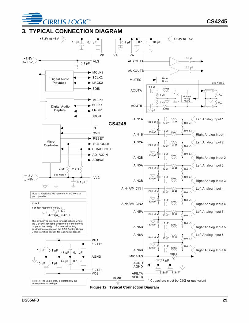
3. TYPICAL CONNECTION DIAGRAM
VLS0.1 µF+1.8Vto +5V
MUTEC MuteDrive
DGND
VLC0.1 µF
+1.8Vto +5V
SCL/CCLK
SDA/CDOUT
AD1/CDIN
RESET
2 k
See Note 1
LRCK2
SDIN
AGND
AD0/CS
Note 1: Resistors are required for I²C control port operation
Digital Audio Playback
Micro-Controller
MCLK2SCLK2
* Capacitors must be C0G or equivalent
Digital Audio Capture LRCK1
SDOUT
MCLK1
SCLK1
AUXOUTA
AUXOUTB
2.2nFAFILTAAFILTB
OVFL
2.2nF
3.3 µF
3.3 µF
47 µF0.1 µF
VQ1FILT1+
10 µF
AGND
* *
AOUTA
AOUTB
470
4703.3 µF
COptionalAnalog Muting
2 k
3.3 µF
INT
47 µF
10 k
10 k C Rext
Rext
See Note 2
For best response to Fs/2 :
4704
470
ext
ext
RFs
RC
This circuitry is intended for applications where the CS4245 connects directly to an unbalanced output of the design . For internal routing applications please see the DAC Analog Output Characteristics section for loading limitations .
Note 2 :
AIN1A Left Analog Input 110 µF
10 µF
1800 pF
1800 pF
100 k
100 k100
100
AIN1B Right Analog Input 1
AIN2A Left Analog Input 210 µF
10 µF
1800 pF
1800 pF
100 k
100 k100
100
AIN2B Right Analog Input 2
AIN3A Left Analog Input 310 µF
10 µF
1800 pF
1800 pF
100 k
100 k100
100
AIN3B Right Analog Input 3
AIN4A/MICIN1 Left Analog Input 410 µF
10 µF
1800 pF
1800 pF
100 k
100 k100
100
AIN4B/MICIN2 Right Analog Input 4
AIN5A Left Analog Input 510 µF
10 µF
1800 pF
1800 pF
100 k
100 k100
100
AIN5B Right Analog Input 5
AIN6A Left Analog Input 610 µF
10 µF
1800 pF
1800 pF
100 k
100 k100
100
AIN6B Right Analog Input 6
MICBIAS
AGND
0.1 µF
47 µF0.1 µF
VQ2FILT2+
10 µF0.1 µF
*
*
*
*
*
*
*
*
*
*
*
*
*
*
0.1 µF
VA
10 µF+3.3V to +5V
0.1 µF10 µF 0.1 µF
VAVD
+3.3V to +5V
RL
Note 3
Note 3: The value of RL is dictated by the microphone carteridge.
CS4245
Figure 12. Typical Connection Diagram
DS656F3 29
CS4245
4. APPLICATIONS
4.1 Recommended Power-Up Sequence1. Hold RESET low until the power supply, MCLK1, MCLK2 (if used), LRCK1 and LRCK2 are stable. In
this state, the Control Port is reset to its default settings. 2. Bring RESET high. The device will remain in a low power state with the PDN bit set by default. The con-
trol port will be accessible.3. The desired register settings can be loaded while the PDN bit remains set.4. Clear the PDN bit to initiate the power-up sequence.
4.2 System Clocking
The CS4245 will operate at sampling frequencies from 4 kHz to 200 kHz. This range is divided into threespeed modes as shown in Table 1.
The CS4245 has two serial ports which may be operated synchronously or asynchronously. Serial port 1consists of the SCLK1 and LRCK1 signals and clocks the serial audio output, SDOUT. Serial port 2 consistsof the SCLK2 and LRCK2 signals and clocks the serial audio input, SDIN.
Each serial port may be independently placed into Single, Double, or Quad Speed mode. The serial portsmay also be independently placed into Master or Slave mode.
4.2.1 Synchronous / Asynchronous Mode
By default, the CS4245 operates in Synchronous Mode with both serial ports synchronous to MCLK1. In this mode, the serial ports may operate at different synchronous rates as set by the ADC_FM and DAC_FM bits, and MCLK2 does not need to be provided (the MCLK2 pin may be left unconnected).
If the Asynch bit is set (see “Asynchronous Mode (Bit 0)” on page 46), the CS4245 will operate in asyn-chronous mode. The serial ports will operate asynchronously with Serial Port 1 clocked from MCLK1 and Serial Port 2 clocked from MCLK2. In this mode, the serial ports may operate at different asynchronous rates.
4.2.2 Master Clock
In Asynchronous Mode, MCLK1/LRCK1 and MCLK2/LRCK2 must maintain an integer ratio. In synchro-nous mode MCLK1/LRCK1 and MCLK1/LRCK2 must maintain an integer ratio. Some common ratios are shown in Table 2.The LRCK frequency is equal to Fs, the frequency at which audio samples for each channel are clocked into or out of the device. The ADC_FM and DAC_FM bits and the MCLK Freq bits (See “MCLK Frequency - Address 05h” on page 45.) configure the device to generate the proper clocks
Mode Sampling Frequency
Single-Speed 4-50 kHzDouble-Speed 50-100 kHzQuad-Speed 100-200 kHz
Table 1. Speed Modes
30 DS656F3
CS4245
in Master Mode, and receive the proper clocks in Slave Mode. Table 2 illustrates several standard audio sample rates and the required MCLK and LRCK frequencies.
In both Master and Slave Modes, the external MCLK must be divided down based on the MCLK/LRCK ratio to achieve a post-divider MCLK/LRCK ratio of 256x for SSM, 128x for DSM, or 64x for QSM. Table 3 lists the appropriate dividers.
LRCK(kHz)
MCLK (MHz)
64x 96x 128x 192x 256x 384x 512x 768x 1024x
32 - - - - 8.1920 12.2880 16.3840 24.5760 32.768044.1 - - - - 11.2896 16.9344 22.5792 33.8680 45.158448 - - - - 12.2880 18.4320 24.5760 36.8640 49.152064 - - 8.1920 12.2880 16.3840 24.5760 32.7680 - -
88.2 - - 11.2896 16.9344 22.5792 33.8680 45.1584 - -96 - - 12.2880 18.4320 24.5760 36.8640 49.1520 - -128 8.1920 12.2880 16.3840 24.5760 32.7680 - - - -
176.4 11.2896 16.9344 22.5792 33.8680 45.1584 - - - -192 12.2880 18.4320 24.5760 36.8640 49.1520 - - - -
Mode QSM DSM SSM
Table 2. Common Clock Frequencies
MCLK/LRCK Ratio MCLK Dividers
64x - - ÷196x - - ÷1.5128x - ÷1 ÷2192x - ÷1.5 ÷3256x ÷1 ÷2 ÷4384x ÷1.5 ÷3 -512x ÷2 ÷4 -768x ÷3 - -1024x ÷4 - -Mode SSM DSM QSM
Table 3. MCLK Dividers
DS656F3 31
CS4245
4.2.3 Master Mode
As a clock master, LRCK and SCLK will operate as outputs. The two serial ports may be independently placed into Master or Slave mode. Each LRCK and SCLK is internally derived from its respective MCLK with LRCK equal to Fs and SCLK equal to 64 x Fs as shown in Figure 13.
4.2.4 Slave Mode
In Slave Mode, SCLK and LRCK operate as inputs. Each serial port may be independently placed into Slave Mode. The Left/Right clock signal must be equal to the sample rate, Fs. If operating in Asynchro-nous Mode, LRCK1 must be synchronously derived from MCLK1 and LRCK2 must be synchronously de-rived from MCLK2. If operating in Synchronous Mode, LRCK1, and LRCK2 must be synchronously derived from MCLK1. For more information on Synchronous and Asynchronous Modes, see “Synchro-nous / Asynchronous Mode” on page 30.
For each serial port, the serial bit clock must be equal to 128x, 64x, 48x or 32x Fs, depending on the de-sired speed mode. If operating in Asynchronous Mode, the serial bit clock SCLK1 must be synchronously derived from MCLK1 and SCLK2 must be synchronously derived from MCLK2. If operating in Synchro-nous Mode, SCLK1, and SCLK2 must be synchronously derived from MCLK1. Refer to Table 4 for re-quired serial bit clock to Left/Right clock ratios.
4.3 High-Pass Filter and DC Offset Calibration
When using operational amplifiers in the input circuitry driving the CS4245, a small DC offset may be driveninto the A/D converter. The CS4245 includes a high-pass filter after the decimator to remove any DC offsetwhich could result in recording a DC level, possibly yielding clicks when switching between devices in a mul-tichannel system.
Single-Speed Double-Speed Quad-Speed
SCLK/LRCK Ratio 32x, 48x, 64x, 128x 32x, 48x, 64x 32x, 48x, 64x
Table 4. Slave Mode Serial Bit Clock Ratios
÷256
÷128
÷64
÷4
÷2
÷1
00
01
10
00
01
10
LRCK1
SCLK1
000
001
010
÷1
÷1.5
÷2
011
100
÷3
÷4
MCLK1
÷256
÷128
÷64
÷4
÷2
÷1
00
01
10
00
01
10
000
001
010
÷1
÷1.5
÷2
011
100
÷3
÷4
MCLK2
LRCK2
SCLK2
0
1DAC_FM Bits
ADC_FM Bits
ASynch Bit
MCLK1 Freq Bits
MCLK2 Freq Bits
Figure 13. Master Mode Clocking
32 DS656F3
CS4245
The high-pass filter continuously subtracts a measure of the DC offset from the output of the decimationfilter. If the HPFFreeze bit (See “ADC High-Pass Filter Freeze (Bit 1)” on page 45.) is set during normal op-eration, the current value of the DC offset for the each channel is frozen and this DC offset will continue tobe subtracted from the conversion result. This feature makes it possible to perform a system DC offset cal-ibration by:1. Running the CS4245 with the high-pass filter enabled until the filter settles. See the ADC Digital Filter
Characteristics section for filter settling time. 2. Disabling the high-pass filter and freezing the stored DC offset.
A system calibration performed in this way will eliminate offsets anywhere in the signal path between thecalibration point and the CS4245.
DS656F3 33
CS4245
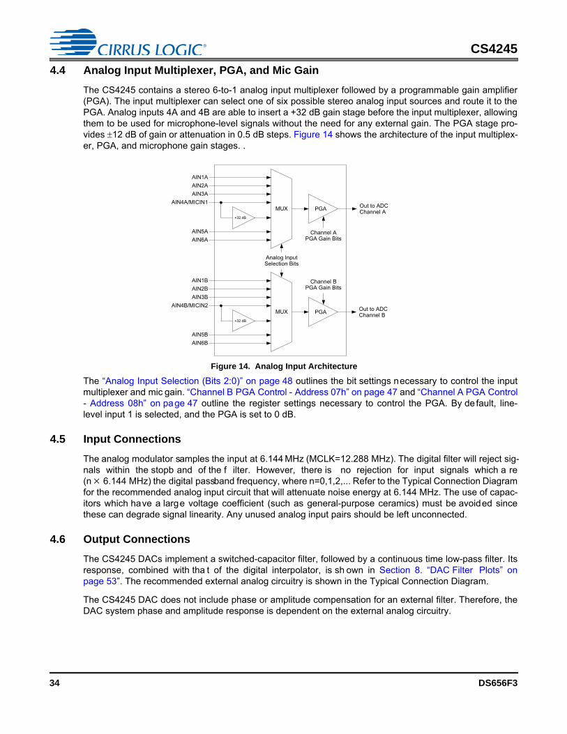
4.4 Analog Input Multiplexer, PGA, and Mic Gain
The CS4245 contains a stereo 6-to-1 analog input multiplexer followed by a programmable gain amplifier(PGA). The input multiplexer can select one of six possible stereo analog input sources and route it to thePGA. Analog inputs 4A and 4B are able to insert a +32 dB gain stage before the input multiplexer, allowingthem to be used for microphone-level signals without the need for any external gain. The PGA stage pro-vides 12 dB of gain or attenuation in 0.5 dB steps. Figure 14 shows the architecture of the input multiplex-er, PGA, and microphone gain stages. .
The “Analog Input Selection (Bits 2:0)” on page 48 outlines the bit settings necessary to control the inputmultiplexer and mic gain. “Channel B PGA Control - Address 07h” on page 47 and “Channel A PGA Control- Address 08h” on page 47 outline the register settings necessary to control the PGA. By de fault, line-level input 1 is selected, and the PGA is set to 0 dB.
4.5 Input Connections
The analog modulator samples the input at 6.144 MHz (MCLK=12.288 MHz). The digital filter will reject sig-nals within the stopb and of the f ilter. However, there is no rejection for input signals which a re(n 6.144 MHz) the digital passband frequency, where n=0,1,2,... Refer to the Typical Connection Diagramfor the recommended analog input circuit that will attenuate noise energy at 6.144 MHz. The use of capac-itors which have a large voltage coefficient (such as general-purpose ceramics) must be avoided sincethese can degrade signal linearity. Any unused analog input pairs should be left unconnected.
4.6 Output Connections
The CS4245 DACs implement a switched-capacitor filter, followed by a continuous time low-pass filter. Itsresponse, combined with tha t of the digital interpolator, is sh own in Section 8. “DAC Filter Plots” onpage 53”. The recommended external analog circuitry is shown in the Typical Connection Diagram.
The CS4245 DAC does not include phase or amplitude compensation for an external filter. Therefore, theDAC system phase and amplitude response is dependent on the external analog circuitry.
PGAMUX+32 dB
AIN1AAIN2AAIN3A
AIN4A/MICIN1
AIN5AAIN6A
PGAMUX+32 dB
AIN1BAIN2BAIN3B
AIN4B/MICIN2
AIN5BAIN6B
Analog InputSelection Bits
Channel APGA Gain Bits
Channel BPGA Gain Bits
Out to ADCChannel A
Out to ADCChannel B
Figure 14. Analog Input Architecture
34 DS656F3
CS4245
4.7 Output Transient Control
The CS4245 uses Popguard® technology to minimize the effects of output transients during power-up andpower-down. This technique eliminates the audio transients commonly produced by single-ended, single-supply converters when it is implemented with external DC-blocking capacitors connected in series with theaudio outputs. To make best use of this feature, it is necessary to understand its operation.
4.7.1 Power-Up
When the device is initially powered-up, the audio outputs AOUTA and AOUTB are clamped to VQ2, which is initially low. After the PDN bit is released (set to ‘0’), the DAC outputs begin to ramp with VQ2 towards the nominal quiescent voltage. This ramp takes approximately 200 ms to complete. The gradual voltage ramping allows time for the external DC-blocking capacitors to charge to VQ2, effectively blocking the quiescent DC voltage. Audio output will begin after approximately 2000 sample periods.
4.7.2 Power-Down
To prevent audio transients at power-down, the DC-blocking capacitors must fully discharge before turn-ing off the power. In order to do this, either the PDN bit should be set or the device should be reset about 250 ms before removing power. During this time, the voltage on VQ2 and the DAC outputs discharge gradually to GND. If power is removed before this 250 ms time period has passed, a transient will occur when the VA supply drops below that of VQ2. There is no minimum time for a power cycle; power may be re-applied at any time.
4.7.3 Serial Interface Clock Changes
When changing the DAC clock ratio or sample rate, it is recommended that zero data (or near zero data) be present on SDIN for at least 10 LRCK samples before the change is made. During the clocking change, the DAC outputs will always be in a zero data state. If non-zero serial audio input is present at the time of switching, a slight click or pop may be heard as the DAC output automatically goes to its zero data state.
4.8 Auxiliary Analog Output
The CS4245 includes an auxiliary analog output through the AUXOUT pins. These pins can be configuredto output the analog input to the ADC as se lected with the input MUX and gained or attenuated with thePGA, the analog output of the DAC, or alternatively they may be set to high-impedance. See “Section 6.6.1“Auxiliary Output Source Select (Bits 6:5)” on page 46” for information on configuring the auxiliary analogoutput.
The auxiliary analog output can source very little current. As current from the AUXOUT pins increases, dis-tortion will increase. For this reason, a high input impedance buffer must be used on the AUXOUT pins toachieve full performance. Refer to the table in “Auxiliary Output Analog Characteristics” on page 17 for ac-ceptable loading conditions.
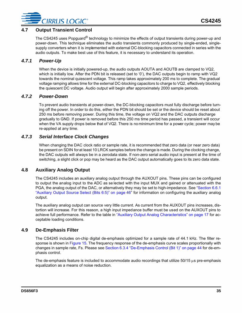
4.9 De-Emphasis Filter
The CS4245 includes on-chip digital de-emphasis optimized for a sample rate of 44.1 kHz. The filter re-sponse is shown in Figure 15. The frequency response of the de-emphasis curve scales proportionally withchanges in sample rate, Fs. Please see Section 6.3.4 “De-Emphasis Control (Bit 1)” on page 44 for de-em-phasis control.
The de-emphasis feature is included to accommodate audio recordings that utilize 50/15 s pre-emphasisequalization as a means of noise reduction.
DS656F3 35
CS4245
De-emphasis is only available in Single-Speed Mode.
4.10 Internal Digital Loopback
The CS4245 supports an internal digital loopback mode in which the output of the ADC is routed to the inputof the DAC. This mode may be activated by setting the LOOP bit in the Signal Selection register (See Sec-tion 6.6 “Signal Selection - Address 06h” on page 46). To use this mode, the ADC and DAC must be oper-ating at the same synchronous sample rate.
When this bit is set, the status of the DAC_DIF[1:0] bits in register 03h will be disregarded by the CS4245.Any changes made to the DAC_DIF[1:0] bits while the LOOP bit is set will have no impact on operation untilthe LOOP bit is cleared, at which time the Digital Interface Format of the DAC will operate according to theformat selected by the DAC_DIF[1:0] bits. While the LOOP bit is set, data will be present on the SDOUT pinin the format selected by the ADC_DIF bit in register 04h.
4.11 Mute Control
The MUTEC pin becomes active during power-up initialization, reset, and muting if the MCLK2 to LRCK2ratio is incorrect in Asynchronous Mode or the MCLK1 to LRCK2 ratio is incorrect in Synchronous Mode,and during power-down. The MUTEC pin is intended to be used as control for an external mute circuit inorder to add off-chip mute capability.
Use of the Mute Control function is not mandatory, but recommended, for designs requiring the absoluteminimum in extraneous clicks and pops. Also, use of the Mute Control function can enable the system de-
GaindB
-10dB
0dB
Frequency
T2 = 15 µs
T1=50 µs
F1 F23.183 kHz 10.61 kHz
Figure 15. De-Emphasis Curve
36 DS656F3
CS4245
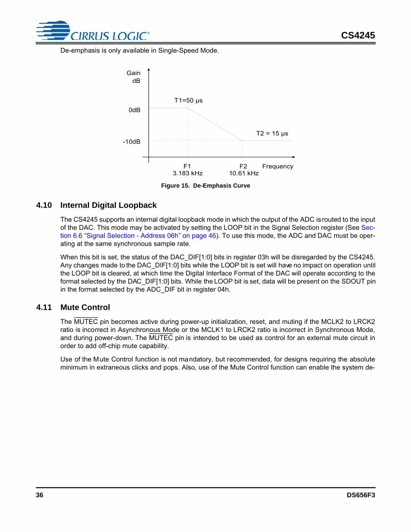
signer to achieve idle channel noise/signal-to-noise ratios which are only limited by the external mute circuit.The MUTEC pin is an active-low CMOS driver. See Figure 16 for a suggested active-low mute circuit.
4.12 Control Port Description and Timing
The control port is used to access the registers, allowing the CS4245 to be configured for the desired oper-ational modes and formats. The operation of the control port may be completely asynchronous with respectto the audio sample rates. However, to avoid potential interference problems, the control port pins shouldremain static if no operation is required.
The control port has two modes: SPI and I²C, with the CS4245 acting as a slave device. SPI Mode is se-lected if there is a high-to-low transition on the AD0/CS pin, after the RESET pin has been brought high. I²CMode is selected by connecting the AD0/CS pin through a resistor to VLC or DGND, thereby permanentlyselecting the desired AD0 bit address state.
4.12.1 SPI Mode
In SPI Mode, CS is the CS4245 chip-select signal; CCLK is the control port bit clock (input into the CS4245 from the microcontroller); CDIN is the input data line from the microcontroller; CDOUT is the output data line to the microcontroller. Data is clocked in on the rising edge of CCLK and out on the falling edge.
Figure 17 shows the operation of the control port in SPI Mode. To write to a register, bring CS low. The first seven bits on CDIN form the chip address and must be 1001111. The eighth bit is a read/write indi-cator (R/W), which should be low to write. The next eight bits form the Memory Address Pointer (MAP), which is set to the address of the register that is to be updated. The next eight bits are the data that will be placed into the register designated by the MAP. During writes, the CDOUT output stays in the Hi-Z state. It may be externally pulled high or low with a 47 k resistor, if desired.
To read a register, the MAP has to be set to the correct address by executing a partial write cycle which finishes (CS high) immediately after the MAP byte. To begin a read, bring CS low, send out the chip ad-
LPF
+VEE
-VEE
560 AudioOut
2 k
10 k
-VEE
+VA
MMUN2111LT1
AOUT
MUTEC
ACCouple
47 k
Figure 16. Suggested Active-Low Mute Circuit
CS4245
DS656F3 37
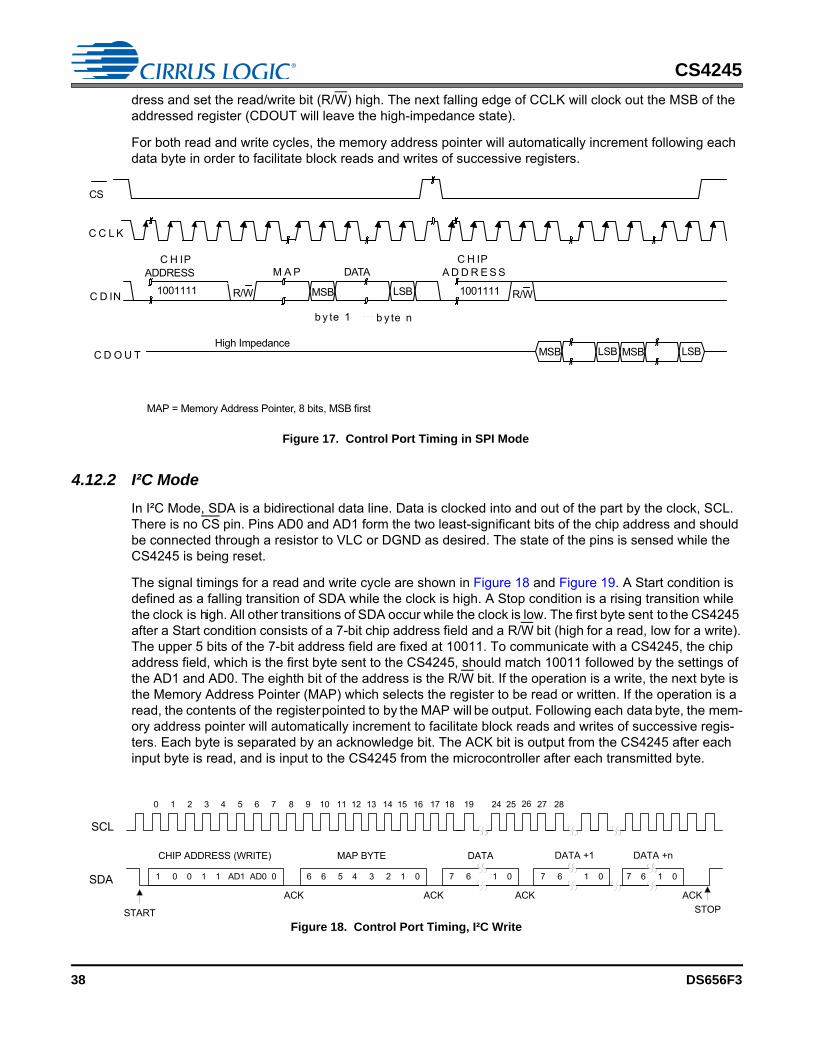
CS4245
dress and set the read/write bit (R/W) high. The next falling edge of CCLK will clock out the MSB of the addressed register (CDOUT will leave the high-impedance state).
For both read and write cycles, the memory address pointer will automatically increment following each data byte in order to facilitate block reads and writes of successive registers.
4.12.2 I²C Mode
In I²C Mode, SDA is a bidirectional data line. Data is clocked into and out of the part by the clock, SCL. There is no CS pin. Pins AD0 and AD1 form the two least-significant bits of the chip address and should be connected through a resistor to VLC or DGND as desired. The state of the pins is sensed while the CS4245 is being reset.
The signal timings for a read and write cycle are shown in Figure 18 and Figure 19. A Start condition is defined as a falling transition of SDA while the clock is high. A Stop condition is a rising transition while the clock is high. All other transitions of SDA occur while the clock is low. The first byte sent to the CS4245 after a Start condition consists of a 7-bit chip address field and a R/W bit (high for a read, low for a write). The upper 5 bits of the 7-bit address field are fixed at 10011. To communicate with a CS4245, the chip address field, which is the first byte sent to the CS4245, should match 10011 followed by the settings of the AD1 and AD0. The eighth bit of the address is the R/W bit. If the operation is a write, the next byte is the Memory Address Pointer (MAP) which selects the register to be read or written. If the operation is a read, the contents of the register pointed to by the MAP will be output. Following each data byte, the mem-ory address pointer will automatically increment to facilitate block reads and writes of successive regis-ters. Each byte is separated by an acknowledge bit. The ACK bit is output from the CS4245 after each input byte is read, and is input to the CS4245 from the microcontroller after each transmitted byte.
M A P
MSB LSB
DATA
b y te 1 b y te n
R/W R/W
A D D R E S SC H IP
ADDRESSC H IP
C D IN
C C L K
CS
C D O U T MSB LSB MSB LSB
10011111001111
MAP = Memory Address Pointer, 8 bits, MSB first
High Impedance
Figure 17. Control Port Timing in SPI Mode
4 5 6 7 24 25
SCL
CHIP ADDRESS (WRITE) MAP BYTE DATA DATA +1
START
ACKSTOP
ACKACKACK
1 0 0 1 1 AD1 AD0 0 SDA 6 6 5 4 3 2 1 0 7 6 1 0 7 6 1 0 7 6 1 0
0 1 2 3 8 9 12 16 17 18 19 10 11 13 14 15 27 2826
DATA +n
Figure 18. Control Port Timing, I²C Write
38 DS656F3
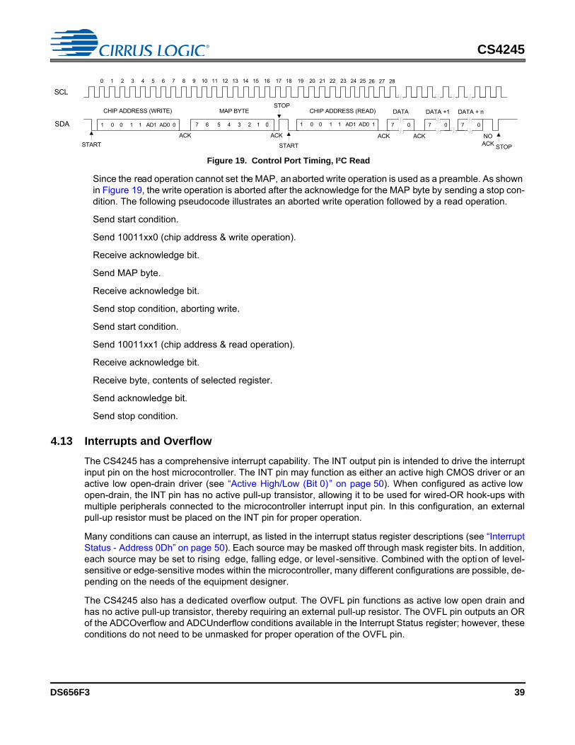
CS4245
Since the read operation cannot set the MAP, an aborted write operation is used as a preamble. As shown in Figure 19, the write operation is aborted after the acknowledge for the MAP byte by sending a stop con-dition. The following pseudocode illustrates an aborted write operation followed by a read operation.
Send start condition.
Send 10011xx0 (chip address & write operation).
Receive acknowledge bit.
Send MAP byte.
Receive acknowledge bit.
Send stop condition, aborting write.
Send start condition.
Send 10011xx1 (chip address & read operation).
Receive acknowledge bit.
Receive byte, contents of selected register.
Send acknowledge bit.
Send stop condition.
4.13 Interrupts and Overflow
The CS4245 has a comprehensive interrupt capability. The INT output pin is intended to drive the interruptinput pin on the host microcontroller. The INT pin may function as either an active high CMOS driver or anactive low open-drain driver (see “Active High/Low (Bit 0)” on page 50). When configured as active lowopen-drain, the INT pin has no active pull-up transistor, allowing it to be used for wired-OR hook-ups withmultiple peripherals connected to the microcontroller interrupt input pin. In this configuration, an externalpull-up resistor must be placed on the INT pin for proper operation.
Many conditions can cause an interrupt, as listed in the interrupt status register descriptions (see “InterruptStatus - Address 0Dh” on page 50). Each source may be masked off through mask register bits. In addition,each source may be set to rising edge, falling edge, or level -sensitive. Combined with the option of level-sensitive or edge-sensitive modes within the microcontroller, many different configurations are possible, de-pending on the needs of the equipment designer.
The CS4245 also has a dedicated overflow output. The OVFL pin functions as active low open drain andhas no active pull-up transistor, thereby requiring an external pull-up resistor. The OVFL pin outputs an ORof the ADCOverflow and ADCUnderflow conditions available in the Interrupt Status register; however, theseconditions do not need to be unmasked for proper operation of the OVFL pin.
SCL
CHIP ADDRESS (WRITE) MAP BYTE DATA DATA +1
STARTACK
STOPACKACKACK
1 0 0 1 1 AD1 AD0 0 SDA 1 0 0 1 1 AD1 AD0 1
CHIP ADDRESS (READ)
START
7 6 5 4 3 2 1 0 7 0 7 0 7 0
NO
16 8 9 12 13 14 15 4 5 6 7 0 1 20 21 22 23 24 26 27 28 2 3 10 11 17 18 19 25
ACK
DATA + nSTOP
Figure 19. Control Port Timing, I²C Read
DS656F3 39

CS4245
4.14 Reset
When RESET is low, the CS4245 enters a low-power mode and all internal states are reset, including thecontrol port and registers, the outputs are muted. When RESET is high, the control port becomes operation-al, and the desired settings should be loaded into the control registers. Writing a 0 to the PDN bit in the Pow-er Control register will then cause the part to leave the low-power state and begin operation.
The delta-sigma modulators settle in a matter of microseconds after the analog section is powered, eitherthrough the application of power or by setting the RESET pin high. However, the voltage reference will takemuch longer to reach a final value due to the presence of external capacitance on the FILT1+ and FILT2+pins. During this voltage reference ramp delay, both SDOUT and DAC outputs will be automatically muted.
It is recommended that RESET be activated if the analog or digital supplies drop below the recommendedoperating condition to prevent power-glitch-related issues.
4.15 Synchronization of Multiple Devices
In systems where multiple ADCs are required, care must be taken to achieve simultaneous sampling. Toensure synchronous sampling, the mast er clocks and left/ right clocks must be the same f or all of theCS4245s in the system. If only one master clock source is needed, one solution is to place one CS4245 inMaster Mode, and slave all of the other CS4245s to the one master. If multiple master clock sources areneeded, a possible solution would be to supply all clocks from the same external source and time theCS4245 reset with the inactive edge of master clock. This will ensure that all converters begin sampling onthe same clock edge.
4.16 Grounding and Power Supply Decoupling
As with any high-resolution converter, the CS4245 requires careful attention to power supply and groundingarrangements if its potential performance is to be realized. Figure 12 shows the recommended power ar-rangements, with VA connected to a clean supply. VD, which powers the digital filter, may be run from thesystem logic supply (VLS or VLC) or may be powered from the analog supply (VA) via a resistor. In thiscase, no additional devices should be powered from VD. Power supply decoupling capacitors should be asnear to the CS4245 as possible, with the low value ceramic capacitor being the nearest. All signals, espe-cially clocks, should be kept away from the FILT1+, FILT2+, VQ1 and VQ2 pins in order to avoid unwantedcoupling into the modulators. The FILT1+, FILT2+, VQ1 and VQ2 decoupling capacitors, particularly the0.1 µF, must be positioned to minimize the electrical path from FILT1+ and FILT2+ and AGND. The CS4245evaluation board demonstrates the optimum layout and power supply arrangements. To minimize digitalnoise, connect the CS4245 digital outputs only to CMOS inputs.
40 DS656F3
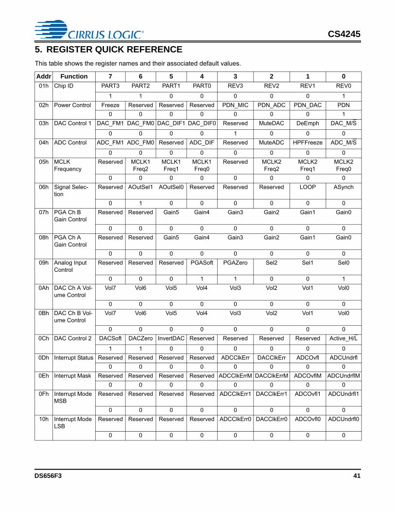
CS4245
5. REGISTER QUICK REFERENCE
This table shows the register names and their associated default values.
Addr Function 7 6 5 4 3 2 1 0
01h Chip ID PART3 PART2 PART1 PART0 REV3 REV2 REV1 REV0
1 1 0 0 0 0 0 102h Power Control Freeze Reserved Reserved Reserved PDN_MIC PDN_ADC PDN_DAC PDN
0 0 0 0 0 0 0 103h DAC Control 1 DAC_FM1 DAC_FM0 DAC_DIF1 DAC_DIF0 Reserved MuteDAC DeEmph DAC_M/S
0 0 0 0 1 0 0 004h ADC Control ADC_FM1 ADC_FM0 Reserved ADC_DIF Reserved MuteADC HPFFreeze ADC_M/S
0 0 0 0 0 0 0 005h MCLK
FrequencyReserved MCLK1
Freq2MCLK1Freq1
MCLK1Freq0
Reserved MCLK2Freq2
MCLK2Freq1
MCLK2Freq0
0 0 0 0 0 0 0 006h Signal Selec-
tionReserved AOutSel1 AOutSel0 Reserved Reserved Reserved LOOP ASynch
0 1 0 0 0 0 0 007h PGA Ch B
Gain ControlReserved Reserved Gain5 Gain4 Gain3 Gain2 Gain1 Gain0
0 0 0 0 0 0 0 008h PGA Ch A
Gain ControlReserved Reserved Gain5 Gain4 Gain3 Gain2 Gain1 Gain0
0 0 0 0 0 0 0 009h Analog Input
ControlReserved Reserved Reserved PGASoft PGAZero Sel2 Sel1 Sel0
0 0 0 1 1 0 0 10Ah DAC Ch A Vol-
ume ControlVol7 Vol6 Vol5 Vol4 Vol3 Vol2 Vol1 Vol0
0 0 0 0 0 0 0 00Bh DAC Ch B Vol-
ume ControlVol7 Vol6 Vol5 Vol4 Vol3 Vol2 Vol1 Vol0
0 0 0 0 0 0 0 00Ch DAC Control 2 DACSoft DACZero InvertDAC Reserved Reserved Reserved Reserved Active_H/L
1 1 0 0 0 0 0 00Dh Interrupt Status Reserved Reserved Reserved Reserved ADCClkErr DACClkErr ADCOvfl ADCUndrfl
0 0 0 0 0 0 0 00Eh Interrupt Mask Reserved Reserved Reserved Reserved ADCClkErrM DACClkErrM ADCOvflM ADCUndrflM
0 0 0 0 0 0 0 00Fh Interrupt Mode
MSBReserved Reserved Reserved Reserved ADCClkErr1 DACClkErr1 ADCOvfl1 ADCUndrfl1
0 0 0 0 0 0 0 010h Interrupt Mode
LSBReserved Reserved Reserved Reserved ADCClkErr0 DACClkErr0 ADCOvfl0 ADCUndrfl0
0 0 0 0 0 0 0 0
DS656F3 41
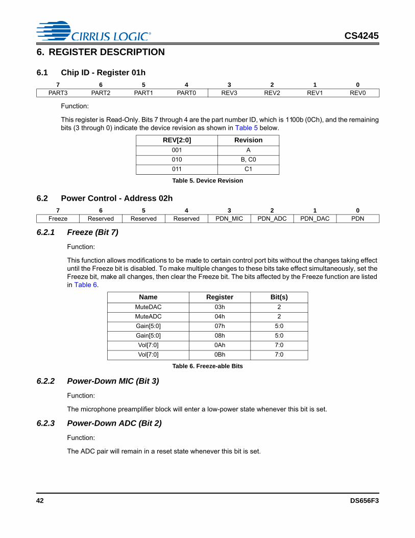
CS4245
6. REGISTER DESCRIPTION
6.1 Chip ID - Register 01h
Function:
This register is Read-Only. Bits 7 through 4 are the part number ID, which is 1100b (0Ch), and the remainingbits (3 through 0) indicate the device revision as shown in Table 5 below.
6.2 Power Control - Address 02h
6.2.1 Freeze (Bit 7)
Function:
This function allows modifications to be made to certain control port bits without the changes taking effect until the Freeze bit is disabled. To make multiple changes to these bits take effect simultaneously, set the Freeze bit, make all changes, then clear the Freeze bit. The bits affected by the Freeze function are listed in Table 6.
6.2.2 Power-Down MIC (Bit 3)
Function:
The microphone preamplifier block will enter a low-power state whenever this bit is set.
6.2.3 Power-Down ADC (Bit 2)
Function:
The ADC pair will remain in a reset state whenever this bit is set.
7 6 5 4 3 2 1 0PART3 PART2 PART1 PART0 REV3 REV2 REV1 REV0
REV[2:0] Revision
001 A010 B, C0011 C1
Table 5. Device Revision
7 6 5 4 3 2 1 0Freeze Reserved Reserved Reserved PDN_MIC PDN_ADC PDN_DAC PDN
Name Register Bit(s)
MuteDAC 03h 2MuteADC 04h 2Gain[5:0] 07h 5:0Gain[5:0] 08h 5:0Vol[7:0] 0Ah 7:0Vol[7:0] 0Bh 7:0
Table 6. Freeze-able Bits
42 DS656F3
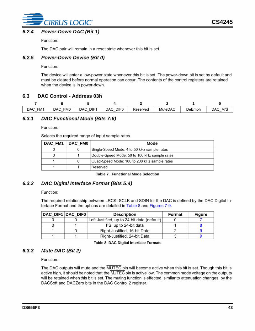
CS4245
6.2.4 Power-Down DAC (Bit 1)
Function:
The DAC pair will remain in a reset state whenever this bit is set.
6.2.5 Power-Down Device (Bit 0)
Function:
The device will enter a low-power state whenever this bit is set. The power-down bit is set by default and must be cleared before normal operation can occur. The contents of the control registers are retained when the device is in power-down.
6.3 DAC Control - Address 03h
6.3.1 DAC Functional Mode (Bits 7:6)
Function:
Selects the required range of input sample rates.
6.3.2 DAC Digital Interface Format (Bits 5:4)
Function:
The required relationship between LRCK, SCLK and SDIN for the DAC is defined by the DAC Digital In-terface Format and the options are detailed in Table 8 and Figures 7-9.
6.3.3 Mute DAC (Bit 2)
Function:
The DAC outputs will mute and the MUTEC pin will become active when this bit is set. Though this bit is active high, it should be noted that the MUTEC pin is active low. The common mode voltage on the outputs will be retained when this bit is set. The muting function is effected, similar to attenuation changes, by the DACSoft and DACZero bits in the DAC Control 2 register.
7 6 5 4 3 2 1 0
DAC_FM1 DAC_FM0 DAC_DIF1 DAC_DIF0 Reserved MuteDAC DeEmph DAC_M/S
DAC_FM1 DAC_FM0 Mode
0 0 Single-Speed Mode: 4 to 50 kHz sample rates0 1 Double-Speed Mode: 50 to 100 kHz sample rates1 0 Quad-Speed Mode: 100 to 200 kHz sample rates1 1 Reserved
Table 7. Functional Mode Selection
DAC_DIF1 DAC_DIF0 Description Format Figure0 0 Left Justified, up to 24-bit data (default) 0 70 1 I²S, up to 24-bit data 1 81 0 Right-Justified, 16-bit Data 2 91 1 Right-Justified, 24-bit Data 3 9
Table 8. DAC Digital Interface Formats
DS656F3 43
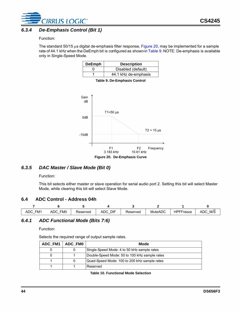
CS4245
6.3.4 De-Emphasis Control (Bit 1)
Function:
The standard 50/15 s digital de-emphasis filter response, Figure 20, may be implemented for a sample rate of 44.1 kHz when the DeEmph bit is configured as shown in Table 9. NOTE: De-emphasis is available only in Single-Speed Mode.
6.3.5 DAC Master / Slave Mode (Bit 0)
Function:
This bit selects either master or slave operation for serial audio port 2. Setting this bit will select Master Mode, while clearing this bit will select Slave Mode.
6.4 ADC Control - Address 04h
6.4.1 ADC Functional Mode (Bits 7:6)
Function:
Selects the required range of output sample rates.
DeEmph Description0 Disabled (default)1 44.1 kHz de-emphasis
Table 9. De-Emphasis Control
7 6 5 4 3 2 1 0
ADC_FM1 ADC_FM0 Reserved ADC_DIF Reserved MuteADC HPFFreeze ADC_M/S
ADC_FM1 ADC_FM0 Mode
0 0 Single-Speed Mode: 4 to 50 kHz sample rates0 1 Double-Speed Mode: 50 to 100 kHz sample rates1 0 Quad-Speed Mode: 100 to 200 kHz sample rates1 1 Reserved
Table 10. Functional Mode Selection
GaindB
-10dB
0dB
Frequency
T2 = 15 µs
T1=50 µs
F1 F23.183 kHz 10.61 kHz
Figure 20. De-Emphasis Curve
44 DS656F3
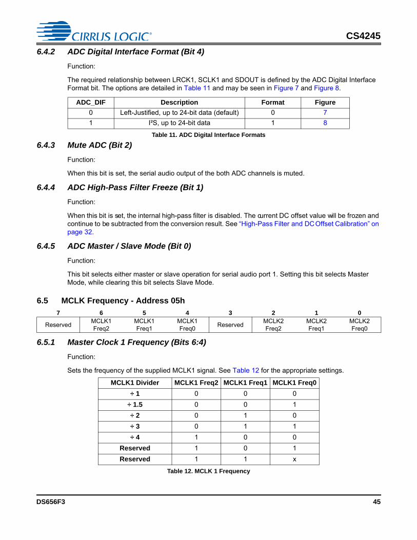
CS4245
6.4.2 ADC Digital Interface Format (Bit 4)
Function:
The required relationship between LRCK1, SCLK1 and SDOUT is defined by the ADC Digital Interface Format bit. The options are detailed in Table 11 and may be seen in Figure 7 and Figure 8.
6.4.3 Mute ADC (Bit 2)
Function:
When this bit is set, the serial audio output of the both ADC channels is muted.
6.4.4 ADC High-Pass Filter Freeze (Bit 1)
Function:
When this bit is set, the internal high-pass filter is disabled. The current DC offset value will be frozen and continue to be subtracted from the conversion result. See “High-Pass Filter and DC Offset Calibration” on page 32.
6.4.5 ADC Master / Slave Mode (Bit 0)
Function:
This bit selects either master or slave operation for serial audio port 1. Setting this bit selects Master Mode, while clearing this bit selects Slave Mode.
6.5 MCLK Frequency - Address 05h
6.5.1 Master Clock 1 Frequency (Bits 6:4)
Function:
Sets the frequency of the supplied MCLK1 signal. See Table 12 for the appropriate settings.
ADC_DIF Description Format Figure
0 Left-Justified, up to 24-bit data (default) 0 71 I²S, up to 24-bit data 1 8
Table 11. ADC Digital Interface Formats
7 6 5 4 3 2 1 0
Reserved MCLK1Freq2
MCLK1Freq1
MCLK1Freq0 Reserved MCLK2
Freq2MCLK2Freq1
MCLK2Freq0
MCLK1 Divider MCLK1 Freq2 MCLK1 Freq1 MCLK1 Freq0
÷ 1 0 0 0÷ 1.5 0 0 1÷ 2 0 1 0÷ 3 0 1 1÷ 4 1 0 0
Reserved 1 0 1Reserved 1 1 x
Table 12. MCLK 1 Frequency
DS656F3 45
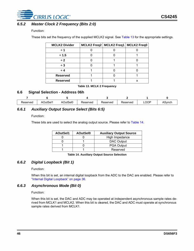
CS4245
6.5.2 Master Clock 2 Frequency (Bits 2:0)
Function:
These bits set the frequency of the supplied MCLK2 signal. See Table 13 for the appropriate settings.
6.6 Signal Selection - Address 06h
6.6.1 Auxiliary Output Source Select (Bits 6:5)
Function:
These bits are used to select the analog output source. Please refer to Table 14.
6.6.2 Digital Loopback (Bit 1)
Function:
When this bit is set, an internal digital loopback from the ADC to the DAC are enabled. Please refer to “Internal Digital Loopback” on page 36.
6.6.3 Asynchronous Mode (Bit 0)
Function:
When this bit is set, the DAC and ADC may be operated at independent asynchronous sample rates de-rived from MCLK1 and MCLK2. When this bit is cleared, the DAC and ADC must operate at synchronous sample rates derived from MCLK1.
MCLK2 Divider MCLK2 Freq2 MCLK2 Freq1 MCLK2 Freq0
÷ 1 0 0 0÷ 1.5 0 0 1÷ 2 0 1 0÷ 3 0 1 1÷ 4 1 0 0
Reserved 1 0 1Reserved 1 1 x
Table 13. MCLK 2 Frequency
7 6 5 4 3 2 1 0
Reserved AOutSel1 AOutSel0 Reserved Reserved Reserved LOOP ASynch
AOutSel1 AOutSel0 Auxiliary Output Source0 0 High Impedance0 1 DAC Output1 0 PGA Output1 1 Reserved
Table 14. Auxiliary Output Source Selection
46 DS656F3
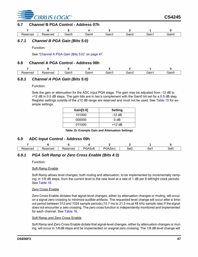
CS4245
6.7 Channel B PGA Control - Address 07h
6.7.1 Channel B PGA Gain (Bits 5:0)
Function:
See “Channel A PGA Gain (Bits 5:0)” on page 47.
6.8 Channel A PGA Control - Address 08h
6.8.1 Channel A PGA Gain (Bits 5:0)
Function:
Sets the gain or attenuation for the ADC input PGA stage. The gain may be adjusted from -12 dB to +12 dB in 0.5 dB steps. The gain bits are in two’s complement with the Gain0 bit set for a 0.5 dB step. Register settings outside of the ±12 dB range are reserved and must not be used. See Table 15 for ex-ample settings.
6.9 ADC Input Control - Address 09h
6.9.1 PGA Soft Ramp or Zero Cross Enable (Bits 4:3)
Function:
Soft Ramp Enable
Soft Ramp allows level changes, both muting and attenuation, to be implemented by incrementally ramp-ing, in 1/8 dB steps, from the current level to the new level at a rate of 1 dB per 8 left/right clock periods. See Table 16.
Zero Cross Enable
Zero Cross Enable dictates that signal-level changes, either by attenuation changes or muting, will occur on a signal zero crossing to minimize audible artifacts. The requested level change will occur after a time-out period between 512 and 1024 sample periods (10.7 ms to 21.3 ms at 48 kHz sample rate) if the signal does not encounter a zero crossing. The zero cross function is independently monitored and implemented for each channel. See Table 16.
Soft Ramp and Zero Cross Enable
Soft Ramp and Zero Cross Enable dictate that signal-level changes, either by attenuation changes or mut-ing, will occur in 1/8 dB steps and be implemented on a signal zero crossing. The 1/8 dB level change will
7 6 5 4 3 2 1 0Reserved Reserved Gain5 Gain4 Gain3 Gain2 Gain1 Gain0
7 6 5 4 3 2 1 0Reserved Reserved Gain5 Gain4 Gain3 Gain2 Gain1 Gain0
Gain[5:0] Setting
101000 -12 dB000000 0 dB011000 +12 dB
Table 15. Example Gain and Attenuation Settings
7 6 5 4 3 2 1 0Reserved Reserved Reserved PGASoft PGAZero Sel2 Sel1 Sel0
DS656F3 47
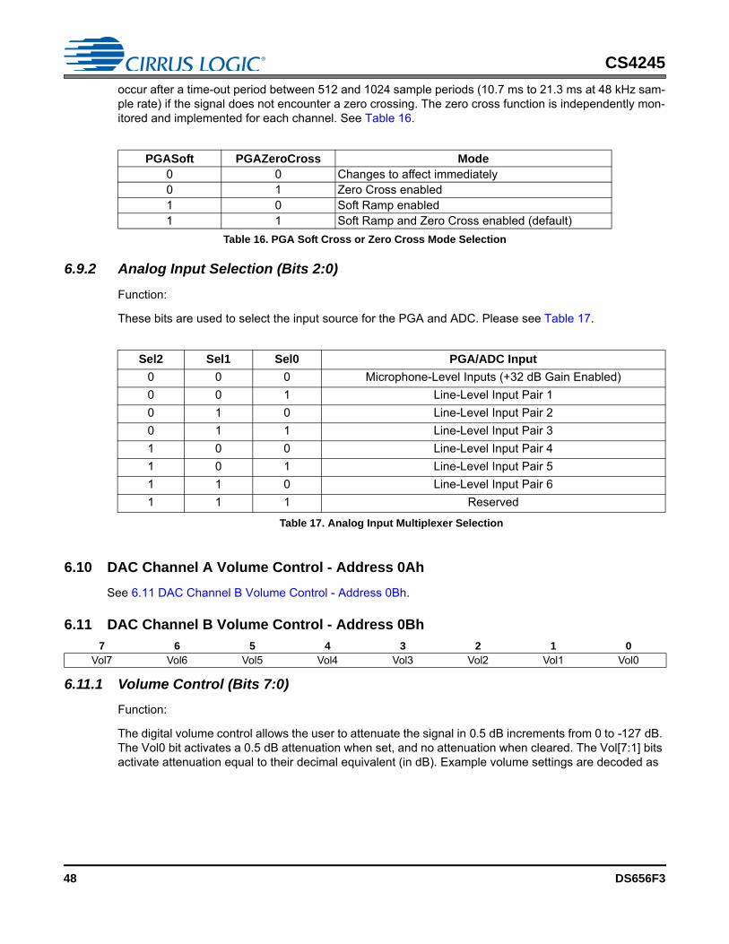
CS4245
occur after a time-out period between 512 and 1024 sample periods (10.7 ms to 21.3 ms at 48 kHz sam-ple rate) if the signal does not encounter a zero crossing. The zero cross function is independently mon-itored and implemented for each channel. See Table 16.
6.9.2 Analog Input Selection (Bits 2:0)
Function:
These bits are used to select the input source for the PGA and ADC. Please see Table 17.
6.10 DAC Channel A Volume Control - Address 0Ah
See 6.11 DAC Channel B Volume Control - Address 0Bh.
6.11 DAC Channel B Volume Control - Address 0Bh
6.11.1 Volume Control (Bits 7:0)
Function:
The digital volume control allows the user to attenuate the signal in 0.5 dB increments from 0 to -127 dB. The Vol0 bit activates a 0.5 dB attenuation when set, and no attenuation when cleared. The Vol[7:1] bits activate attenuation equal to their decimal equivalent (in dB). Example volume settings are decoded as
PGASoft PGAZeroCross Mode0 0 Changes to affect immediately0 1 Zero Cross enabled1 0 Soft Ramp enabled1 1 Soft Ramp and Zero Cross enabled (default)
Table 16. PGA Soft Cross or Zero Cross Mode Selection
Sel2 Sel1 Sel0 PGA/ADC Input
0 0 0 Microphone-Level Inputs (+32 dB Gain Enabled)0 0 1 Line-Level Input Pair 10 1 0 Line-Level Input Pair 20 1 1 Line-Level Input Pair 31 0 0 Line-Level Input Pair 41 0 1 Line-Level Input Pair 51 1 0 Line-Level Input Pair 61 1 1 Reserved
Table 17. Analog Input Multiplexer Selection
7 6 5 4 3 2 1 0Vol7 Vol6 Vol5 Vol4 Vol3 Vol2 Vol1 Vol0
48 DS656F3
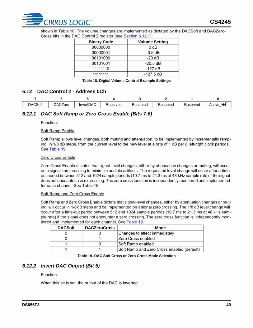
CS4245
shown in Table 18. The volume changes are implemented as dictated by the DACSoft and DACZero-Cross bits in the DAC Control 2 register (see Section 6.12.1).
6.12 DAC Control 2 - Address 0Ch
6.12.1 DAC Soft Ramp or Zero Cross Enable (Bits 7:6)
Function:
Soft Ramp Enable
Soft Ramp allows level changes, both muting and attenuation, to be implemented by incrementally ramp-ing, in 1/8 dB steps, from the current level to the new level at a rate of 1 dB per 8 left/right clock periods. See Table 19.
Zero Cross Enable
Zero Cross Enable dictates that signal-level changes, either by attenuation changes or muting, will occur on a signal zero crossing to minimize audible artifacts. The requested level change will occur after a time-out period between 512 and 1024 sample periods (10.7 ms to 21.3 ms at 48 kHz sample rate) if the signal does not encounter a zero crossing. The zero cross function is independently monitored and implemented for each channel. See Table 19.
Soft Ramp and Zero Cross Enable
Soft Ramp and Zero Cross Enable dictate that signal-level changes, either by attenuation changes or mut-ing, will occur in 1/8 dB steps and be implemented on a signal zero crossing. The 1/8 dB level change will occur after a time-out period between 512 and 1024 sample periods (10.7 ms to 21.3 ms at 48 kHz sam-ple rate) if the signal does not encounter a zero crossing. The zero cross function is independently mon-itored and implemented for each channel. See Table 19.
6.12.2 Invert DAC Output (Bit 5)
Function:
When this bit is set, the output of the DAC is inverted.
Binary Code Volume Setting00000000 0 dB00000001 -0.5 dB00101000 -20 dB00101001 -20.5 dB11111110 -127 dB11111111 -127.5 dB
Table 18. Digital Volume Control Example Settings
7 6 5 4 3 2 1 0
DACSoft DACZero InvertDAC Reserved Reserved Reserved Reserved Active_H/L
DACSoft DACZeroCross Mode0 0 Changes to affect immediately0 1 Zero Cross enabled1 0 Soft Ramp enabled1 1 Soft Ramp and Zero Cross enabled (default)
Table 19. DAC Soft Cross or Zero Cross Mode Selection
DS656F3 49
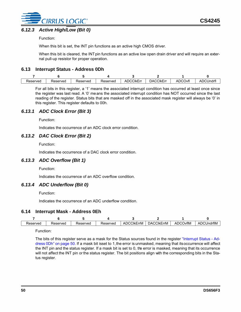
CS4245
6.12.3 Active High/Low (Bit 0)
Function:
When this bit is set, the INT pin functions as an active high CMOS driver.
When this bit is cleared, the INT pin functions as an active low open drain driver and will require an exter-nal pull-up resistor for proper operation.
6.13 Interrupt Status - Address 0Dh
For all bits in this register, a ‘1’ means the associated interrupt condition has occurred at least once sincethe register was last read. A ‘0’ means the associated interrupt condition has NOT occurred since the lastreading of the register. Status bits that are masked off in the associated mask register will always be ‘0’ inthis register. This register defaults to 00h.
6.13.1 ADC Clock Error (Bit 3)
Function:
Indicates the occurrence of an ADC clock error condition.
6.13.2 DAC Clock Error (Bit 2)
Function:
Indicates the occurrence of a DAC clock error condition.
6.13.3 ADC Overflow (Bit 1)
Function:
Indicates the occurrence of an ADC overflow condition.
6.13.4 ADC Underflow (Bit 0)
Function:
Indicates the occurrence of an ADC underflow condition.
6.14 Interrupt Mask - Address 0Eh
Function:
The bits of this register serve as a mask for the Status sources found in the register “Interrupt Status - Ad-dress 0Dh” on page 50. If a mask bit is set to 1, the error is unmasked, meaning that its occurrence will affectthe INT pin and the status register. If a mask bit is set to 0, the error is masked, meaning that its occurrencewill not affect the INT pin or the status register. The bit positions align with the corresponding bits in the Sta-tus register.
7 6 5 4 3 2 1 0Reserved Reserved Reserved Reserved ADCClkErr DACClkErr ADCOvfl ADCUndrfl
7 6 5 4 3 2 1 0Reserved Reserved Reserved Reserved ADCClkErrM DACClkErrM ADCOvflM ADCUndrflM
50 DS656F3
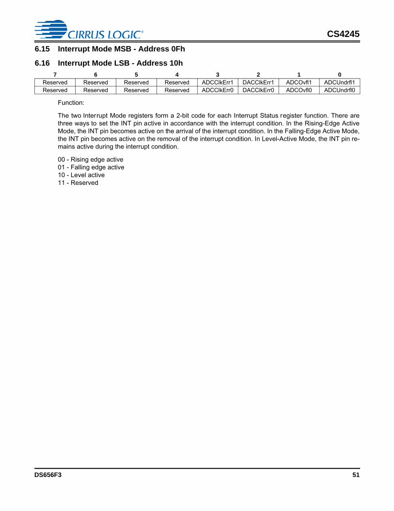
CS4245
6.15 Interrupt Mode MSB - Address 0Fh
6.16 Interrupt Mode LSB - Address 10h
Function:
The two Interrupt Mode registers form a 2-bit code for each Interrupt Status register function. There arethree ways to set the INT pin active in accordance with the interrupt condition. In the Rising-Edge ActiveMode, the INT pin becomes active on the arrival of the interrupt condition. In the Falling-Edge Active Mode,the INT pin becomes active on the removal of the interrupt condition. In Level-Active Mode, the INT pin re-mains active during the interrupt condition.
00 - Rising edge active01 - Falling edge active10 - Level active11 - Reserved
7 6 5 4 3 2 1 0Reserved Reserved Reserved Reserved ADCClkErr1 DACClkErr1 ADCOvfl1 ADCUndrfl1Reserved Reserved Reserved Reserved ADCClkErr0 DACClkErr0 ADCOvfl0 ADCUndrfl0
DS656F3 51
CS4245
7. PARAMETER DEFINITIONS
Dynamic Range
The ratio of the rms value of the signal to the rms sum of all other spectral components over the specifiedbandwidth. Dynamic Range is a signal-to-noise ratio measurement over the specified bandwidth made witha -60 dBFS signal. 60 dB is added to resulting measurement to refer the measurement to full scale. Thistechnique ensures that the distortion components are below the noise level and do not affect the measure-ment. This measurement technique has been accepted by the Au dio Engineering Society, AES17-1991,and the Electronic Industries Association of Japan, EIAJ CP-307. Expressed in decibels.
Total Harmonic Distortion + Noise
The ratio of the rms value of the signal to the rms sum of all other spectral components over the specifiedbandwidth (typically 10 Hz to 20 kHz), including distortion components. Expressed in decibels. Measuredat -1 and -20 dBFS as suggested in AES17-1991 Annex A.
Frequency Response
A measure of the amplitude response variation from 10 Hz to 20 kHz relative to the amplitude response at1 kHz. Units in decibels.
Interchannel Isolation
A measure of crosstalk between the left and right channels. Measured for each channel at the converter'soutput with no signal to the input under test and a full-scale signal applied to the other channel. Units in deci-bels.
Interchannel Gain Mismatch
The gain difference between left and right channels. Units in decibels.
Gain Drift
The change in gain value with temperature. Units in ppm/°C.
52 DS656F3
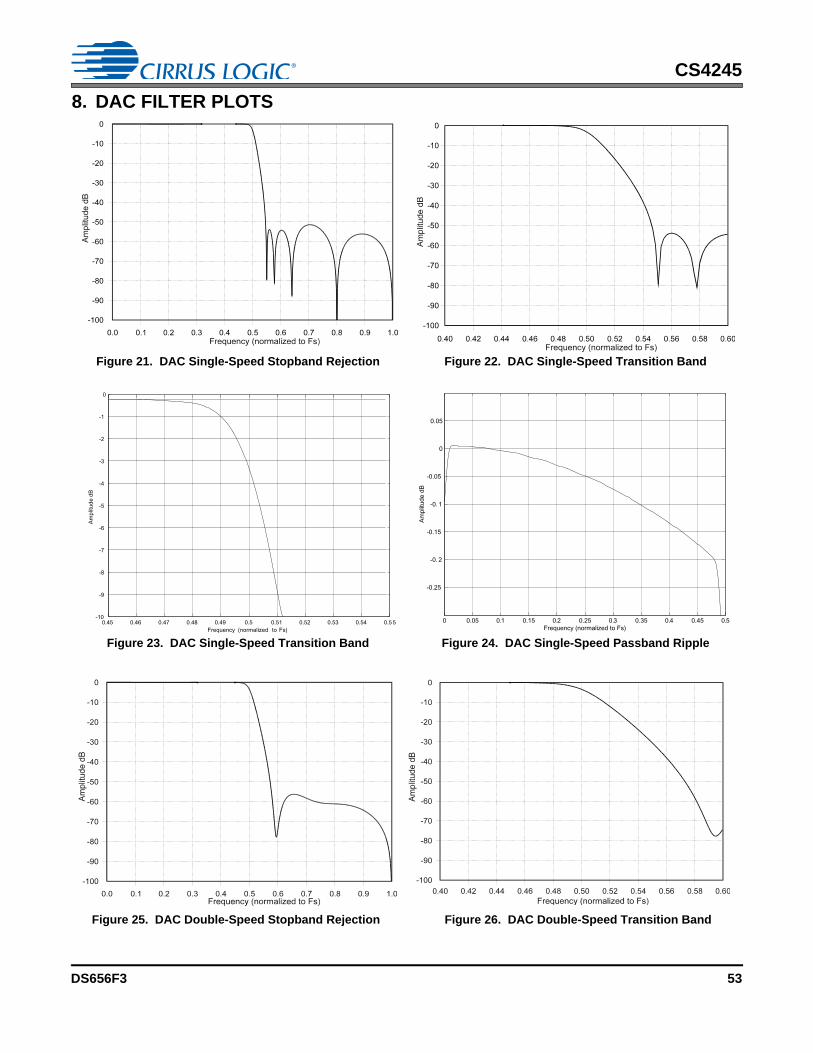
CS4245
8. DAC FILTER PLOTS
Figure 21. DAC Single-Speed Stopband Rejection Figure 22. DAC Single-Speed Transition Band
0 0.05 0.1 0.15 0.2 0.25 0.3 0.35 0.4 0.45 0.5
-0.25
-0. 2
-0.15
-0. 1
-0.05
0
0.05
Frequency (normalized to Fs)
Am
plitu
dedB
Figure 23. DAC Single-Speed Transition Band Figure 24. DAC Single-Speed Passband Ripple
0.45 0.46 0.47 0.48 0.49 0.5 0.51 0.52 0.53 0.54 0.5 5-10
-9
-8
-7
-6
-5
-4
-3
-2
-1
0
Frequency (normalized to Fs)
Am
plitu
dedB
Figure 25. DAC Double-Speed Stopband Rejection Figure 26. DAC Double-Speed Transition Band
DS656F3 53
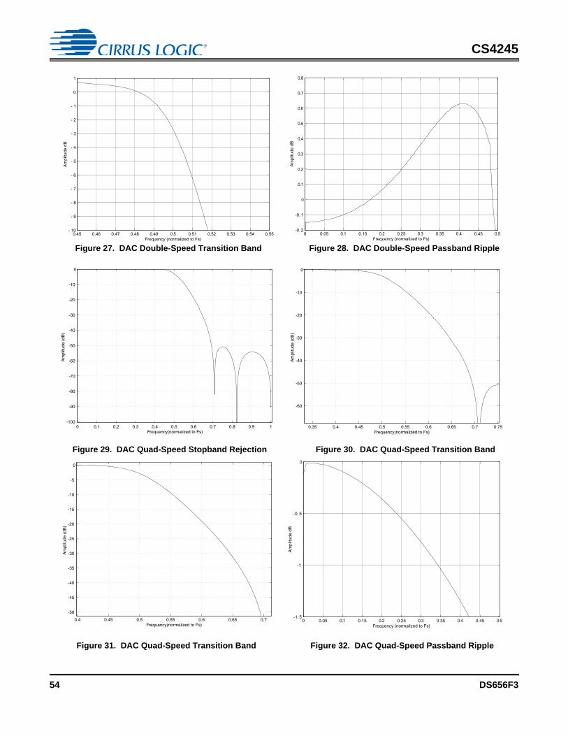
CS4245
0 0.05 0.1 0.15 0.2 0.25 0.3 0.35 0.4 0.45 0.5-0. 2
-0. 1
0
0.1
0.2
0.3
0.4
0.5
0.6
0.7
0.8
Frequency (normalized to Fs)
Am
plitu
dedB
0.45 0.46 0.47 0.48 0.49 0.5 0.51 0.52 0.53 0.54 0.55- 10
- 9
- 8
- 7
- 6
- 5
- 4
- 3
- 2
- 1
0
1
Frequency (normalized to Fs)
Am
plitu
dedB
Figure 27. DAC Double-Speed Transition Band Figure 28. DAC Double-Speed Passband Ripple
Figure 29. DAC Quad-Speed Stopband Rejection Figure 30. DAC Quad-Speed Transition Band
0.35 0.4 0.45 0.5 0.55 0.6 0.65 0.7 0.75
-60
-50
-40
-30
-20
-10
0
Am
plitu
de (
dB)
Frequency(normalized to Fs)0 0.1 0.2 0.3 0.4 0.5 0.6 0.7 0.8 0.9 1
-100
-90
-80
-70
-60
-50
-40
-30
-20
-10
0
Am
plitu
de (
dB)
Frequency(normalized to Fs)
0 0.05 0.1 0.15 0.2 0.25 0.3 0.35 0.4 0.45 0.5-1. 5
-1
-0. 5
0
Frequency (normalized to Fs)
Am
plitu
dedB
Figure 31. DAC Quad-Speed Transition Band Figure 32. DAC Quad-Speed Passband Ripple
0.4 0.45 0.5 0.55 0.6 0.65 0.7
-50
-45
-40
-35
-30
-25
-20
-15
-10
-5
0
Am
plitu
de (
dB)
Frequency(normalized to Fs)
54 DS656F3
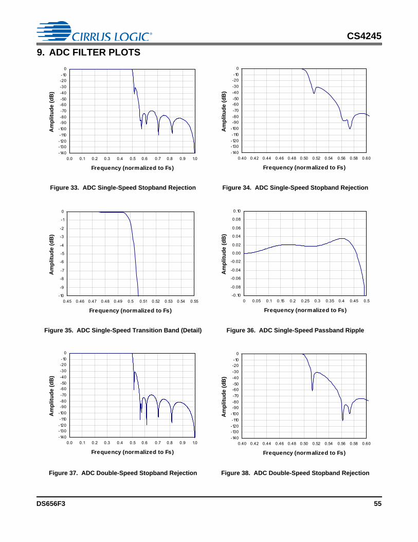
CS4245
9. ADC FILTER PLOTS
Figure 33. ADC Single-Speed Stopband Rejection Figure 34. ADC Single-Speed Stopband Rejection
Figure 35. ADC Single-Speed Transition Band (Detail) Figure 36. ADC Single-Speed Passband Ripple
Figure 37. ADC Double-Speed Stopband Rejection Figure 38. ADC Double-Speed Stopband Rejection
-140-130-120-110-100-90-80-70-60-50-40-30-20-10
0
0.0 0.1 0.2 0.3 0.4 0.5 0.6 0.7 0.8 0.9 1.0
Frequency (normalized to Fs)
Am
plit
ud
e (d
B)
-140-130-120-110-100-90-80-70-60-50-40-30-20-10
0
0.40 0.42 0.44 0.46 0.48 0.50 0.52 0.54 0.56 0.58 0.60
Frequency (normalized to Fs)
Am
plit
ud
e (d
B)
-10
-9
-8
-7
-6
-5
-4
-3
-2
-1
0
0.45 0.46 0.47 0.48 0.49 0.5 0.51 0.52 0.53 0.54 0.55
Frequency (normalized to Fs)
Am
plit
ud
e (d
B)
-0.10
-0.08
-0.06
-0.04
-0.02
0.00
0.02
0.04
0.06
0.08
0.10
0 0.05 0.1 0.15 0.2 0.25 0.3 0.35 0.4 0.45 0.5
Frequency (normalized to Fs)
Am
plit
ud
e (d
B)
-140-130-120-110-100-90-80-70-60-50-40-30-20-10
0
0.0 0.1 0.2 0.3 0.4 0.5 0.6 0.7 0.8 0.9 1.0
Frequency (normalized to Fs)
Am
plit
ud
e (d
B)
-140-130-120-110-100-90-80-70-60-50-40-30-20-10
0
0.40 0.42 0.44 0.46 0.48 0.50 0.52 0.54 0.56 0.58 0.60
Frequency (normalized to Fs)
Am
plit
ud
e (d
B)
DS656F3 55
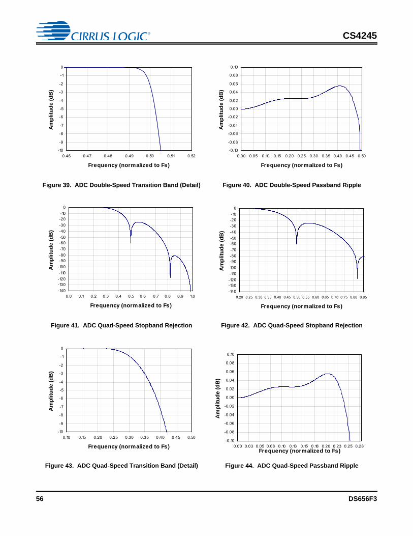
CS4245
Figure 39. ADC Double-Speed Transition Band (Detail) Figure 40. ADC Double-Speed Passband Ripple
Figure 41. ADC Quad-Speed Stopband Rejection Figure 42. ADC Quad-Speed Stopband Rejection
Figure 43. ADC Quad-Speed Transition Band (Detail) Figure 44. ADC Quad-Speed Passband Ripple
-10
-9
-8
-7
-6
-5
-4
-3
-2
-1
0
0.46 0.47 0.48 0.49 0.50 0.51 0.52
Frequency (normalized to Fs)
Am
plit
ud
e (d
B)
-0.10
-0.08
-0.06
-0.04
-0.02
0.00
0.02
0.04
0.06
0.08
0.10
0.00 0.05 0.10 0.15 0.20 0.25 0.30 0.35 0.40 0.45 0.50
Frequency (normalized to Fs)
Am
plit
ud
e (d
B)
-140-130-120-110-100-90-80-70-60-50-40-30-20-10
0
0.0 0.1 0.2 0.3 0.4 0.5 0.6 0.7 0.8 0.9 1.0
Frequency (normalized to Fs)
Am
plit
ud
e (d
B)
-140-130-120-110-100-90-80-70-60-50-40-30-20-10
0
0.20 0.25 0.30 0.35 0.40 0.45 0.50 0.55 0.60 0.65 0.70 0.75 0.80 0.85
Frequency (normalized to Fs)
Am
plit
ud
e (d
B)
-10
-9
-8
-7
-6
-5
-4
-3
-2
-1
0
0.10 0.15 0.20 0.25 0.30 0.35 0.40 0.45 0.50
Frequency (normalized to Fs)
Am
plit
ud
e (d
B)
-0.10
-0.08
-0.06
-0.04
-0.02
0.00
0.02
0.04
0.06
0.08
0.10
0.00 0.03 0.05 0.08 0.10 0.13 0.15 0.18 0.20 0.23 0.25 0.28Frequency (normalized to Fs)
Am
plit
ud
e (d
B)
56 DS656F3
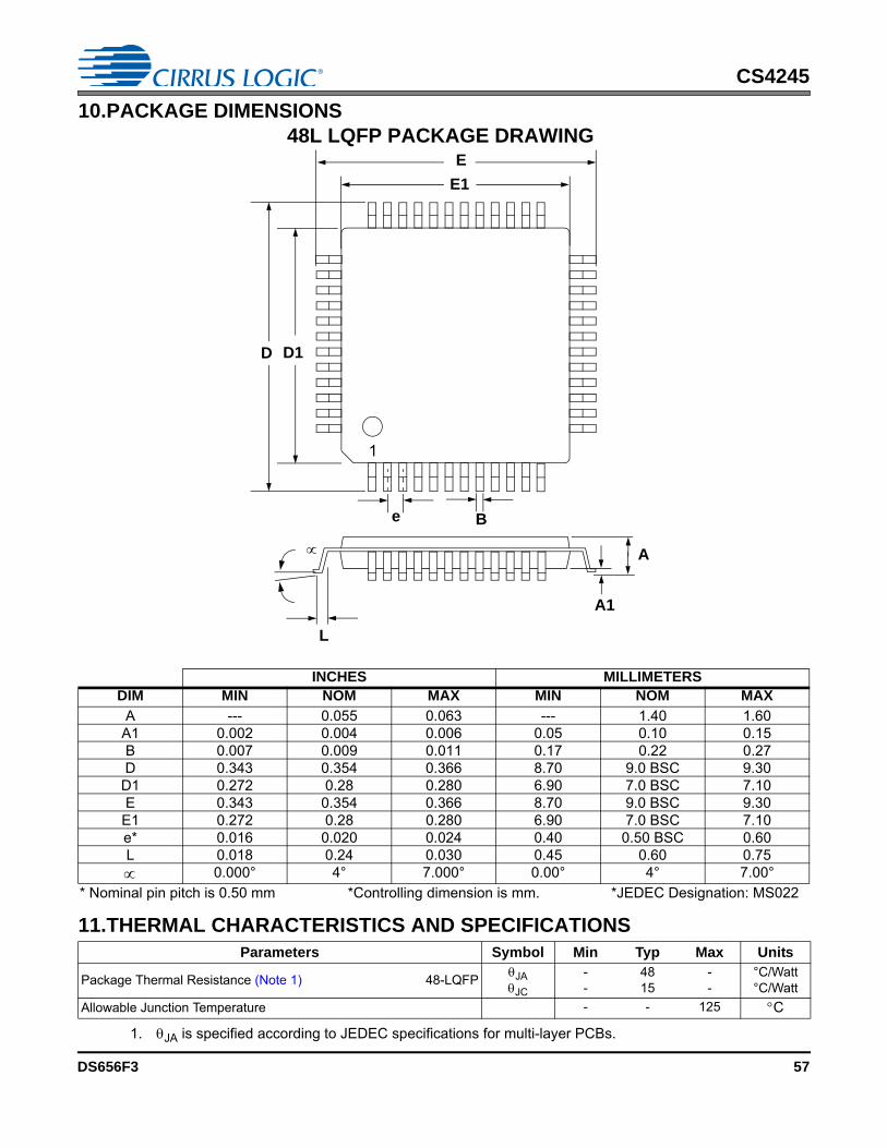
CS4245
10.PACKAGE DIMENSIONS
11.THERMAL CHARACTERISTICS AND SPECIFICATIONS
1. JA is specified according to JEDEC specifications for multi-layer PCBs.
INCHES MILLIMETERSDIM MIN NOM MAX MIN NOM MAX
A --- 0.055 0.063 --- 1.40 1.60A1 0.002 0.004 0.006 0.05 0.10 0.15B 0.007 0.009 0.011 0.17 0.22 0.27D 0.343 0.354 0.366 8.70 9.0 BSC 9.30
D1 0.272 0.28 0.280 6.90 7.0 BSC 7.10E 0.343 0.354 0.366 8.70 9.0 BSC 9.30E1 0.272 0.28 0.280 6.90 7.0 BSC 7.10e* 0.016 0.020 0.024 0.40 0.50 BSC 0.60L 0.018 0.24 0.030 0.45 0.60 0.75 0.000° 4° 7.000° 0.00° 4° 7.00°
* Nominal pin pitch is 0.50 mm *Controlling dimension is mm. *JEDEC Designation: MS022
Parameters Symbol Min Typ Max Units
Package Thermal Resistance (Note 1) 48-LQFP JAJC
--
4815
--
°C/Watt°C/Watt
Allowable Junction Temperature - - 125 C
48L LQFP PACKAGE DRAWING
E1
E
D1D
1
e
L
B
A1
A
DS656F3 57
CS4245
12.ORDERING INFORMATION
13.REVISION HISTORY
Product Description Package Pb-Free Grade Temp Range Container Order #
CS4245 24-bit, 192 kHz Stereo Audio CODEC 48-LQFP Yes Commercial -10° to +70° C
Tray CS4245-CQZTape & Reel CS4245-CQZR
CS4245 24-bit, 192 kHz Stereo Audio CODEC 48-LQFP Yes Automotive -40° to +105° C
Tray CS4245-DQZTape & Reel CS4245-DQZR
CDB4245 CS4245 Evaluation Board No - - - CDB4245
Release Changes
F1
– Removed the MAP auto-increment functional description from the Control Port Description and Timing section beginning on page 37.
– Added device revision information to the Chip ID - Register 01h description on page 42.– Updated the VQ1 Output Impedance specification in the DC Electrical Characteristics table on page 20.– Updated the Microphone Interchannel Isolation specification in the ADC Analog Characteristics table on page 15.
F2
– Added Automotive Grade– Changed MCLK1 and MCLK2 to input only in the Pin Descriptions table on page 7.– Updated the DAC Analog Characteristics table on page 10.– Updated the ADC Analog Characteristics table on page 13.– Updated the Auxiliary Output Analog Characteristics table on page 17.– Updated the DC Electrical Characteristics table on page 20.– Updated the Digital Interface Characteristics table on page 21.– Updated the Switching Characteristics - Serial Audio Port 1 table on page 22.– Updated the Switching Characteristics - Control Port - SPI Format table on page 28.– Updated the Typical Connection Diagram on page 29.– Switched Channel B PGA Control - Address 07h on page 47 and Channel A PGA Control - Address 08h on
page 47.F3 – Added Table 3.
58 DS656F3
CS4245
Contacting Cirrus Logic SupportFor all product questions and inquiries, contact a Cirrus Logic Sales Representative. To find the one nearest you, go to www.cirrus.com
IMPORTANT NOTICE
Cirrus Logic, Inc. and its subsidiaries (“Cirrus”) believe that the information contained in this document is accurate and reliable. However, the information is subjectto change without notice and is provided “AS IS” without warranty of any kind (express or implied). Customers are advised to obtain the latest version of relevantinformation to verify, before placing orders, that information being relied on is current and complete. All products are sold subject to the terms and conditions of salesupplied at the time of order acknowledgment, including those pertaining to warranty, indemnification, and limitation of liability. No responsibility is assumed by Cirrusfor the use of this information, including use of this information as the basis for manufacture or sale of any items, or for infringement of patents or other rights of thirdparties. This document is the property of Cirrus and by furnishing this information, Cirrus grants no license, express or implied under any patents, mask work rights,copyrights, trademarks, trade secrets or other intellectual property rights. Cirrus owns the copyrights associated with the information contained herein and gives con-sent for copies to be made of the information only for use within your organization with respect to Cirrus integrated circuits or other products of Cirrus. This consentdoes not extend to other copying such as copying for general distribution, advertising or promotional purposes, or for creating any work for resale. CERTAIN APPLICATIONS USING SEMICONDUCTOR PRODUCTS MAY INVOLVE POTENTIAL RISKS OF DEATH, PERSONAL INJURY, OR SEVERE PROP-ERTY OR ENVIRONMENTAL DAMAGE (“CRITICAL APPLICATIONS”). CIRRUS PRODUCTS ARE NOT DESIGNED, AUTHORIZED OR WARRANTED FOR USEIN AIRCRAFT SYSTEMS, MILITARY APPLICATIONS, PRODUCTS SURGICALLY IMPLANTED INTO THE BODY, AUTOMOTIVE SAFETY OR SECURITY DE-VICES, LIFE SUPPORT PRODUCTS OR OTHER CRITICAL APPLICATIONS. INCLUSION OF CIRRUS PRODUCTS IN SUCH APPLICATIONS IS UNDERSTOODTO BE FULLY AT THE CUSTOMER’S RISK AND CIRRUS DISCLAIMS AND MAKES NO WARRANTY, EXPRESS, STATUTORY OR IMPLIED, INCLUDING THEIMPLIED WARRANTIES OF MERCHANTABILITY AND FITNESS FOR PARTICULAR PURPOSE, WITH REGARD TO ANY CIRRUS PRODUCT THAT IS USEDIN SUCH A MANNER. IF THE CUSTOMER OR CUSTOMER’S CUSTOMER USES OR PERMITS THE USE OF CIRRUS PRODUCTS IN CRITICAL APPLICA-TIONS, CUSTOMER AGREES, BY SUCH USE, TO FULLY INDEMNIFY CIRRUS, ITS OFFICERS, DIRECTORS, EMPLOYEES, DISTRIBUTORS AND OTHERAGENTS FROM ANY AND ALL LIABILITY, INCLUDING ATTORNEYS’ FEES AND COSTS, THAT MAY RESULT FROM OR ARISE IN CONNECTION WITHTHESE USES.Cirrus Logic, Cirrus, the Cirrus Logic logo designs, and Popguard are trademarks of Cirrus Logic, Inc. All other brand and product names in this document may betrademarks or service marks of their respective owners.I²C is a registered trademark of Philips Semiconductor.SPI is a trademark of Motorola, Inc.
DS656F3 59