Embed Size (px)
Citation preview

DATASHEETPORTABLE CONSUMER CODECLOW-POWER, HIGH-FIDELITY INTEGRATED CODEC
TSCS42XX
TSI™ CONFIDENTIAL 1 V 0.5 2/16
©2014 TEMPO SEMICONDCUTOR, INC. TSCS42XX
DESCRIPTION
The TSCS42XX is a low-power, high-fidelity integrated CODEC with 32 bit stereo playback stereo record functionality. In addition to a high-fidelity low-power CODEC, the device integrates the true cap-less headphone amplifier.
The digital audio data format (I2S) works in master or slave mode and supports all I2S formats as well as direct Bluetooth PCM mode.
Beyond high-fidelity for portable systems, the device offers an enriched “audio presence” through built-in audio output processing DSP engine (AOP). The AOP supports 12 Bands of EQ, Psychoacoustic Bass and Treble enhancement, 3D stereo enhancement and Dynamic Range controller to support Multi-band Compressor/Limiter capability.
APPLICATIONS
• Bluetooth Speakers
• Portable Navigation Devices
• Portable Gaming Devices
• Personal Media Players
• Multimedia handsets
• E-books
• Chromebook /Tablets
FEATURES
• High fidelity CODEC • 2 DAC 102dB SNR• 2 ADC 90dB SNR• 32 bit stereo DAC and 32-bit stereo ADC• Sample rates of 8k to 96 kHz
• Audio Output Processing DSP Engine• 3D stereo enhancement• 12 band parametric equalizers• Dynamic Range controller
- Multi-band compressor - Limiter - Expander
• Psychoacoustic Bass and Treble enhancement processing
• 3rd Party algorithms
• DDX™ Digital Speaker Driver• 3W/channel 4Ω (1.5W/8Ω)• TSI DDX™ class D technology achieves low EMI and• high efficiency• >90% efficiency• Spread spectrum support for reduced EMI• Constant output power mode• Anti-Pop circuitry• Filterless architecture reduces BOM cost
• On-chip true cap-less headphone driver• 35 mW output power (16Ω)• Charge-pump allows true ground centered outputs• SNR (A-Weighted, no active signal) -122dB • SNR (A-Weighted, -60db active signal) -102dB• Headphone detection logic
• Microphone/line-in interface• Analog microphone or line-in inputs• Automatic level control• 1 stereo DMIC
• Low power with built in power management• 1.7 V CODEC supports 1Vrms• Very low standby and no-signal power consumption• 1.8V digital / 1.7V analog supply for low power
• 2-wire (I2C compatible) control interface
• I2S data interface• Supports Bluetooth mode• Left-Justified, Right-Justified and PCM Audio Interfaces
• package option • 5x5 QFN• 7x7 QFN
PLLInterna
lAudio Clocks
MUX
MUX
LIN1
LIN2
RIN1
RIN2
I2S /PCM
MICBIAS1
DAC
ChargePump
SPK Out L
I2C
XTAL/CLK IN
ADC
ADC
VREF
HP Detect
RIN3/DMIC D
HP/Line Out
HP/Line Out R
Class D
PWM
BTL
DAC
BTL
SPK Out R
(Cap-less)
GPIO’s
I2S /PCM OUT
(Cap-less)
XTAL OUT
MCLK
DSP
DSP
INPUT
PROCESSOR
+
- D2S
MUX
MUX
LIN1
LIN2
RIN1
RIN2
D2S
D2S MUX
D2S
LIN3/ DMIC C
TSI™ CONFIDENTIAL 2 V 0.95
©2014 TEMPO SEMICONDCUTOR, INC. TSCS42XX
TSCS42XXPortable Consumer CODECs
TABLE OF CONTENTS
1. OVERVIEW ................................................................................................................................ 81.1. Block Diagram ...................................................................................................................................81.2. Audio Outputs ....................................................................................................................................81.3. Audio Inputs .......................................................................................................................................9
2. POWER MANAGEMENT ........................................................................................................ 102.1. Control Registers .............................................................................................................................10
2.1.1. Power Management Register 1 .........................................................................................102.1.2. Power Management 2 Register ........................................................................................11
2.2. Stopping the Master Clock ...............................................................................................................113. OUTPUT AUDIO PROCESSING ............................................................................................. 12
3.1. DC Removal ....................................................................................................................................123.2. Volume Control ................................................................................................................................13
3.2.1. Volume Control Registers ..................................................................................................143.3. Parametric Equalizer .......................................................................................................................15
3.3.1. Prescaler & Equalizer Filter ...............................................................................................153.3.2. EQ Filter Enable Register .................................................................................................163.3.3. DACCRAM Write/Read Registers ......................................................................................16
3.3.3.1. DAC Coefficient Write Data Low Register .......................................................163.3.3.2. DAC Coefficient Write Data Mid Registe ..........................................................163.3.3.3. DAC Coefficient WRITE Data High RegisterI ...................................................173.3.3.4. DAC Coefficient Read Data Low Register ........................................................173.3.3.5. DAC Coefficient Read Data Mid Registe ..........................................................173.3.3.6. DAC Coefficient Read Data High RegisteI .......................................................17
3.3.4. DACCRAM Address Register ............................................................................................183.3.5. DACCRAM STATUS Register ...........................................................................................183.3.6. Equalizer, Bass, Treble Coefficient & Equalizer Prescaler RAM .......................................18
3.4. Gain and Dynamic Range Control ...................................................................................................223.5. Multi-band Compressor ....................................................................................................................23
3.5.1. Overview ............................................................................................................................233.5.2. Multi band Compressor Registers ......................................................................................25
3.6. Limiter/Compressor Registers .........................................................................................................313.6.1. Limiter ................................................................................................................................313.6.2. Configuration ......................................................................................................................333.6.3. Controlling parameters .......................................................................................................333.6.4. Limiter/Compressor/Expander Registers ...........................................................................34
3.6.4.1. General compressor/limiter/expander control Register ....................................343.6.4.2. Compressor/Limiter/Expander make-up gain Register ....................................343.6.4.3. Compressor Threshold Register .......................................................................343.6.4.4. Compressor ration register ...............................................................................353.6.4.5. Compressor Attack Time Constant Register (Low) ..........................................353.6.4.6. Compressor Attack Time Constant Register (High) ..........................................353.6.4.7. Compressor Release Time Constant Register (Low) .......................................353.6.4.8. Compressor Release Time Constant Register (High) ......................................363.6.4.9. Limiter Threshold Register ...............................................................................363.6.4.10. Limiter Target Register ...................................................................................363.6.4.11. Limiter Attack Time Constant Register (Low) .................................................363.6.4.12. Limiter Attack Time Constant Register (High) ................................................373.6.4.13. Limiter Release Time Constant Register (Low) ..............................................373.6.4.14. Limiter Release Time Constant Register (High) .............................................373.6.4.15. Expander Threshold Register .........................................................................373.6.4.16. Expander Ratio Register ................................................................................383.6.4.17. Expander Attack Time Constant Register (Low) ............................................383.6.4.18. Expander Attack Time Constant Register (High) ............................................38
3.6.5. Expander Release Time Constant Register (Low) .............................................................383.6.6. Expander Release Time Constant Register (High) ............................................................39
3.7. Output Effects ..................................................................................................................................393.7.1. FX Control Register ...........................................................................................................39

TSI™ CONFIDENTIAL 3 V 0.95
©2014 TEMPO SEMICONDCUTOR, INC. TSCS42XX
TSCS42XXPortable Consumer CODECs
3.7.2. Stereo Depth (3-D) Enhancement .....................................................................................393.7.3. Psychoacoustic Bass Enhancement ..................................................................................403.7.4. Treble Enhancement ..........................................................................................................41
3.8. Mute and De-Emphasis ...................................................................................................................413.9. Mono Operation and Phase Inversion .............................................................................................41
3.9.1. DAC Control Register .......................................................................................................423.10. Analog Outputs ..............................................................................................................................42
3.10.1. Headphone Output ...........................................................................................................423.10.2. Speaker Output ................................................................................................................43
3.10.2.1. Speaker Volume Control Registers ................................................................433.10.3. DDXTMClass D Audio Processing ....................................................................................44
3.10.3.1. Constant Output Power Mode ........................................................................443.10.3.2. Under Voltage Lock Out .................................................................................473.10.3.3. Register ..........................................................................................................47
3.10.4. Other Output Capabilities .................................................................................................503.10.4.1. Audio Output Control ......................................................................................50
3.10.5. Headphone Switch ...........................................................................................................513.10.5.1. Headphone Switch Register ...........................................................................513.10.5.2. Speaker Operation .........................................................................................523.10.5.3. EQ Operation ..................................................................................................52
3.11. Thermal Shutdown .........................................................................................................................533.11.1. Algorithm description: ......................................................................................................533.11.2. Thermal Trip Points. .........................................................................................................533.11.3. Instant Cut Mode ..............................................................................................................543.11.4. Short Circuit Protection ....................................................................................................543.11.5. Thermal Shutdown Registers ...........................................................................................54
3.11.5.1. Temp Sensor Control/Status Register ............................................................543.11.5.2. Temp Sensor Status Register ........................................................................55
4. INPUT AUDIO PROCESSING ................................................................................................. 564.1. Analog Inputs ...................................................................................................................................56
4.1.1. Input Software Control Register .........................................................................................574.2. Mono Mixing and Output Configuration ...........................................................................................57
4.2.1. ADC D2S Input Mode Register ..........................................................................................574.2.2. ADC Mono, Filter, and Inversion ........................................................................................584.2.3. ADC Data Output Configuration .........................................................................................58
4.3. Microphone Bias ..............................................................................................................................584.3.1. Microphone Bias Control Register .....................................................................................59
4.4. Programmable Gain Control ............................................................................................................594.4.1. Input PGA Software Control Register ...............................................................................60
4.5. ADC Digital Filter .............................................................................................................................604.5.1. ADC Signal Path Control Register .....................................................................................614.5.2. ADC High Pass Filter Enable Modes .................................................................................61
4.6. Digital ADC Volume Control .............................................................................................................614.6.1. ADC Digital Volume Control Register ................................................................................62
4.7. Automatic Level Control (ALC) ........................................................................................................624.7.1. ALC Operation ..................................................................................................................624.7.2. ALC Control Register .........................................................................................................644.7.3. Peak Limiter .......................................................................................................................654.7.4. Input Threshold ..................................................................................................................654.7.5. Noise Gate Control Register ..............................................................................................65
4.8. Digital Microphone Support .............................................................................................................654.8.1. DMIC Clock ........................................................................................................................664.8.2. Digital Mic Configuration ....................................................................................................67
5. DIGITAL AUDIO AND CONTROL INTERFACES ................................................................... 695.1. Data Interface ..................................................................................................................................695.2. Master and Slave Mode Operation ..................................................................................................695.3. Audio Data Formats .........................................................................................................................70
5.3.1. PCM Interface ....................................................................................................................705.3.1.1. PCM control Registers ......................................................................................72

TSI™ CONFIDENTIAL 4 V 0.95
©2014 TEMPO SEMICONDCUTOR, INC. TSCS42XX
TSCS42XXPortable Consumer CODECs
5.3.2. Left Justified Audio Interface ..............................................................................................735.3.3. Right Justified Audio Interface (assuming n-bit word length) .............................................745.3.4. I2S Format Audio Interface ................................................................................................74
5.4. Audio Data Interface Registers ........................................................................................................755.4.1. I2S Interface Control Registers ..........................................................................................755.4.2. Data Interface Control ........................................................................................................755.4.3. Audio Interface Output Tri-state .........................................................................................765.4.4. Bit Clock and LR Clock Mode Controls ..............................................................................765.4.5. ADC Output Pin State ........................................................................................................785.4.6. Audio Interface Control 3 Register .....................................................................................785.4.7. Bit Clock Mode ...................................................................................................................78
5.5. I2C /Control Interface .......................................................................................................................795.5.1. Register Write Cycle ..........................................................................................................795.5.2. Multiple Write Cycle ...........................................................................................................805.5.3. Register Read Cycle ..........................................................................................................805.5.4. Multiple Read Cycle ...........................................................................................................815.5.5. Device Addressing and Identification .................................................................................815.5.6. Device Address Register ...................................................................................................815.5.7. Device Identification Registers ...........................................................................................815.5.8. Device Revision Register ...................................................................................................825.5.9. Register Reset ...................................................................................................................82
6. GPIO’S ..................................................................................................................................... 836.1. GPIO Usage Summary ....................................................................................................................836.2. GPIO Control Registers ...................................................................................................................83
6.2.1. GPIO Control 1 Register ....................................................................................................836.2.2. GPIO Control 2 Register ....................................................................................................84
7. CLOCK GENERATION ........................................................................................................... 857.1. On-Chip PLLs ..................................................................................................................................857.2. System Clock Generation ................................................................................................................86
7.2.1 PLL Dividers ........................................................................................................................867.2.1.1. PLL1 Control Register ....................................................................................887.2.1.2. PLL Control Register ......................................................................................887.2.1.3. PLL Reference Register ..................................................................................897.2.1.4. PLL1 Control Register .....................................................................................897.2.1.5. PLL1 Reference Clock Divider Register ...........................................................897.2.1.6. PLL1 Output Divider Register ...........................................................................897.2.1.7. PLL1 Feedback Divider Low Register ..............................................................897.2.1.8. PLLCTLC (122.88MHz) - PLL1 Feedback Divider High Register .....................907.2.1.9. PLL2 Control Register ......................................................................................907.2.1.10. PLL2 Reference Clock Divider Register .........................................................907.2.1.11. PLL2 Output Divider Register .........................................................................907.2.1.12. PPLL2 Feedback Divider Low Register .........................................................907.2.1.13. PLL2 Feedback Divider High Register ..........................................................907.2.1.14. PLL Control Register ......................................................................................91
7.2.2 PLL Power Down Control ....................................................................................................917.2.3 Audio Clock Generation ......................................................................................................91
7.2.3.1. PLL Clock Source .............................................................................................917.2.3.2. Internal Sample Rate Control Register ............................................................917.2.3.3. MCLK2 Pin ......................................................................................................937.2.3.4. I2S Master Mode Clock Generation ................................................................937.2.3.5. I2S Master Mode Sample Rate Control ...........................................................937.2.3.6. DAC/ADC Clock Control ..................................................................................957.2.3.7. TMBASE - Timebase Register .........................................................................97
8. CHARACTERISTICS ............................................................................................................... 988.1. Electrical Specifications ...................................................................................................................98
8.1.1. Absolute Maximum Ratings ...............................................................................................988.1.2. Recommended Operating Conditions ................................................................................98
8.2. Device Characteristics .....................................................................................................................998.3. Electrical Characteristics ................................................................................................................101
TSI™ CONFIDENTIAL 5 V 0.95
©2014 TEMPO SEMICONDCUTOR, INC. TSCS42XX
TSCS42XXPortable Consumer CODECs
9. REGISTER MAP .................................................................................................................... 10210. PIN INFORMATION ............................................................................................................. 105
10.1. TSCS42A1 Pin Diagram ..............................................................................................................10510.2. TSCS42A2 Pin Diagram ..............................................................................................................10610.3. TSCS42A3 Pin Diagram ..............................................................................................................10710.4. Pin Tables ....................................................................................................................................108
10.4.1. Power Pins .....................................................................................................................10810.4.2. Reference Pins ..............................................................................................................10810.4.3. Analog Input Pins ...........................................................................................................10810.4.4. Analog Output Pins ........................................................................................................10910.4.5. Data and Control Pins ....................................................................................................10910.4.6. PLL Pins .........................................................................................................................109
11. PACKAGE DRAWINGS ...................................................................................................... 11011.1. 48QFN Package Outline and Package Dimensions ....................................................................11011.2. 40QFN Package Outline and Package Dimensions ....................................................................11111.3. Pb Free Process- Package Classification Reflow Temperatures ................................................111
12. APPLICATION INFORMATION .......................................................................................... 11213. ORDERING INFORMATION ............................................................................................... 11214. DISCLAIMER ....................................................................................................................... 11215. DOCUMENT REVISION HISTORY ..................................................................................... 113

TSI™ CONFIDENTIAL 1 V 0.95
©2014 TEMPO SEMICONDCUTOR, INC. TSCS42XX
TSCS42XXPortable Consumer CODECs
LIST OF FIGURES
Output Audio Processing ...............................................................................................................................12Prescaler & EQ Filters ....................................................................................................................................156-Tap IIR Equalizer Filter ...............................................................................................................................15DAC Coefficient RAM Write Sequence ..........................................................................................................19DAC Coefficient RAM Read Sequence ..........................................................................................................20Gain Compressor, Output vs Input .................................................................................................................23block digram Multiband compressor ..............................................................................................................23Compressor block diagram ............................................................................................................................24Gain Compressor, Output vs Input .................................................................................................................323-D Channel Inversion ...................................................................................................................................40Bass Enhancement ........................................................................................................................................40Treble Enhancement ......................................................................................................................................41Constant Output Power Error .........................................................................................................................46Constant Output Power nominal and high/low ...............................................................................................46Input Audio Processing ..................................................................................................................................56Mic Bias .........................................................................................................................................................59ADC Filter Data Path .....................................................................................................................................60ALC Operation ...............................................................................................................................................62Single Digital Microphone (data is ported to both left and right channels ......................................................67Stereo Digital Microphone Configuration .......................................................................................................68Master mode ..................................................................................................................................................69Slave mode ....................................................................................................................................................69PCM Audio Interface ......................................................................................................................................71Left Justified Audio Interface (assuming n-bit word length) ...........................................................................74Right Justified Audio Interface (assuming n-bit word length) .........................................................................74I2S Justified Audio Interface (assuming n-bit word length) ............................................................................74Bit Clock mode ...............................................................................................................................................792-Wire Serial Control Interface .......................................................................................................................79Multiple Write Cycle .......................................................................................................................................80Read Cycle ....................................................................................................................................................80Multiple Read Cycle .......................................................................................................................................81PLL Block Diagram ........................................................................................................................................85System Clock Diagram ..................................................................................................................................86Simplified System Clock Block Diagram ........................................................................................................8848QFN Pin Assignment ...............................................................................................................................10548QFN Pin Assignment ...............................................................................................................................10640QFN Pin Assignment ...............................................................................................................................10748QFN Package Diagram ............................................................................................................................11040QFN Package Diagram ............................................................................................................................111

TSI™ CONFIDENTIAL 1 V 0.95
©2014 TEMPO SEMICONDCUTOR, INC. TSCS42XX
TSCS42XXPortable Consumer CODECs
LIST OF TABLES
PWRM1 Register ...........................................................................................................................................10PWRM2 Register ...........................................................................................................................................11Stopping the Master Clock .............................................................................................................................11DCOFSEL Register ........................................................................................................................................13DC removal filter bypass ................................................................................................................................13DACVOLL/DACVOLR Register ......................................................................................................................13VUCTL Register .............................................................................................................................................14GAINCTL Register .........................................................................................................................................14CONFIG1 Registers .......................................................................................................................................16DACCRWRM Register ...................................................................................................................................16DACCRWRM Register ...................................................................................................................................16DACCRWRH Register ...................................................................................................................................17DACCRRDL Register .....................................................................................................................................17DACCRRDM Register ....................................................................................................................................17DACCRRDH Register ....................................................................................................................................17DACCRADDR Register ..................................................................................................................................18DACCRSTAT Register ...................................................................................................................................18DACMBCEN Register ....................................................................................................................................25DACMBCCT Register ....................................................................................................................................26DACMBCMUG1 Register ...............................................................................................................................26DACMBCTHR1 Register ................................................................................................................................26DACMBCRAT1 Register ................................................................................................................................27DACMBCRAT1H Register .............................................................................................................................27DACMBCREL1L Register ..............................................................................................................................27DACMBCREL1H Register ..............................................................................................................................27DACMBCMUG2 Register ...............................................................................................................................28DACMBCTHR2 Register ................................................................................................................................28DACMBCRAT2 Register ................................................................................................................................28DACMBCATK2L Register ..............................................................................................................................28DACMBCATK2H Register ..............................................................................................................................29DACMBCREL2L Register ..............................................................................................................................29DACMBCREL2H Register ..............................................................................................................................29DACMBCMUG3 Register ...............................................................................................................................29DACMBCTHR3 Registe .................................................................................................................................30DACMBCRAT3 Register ................................................................................................................................30DACMBCATK3L Register ..............................................................................................................................30DACMBCATK3H Register ..............................................................................................................................30DACMBCREL3L Register ..............................................................................................................................31DACMBCRELL3H Register ............................................................................................................................31CLECTL Register ...........................................................................................................................................34MUGAIN Register ..........................................................................................................................................34COMPTH Register .........................................................................................................................................34COMPRAT Register .......................................................................................................................................35CATKTCL Register ........................................................................................................................................35COMPATKTC_Hi Register .............................................................................................................................35CRELTC_Low Register ..................................................................................................................................35CRELTCH Register ........................................................................................................................................36LIMTH Register ..............................................................................................................................................36LIMTGT Register ...........................................................................................................................................36LATKTCL Register .........................................................................................................................................36LATKTCH Register ........................................................................................................................................37LRELTCL Register .........................................................................................................................................37LRELTCH Register ........................................................................................................................................37EXPTH Register .............................................................................................................................................37EXPRAT Register ..........................................................................................................................................38XATKTCL Registe ..........................................................................................................................................38XATKTCH Register ........................................................................................................................................38XRELTCL Register ........................................................................................................................................38

TSI™ CONFIDENTIAL 2 V 0.95
©2014 TEMPO SEMICONDCUTOR, INC. TSCS42XX
TSCS42XXPortable Consumer CODECs
XRELTCH ......................................................................................................................................................39FXCTL Register .............................................................................................................................................39CNVRTR1 Register ........................................................................................................................................42HPVOL L/R Registers ....................................................................................................................................43SPKVOL L/R Registers ..................................................................................................................................43COP1 Register ...............................................................................................................................................47COP2 Register ...............................................................................................................................................47COP3 Register ...............................................................................................................................................48CONFIG0 Register .........................................................................................................................................48PWM0 Register ..............................................................................................................................................49PWM1 Register ..............................................................................................................................................49PWM2 Register ..............................................................................................................................................49PWM3 Register ..............................................................................................................................................50PWRM2 Register ...........................................................................................................................................50CTL Register .................................................................................................................................................. 51Speaker Operation .........................................................................................................................................52EQ Operation .................................................................................................................................................52THERMTS Register .......................................................................................................................................54THERMTSPKR1 Register ..............................................................................................................................55THERMTSPKR2 Register ..............................................................................................................................55INSELL and INSLR Register ..........................................................................................................................57INMODE Register ..........................................................................................................................................57CNVRTR0 Register ........................................................................................................................................58AIC2 Register .................................................................................................................................................58PWRM1 Register ...........................................................................................................................................59INVOLL/ INVOLR Register .............................................................................................................................60CNVRTR0 Register ........................................................................................................................................61ADC HPF Enable ...........................................................................................................................................61ADCVOLL/ADCVOLR Register ......................................................................................................................62ALC0/1/2/3 Registers .....................................................................................................................................64NGATE Register ............................................................................................................................................65DMIC Clockr ...................................................................................................................................................66Valid Digital Mic Configuration .......................................................................................................................67ADCPCMCTL1 Register ................................................................................................................................72ADCPCMCTL2 Register ................................................................................................................................72DACPCMCTL1Register .................................................................................................................................73DACPCMCTL2 Register ................................................................................................................................73AIC1 Register ................................................................................................................................................75DMICCTL Register .........................................................................................................................................75AIC2 Register .................................................................................................................................................76Bit Clock and LR Clock Mode Selection .........................................................................................................76ADC Data Output pin state ............................................................................................................................78AIC3 Register .................................................................................................................................................78ADCSR/ DACSR Register ..............................................................................................................................78DEVADRl Register .........................................................................................................................................81DEVID H&L Registers ....................................................................................................................................81REVID Register ..............................................................................................................................................82RESET Register .............................................................................................................................................82GPIO Pin Usage Summary ............................................................................................................................83GPIOCTL1 Register .......................................................................................................................................83GPIOCTL2 Register ....................................................................................................................................... 84Typical PLL Divider Value ..............................................................................................................................87PLLCTLD Register .........................................................................................................................................88PLLCTL0 Register ......................................................................................................................................... 88PLLREFSEL Register ...................................................................................................................................89PLLCTL1B Register .......................................................................................................................................89PLLCTL9 Register .........................................................................................................................................89PPLCTLA Register .........................................................................................................................................89PLLCTLB Register ......................................................................................................................................... 89

TSI™ CONFIDENTIAL 3 V 0.95
©2014 TEMPO SEMICONDCUTOR, INC. TSCS42XX
TSCS42XXPortable Consumer CODECs
PLLCTLC Register .........................................................................................................................................90PLLCTL12 Register .......................................................................................................................................90PLLCTLEr Register ........................................................................................................................................90PLLCTLF Register .........................................................................................................................................90PLLCTL10 Register .......................................................................................................................................90PLLCTL11 Register .......................................................................................................................................90PLLCTL1C Register .......................................................................................................................................91ADCSR Register ............................................................................................................................................92DACSR Register ............................................................................................................................................92DAC/ADC Sample rates 9.................................................................................................................................3CONFIG0 Register .........................................................................................................................................96ADC and DAC Modulator Rates .....................................................................................................................96Time Base Register .......................................................................................................................................97Electrical Specification: Maximum Ratings ....................................................................................................98Recommended Operating Conditions ............................................................................................................98Device Characteristics ...................................................................................................................................99PLL Section DC Characteristics ...................................................................................................................101Power Pins ...................................................................................................................................................108Reference Pins ............................................................................................................................................108Analog Input Pins .........................................................................................................................................108Analog Output Pins ......................................................................................................................................109Data and Control Pins ..................................................................................................................................109PLL Pins .......................................................................................................................................................109Reflow Temperatures ...................................................................................................................................111

TSI™ CONFIDENTIAL 4 V 0.95
©2014 TEMPO SEMICONDCUTOR, INC. TSCS42XX
TSCS42XXPortable Consumer CODECs
1. OVERVIEW
1.1. Block Diagram
1.2. Audio Outputs
The TSCS42XX provides multiple outputs for analog sound. Audio outputs include:• A stereo 3W/channel (4W) or a 1.5W/channel (8W) filter-less DDXTM Class D amplifier. This amplifier is capable of driving the
speakers typically found in portable equipment, providing high fidelity, high efficiency, and excellent sound quality.• Constant output power mode maintains output volume with dropping battery supply voltage• A line-out/cap less stereo headphone port with ground referenced outputs, capable of driving headphones without requiring an
external DC blocking capacitor.
PLL InternalAudio Clocks
MUX
MUX
LIN1LIN2
RIN1RIN2
I2S /PCM
MICBIAS1
DAC
ChargePump
SPK Out L
I2C
XTAL/CLK IN
ADC
ADC
VREF
HP Detect
LIN3/ DMIC
RIN3/DMIC
HP/Line Out L
HP/Line Out R
Class D
PWM
BTL
DAC
BTL
SPK Out R
(Cap-less)
GPIO’s
(Cap-less)
XTAL OUTMCLK/MCLK2/
ADCBLCK/DACBCLK
DSP
DSP
INPUT
PROCESSOR
+- D2S
MUX
MUX
LIN1LIN2
RIN1RIN2
D2S
D2SMUX
D2S
I2S /PCM OUT
TSI™ CONFIDENTIAL 5 V 0.95
©2014 TEMPO SEMICONDCUTOR, INC. TSCS42XX
TSCS42XXPortable Consumer CODECs
Each endpoint features independent volume controls, including a soft-mute capability which can slowly ramp up ordown the volume changes to avoid unwanted audio artifacts.
The TSCS42XX output signal paths consist of digital filters, DACs and output drivers. The digital filters and DACs areenabled when the TSCS42XX is in ‘playback only’ or ‘record and playback’ mode. The output drivers can be separatelyenabled by individual control bits.
The digital filter and audio processing block processes the data to provide volume control and numerous soundenhancement algorithms. Two high performance sigma-delta audio DACs convert the digital data into analog.The digital audio data is converted to over sampled bit streams using 24-bit digital interpolation filters, which thenenters sigma-delta DACs, and become converted to high quality analog audio signals.
To enhance the sound available from the small, low-power speakers typically found in a portable device, theTSCS42XX provides numerous audio enhancement capabilities. The TSCS42XX features 12 independent, program-mable left/right equalization, allowing the system designer to provide an advanced system equalizer to accommodatethe specific speakers and enclosure design. A multiband compressor/limiter features programmable attack and releasethresholds, enabling the system designer to attenuate loud noise excursions to avoid speaker artifacts, thus allowingthe underlying content to be played at a louder volume without distortion. For compressed audio, a programmableexpander is available to help restore the dynamic range of the original content. A stereo depth enhancement algorithmallows common left/right content (e.g. dialog) to be attenuated separately from other content, providing a perceiveddepth separation between background and foreground audio. Psychoacoustic bass and treble enhancement algo-rithms 3D sound achieve a rich, full tone even from originally compressed content, and even with speakers generallyunable to play low-frequency sounds.
1.3. Audio Inputs
The TSCS42XX provides multiple digital and analog audio inputs. Audio inputs include• One digital audio input
– support all I2S formats as well as direct Bluetooth PCM mode• Three mux selectable stereo analog line/microphone inputs with selectable differential input option• One analog input can be swapped for digital microphone inputs
The device provides input gain control, separate volume controls, automatic leveling capability, and programmable micro-phone boost to smooth input recording. A programmable silence “floor” or “threshold” can be set to minimize background noise.

TSI™ CONFIDENTIAL 6 V 0.95
©2014 TEMPO SEMICONDCUTOR, INC. TSCS42XX
TSCS42XXPortable Consumer CODECs
2. POWER MANAGEMENT
2.1. Control Registers
The TSCS42XX has control registers to enable system software to control which functions are active. To minimize power consumption, unused functions should be disabled. To avoid audio artifacts, it is important to enable or disable functions in the correct order.
2.1.1. Power Management Register 1
Table 1. PWRM1 Register
Register Address Bit Label Type Default Description
R26(1Ah)PWRM1
7 BSTL RW 0 Analog in Boost Left0 = Power down1 = Power up
6 BSTR RW 0 Analog in Boost Right0 = Power down1 = Power up
5 PGAL RW 0 Analog in PGA Left0 = Power down1 = Power up
4 PGAR RW 0 Analog in PGA Right0 = Power down1 = Power up
3 ADCL RW 0 ADC Left0 = Power down1 = Power up
2 ADCR RW 0 ADC Right0 = Power down1 = Power up
1 MICB RW 0 MICBIAS0 = Power down1 = Power up
0 DIGENB RW 0 Master clock disable0: master clock enabled1: master clock disabled

TSI™ CONFIDENTIAL 7 V 0.95
©2014 TEMPO SEMICONDCUTOR, INC. TSCS42XX
TSCS42XXPortable Consumer CODECs
2.1.2. Power Management 2 Register
Table 2. PWRM2 Register
2.2. Stopping the Master Clock
In order to minimize digital core power consumption, the master clock may be stopped in Standby and OFF modes by setting the DIGENB bit (R26, bit 0).
Table 3. Stopping the Master Clock
Note: Before DIGENB can be set, the control bits ADCL, ADCR, HPL, HPR, SPKL, and SPKR must be set to zero and a waiting time of 100ms must be observed to allow port ramping/gain fading to complete. Any failure to follow this procedure may cause pops or, if less than 1mS, may prevent the DACs and ADCs from re-starting correctly.
Register Address Bit Label Type Default Description
R27(1Bh)PWRM2
7 D2S RW 0 Analog in D2S AMP0 = Power down1 = Power up
6 HPL RW 0 LHP Output Buffer + DAC0 = Power down1 = Power up
5 HPR RW 0 RHP Output Buffer + DAC0 = Power down1 = Power up
4 SPKL RW 0 LSPK Output Buffer0 = Power down1 = Power up
3 SPKR RW 0 RSPK Output Buffer0 = Power down1 = Power up
2 RSVD RW 0 Reserved(bit implemented but unused)
1 RSVD RW 0 Reserved (bit implemented bur unused)
0 VREF RW 0 VREF (necessary for all other functions)0 = Power down1 = Power up
Register Address Bit Label Type Default Description
R26(1Ah)PWRM1
0 DIGENB RW 0 Master clock disable0: master clock enabled1: master clock disabled

TSI™ CONFIDENTIAL 8 V 0.95
©2014 TEMPO SEMICONDCUTOR, INC. TSCS42XX
TSCS42XXPortable Consumer CODECs
3. OUTPUT AUDIO PROCESSING
Figure 1. Output Audio Processing
3.1. DC Removal
Before processing, a DC removal filter removes the DC component from the incoming audio data. The DC removal filter is programmable, and can be bypassed by setting dc_bypass bit (R31 CONFIG0, bit1).
DCRemoval
CompressorLimiter
Expander
GAIN
33h –38h
25h
2Dh –32h Limiter
Expander
Control
0 to 46.5 dBIn 1.5 dB steps
3Dh –3Fh
3Ah –3Ch WRITE
READ
40h ADDRESS
8Ah STATUS
PhaseInvert
DAC VolumeMute
0 to -95.25dB0.375dB
steps
18h
DACPOL
04h –05h
18h
Mute
De-emphasis
18h
De‐emphasis
39h FXCTRL
41h
DC‐Coef_Sel
26h –2Ch Compressor
Mono Mix
18h
DMonoMix
EQ1 EQ2Prescale
1Prescale
2
Treble Coefficients
PA Bass
PA Treble
3-D
EQCRAM
ADh
AFh
96h
EQCRAM
EQCRAM 3D Coefficients
EQCRAM 00h - 3Dh
EQCRAM 40h - 7Dh
EQCRAM 80h - 96h
EQCRAM 97h - ADh
EQCRAM AEh - AFh
EQ1 Coefficients
EQ2 Coefficients
Bass CoefficientsEQ Comp
Comp
Comp
Multi-band Compressor
EQ
EQ
EQCRAM B0h - BEh Multi-Band EQ Coefficients
HP Out Left /RightHP
Class D Left /RightBTLDigital PWM
controller
Anti-pop
DAC
SPKR VOL
HP Volume(Digital)
+6 to -88.5 dBIn 0.75 dB steps
00h/01h
Audio ProcessingBass/Treble Enhancement
SYSTEM EQSPEAKER EQ
3-D effectCompressor-limiter
Dynamic Range Expander
02h/03h
+12 to -77.25 dB In 0.75 dB steps
Thermal Limit
1Ch –1Eh88h
1Ch
HP Detect
1Bh
BTL/HP Power Management
InterpolationDAC_L/R
DAC_L/R
DAC Volume

TSI™ CONFIDENTIAL 9 V 0.95
©2014 TEMPO SEMICONDCUTOR, INC. TSCS42XX
TSCS42XXPortable Consumer CODECs
Table 4. DCOFSEL Register
Table 5. DC removal filter bypass
3.2. Volume Control
The signal volume can be controlled digitally, across a gain and attenuation range of -95.25dB to 0dB (0.375dB steps). The level of attenuation is specified by an eight-bit code, ‘DACVOL_x’, where ‘x’ is L, or R. The value “00000000” indicates mute; other values select the number of 0.375dB steps above -95.625dB for the volume level.
The Volume Update bits control the updating of volume control data; when a bit is written as ‘0’, the Left Volume control associated with that bit is updated when ever the left volume register is written and the Right Volume control is updated when ever the right volume register is written. When a bit is written as ‘1’, the left volume data is placed into an internal holding register when the left volume register is written and both the left and right volumes are updated when the right volume register is written. This enables a simultaneous left and right volume update.
Table 6. DACVOLL/DACVOLR Register
Register Address Bit Label Type Default Description
R65 (41h)DCOFSEL
7:3 – R 0 Reserved for future use.
2:0 - RW 5 0: dc_coef = 24'h008000; //2^^-81: dc_coef = 24'h004000; //2^^-92: dc_coef = 24'h002000; //2^^-103: dc_coef = 24'h001000; //2^^-114: dc_coef = 24'h000800; //2^^-125: dc_coef = 24'h000400; //2^^-136: dc_coef = 24'h000200; //2^^-147: dc_coef = 24'h000100; //2^^-15
Register Address Bit Label Type Default Description
R31 (1Fh)CONFIG0
1 dc_bypass RW 0 1 = bypass DC removal filter
Register Address Bit Label Type Default Description
R4 (04h)DACVOLL
7:0 DACVOL_L[7:0]
RW FF(0dB)
Left DAC Volume Level0000 0000 = Digital Mute0000 0001 = -95.25dB0000 0010 = -94.875dB... 0.375dB steps up to1111 1111 = 0dBNote: If DACVOLU is set, this setting will take effect after the next write to the Right Input Volume register.
R5 (05h)DACVOLRl
7:0 DACVOL_R[7:0]
RW FF(0dB)
Right DAC Digital Volume Level0000 0000 = Digital Mute0000 0001 = -95.25dB0000 0010 = -94.875dB... 0.375dB steps up to1111 1111 = 0dB

TSI™ CONFIDENTIAL 10 V 0.95
©2014 TEMPO SEMICONDCUTOR, INC. TSCS42XX
TSCS42XXPortable Consumer CODECs
3.2.1. Volume Control Registers
Table 7. VUCTL Register
The output path may be muted automatically when a long string of zero data is received. The length of zeros is programmable and a detection flag indicates when a stream of zero data has been detected.
Table 8. GAINCTL Register
Register Address Bit Label Type Default Description
R10 (0Ah)VUCTL
7 ADCFade RW 1 1 = volume fades between old/new value0 = volume/mute changes immediately
6 DACFade RW 1 1 = volume fades between old/new value0 = volume/mute changes immediately
5 RSVD R 0 Reserved for future use.
4 INVOLU RW 0 0 = Left input volume updated immediately1 = Left input volume held until right input volume register written.
3 ADCVOLU RW 0 0 = Left ADC volume updated immediately1 = Left ADC volume held until right ADC volume register written.
2 DACVOLU RW 0 0 = Left DAC volume updated immediately1 = Left DAC volume held until right DAC volume register written.
1 SPKVOLU RW 0 0 = Left speaker volume updated immediately1 = Left speaker volume held until right speaker volume register written.
0 HPVOLU RW 0 0 = Left headphone volume updated immediately1 = Left headphone volume held until right headphone volume register written.
Register Address Bit Label Type Default Description
R33 (21h)GAINCTL
7 zerodet_flag R 0 1 = zero detect length exceeded.
6 RSVD R 0 Reserved for future use.
5:4 zerodetlen RW 2 Enable mute if input consecutive zeros exceeds this length. 0 = 512, 1 = 1k, 2 = 2k, 3 = 4k samples
3 auto_pwr R 0 power down when mute detected
2 auto_mute RW 1 1 = auto mute if detect long string of zeros on input
1 RSVD R 0 Reserved for future use.
0 RSVD R 0 Reserved for future use.

TSI™ CONFIDENTIAL 11 V 0.95
©2014 TEMPO SEMICONDCUTOR, INC. TSCS42XX
TSCS42XXPortable Consumer CODECs
3.3. Parametric Equalizer
The TSCS42XX has a 12-band digital parametric equalizer (a dual 6-band parametric equalizer: EQ1 and EQ2) to enable fine tuning of the audio response and preferences for a given system. Each EQ may be enabled or disabled independently. Typically one EQ will be used for speaker compensation and disabled when only headphones are in use while the other EQ is used to alter the audio to make it more pleasing to the listener.This function operates on the digital audio data before it is converted back to analog by the audio DACs.
3.3.1. Prescaler & Equalizer Filter
The dual 6-band parametric equalizer consists of a Prescaler and 6 cascaded 6-tap IIR Filters. The Prescaler allows the input to be attenuated prior to the EQ filters in case the EQ filters introduce gain, and would thus clip if not prescaled.
TSI provides a tool to enable an audio designer to determine appropriate coefficients for the equalizer filters. The filters enable the implementation of a 6-band parametric equalizer with selectable frequency bands, gain, and filter characteristics (high, low, or bandpass)
.
Figure 2. Prescaler & EQ Filters
The figure below shows the structure of a single EQ filter. The a(0) tap is always normalized to be equal to 1 (400000h). The remaining 5 taps are 24-bit twos compliment format programmable coefficients. (-2 < coefficient < +2)
Figure 3. 6-Tap IIR Equalizer Filter
DATA IN
eq_prescale
EQFilter 0
DATA OUTEQ
Filter 1EQ
Filter 2EQ
Filter 3EQ
Filter 4EQ
Filter 5
Z-1
x(n)
b(0) *2
b(1) *2
b(2)
Z-1
Z-1
Z-1
y(n)
a(1) *2
a(2)
Z-1
x(n)
b(0)
b(1)
b(2)
Z-1
Z-1
Z-1
y(n)
a(1)
a(2)

TSI™ CONFIDENTIAL 12 V 0.95
©2014 TEMPO SEMICONDCUTOR, INC. TSCS42XX
TSCS42XXPortable Consumer CODECs
3.3.2. EQ Filter Enable Register
Table 9. CONFIG1 Registers
3.3.3. DACCRAM Write/Read Registers
Below registers provide the 24-bit data holding registers used when doing indirect writes/reads to the DAC Coefficient RAM.
3.3.3.1. DAC Coefficient Write Data Low Register
Table 10. DACCRWRL Register
3.3.3.2. DAC Coefficient Write Data Mid Register
Table 11. DACCRWRM Register
Register Address Bit Label Type Default Description
R32 (20h)CONFIG1
7 EQ2_EN R/W 0 EQ bank 2 enable0 = second EQ bypassed1 = second EQ enabled
6:4 EQ2_BE[2:0] R/W 0 EQ2 band enable. When the EQ is enabled the following EQ stages are executed.0 - Prescale only1 - Prescale and Filter Band 0...6 - Prescale and Filter Bands 0 to 57 - RESERVED
3 EQ1_EN R/W 0 EQ bank 1 enable0 = first EQ bypassed1 = first EQ enabled
2:0 EQ1_BE[2:0] R/W 0 EQ1 band enable. When the EQ is enabled the following EQ stages are executed.0 - Prescale only1 - Prescale and Filter Band 0...6 - Prescale and Filter Bands 0 to 57 - RESERVED
Register Address Bit Label Type Default Description
R58 (3Ah)DACCRWRL
7:0 DACCRWD[7:0] R/W 0 Low byte of a 24-bit data register, contains the values to be written to the DACCRAM. The address written will have be specified by the DACCRAM Address fields.
Register Address Bit Label Type Default Description
R59 (3Bh)DACCRWRM
7:0 DACCRWD[15:8] R/W 0 Middle byte of a 24-bit data register, contains the values to be written to the DACCRAM. The address written will have be specified by the DACCRAM Address fields.

TSI™ CONFIDENTIAL 13 V 0.95
©2014 TEMPO SEMICONDCUTOR, INC. TSCS42XX
TSCS42XXPortable Consumer CODECs
3.3.3.3. DAC Coefficient WRITE Data High Register
Table 12. DACCRWRH Register
3.3.3.4. DAC Coefficient Read Data Low Register
Table 13. DACCRRDL Register
3.3.3.5. DAC Coefficient Read Data Mid Register
Table 14. DACCRRDM Register
3.3.3.6. DAC Coefficient Read Data High Register
Table 15. DACCRRDH Register
Register Address Bit Label Type Default Description
R60 (3Ch)DACCRWRH
7:0 DACCRWD[23:16] R/W 0 High byte of a 24-bit data register, contains the values to be written to the DACCRAM. The address written will have be specified by the DACCRAM Address fields.
Register Address Bit Label Type Default Description
R61 (3Dh)DACCRRDL
7:0 DACCRRD[7:0] R 0 Low byte of a 24-bit data register, contains the contents of the most recent DACCRAM address read from the RAM. The address read will have been specified by the DACCRAM Address fields.
Register Address Bit Label Type Default Description
R62 (3Eh)DACCRRDM
7:0 DACCRRD[15:8] R 0 Middle byte of a 24-bit data register, contains the contents of the most recent DACCRAM address read from the RAM. The address read will have been specified by the DACCRAM Address fields.
Register Address Bit Label Type Default Description
R63 (3Fh)DACCRRDH
7:0 DACCRRD[23:16]
R 0 High byte of a 24-bit data register, contains the contents of the most recent DACCRAM address read from the RAM. The address read will have been specified by the DACCRAM Address fields.

TSI™ CONFIDENTIAL 14 V 0.95
©2014 TEMPO SEMICONDCUTOR, INC. TSCS42XX
TSCS42XXPortable Consumer CODECs
3.3.4. DACCRAM Address Register
This 8-bit register provides the address to the internal RAM when doing indirect writes/reads to the DAC Coefficient RAM
.
Table 16. DACCRADDR Register
3.3.5. DACCRAM STATUS Register
This control register provides the write/read enable when doing indirect writes/reads to the DAC Coefficient RAM.
Table 17. DACCRSTAT Register
3.3.6. Equalizer, Bass, Treble Coefficient & Equalizer Prescaler RAM
The DAC Coefficient RAM is a single port 176x24 synchronous RAM. It is programmed indirectly through the Control Bus in the following manner as shown in the figure below:
1 Write target address to DACCRAM_ADDR register. (DAC Coefficient data is pre-fetched even if we don’t use it)
a Start command followed by the Device Address and Write flag
b Register Address (DACCRAM_ADDR register address)
c Register Data (DACCRAM address to be held in DACCRAM_ADDR)
2 Start a multiple write cycle
a Start command followed by the Device Address and Write Flag
b Register Address of the DACCRAM_WRITE_LO register
c Write D7:0 to the DACCRAM_WRITE_LO register
d Write D15:8 to the DACCRAM_WRITE_MID register
e Write D23:16 to the DACCRAM_WRITE_HI register
3 On successful receipt of the DACCRAM_WRITE_HI data, the part will automatically start a write cycle. The DACCRAM_Busy bit will be set high to indicate that a write is in progress.
4 On completion of the internal write cycle, the DACCRAM_Busy bit will be 0 (when operating the control interface at high speeds - TBD - software must poll this bit to ensure the write cycle is complete before starting another write cycle.)
Register Address Bit Label Type Default Description
R64 (40h)DACCRADDR
7:0 DACCRADD R/W 0 Contains the address (between 0 and 255) of the DACCRAM to be accessed by a read or write. This is not a byte address--it is the address of the 24-bit data item to be accessed from the DACCRAM.This address is automatically incremented after writing to DACCRAM_WRITE_HI or reading from DACCRAM_READ_HI (and the 24 bit data from the next RAM location is fetched.)
Register Address Bit Label Type Default Description
R138 (8Ah)DACCRSTAT
7 DACCRAM_Busy R 0 1 = read/write to DACCRAM in progress, cleared by HW when done.
6:0 RSVD R 0 Reserved

TSI™ CONFIDENTIAL 15 V 0.95
©2014 TEMPO SEMICONDCUTOR, INC. TSCS42XX
TSCS42XXPortable Consumer CODECs
5 The bus cycle may be terminated by the host or steps 2-3 may be repeated for writes to consecutive DAC Coefficient RAM locations.
Figure 4. DAC Coefficient RAM Write Sequence
Reading back a value from the DACCRAM is done in this manner:
1 Write target address to DACCRAM_ADDR register.(DAC Coefficient data is pre-fetched for read even if we don’t use it)
a Start command followed by the Device Address and Write flag
b Register Address (DACCRAM_ADDR register address)
c Register Data (DACCRAM address to be held in DACCRAM_ADDR)
2 Start (or repeat start) a write cycle to DACCRAM_READ_LO and after the second byte (register address) is acknowledged, go to step 3. (Do not complete the write cycle.)
a Start command followed by the Device Address and Write Flag
b Register Address of the DACCRAM_READ_LO register
3 Signal a repeat start, provide the device address, and indicate a read operation
4 Read D7:0 (register address incremented after ack by host)
5 Read D15:8 (register address incremented after ack by host)
6 Read D23:16 (register address incremented and next DAC Coefficient location pre-fetched after ack by host)
7 The host stops the bus cycle
To repeat a read cycle for consecutive DAC Coefficient RAM locations:
8 Start (or repeat start instead of stopping the bus cycle in step 7) a write cycle indicating DACCRAM_RD_LO as the target address.
9 After the second byte is acknowledged, signal a repeated start.
10 Indicate a read operation
11 Read the DACCRAM_READ_LO register as described in step 4
12 Read the DACCRAM_READ_MID register as described in step 5
13 Read the DACCRAM_READ_HI register as described in step 6
14 Repeat steps 8-13 as desired
DA6 DA0
SW AS
SCL
RA1 RA0 ASRA7 RD7 RD0 ASSDA
register writen here
writing 1 reigster
register writen here28 SCL cycles
70 uS min.
DA[6:0], W
2.5 uS min.
S RA[7:0] RD[7:0]
write EQ RAM Address
write EQ RAM Write Lo
write EQ RAM Write Mid
write EQ RAM Write Hi
write EQ RAM Write Lo
EQ RAM write req = 1 EQ RAM write must have finished here; EQ_A ++
EQ RAM Write Lo updated here
Generic write operation
EQ RAM write operation
repeat for multiple consecutive EQ RAM locations writes
EQ_A updated;EQ RAM read req = 1
EQ RAM read finished;EQ Read Data valid (time not fixed)
P
S DA[6:0], W RA[7:0] RD[7:0] RD[7:0]RD[7:0] S DA[6:0], W RA[7:0] RD[7:0] RD[7:0]
write EQ RAM Write Mid
RD7 RD0 AS
multiple write cycle
RD7 RD0 AS
multiple write cycle
1a 1b 1c 2a 2b 2c 2d 2e
3
4
5

TSI™ CONFIDENTIAL 16 V 0.95
©2014 TEMPO SEMICONDCUTOR, INC. TSCS42XX
TSCS42XXPortable Consumer CODECs
Figure 5. DAC Coefficient RAM Read Sequence
RA1 DA6AS DA0 RD7
Sr
R AS RD0 AMRA7
SCL
SDA
DA[6:0], WS RA[7:0] RD[7:0]
write EQ RAM Address
RD[7:0]
read EQ RAM Data Lo
read EQ RAM Data Mid
read EQ RAM Data Hi
EQ_A ++; prefetch data
DA[6:0], R
Sr
RD[7:0]RA[7:0]
WriteEQ RAM Read Lotruncate write cycle
SP
DA[6:0], W
EQ RAM Data must be valid here
Generic read operation
EQ RAM read operationEQ_A updated;EQ RAM read req = 1 30 SCL cycles
75 uS min.
repeat for multiple consecutive EQ RAM locations reads
RA0 RD7 RD0 AM RD7 RD0 NM
multiple read cycleread 1 register multiple read cycle
RD[7:0]
Sr
RA[7:0]
write EQ RAM Read Lo, truncate
S
DA[6:0], W
P
RD[7:0]
read EQ RAM Data Lo
DA[6:0], R
EQ RAM Data must be valid here
NACK from master to end read cycle
1a 1b 1c 2a 2b 3 4 5 6
8 107
9 11
12

TSI™ CONFIDENTIAL 17 V 0.95
©2014 TEMPO SEMICONDCUTOR, INC. TSCS42XX
TSCS42XXPortable Consumer CODECs
Table 18: DACCRAM EQ Addresses
EQ 1 EQ2
Addr Channel 0 Coefficients
Addr Channel 1Coefficients
Addr Channel 0 Coefficients
Addr Channel 1Coefficients
0x00 EQ_COEF_0F0_B0 0x20 EQ_COEF_1F0_B0 0x40 EQ_COEF_2F0_B0 0x60 EQ_COEF_3F0_B0
0x01 EQ_COEF_0F0_B1 0x21 EQ_COEF_1F0_B1 0x41 EQ_COEF_2F0_B1 0x61 EQ_COEF_3F0_B1
0x02 EQ_COEF_0F0_B2 0x22 EQ_COEF_1F0_B2 0x42 EQ_COEF_2F0_B2 0x62 EQ_COEF_3F0_B2
0x03 EQ_COEF_0F0_A1 0x23 EQ_COEF_1F0_A1 0x43 EQ_COEF_2F0_A1 0x63 EQ_COEF_3F0_A1
0x04 EQ_COEF_0F0_A2 0x24 EQ_COEF_1F0_A2 0x44 EQ_COEF_2F0_A2 0x64 EQ_COEF_3F0_A2
0x05 EQ_COEF_0F1_B0 0x25 EQ_COEF_1F1_B0 0x45 EQ_COEF_2F1_B0 0x65 EQ_COEF_3F1_B0
0x06 EQ_COEF_0F1_B1 0x26 EQ_COEF_1F1_B1 0x46 EQ_COEF_2F1_B1 0x66 EQ_COEF_3F1_B1
0x07 EQ_COEF_0F1_B2 0x27 EQ_COEF_1F1_B2 0x47 EQ_COEF_2F1_B2 0x67 EQ_COEF_3F1_B2
0x08 EQ_COEF_0F1_A1 0x28 EQ_COEF_1F1_A1 0x48 EQ_COEF_2F1_A1 0x68 EQ_COEF_3F1_A1
0x09 EQ_COEF_0F1_A2 0x29 EQ_COEF_1F1_A2 0x49 EQ_COEF_2F1_A2 0x69 EQ_COEF_3F1_A2
0x0A EQ_COEF_0F2_B0 0x2A EQ_COEF_1F2_B0 0x4A EQ_COEF_2F2_B0 0x6A EQ_COEF_3F2_B0
0x0B EQ_COEF_0F2_B1 0x2B EQ_COEF_1F2_B1 0x4B EQ_COEF_2F2_B1 0x6B EQ_COEF_3F2_B1
0x0C EQ_COEF_0F2_B2 0x2C EQ_COEF_1F2_B2 0x4C EQ_COEF_2F2_B2 0x6C EQ_COEF_3F2_B2
0x0D EQ_COEF_0F2_A1 0x2D EQ_COEF_1F2_A1 0x4D EQ_COEF_2F2_A1 0x6D EQ_COEF_3F2_A1
0x0E EQ_COEF_0F2_A2 0x2E EQ_COEF_1F2_A2 0x4E EQ_COEF_2F2_A2 0x6E EQ_COEF_3F2_A2
0x0F EQ_COEF_0F3_B0 0x2F EQ_COEF_1F3_B0 0x4F EQ_COEF_2F3_B0 0x6F EQ_COEF_3F3_B0
0x10 EQ_COEF_0F3_B1 0x30 EQ_COEF_1F3_B1 0x50 EQ_COEF_2F3_B1 0x70 EQ_COEF_3F3_B1
0x11 EQ_COEF_0F3_B2 0x31 EQ_COEF_1F3_B2 0x51 EQ_COEF_2F3_B2 0x71 EQ_COEF_3F3_B2
0x12 EQ_COEF_0F3_A1 0x32 EQ_COEF_1F3_A1 0x52 EQ_COEF_2F3_A1 0x72 EQ_COEF_3F3_A1
0x13 EQ_COEF_0F3_A2 0x33 EQ_COEF_1F3_A2 0x53 EQ_COEF_2F3_A2 0x73 EQ_COEF_3F3_A2
0x14 EQ_COEF_0F4_B0 0x34 EQ_COEF_1F4_B0 0x54 EQ_COEF_2F4_B0 0x74 EQ_COEF_3F4_B0
0x15 EQ_COEF_0F4_B1 0x35 EQ_COEF_1F4_B1 0x55 EQ_COEF_2F4_B1 0x75 EQ_COEF_3F4_B1
0x16 EQ_COEF_0F4_B2 0x36 EQ_COEF_1F4_B2 0x56 EQ_COEF_2F4_B2 0x76 EQ_COEF_3F4_B2
0x17 EQ_COEF_0F4_A1 0x37 EQ_COEF_1F4_A1 0x57 EQ_COEF_2F4_A1 0x77 EQ_COEF_3F4_A1
0x18 EQ_COEF_0F4_A2 0x38 EQ_COEF_1F4_A2 0x58 EQ_COEF_2F4_A2 0x78 EQ_COEF_3F4_A2
0x19 EQ_COEF_0F5_B0 0x39 EQ_COEF_1F5_B0 0x59 EQ_COEF_2F5_B0 0x79 EQ_COEF_3F5_B0
0x1A EQ_COEF_0F5_B1 0x3A EQ_COEF_1F5_B1 0x5A EQ_COEF_2F5_B1 0x7A EQ_COEF_3F5_B1
0x1B EQ_COEF_0F5_B2 0x3B EQ_COEF_1F5_B2 0x5B EQ_COEF_2F5_B2 0x7B EQ_COEF_3F5_B2
0x1C EQ_COEF_0F5_A1 0x3C EQ_COEF_1F5_A1 0x5C EQ_COEF_2F5_A1 0x7C EQ_COEF_3F5_A1
0x1D EQ_COEF_0F5_A2 0x3D EQ_COEF_1F5_A2 0x5D EQ_COEF_2F5_A2 0x7D EQ_COEF_3F5_A2
0x1E - 0x3E - 0x5E - 0x7E -
0x1F EQ_PRESCALE0 0x3F EQ_PRESCALE1 0x5F EQ_PRESCALE2 0x7F EQ_PRESCALE3
TSI™ CONFIDENTIAL 18 V 0.95
©2014 TEMPO SEMICONDCUTOR, INC. TSCS42XX
TSCS42XXPortable Consumer CODECs
Table 19: DACCRAM Bass/Treble/3D and multiband compressor Addresses
1.All B0 coefficients are set to unity (400000h) by default. All others, including M1 and M2, are 0 by default.2.NLF coefficients (M1, M2) have a range defined as +/-8, with 1 sign bit, 3. integer bits, and 20 fraction bits. So, unity for these values is 100000h. This is as opposed to the rest of the coefficient RAM,which has a range defined as +/-2, with 1 sign bit, 1 integer bit, and 22 fraction bits.
3.4. Gain and Dynamic Range Control
The gain for a given channel is controlled by the DACVOL, HPVOL, SPKVOL registers. If the result of the gain multiply step would result in overflow of the output word width, the output is saturated at the max positive or negative value. In addition to simple gain control, the TSCS42XX also provides sophisticated dynamic range control including limiting, dynamic range compression, and dynamic range expansion functions.
Addr Bass Addr Treble Addr 3D Addr Multiband
Coefficients Coefficients Coefficients Coefficients
0x80 BASS_COEF_EXT1_B0 0x97 TREB_COEF_EXT1_B0 0xAE 3D_COEF 0xB0 MBC1_BQ1_COEFF0
0x81 BASS_COEF_EXT1_B1 0x98 TREB_COEF_EXT1_B1 0xAF 3D_MIX 0xB1 MBC1_BQ1_COEFF1
0x82 BASS_COEF_EXT1_B2 0x99 TREB_COEF_EXT1_B2 0xB2 MBC1_BQ1_COEFF2
0x83 BASS_COEF_EXT1_A1 0x9A TREB_COEF_EXT1_A1 0xB3 MBC1_BQ1_COEFF3
0x84 BASS_COEF_EXT1_A2 0x9B TREB_COEF_EXT1_A2 0xB4 MBC1_BQ1_COEFF4
0x85 BASS_COEF_EXT2_B0 0x9C TREB_COEF_EXT2_B0 0xB5 MBC1_BQ2_COEFF0
0x86 BASS_COEF_EXT2_B1 0x9D TREB_COEF_EXT2_B1 0xB6 MBC1_BQ2_COEFF1
0x87 BASS_COEF_EXT2_B2 0x9E TREB_COEF_EXT2_B2 0xB7 MBC1_BQ2_COEFF2
0x88 BASS_COEF_EXT2_A1 0x9F TREB_COEF_EXT2_A1 0xB8 MBC1_BQ2_COEFF3
0x89 BASS_COEF_EXT2_A2 0xA0 TREB_COEF_EXT2_A2 0xB9 MBC1_BQ2_COEFF4
0x8A BASS_COEF_NLF_M1 0xA1 TREB_COEF_NLF_M1 0xBA MBC2_BQ1_COEFF0
0x8B BASS_COEF_NLF_M2 0xA2 TREB_COEF_NLF_M2 0xBB MBC2_BQ1_COEFF1
0x8C BASS_COEF_LMT_B0 0xA3 TREB_COEF_LMT_B0 0xBC MBC2_BQ1_COEFF2
0x8D BASS_COEF_LMT_B1 0xA4 TREB_COEF_LMT_B1 0xBD MBC2_BQ1_COEFF3
0x8E BASS_COEF_LMT_B2 0xA5 TREB_COEF_LMT_B2 0xBE MBC2_BQ1_COEFF4
0x8F BASS_COEF_LMT_A1 0xA6 TREB_COEF_LMT_A1 0xBF MBC2_BQ2_COEFF0
0x90 BASS_COEF_LMT_A2 0xA7 TREB_COEF_LMT_A2 0xC0 MBC2_BQ2_COEFF1
0x91 BASS_COEF_CTO_B0 0xA8 TREB_COEF_CTO_B0 0xC1 MBC2_BQ2_COEFF2
0x92 BASS_COEF_CTO_B1 0xA9 TREB_COEF_CTO_B1 0xC2 MBC2_BQ2_COEFF3
0x93 BASS_COEF_CTO_B2 0xAA TREB_COEF_CTO_B2 0xC3 MBC2_BQ2_COEFF4
0x94 BASS_COEF_CTO_A1 0xAB TREB_COEF_CTO_A1 0xC4 MBC3_BQ1_COEFF0
0x95 BASS_COEF_CTO_A2 0xAC TREB_COEF_CTO_A2 0xC5 MBC3_BQ1_COEFF1
0x96 BASS_MIX 0xAD TREB_MIX 0xC6 MBC3_BQ1_COEFF2
0xC7 MBC3_BQ1_COEFF3
0xC8 MBC3_BQ1_COEFF4
0xC9 MBC3_BQ2_COEFF0
0xCA MBC3_BQ2_COEFF1
0xCB MBC3_BQ2_COEFF2
0xCC MBC3_BQ2_COEFF3
0xCD MBC3_BQ2_COEFF4

TSI™ CONFIDENTIAL 19 V 0.95
©2014 TEMPO SEMICONDCUTOR, INC. TSCS42XX
TSCS42XXPortable Consumer CODECs
3.5. Multi-band Compressor
Figure 6. Gain Compressor, Output vs Input
3.5.1. Overview
The TSCS42XX output processing includes a multi-band compressor that improves sound from small loudspeakers typically used in portable devices. Three independent compressor blocks are each preceded by a Bi-quad processing block that filters the incoming audio so that each compressor operates on a select range of audio frequencies. The advantage of multiband compression over full-bandwidth (full-band, or single-band) compression is that audible gain “pumping” can be reduced. When using single band compressors high energy audio content in a narrow range of frequencies can cause the volume of the entire audio frequency band to be affected thus causing the audio signal level to audibly “pump”. This pumping of the audio signal level can be distracting. A multi-band compressor can effectively eliminate or reduce the pumping to insignificant levels. An example of a crossover is at the bottom of Figure 7
Ou
tput
(dB
FS
)
0-2-4-6-8-10-12-14-16-18-20-22
-16
-18
-20
-22
-14
-12
-10
-8
-6
-4
-2
0 Compressor Threshold:
Compressor Ratio: 3:1
-14.25 dBFS
Natural Output Range
Compressed Output Range
Compressor Threshold

TSI™ CONFIDENTIAL 20 V 0.95
©2014 TEMPO SEMICONDCUTOR, INC. TSCS42XX
TSCS42XXPortable Consumer CODECs
Figure 7. block digram Multiband compressor
Each band in the Multi-band Compressor is comprised of a single stage 6-tap IIR (Bi-quad) filter followed by a compressor block. The BI-quad filter coefficients are written using the Parametric Equalizer Registers. The purpose of the Bi-quad block is to provide a bandpass filter function for each Compressor band.
A basic block diagram of the compressor is shown below:
Figure 8. Compressor block diagram
As this diagram shows, there are 3 primary components of the compressor.
1. Level Detector: The level detector, detects the level of the incoming signal. Since the comp/lim-iter is designed to work on blocks of signals, the level detector will either find the peak value of the block of samples to be processed or the rms level of the samples within a block.
2. Gain Calculation: The gain calculation block is responsible for taking the output of the level detector and calculating a target gain based on that level and the compressor and expander Compression region gain calculation: In the compression region, the gain calculation is:
Low band used to process bass sounds such as bass guitar and kick drum
Mid band used to process the main body
including the vocals
High band used to process the high
-frequency details
within the mix
Low/mid crossover point
Mid/high crossover point
Frequency
Each band has independent attack and release as well as independent gain settings
High- band Compressor
Mid- band Compressor
Low- band CompressorSumming node
OutputInput
LevelDetector
GainCalc
Attack/release
filter
Peak or RMS Compare to ThresholdsCalc Gain
Lowpass filterGains based on
Attack and release
Audio In Audio Out
TSI™ CONFIDENTIAL 21 V 0.95
©2014 TEMPO SEMICONDCUTOR, INC. TSCS42XX
TSCS42XXPortable Consumer CODECs
Atten(in db) = (1-1/ratio)(threshold(in db) – level(in db);
• For example,
• Ratio = 4:1 compression
• Threshold = -16db
• Level = -4 db
The required attenuation is: 9db or a gain coefficient of 0.1259.
Translating this calculation from log space to linear yields the formula:
Gain =(level/threshold)1/ratio*(threshold/level)
• State Transitions: In addition to calculating the new gain for the compressor, the gain calcu-lation block will also select the filter coefficient for the attack/release filter. The rules for selecting the coefficient are as follows:
In the compression region:• If the gain calculated is less than the last gain calculated (more compression is being
applied), then the filter coefficient is the compressor attack.• If the gain calculated is more than the last gain calculated (less compression), the filter coef-
ficient is the compressor release.
In the linear region:• Modify gain until a gain of 1.0 is obtained, using the compressor release.
3. Attack/Release filter: In order to prevent objectionable artifacts, the gain is smoothly ramped from the current value to the new value calculated by the gain calculation block. In the PC-based comp/limiter, this is achieved using a simple tracking lowpass filter to smooth out the abrupt tran-sitions. The calculation (using the coefficient (coeff) selected by the gain block) is:
Filtered_gain = coeff*last_filtered_gain + (1.0 - coeff)*target_gain;
This creates a exponential ramp from the current gain value to the new value.
3.5.2. Multi band Compressor Registers
Table 20. DACMBCEN Register
Register Address Bit Label Type Default Description
Reg 199 (C7h)DACMBCEN
7:3 RSVD R 0h Reserved
2 MBCEN3 RW 0 1 = enable compressor band 3
1 MBCEN2 RW 0 1 = enable compressor band 2
0 MBCEN1 RW 0 1 = enable compressor band 1

TSI™ CONFIDENTIAL 22 V 0.95
©2014 TEMPO SEMICONDCUTOR, INC. TSCS42XX
TSCS42XXPortable Consumer CODECs
Table 21. DACMBCCTL Register
Table 22. DACMBCMUG1 Register
Table 23. DACMBCTHR1 Register
Register Address Bit Label Type Default Description
Reg 200 (C8h)DACMBCCTL
7:6 RSVD R 0h Reserved
5 LVLMODE3 RW 0Compressor Level Detection Mode Band 30 = Average1 = Peak
4 WINSEL3 RW 0
Window width selection for level detection Band 30 = equivalent of 512 samples of selected Base Rate (~10-16ms)1 = equivalent of 64 samples of selected Base Rate (~1.3-2ms)
3 LVLMODE2 RW 0Compressor Level Detection Mode Band 20 = Average1 = Peak
2 WINSEL2 RW 0
Window width selection for level detection Band 20 = equivalent of 512 samples of selected Base Rate (~10-16ms)1 = equivalent of 64 samples of selected Base Rate (~1.3-2ms)
1LVLMODE1 RW 0
Compressor Level Detection Mode Band 10 = Average1 = Peak
0 WINSEL1 RW 0
Window width selection for level detection Band10 = equivalent of 512 samples of selected Base Rate (~10-16ms)1 = equivalent of 64 samples of selected Base Rate (~1.3-2ms)
Register Address Bit Label Type Default Description
Reg 201(C9h)DACMBCMUG1
7:5 RSVD R 0h Reserved
5 PHASE RW 0h0 = not inverted1 = Inverted
4:0 MUGAIN[4:0] RW 0h 0dB...46.5dB in 1.5dB steps
Register Address Bit Label Type Default Description
Reg 202(CAh)DACMBCTHR1
7:0 THRESH[7:0] RW 00h FFh...00h = 0dB...95.625dB in 0.375dB steps.

TSI™ CONFIDENTIAL 23 V 0.95
©2014 TEMPO SEMICONDCUTOR, INC. TSCS42XX
TSCS42XXPortable Consumer CODECs
Table 24. DACMBCRAT1 Register
Table 25. DACMBCATK1L Register
Table 26. DACMBCATK1H Register
Table 27. DACMBCREL1L Register
Register Address Bit Label Type Default Description
Reg 203(CBh)DACMBCRAT1
7:5 RSVD R 000 Reserved
4:0 RATIO[4:0] RW 00h
Compressor Ratio00h = Reserved01h = 1.5:102h...14h = 2:1...20:115h...1Fh = Reserved
Register Address Bit Label Type Default Description
Reg 204(CCh)DACMBCATK1L
7:0 TCATKL RW 0h Compressor Attack Time Constant, Low Byte
Register Address Bit Label Type Default Description
Reg 205(CDh)DACMBCATK1H
7:0 TCATKH[7:0] RW 00h
High byte of the time constant used to ramp to a new gain value during a compressor attack phase.
0000h = 0 (instantaneous)
0001h = 0.96875 + 1/(2^21)
0002h = 0.96875 + 2/(2^21)
... (step = 1/(2^21))
FFFEh = [(2^21)-2]/(2^21)
FFFFh = [(2^21)-1]/(2^21)
Register Address Bit Label Type Default Description
Reg 206(CEh)DACMBCREL1L
7:0 TCRELL[7:0] RW 00h
Low byte of the time constant used to ramp to a new gain value during a compressor release phase.0000h = 0 (instantaneous)0001h = 0.96875 + 1/(2^21)0002h = 0.96875 + 2/(2^21)... (step = 1/(2^21))FFFEh = [(2^21)-2]/(2^21)FFFFh = [(2^21)-1]/(2^21)

TSI™ CONFIDENTIAL 24 V 0.95
©2014 TEMPO SEMICONDCUTOR, INC. TSCS42XX
TSCS42XXPortable Consumer CODECs
Table 28. DACMBCREL1H Register
Table 29. DACMBCMUG2 Register
Table 30. DACMBCTHR2 Register
Table 31. DACMBCRAT2 Register
Table 32. DACMBCATK2L Register
Register Address Bit Label Type Default Description
Reg 207(CFh)DACMBCREL1H
7:0 TCRELH[15:8] RW 00h
High byte of the time constant used to ramp to a new gain value during a compressor release phase. The time constant is [high byte, low byte]0000h = 0 (instantaneous)0001h = 0.96875 + 1/(2^21)0002h = 0.96875 + 2/(2^21)... (step = 1/(2^21))FFFEh = [(2^21)-2]/(2^21)FFFFh = [(2^21)-1]/(2^21)
Register Address Bit Label Type Default Description
Reg 208(D0h)DACMBCMUG2
7:6 RSVD R 0h Reserved
5 PHASE RW 0h0 = not inverted1 = Inverted
4:0 MUGAIN[4:0] RW 0h 0dB...46.5dB in 1.5dB steps
Register Address Bit Label Type Default Description
Reg 209(D1h)DACMBCTHR2
7:0 THRESH[7:0] RW 00h FFh...00h = 0dB...95.625dB in 0.375dB steps.
Register Address Bit Label Type Default Description
Reg 210(D2h)DACMBCRAT2
7:5 RSVD R 000 Reserved
4:0 RATIO[4:0] RW 00h
Compressor Ratio00h = Reserved01h = 1.5:102h...14h = 2:1...20:115h...1Fh = Reserved
Register Address Bit Label Type Default Description
Reg 211(D3h)DACMBCATK2L
7:0 TCATKL[7:0] RW 00h
Low byte of the time constant used to ramp to a new gain value during a compressor attack phase.0000h = 0 (instantaneous)0001h = 0.96875 + 1/(2^21)0002h = 0.96875 + 2/(2^21)... (step = 1/(2^21))FFFEh = [(2^21)-2]/(2^21)FFFFh = [(2^21)-1]/(2^21)

TSI™ CONFIDENTIAL 25 V 0.95
©2014 TEMPO SEMICONDCUTOR, INC. TSCS42XX
TSCS42XXPortable Consumer CODECs
Table 33. DACMBCATK2H Register
Table 34. DACMBCREL2L Register
Table 35. DACMBCREL2H Register
Table 36. DACMBCMUG3 Register
Register Address Bit Label Type Default Description
Reg 212(D4h)DACMBCATK2H
7:0 TCATKH[7:0] RW 00h
High byte of the time constant used to ramp to a new gain value during a compressor attack phase.
0000h = 0 (instantaneous)
0001h = 0.96875 + 1/(2^21)
0002h = 0.96875 + 2/(2^21)
... (step = 1/(2^21))
FFFEh = [(2^21)-2]/(2^21)
FFFFh = [(2^21)-1]/(2^21)
Register Address Bit Label Type Default Description
Reg 213(D5h)DACMBCREL2L
7:0 TCRELL[7:0] RW 00h
Low byte of the time constant used to ramp to a new gain value during a compressor release phase.0000h = 0 (instantaneous)0001h = 0.96875 + 1/(2^21)0002h = 0.96875 + 2/(2^21)... (step = 1/(2^21))FFFEh = [(2^21)-2]/(2^21)FFFFh = [(2^21)-1]/(2^21)
Register Address Bit Label Type Default Description
Reg 214(D6h)DACMBCREL2H
7:0 TCREL[15:8] RW 00h
High byte of the time constant used to ramp to a new gain value during a compressor release phase. The time constant is [high byte, low byte]0000h = 0 (instantaneous)0001h = 0.96875 + 1/(2^21)0002h = 0.96875 + 2/(2^21)... (step = 1/(2^21))FFFEh = [(2^21)-2]/(2^21)FFFFh = [(2^21)-1]/(2^21)
Register Address Bit Label Type Default Description
Reg 215(D7h)DACMBCMUG3
7:5 RSVD R 0h Reserved
5 PHASE RW 0h0 = not inverted1 = Inverted
4:0 MUGAIN[4:0] RW 0h 0dB...46.5dB in 1.5dB steps

TSI™ CONFIDENTIAL 26 V 0.95
©2014 TEMPO SEMICONDCUTOR, INC. TSCS42XX
TSCS42XXPortable Consumer CODECs
Table 37. DACMBCTHR3 Registe
Table 38. DACMBCRAT3 Register
Table 39. DACMBCATK3L Register
Table 40. DACMBCATK3H Register
Register Address Bit Label Type Default Description
Reg 216(D8h)DACMBCTHR3
7:0 THRESH[7:0] RW 00h FFh...00h = 0dB...95.625dB in 0.375dB steps.
Register Address Bit Label Type Default Description
Reg 217(D9h)DACMBCRAT3
7:5 RSVD R 000 Reserved
4:0 RATIO[4:0] RW 00h
Compressor Ratio00h = Reserved01h = 1.5:102h...14h = 2:1...20:115h...1Fh = Reserved
Register Address Bit Label Type Default Description
Reg 218(DAh)DACMBCATK3L
7:0 TCATKL[7:0] RW 00h
Low byte of the time constant used to ramp to a new gain value during a compressor attack phase.0000h = 0 (instantaneous)0001h = 0.96875 + 1/(2^21)0002h = 0.96875 + 2/(2^21)... (step = 1/(2^21))FFFEh = [(2^21)-2]/(2^21)FFFFh = [(2^21)-1]/(2^21)
Register Address Bit Label Type Default Description
Reg 219(DBh)DACMBCATK3H
7:0 TCATKHH[7:0] RW 00h
High byte of the time constant used to ramp to a new gain value during a compressor attack phase.
0000h = 0 (instantaneous)
0001h = 0.96875 + 1/(2^21)
0002h = 0.96875 + 2/(2^21)
... (step = 1/(2^21))
FFFEh = [(2^21)-2]/(2^21)
FFFFh = [(2^21)-1]/(2^21)

TSI™ CONFIDENTIAL 27 V 0.95
©2014 TEMPO SEMICONDCUTOR, INC. TSCS42XX
TSCS42XXPortable Consumer CODECs
Table 41. DACMBCREL3L Register
Table 42. DACMBCRELL3H Register
Register Address Bit Label Type Default Description
Reg 220(DCh)DACMBCREL3L
7:0 TCRELL[7:0] RW 00h
Low byte of the time constant used to ramp to a new gain value during a compressor release phase.0000h = 0 (instantaneous)0001h = 0.96875 + 1/(2^21)0002h = 0.96875 + 2/(2^21)... (step = 1/(2^21))FFFEh = [(2^21)-2]/(2^21)FFFFh = [(2^21)-1]/(2^21)
Register Address Bit Label Type Default Description
Reg 221(DDh)DACMBCREL3H
7:0 TCRELH[15:8] RW 00h
High byte of the time constant used to ramp to a new gain value during a compressor release phase. The time constant is [high byte, low byte]0000h = 0 (instantaneous)0001h = 0.96875 + 1/(2^21)0002h = 0.96875 + 2/(2^21)... (step = 1/(2^21))FFFEh = [(2^21)-2]/(2^21)FFFFh = [(2^21)-1]/(2^21)
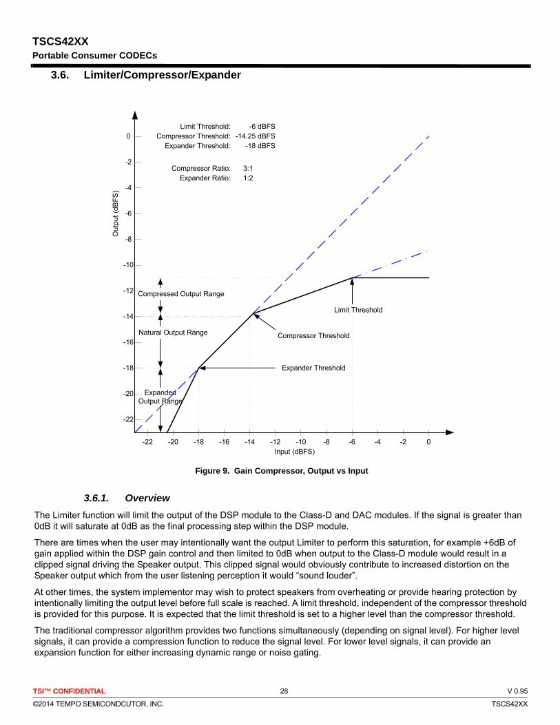
TSI™ CONFIDENTIAL 28 V 0.95
©2014 TEMPO SEMICONDCUTOR, INC. TSCS42XX
TSCS42XXPortable Consumer CODECs
3.6. Limiter/Compressor/Expander
Figure 9. Gain Compressor, Output vs Input
3.6.1. Overview
The Limiter function will limit the output of the DSP module to the Class-D and DAC modules. If the signal is greater than 0dB it will saturate at 0dB as the final processing step within the DSP module.
There are times when the user may intentionally want the output Limiter to perform this saturation, for example +6dB of gain applied within the DSP gain control and then limited to 0dB when output to the Class-D module would result in a clipped signal driving the Speaker output. This clipped signal would obviously contribute to increased distortion on the Speaker output which from the user listening perception it would “sound louder”.
At other times, the system implementor may wish to protect speakers from overheating or provide hearing protection by intentionally limiting the output level before full scale is reached. A limit threshold, independent of the compressor threshold is provided for this purpose. It is expected that the limit threshold is set to a higher level than the compressor threshold.
The traditional compressor algorithm provides two functions simultaneously (depending on signal level). For higher level signals, it can provide a compression function to reduce the signal level. For lower level signals, it can provide an expansion function for either increasing dynamic range or noise gating.
Out
put (
dBF
S)
Input (dBFS)0-2-4-6-8-10-12-14-16-18-20-22
-16
-18
-20
-22
-14
-12
-10
-8
-6
-4
-2
0Limit Threshold:
Compressor Threshold:
Compressor Ratio: 3:1
-14.25 dBFS-6 dBFS
Expander Threshold: -18 dBFS
Expander Ratio: 1:2
ExpandedOutput Range
Natural Output Range
Compressed Output Range
Compressor Threshold
Expander Threshold
Limit Threshold

TSI™ CONFIDENTIAL 29 V 0.95
©2014 TEMPO SEMICONDCUTOR, INC. TSCS42XX
TSCS42XXPortable Consumer CODECs
The compressor monitors the signal level and, if the signal is higher than a threshold, will reduce the gain by a programmed ratio to restrict the dynamic range. Limiting is an extreme example of the compressor where, as the input signal level is increased, the gain is decreased to maintain a specific output level.
In addition to limiting the bandwidth of the compressed audio, it is common for compressed audio to also compress the dynamic range of the audio. The expansion function inTSCS42XX can help restore the original dynamics to the audio.
The expander is a close relative of the compressor. Rather than using signal dependent gain to restrict the dynamic range, the expander uses signal dependent gain to expand the dynamic range. Thus if a signal level is below a particular threshold, the expander will reduce the gain even further to extend the dynamic range of the material.
3.6.2. Configuration
This compressor limiter provides the following configurable parameters.
• Compressor/limiter• Threshold – The threshold above which the compressor will reduce the dynamic range of
the audio in the compression region.• Ratio – The ratio between the input dynamic range and the output dynamic range. For
example, a ratio of 3 will reduce an input dynamic range of 9db to 3db. • Attack Time – The amount of time that changes in gain are smoothed over during the attack
phase of the compressor. • Release Time – The amount of time that changes in gain are smoothed over during the
release phase of the compressor. • Makeup gain – Used to increase the overall level of the compressed audio.
• Expander • Threshold – The threshold below which the expander will increase the dynamic range of the
audio. • Ratio – The ratio between the input dynamic range and the output dynamic range of the
audio in the expansion range. For example a ratio of 3 will take an input dynamic range of 9db and expand it to 27db.
• Attack Time – The amount of time that changes in gain are smoothed over during the attack phase of the expander
• Release Time• - The amount of time that changes in gain are smoothed over during the release phase of
the expander.
• Two level detection algorithms• RMS – Use an RMS measurement for the level. • Peak – Use a peak measurement for the level.

TSI™ CONFIDENTIAL 30 V 0.95
©2014 TEMPO SEMICONDCUTOR, INC. TSCS42XX
TSCS42XXPortable Consumer CODECs
3.6.3. Controlling parameters
IIn order to control this processing, there are a number of configurable parameters. The parametersand their ranges are:
• Compressor/limiter• Threshold – -40db to 0db relative to full scale.• Ratio – 1 to 20• Attack Time – typically 0 to 500ms• Release Time – typically 25ms to 2 seconds• Makeup gain – 0 to 40db
• Expander• Threshold – -30 to -60 dB• Ratio – 1 to 6• Attack Time – same as above• Release Time – same as above.
• Two level detection algorithms• RMS• Peak
3.6.4. Limiter/Compressor/Expander Registers
3.6.4.1. General compressor/limiter/expander control Register
Table 43. CLECTL Register
Register Address Bit Label Type Default Description
R37 (25h)CLECTL
7:5 RSVD R 0h Reserved
4 Lvl_Mode RW 0 CLE Level Detection Mode0 = Average1 = Peak
3 WindowSel RW 0 Window width selection for level detection:
0 = equivalent of 512 samples of selected Base Rate (~10-16ms)1 = equivalent of 64 samples of selected Base Rate (~1.3-2ms)
2 Exp_en RW 0 1 = enable expander
1 Limit_en RW 0 1 = enable limiter
0 Comp_en RW 0 1 = enable compressor

TSI™ CONFIDENTIAL 31 V 0.95
©2014 TEMPO SEMICONDCUTOR, INC. TSCS42XX
TSCS42XXPortable Consumer CODECs
3.6.4.2. Compressor/Limiter/Expander make-up gain Register
Table 44. MUGAIN Register
3.6.4.3. Compressor Threshold Register
Table 45. COMPTH Register
3.6.4.4. Compressor ration register
Table 46. CMPRAT Register
3.6.4.5. Compressor Attack Time Constant Register (Low)
Table 47. CATKTCL Register
Register Address Bit Label Type Default Description
R38 (26h)MUGAIN
7:5 RSVD R 0h Reserved
4:0 CLEMUG[4:0] RW 0h 0dB...46.5dB in 1.5dB steps
Register Address Bit Label Type Default Description
R39 (27h)COMPTH
7:0 COMPTH[7:0] RW 00h FFh...00h = 0dB...95.625dB in 0.375dB steps.
Register Address Bit Label Type Default Description
R40 (28h)CMPRAT
7:5 RSVD R 000 Reserved
4:0 CMPRAT[4:0] RW 00h Compressor Ratio00h = Reserved01h = 1.5:102h...14h = 2:1...20:115h...1Fh = Reserved
Register Address Bit Label Type Default Description
R41 (29h)CATKTCL
7:0 CATKTC[7:0] RW 00h Low byte of the time constant used to ramp to a new gain value during a compressor attack phase.

TSI™ CONFIDENTIAL 32 V 0.95
©2014 TEMPO SEMICONDCUTOR, INC. TSCS42XX
TSCS42XXPortable Consumer CODECs
3.6.4.6. Compressor Attack Time Constant Register (High)
Table 48. CATKTCH Register
3.6.4.7. Compressor Release Time Constant Register (Low)
Table 49. CRELTCL Register
3.6.4.8. Compressor Release Time Constant Register (High)
Table 50. CRELTCH Register
3.6.4.9. Limiter Threshold Register
Table 51. LIMTH Register
Register Address Bit Label Type Default Description
R42 (2Ah)CATKTCH
7:0 CATKTC[15:8] RW 00h High byte of the time constant used to ramp to a new gain value during a compressor attack phase. The time constant is [high byte, low byte]0000h = 0 (instantaneous)0001h = 0.96875 + 1/(2^21)0002h = 0.96875 + 2/(2^21)... (step = 1/(2^21))FFFEh = [(2^21)-2]/(2^21)FFFFh = [(2^21)-1]/(2^21)
Register Address Bit Label Type Default Description
R43 (2Bh)CRELTCL
7:0 CRELTC[7:0] RW 00h Low byte of the time constant used to ramp to a new gain value during a compressor release phase.
Register Address Bit Label Type Default Description
R44 (2Ch)CRELTCH
7:0 CRELTC[15:8] RW 00h High byte of the time constant used to ramp to a new gain value during a compressor release phase. The time constant is [high byte, low byte]0000h = 0 (instantaneous)0001h = 0.96875 + 1/(2^21)0002h = 0.96875 + 2/(2^21)... (step = 1/(2^21))FFFEh = [(2^21)-2]/(2^21)FFFFh = [(2^21)-1]/(2^21)
Register Address Bit Label Type Default Description
R45 (2Dh)LIMTH
7:0 LIMTH[7:0] RW 00h FFh...00h = 0dB...95.625dB in 0.375dB steps.

TSI™ CONFIDENTIAL 33 V 0.95
©2014 TEMPO SEMICONDCUTOR, INC. TSCS42XX
TSCS42XXPortable Consumer CODECs
3.6.4.10. Limiter Target Register
Table 52. LIMTGT Register
3.6.4.11. Limiter Attack Time Constant Register (Low)
Table 53. LATKTCL Register
3.6.4.12. Limiter Attack Time Constant Register (High)
Table 54. LATKTCH Register
3.6.4.13. Limiter Release Time Constant Register (Low)
Table 55. LRELTCL Register
Register Address Bit Label Type Default Description
R46 (2Eh)LIMTGT
7:0 LIMTGT[7:0] RW 00h FFh...00h = 0dB...95.625dB in 0.375dB steps.
Register Address Bit Label Type Default Description
R47 (2Fh)LATKTCL
7:0 LATKTC[7:0] RW 00h Low byte of the time constant used to ramp to a new gain value during a limiter attack phase.
Register Address Bit Label Type Default Description
R48 (30h)LATKTCH
7:0 LATKTC[15:8] RW 00h High byte of the time constant used to ramp to a new gain value during a limiter attack phase. The time constant is [high byte, low byte]0000h = 0 (instantaneous)0001h = 0.96875 + 1/(2^21)0002h = 0.96875 + 2/(2^21)... (step = 1/(2^21))FFFEh = [(2^21)-2]/(2^21)FFFFh = [(2^21)-1]/(2^21)
Register Address Bit Label Type Default Description
R49 (31h)LRELTCL
7:0 LRELTC[7:0] RW 00h Low byte of the time constant used to ramp to a new gain value during a limiter release phase.

TSI™ CONFIDENTIAL 34 V 0.95
©2014 TEMPO SEMICONDCUTOR, INC. TSCS42XX
TSCS42XXPortable Consumer CODECs
3.6.4.14. Limiter Release Time Constant Register (High)
Table 56. LRELTCH Register
3.6.4.15. Expander Threshold Register
Table 57. EXPTH Register
3.6.4.16. Expander Ratio Register
Table 58. EXPRAT Register
3.6.4.17. Expander Attack Time Constant Register (Low)
Table 59. XATKTCL Register
Register Address Bit Label Type Default Description
R50 (32h)LRELTCH
7:0 LRELTC[15:8] RW 00h High byte of the time constant used to ramp to a new gain value during a limiter release phase. The time constant is [high byte, low byte]0000h = 0 (instantaneous)0001h = 0.96875 + 1/(2^21)0002h = 0.96875 + 2/(2^21)... (step = 1/(2^21))FFFEh = [(2^21)-2]/(2^21)FFFFh = [(2^21)-1]/(2^21)
Register Address Bit Label Type Default Description
R51 (33h)EXPTH
7:0 EXPTH[7:0] RW 00h Expander threshold: 0...95.625dB in 0.375dB steps
Register Address Bit Label Type Default Description
R52 (34h)EXPRAT
7:3 RSVD R 00h Reserved
2:0 EXPRAT[2:0] RW 000 Expander Ratio 0h...1h = Reserved2h...7h = 1:2...1:7
Register Address Bit Label Type Default Description
R53 (35h)XATKTCL
7:0 XATKTC[7:0] RW 00h Low byte of the time constant used to ramp to a new gain value during a expander attack phase.
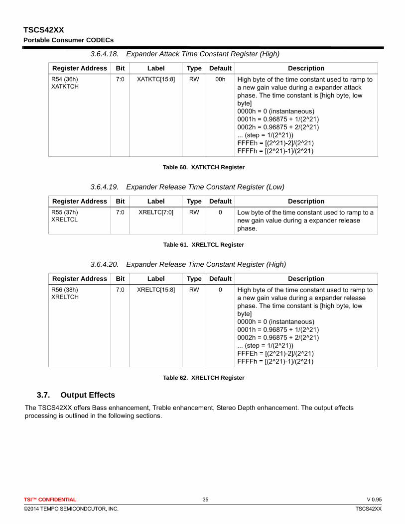
TSI™ CONFIDENTIAL 35 V 0.95
©2014 TEMPO SEMICONDCUTOR, INC. TSCS42XX
TSCS42XXPortable Consumer CODECs
3.6.4.18. Expander Attack Time Constant Register (High)
Table 60. XATKTCH Register
3.6.4.19. Expander Release Time Constant Register (Low)
Table 61. XRELTCL Register
3.6.4.20. Expander Release Time Constant Register (High)
Table 62. XRELTCH Register
3.7. Output Effects
The TSCS42XX offers Bass enhancement, Treble enhancement, Stereo Depth enhancement. The output effects processing is outlined in the following sections.
Register Address Bit Label Type Default Description
R54 (36h)XATKTCH
7:0 XATKTC[15:8] RW 00h High byte of the time constant used to ramp to a new gain value during a expander attack phase. The time constant is [high byte, low byte]0000h = 0 (instantaneous)0001h = 0.96875 + 1/(2^21)0002h = 0.96875 + 2/(2^21)... (step = 1/(2^21))FFFEh = [(2^21)-2]/(2^21)FFFFh = [(2^21)-1]/(2^21)
Register Address Bit Label Type Default Description
R55 (37h)XRELTCL
7:0 XRELTC[7:0] RW 0 Low byte of the time constant used to ramp to a new gain value during a expander release phase.
Register Address Bit Label Type Default Description
R56 (38h)XRELTCH
7:0 XRELTC[15:8] RW 0 High byte of the time constant used to ramp to a new gain value during a expander release phase. The time constant is [high byte, low byte]0000h = 0 (instantaneous)0001h = 0.96875 + 1/(2^21)0002h = 0.96875 + 2/(2^21)... (step = 1/(2^21))FFFEh = [(2^21)-2]/(2^21)FFFFh = [(2^21)-1]/(2^21)

TSI™ CONFIDENTIAL 36 V 0.95
©2014 TEMPO SEMICONDCUTOR, INC. TSCS42XX
TSCS42XXPortable Consumer CODECs
3.7.1. FX Control Register
Table 63. FXCTL Register
3.7.2. Stereo Depth (3-D) Enhancement
The TSCS42XX has a digital depth enhancement option to artificially increase the separation between the left and right channels, by enabling the attenuation of the content common to both channels. The amount of attenuation is programmable within a range. The input is prescaled (fixed) before summation to prevent saturation.
The 3-D enhancement algorithm is a tried and true algorithm that uses two principles.
1 If the material common to the two channels is removed, then the output will sound more 3-D.
2 If the material for the opposite channel is presented to the current channel inverted, it will tend to cancel any material from the opposite channel on the current ear. For example, if the material from the right is presented to the left ear inverted, it will cancel some of the material from the right ear that is leaking into the right ear.
Figure 10. 3-D Channel Inversion
Note: .3D_Mix specifies the amount of the common signal that is added from the left and right channels. This number is a fractional amount between -1 and 1. For proper operation, this value is typically negative.
Register Address Bit Label Type Default Description
R57 (39h)FXCTL
7:5 RSVD R 000 Reserved
4 3DEN RW 0 3D Enhancement Enable0 = Disabled1 = Enabled
3 TEEN RW 0 Treble Enhancement Enable0 = Disabled1 = Enabled
2 TNLFBYP RW 0 Treble Non-linear Function Bypass:0 = Enabled1 = Bypassed
1 BEEN RW 0 Bass Enhancement Enable0 = Disabled1 = Enabled
0 BNLFBYP RW 0 Bass Non-linear Function Bypass:0 = Enabled1 = Bypassed
Left Left
Right Right

TSI™ CONFIDENTIAL 37 V 0.95
©2014 TEMPO SEMICONDCUTOR, INC. TSCS42XX
TSCS42XXPortable Consumer CODECs
3.7.3. Psychoacoustic Bass Enhancement
One of the primary audio quality issues with small speaker systems is their inability to reproduce significant amounts of energy in the bass region (below 200Hz). While there is no magic mechanism to make a speaker reproduce frequencies that it is not capable of, there are mechanisms for fooling the ear into thinking that the bass material is being heard.
The psychoacoustic bass processor relies on a psychoacoustic principle called “missing fundamental”. If the human ear hears a proper series of harmonics for a particular bass note, the listener will hear the fundamental of that series, even if it is not present.
A processing algorithm using this principle allows for improving the apparent low frequency response of an audio system below what it is actually capable of. Below is a diagram of the implementation of this algorithm.
Figure 11. Bass Enhancement
3.7.4. Treble Enhancement
One of the mechanisms used to limit the bit rate for compressed audio is to first remove high frequency information before compression. When these files are decompressed, this can lead to dull sounding audio. The TSI treble enhancement replaces these lost high frequencies.
The enhanced treble function works much like the enhanced bass, however it's intended use is different. The Enhanced treble uses a non linear function to add treble harmonics to a signal that has limited high-frequency bandwidth (such as a low bit rate MP3). In this case, the algorithm makes use of the audio fact that presence of audio between 4-8K is a good predictor of audio between 10K-20K.
Figure 12. Treble Enhancement
The enhanced treble NLF has a different set of requirements than the psychoacoustic bass. In particular, the presence of odd high frequency harmonics is objectionable. Thus the most promising NLF for enhanced treble is a half wave rectifier.
NLF
Extract Filter
LimitFilter
Cutoff Filter
NLF
Extract Filter
LimitFilter

TSI™ CONFIDENTIAL 38 V 0.95
©2014 TEMPO SEMICONDCUTOR, INC. TSCS42XX
TSCS42XXPortable Consumer CODECs
3.8. Mute and De-Emphasis
The TSCS42XX has a Soft Mute function, which is used to gradually attenuate the digital signal volume to zero. The gain returns to its previous setting if the soft mute is removed. At startup, the codec is muted by default; to enable audio play, the mute bit must be cleared to 0.
After the equalization filters, de-emphasis may be performed on the audio data to compensate for pre-emphasis that may be included in the audio stream. De-emphasis filtering is only available for 48kHz, 44.1kHz, and 32kHz sample rates.
3.9. Mono Operation and Phase Inversion
Normal stereo operation converts left and right channel digital audio data to analog in separate DACs. However, it is also possible to have the same signal (left or right) appear on both analog output channels by disabling one channel; alternately, there is a mono-mix mode that mixes the two channels digitally before converting to analog using only one DAC. In this mode, the other DAC is switched off, and the resulting mixed stream signal can appear on both analog output channels.
The DAC output defaults to non-inverted. Setting DACPOLL and DACPOLR bits will invert the DAC output phase on the left and right channels.
3.9.1. DAC Control Register
3.10. Analog Outputs
3.10.1. Headphone Output
The HPOut pins can drive a 16Ohm or 32Ohm headphone or alternately drive a line output. The signal volume of theheadphone amplifier can be independently adjusted under software control by writing to HPVOL_L and HPVOL_R.Setting the volume to 0000000 will mute the output driver; the output remains at ground, so that no click noise is pro-duced when muting or un-muting. Gains above 0dB run the risk of clipping large signals.To minimize artifacts such as clicks and zipper noise, the headphone and BTL outputs feature a volume fade functionthat smoothly changes volume from the current value to the target value.
Register Address Bit Label Type Default Description
R24 (18h)CNVRTR1
7 DACPOLR RW 0 Invert DAC Right signal
6 DACPOLL RW 0 Invert DAC Left signal
5:4DMONOMIX
[1:0]RW 00
DAC mono mix00: stereo01: mono ((L/2)+(R/2)) into DACL, ‘0’ into DACR10: mono ((L/2)+(R/2)) into DACR, ‘0’ into DACL11: mono ((L/2)+(R/2)) into DACL and DACR
3 DACMU RW 1Digital Soft Mute1 = mute0 = no mute (signal active)
2 DEEMP RW 0De-emphasis Enable1 = Enabled0 = Disable
1:0 DACDITH RW 00
DAC Dither Mode:0 = Dynamic, half amplitude1 = Dynamic, full amplitude2 = DAC dither disabled3 = Static
Table 64. CNVRTR1 Register
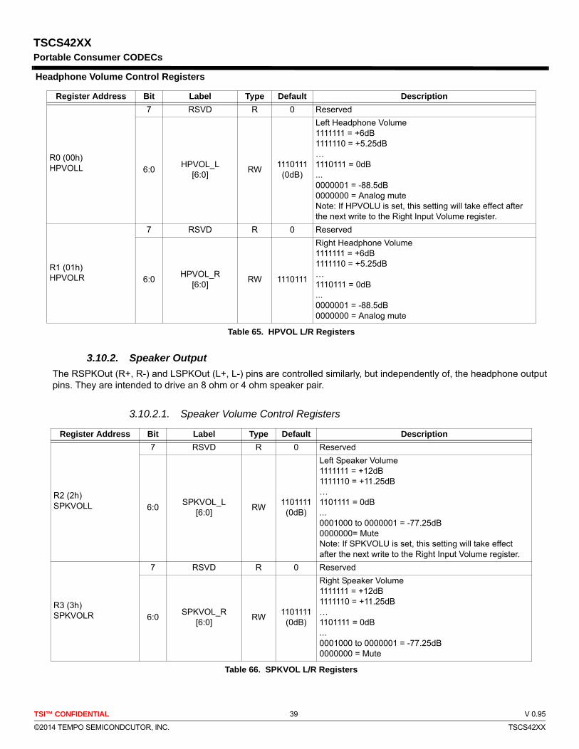
TSI™ CONFIDENTIAL 39 V 0.95
©2014 TEMPO SEMICONDCUTOR, INC. TSCS42XX
TSCS42XXPortable Consumer CODECs
Headphone Volume Control Registers
3.10.2. Speaker Output
The RSPKOut (R+, R-) and LSPKOut (L+, L-) pins are controlled similarly, but independently of, the headphone outputpins. They are intended to drive an 8 ohm or 4 ohm speaker pair.
3.10.2.1. Speaker Volume Control Registers
Register Address Bit Label Type Default Description
R0 (00h)HPVOLL
7 RSVD R 0 Reserved
6:0HPVOL_L
[6:0]RW
1110111(0dB)
Left Headphone Volume1111111 = +6dB1111110 = +5.25dB…1110111 = 0dB...0000001 = -88.5dB0000000 = Analog muteNote: If HPVOLU is set, this setting will take effect after the next write to the Right Input Volume register.
R1 (01h)HPVOLR
7 RSVD R 0 Reserved
6:0HPVOL_R
[6:0]RW 1110111
Right Headphone Volume1111111 = +6dB1111110 = +5.25dB…1110111 = 0dB...0000001 = -88.5dB0000000 = Analog mute
Table 65. HPVOL L/R Registers
Register Address Bit Label Type Default Description
R2 (2h)SPKVOLL
7 RSVD R 0 Reserved
6:0SPKVOL_L
[6:0]RW
1101111(0dB)
Left Speaker Volume1111111 = +12dB1111110 = +11.25dB…1101111 = 0dB...0001000 to 0000001 = -77.25dB0000000= MuteNote: If SPKVOLU is set, this setting will take effect after the next write to the Right Input Volume register.
R3 (3h)SPKVOLR
7 RSVD R 0 Reserved
6:0SPKVOL_R
[6:0]RW
1101111(0dB)
Right Speaker Volume1111111 = +12dB1111110 = +11.25dB…1101111 = 0dB...0001000 to 0000001 = -77.25dB0000000 = Mute
Table 66. SPKVOL L/R Registers
TSI™ CONFIDENTIAL 40 V 0.95
©2014 TEMPO SEMICONDCUTOR, INC. TSCS42XX
TSCS42XXPortable Consumer CODECs
3.10.3. DDXTMClass D Audio Processing
For additional information on the DDXTM Class D solution, please see the application note onwww.Temposemi.com.
The DDXTM Class D PWM Controller performs the following signal processing:
• Feedback filters are applied to shape any noise. The filters move noise from audible frequencies to frequencies above the audio range.
• The PWM block converts the data streams to tri-state PWM signals and sends them to the power stages.
• Finally, the Class-D controller block adjusts the output volume to provide constant output power across supply voltage.
The power stages boost the signals to higher levels, sufficient to drive speakers at a comfortable lis-tening level.
3.10.3.1. Constant Output Power Mode
In normal operation the BTL amplifier is rated at 0.5W (full scale digital with 6dB BTL gain) into an 8ohm load at 3.6V but will vary from about 0.38W to about 1.2W across a 3.1V to 5.5V supply range.However, when constant output power mode is enabled, the full scale output is held constant from3.1V to 5.5V.
The BTL amplifier in TSCS42XX will continuously adjust to power supply changes to ensure that thefull scale output power remains constant. This is not an automatic level control. Rather, this functionprevents sudden volume changes when switching between battery and line power. Please note,when in this mode the amplifier efficiency may be reduced and decreases with higher supply volt-ages and lower target values.
A simple 5-bit ADC is used to monitor PVDD. As PVDD raises or lowers, the analog circuit will senda 5-bit code to the digital section that will average and then calculate a gain adjustment. The BTLaudio signal will be multiplied by this gain value (in addition to the user volume controls).
The user will select a target value for the circuit. The constant output function will calculate a gainadjustment that will provide approximately the same full scale output voltage as provided whenPVDD causes the same code value. So, if the target is 9 then a PVDD voltage of about 3.7V wouldgenerate a code value of 9 and a full scale output power of about 630mW into 8 ohms. If PVDDshould rise to 4V, generating a code of 13, then the constant output power circuit would reduce thegain by 0.75dB (4 codes * 0.1875dB) to keep the full scale output at the target level.
The circuit may be configured to add gain, attenuation, or both to maintain the full-scale output level.If the needed adjustment falls outside of the range of the circuit (only attenuation is enabled and gainis needed, for example) then the circuit will apply as much correction as it is able. Through the use of

TSI™ CONFIDENTIAL 41 V 0.95
©2014 TEMPO SEMICONDCUTOR, INC. TSCS42XX
TSCS42XXPortable Consumer CODECs
gain, attenuation, and target values, different behaviors may be implemented:
• Attenuation only, target set to mimic a low supply voltage - Constant output level across bat-tery state with constant quality (THD/SNR)
• Attenuation only, target set to mimic a moderate supply voltage - Output limiting to an approximate power level. Level will decrease at lower supply voltages but won’t increase beyond a specific point.
• Gain only, target at or near max - Output will remain relatively constant but distortion will increase as PVDD is lowered. This mimics the behavior of common class-AB amplifiers.
• Gain and attenuation - Output remains at a level below the maximum possible at the highest supply voltage and above the theoretical full scale at minimum supply. Full scale PCM input clips when the supply voltage is low but won’t become too loud when the supply voltage is high.
In addition to maintaining a constant output level, PVDD may be monitored for a large, sudden,change. If the High Delta function is enabled and PVDD changes more than 4 code steps since thelast cycle, the output will be rapidly reduced then gradually increased to the target level.
When using this circuit, please take note of the following:
• The full scale output power may be limited by the supply voltage.• Full scale output power is affected by other gain controls in the output path including the EQ
and compressor/limiter.• The Constant Output Power function is intended to help maintain a constant output level, not
an exact output level. The output level for a specific target may vary part to part. If limiting is required for safety or other reasons, be conservative and set the target well below the maxi-mum allowable level.
• Noise on the PVDD supply may cause erratic behavior. Use the recommended supply decoupling caps and verify that the power supply can support the peak currents demanded by a class-D amplifier.

TSI™ CONFIDENTIAL 42 V 0.95
©2014 TEMPO SEMICONDCUTOR, INC. TSCS42XX
TSCS42XXPortable Consumer CODECs
Constant Output Power error (dB) relative to a target of 8 for an ideal part and the output error if leftuncorrected across a 3.1 to 5.5V supply range.
Figure 13. Constant Output Power Error
Constant Output Power for nominal and high/low reference across a 3.1 to 5.5V supplyrange.(Uncorrected power shown for reference) A target of 8 roughly corresponds to 0.5W at 3.6Vinto 8 ohms.
Figure 14. Constant Output Power nominal and high/low
‐3
‐2
‐1
0
1
2
3
3.1 4.1 5.1
relative to target
Nom dB
0.2
0.3
0.4
0.5
0.6
0.7
0.8
0.9
1
1.1
1.2
3.1 4.1 5.1
Off
Nom
Hi
Low

TSI™ CONFIDENTIAL 43 V 0.95
©2014 TEMPO SEMICONDCUTOR, INC. TSCS42XX
TSCS42XXPortable Consumer CODECs
3.10.3.2. Under Voltage Lock Out
When the PVDD supply becomes low, the BTL amplifier may be disabled to help prevent undesir-able amplifier operation (overheat) or system level problems (battery under-voltage.)
The same circuit that monitors the PVDD supply to help maintain a constant output power is used tomonitor the PVDD supply for a critical under-voltage situation. If the sense circuit consistently returnsa 0 code then the PVDD supply is less than the minimum required for proper operation. To preventaccidental shutdown due to a noisy supply at the minimum operating range, the output of the PVDDsense circuit will be averaged for at least 200ms.
3.10.3.3. Register
Registers Constant Output Power 1
Registers Constant Output Power 2
Register Address Bit Label Type Default Description
R34 (22h)COP1
7 COPAtten RW 01 = Constant Output Power function will use attenuate the BTL output if the PVDD sense circuit returns a code higher than the target value.
6 COPGain RW 01 = Constant Output Power function will use attenuate the BTL output if the PVDD sense circuit returns a code higher than the target value.
5 HDeltaEn RW 01 = If the PVDD code value has changed more than 4 counts since the last gain adjustment, the output will be reduced rapidly then slowly returned to the target level.
4:0 COPTarget[4:0] RW 8h 5-bit target for the Constant Output Power function.
Table 67. COP1 Register
Register Address Bit Label Type Default Description
R35 (23h)COP2
7 RSVD R 0 Reserved
6 RSVD R 0 Reserved
5:3 AvgLength[2:0] RW 000
Constant Output Power Average Length (number of supply detect cycles to average):0h = 11h = 22h = 43h = 84h = 165h = 326h = 647h = 1288h = 2569h = 512Ah-Fh = Reserved
2:0 MonRate[2:0] RW 100
Supply Detect Monitor Rate:0h = 0.25ms1h = 0.5ms2h = 1ms3h = 2ms
Table 68. COP2 Register

TSI™ CONFIDENTIAL 44 V 0.95
©2014 TEMPO SEMICONDCUTOR, INC. TSCS42XX
TSCS42XXPortable Consumer CODECs
Registers Constant Output Power 3
Configuration Register
Register Address Bit Label Type Default Description
R137 (89h)COP3
7 HIGHDELTA R 0
Constant Output Power High Delta Status:0 = No high delta event is currently being detected or recovered from1 = A high delta event has been detected and the COP function is adjusting.
6 UNDERVOLTAGE R 0Under Voltage Lockout Status:0 = Supply is not below the UVLO threshold1 = Supply is below the UVLO threshold.
5:0 COPADJ R 0h
Constant Output Power Adjustment Status (0.1875dB Steps, Twos Complement Value):20h = -6dB21h = -5.8125dB... FFh = -0.1875dB00h = 0dB01h = +0.1875dB... 1Fh = +5.8125dB
Table 69. COP3 Register
Register Address Bit Label Type Default Description
R31 (1Fh)CONFIG0
7:6 ASDM[1:0] RW 10h
ADC Modulater Rate:00b = Reserved01b = Half10b = Full11b = Auto
5:4 DSDM[1:0] RW 10h
DAC Modulater Rate:00b = Reserved01b = Half10b = Full11b = Auto
3:2 RSVD R 0h Reserved for future use.
1 DC_BYPASS RW 0DAC DC Filter Bypass:0 = Filter enabled1 = Filter bypassed
0 SD_FORCE_ON RW 0
Supply Detect Force On:0 = Supply detect not forced on1 = Supply detect forced on.
Note:If not forced on, the supply detect logic will automatically be enabled when features that use it are enabled (COP, UVLO
Table 70. CONFIG0 Register

TSI™ CONFIDENTIAL 45 V 0.95
©2014 TEMPO SEMICONDCUTOR, INC. TSCS42XX
TSCS42XXPortable Consumer CODECs
PWM Control 0 Register
PWM Control 1 Register
PWM Control 2 Register
Register Address Bit Label Type Default Description
R66 (42h)PWM0
7:6 SCTO RW 11
Class-D Short Circuit Detect Time-out00 = 10uS01 = 100uS10 = 500uS11 = 100mS
5 UVLO RW 1Under Voltage Lock Out1 = BTL output disabled if PVDD sense circuit returns code 0
4 RESERVED RW 1 Reserved
3 BFCLR RW 0PWM Noise Shaper Clear:0 = Filter enabled1 = Filter disabled.
2 PWMMODEr RW 1PWM Modulation Type:0 = Binary1 = Ternary
1 RESERVED RW 0 Reserved
0 NOOFFSET RW 0No Offset between left/right PWM frames:0 = Frames offset1 = Frames aligned
Table 71. PWM0 Register
Register Address Bit Label Type Default Description
R67 (43h)PWM1
7 RSVD R 0 Reserved
6:2 dithpos[4:0] RW 0
Dither position, where dither inserted after NS.0,1,2 = dither bits 2:04 = dither bits 3:15 = dither bits 4:1....19 = dither bits 19:17
1 dith_range RW 0 1 = dither -1 to +1, 0 = -3 to +3
0 dithclr RW 0 1 = disable dither
Table 72. PWM1 Register
Register Address Bit Label Type Default Description
R68 (44h)PWM2
7:2 R 0h Reserved
1 R 0 Reserved
0 R 0 Reserved
Table 73. PWM2 Register

TSI™ CONFIDENTIAL 46 V 0.95
©2014 TEMPO SEMICONDCUTOR, INC. TSCS42XX
TSCS42XXPortable Consumer CODECs
PWM Control 3 Register
3.10.4. Other Output Capabilities
Each audio analog output can be separately enabled. Disabling outputs serves to reduce power consumption, and isthe default state of the device.
3.10.4.1. Audio Output Control
See Power management section. The output enable bits are also power management bits and theoutputs will be turned off when disabled.
3.10.5. Headphone Switch
The HP_DET pin is used to detect connection of a headphone. When headphone insertion isdetected, the codec can automatically disable the speaker outputs and enable the headphone out-puts. Control bits determine the meaning and polarity of the input.
Register Address Bit Label Type Default Description
R69 (45h)PWM3
7:6 outctrl[1:0] RW 0h
pwm output muxing0 = normal1 = swap 0/12 = ch0 on both3 = ch1 on both
5:3 R 0h Reserved
2:0 cvalue[2:0] RW 3h PWM C Value
Table 74. PWM3 Register
Register Address Bit Label Type Default Description
R27 (1Bh)PWRM2
7 D2S RW 0Analog Input D2S:0 = Power down1 = Power up
6 HPL RW 0Headphone Left Output Buffer + DAC:0 = Power down1 = Power up
5 HPR RW 0Headphone Right Output Buffer + DAC:0 = Power down1 = Power up
4 SPKL RW 0Speaker Left Output Buffer:0 = Power down1 = Power up
3 SPKR RW 0Speaker Right Output Buffer:0 = Power down1 = Power up
2 RSVD RW 0 Reserved(bit implemented but unused)1 RSVD RW 0 Reserved (bit implemented bur unused)
0 VREF RW 1Vref (necessary for all other functions):0 = Power down1 = Power up
Note: A value of “1” indicates the output is enabled; a value of ‘0’ disables the output.
Table 75. PWRM2 Register

TSI™ CONFIDENTIAL 47 V 0.95
©2014 TEMPO SEMICONDCUTOR, INC. TSCS42XX
TSCS42XXPortable Consumer CODECs
In addition to enabling and disabling outputs, the EQ may also be controlled using the HP_DET pin.The 2 EQ filters may be configured so that one EQ is active when the Headphone output is activeand the other EQ is active when the Speaker output is active (independent HP and Speaker EQ).One EQ may be enabled only when the Speaker is active and the other EQ may be on when eitherof the outputs are active (Speaker compensation and USER EQ) or other combinations are possible.Note that the EQ coefficients must be programmed and the EQs must be enabled using their controlregisters. The HP_DET logic can only disable the EQ filters.
3.10.5.1. Headphone Switch Register
Register Address Bit Label Type Default Description
R28 (1Ch)CTL
7 HPSWEN RW 0hHeadphone Switch Enable:0 = Headphone switch disabled1 = Headphone switch enabled
6 HPSWPOL RW 0hHeadphone Switch Polarity:0 = HPDETECT high indicates headphone1 = HPDETECT high indicates speaker
5:4 EQ2SW RW 0h
EQ2 behavior due to speaker/headphone output state:00b = EQ is not disabled due to headphone/speaker logic01b = EQ is disabled when headphone output is active10b = EQ is disabled when speaker output is active11b = EQ is disabled when headphone AND speaker output are active
3:2 EQ1SW RW 0h
EQ1 behavior due to speaker/headphone output state:00b = EQ is not disabled due to headphone/speaker logic01b = EQ is disabled when headphone output is active10b = EQ is disabled when speaker output is active11b = EQ is disabled when headphone AND speaker output are active
1 TSDEN RW 0hThermal Shutdown Enable (See section 7.9)0: thermal shutdown disabled1: thermal shutdown enabled
0 TOEN RW 0h
Zero Cross Time-out Enable0: Time-out Disabled1: Time-out Enabled - volumes updated if no zero cross event has occurred before time-out
Table 76. CTL Register

TSI™ CONFIDENTIAL 48 V 0.95
©2014 TEMPO SEMICONDCUTOR, INC. TSCS42XX
TSCS42XXPortable Consumer CODECs
3.10.5.2. Speaker Operation
3.10.5.3. EQ Operation
HPSWEN HPSWPOLHP_DET Pin state SPKOut1
1.SPKOut = Logical OR of the SPKL and SPKR enable(power state) bits
Speaker Enabled
0 X X 0 no
0 X X 1 yes
1 0 0 0 no
1 0 0 1 yes
1 0 1 X no
1 1 0 X no
1 1 1 0 no
1 1 1 1 yes
Table 77. Speaker Operation
EQnSW1 EQnSW0 EQ Behavior1
1.EQ must be enabled. EQ behavior is dependent on HP_DET and Output powerstate programming.
0 0 EQ is not disabled due to Headphone/Speaker logic
0 1 EQ is disabled when Headphone output is active
1 0 EQ is disabled when Speaker output is active
1 1 EQ is disabled when Headphone AND Speaker output are active
Table 78. EQ Operation
TSI™ CONFIDENTIAL 49 V 0.95
©2014 TEMPO SEMICONDCUTOR, INC. TSCS42XX
TSCS42XXPortable Consumer CODECs
3.11. Thermal Shutdown
To avoid overpowering and overheating the codec when the amplifier outputs are driving large currents, the TSCS42XXincorporates a thermal protection circuit. If enabled, and the device temperature reaches approximately 150°C, thespeaker and headphone amplifier outputs will be disabled. Once the device cools, the outputs will be automaticallyre-enabled.
3.11.1. Algorithm description:
There are 2 trip points, “high” and “low”. High indicates a critical overheat requiring a reduction in vol-ume to avoid damage to the part. Low is set for a slightly lower temperature point, indicating that thecurrent level is safe but that increased volume would result in a critical overheat condition.
Normally, the overheat bits are polled every 8ms but may be polled at 4ms, 8ms, 16ms, or 32ms byadjusting the Poll value. Reductions in volume will be allowed to happen at the Poll rate. Increases involume are programmable to happen every 1, 2, 4, or 8 Poll cycles and in steps of 0.75dB to 6dB.This allows a full scale volume increase in a range of 10s of milliseconds to 10s of seconds.
When both overheat bits are 0, the volume is allowed to increment by the IncStep size, unless thevolume has already reached the maximum value allowed. Any subsequent increment will be held offuntil the programmed number of polling cycles have occurred.
When the low overheat bit is 1 and the high overheat bit is 0, this indicates that the volume is cur-rently at a safe point but the temperature is higher than desired and incrementing the volume maycause severe overheating. The volume is held at the current value.
When the high overheat bit is 1, damage could occur, so the volume setting will be immediatelyreduced by the Decrement Step value. As the overheat bits are re-polled, this volume reduction willcontinue until the high overheat bit drops to 0 or the volume value reaches the minimum setting. Ifthe high overheat bit remains 1 even at the minimum setting, then the mute control bit will beasserted. If the high overheat bit persists even after mute, then the BTL amp will be powered down.
3.11.2. Thermal Trip Points.
The high and low trip points can be adjusted to suit the needs of a particular system implementation.There is a “shift” value (TripShift) which sets the low trip point, and there is a “split” value (TripSplit)that sets how many degrees above the low trip point the high trip point is.
By default:
TripShift = 2 (140 degrees C) TripSplit = 0 (15 degrees C)
Therefore:
High Trip Point = 155°C. Low Trip Point = 140°C.

TSI™ CONFIDENTIAL 50 V 0.95
©2014 TEMPO SEMICONDCUTOR, INC. TSCS42XX
TSCS42XXPortable Consumer CODECs
3.11.3. Instant Cut Mode
This mode can be used to make our algorithm react faster to reduce thermal output but will causemore pronounced volume changes. If enabled:
• Only the high overheat is used, the low overheat is ignored.
• Whenever polled, if the high overheat is 1, then the volume setting will immediately be set to 0h.
• Conversely, if the high overheat is 0, the volume setting will immediately be set to the MaxVol value.
• Both volume clear and volume set events occur at the polling rate.
During this mode, the algorithm still possesses the ability to mute and then power down the BTL ampif the high overheat continues to be 1. This mode is disabled by default.
3.11.4. Short Circuit Protection
To avoid damage to the outputs if a short circuit condition should occur, both the headphone and BTL amplifiers imple-ment short circuit protection circuits. The headphone output amplifier will detect the load current and limit its output if inan over current state. The BTL amplifier will sense a short to PVDD, ground, or between its +/- outputs and disable itsoutput if a short is detected. After a brief time, the amplifier will turn on again. If a short circuit condition is still present,the amplifier will disable itself again.
3.11.5. Thermal Shutdown Registers
3.11.5.1. Temp Sensor Control/Status Register
Register Address Bit Label Type Default Description
R29 (1Dh)THERMTS
7 TripHighStat R 0Temp sensor high trip point status0 = Normal Operation1 = Over Temp Condition
6 TripLowStat R 0Temp sensor low trip point status0 = Normal Operation1 = Over Temp Condition
5:4 TripSplit[1:0] RW 0h
Temp sensor “split” setting. Determines how many degrees above the low trip point the high trip is set:0h = 15 Degrees C1h = 30 Degrees C2h = 45 Degrees C3h = 60 Degrees C.
3:2 TripShift[1:0] RW 2h
Temp sensor “shift” setting. Determines the low trip temperature:0h = 110 Degrees C1h = 125 Degrees C2h = 140 Degrees C3h = 155 Degrees C.
1:0 Poll[1:0] RW 1h
Temp sensor polling interval0h = 4ms1h = 8ms2h = 16ms3h = 32ms
Table 79. THERMTS Register

TSI™ CONFIDENTIAL 51 V 0.95
©2014 TEMPO SEMICONDCUTOR, INC. TSCS42XX
TSCS42XXPortable Consumer CODECs
3.11.5.2. Temp Sensor Status Register
Register Address Bit Label Type Default Description
R30 (1Eh)THERMSPKR1
7 ForcePwd RW 1
Force powerdown enable for the speaker thermal algorithm:0 = Speaker will remain powered up even if the temp sensor continues to report an overheat condition at minimum volume (mute)1 = Speaker will be powered down if the temp sensor reports an overheat at the minimum volume (mute)
6 InstCutMode RW 0
Instant Cut Mode0 = Both temp sensor status bits used to smoothly adjust the volume.1 = Only the high temp sensor status bit will be used to set the volume. volume will be set to the full volume or mute (IncStep and DecStep are ignored.)
5:4 IncRatio[1:0] RW 0h
Increment interval ratio. Determines the ratio between the speaker volume increment interval and the speaker volume decrement interval (increment rate is equal to or slower than decrement rate):0h = 1:11h = 2:12h = 4:13h = 8:1
3:2 IncStep[1:0] RW 0h
Increment step size for the speaker thermal control algorithm (occurs at the temp sensor polling rate X the increment interval ratio.)0h = 0.75dB1h = 1.5dB2h = 3.0dB3h = 6.0dB
1:0 DecStep[1:0] RW 1h
Decrement step size for the speaker thermal control algorithm (occurs at the temp sensor polling rate.)0h = 3dB1h = 6dB2h = 12dB3h = 24dB
Table 80. THERMTSPKR1 Register
Register Address Bit Label Type Default Description
R136 (88h)THERMSPKR2
7 ForcePwdStatus R 0
0: Speaker not powered down due to thermal algorithm1: Speaker has been powered down because overtemp condition was present even though the speaker was muted.
6:0 VolStatus[6:0] R 08
Current speaker volume value. If no overheat is being reported by the temperature sensor, this value should be equal to the greater of the left or right speaker volume setting.
Table 81. THERMTSPKR2 Register

TSI™ CONFIDENTIAL 52 V 0.95
©2014 TEMPO SEMICONDCUTOR, INC. TSCS42XX
TSCS42XXPortable Consumer CODECs
4. INPUT AUDIO PROCESSING
Figure 15. Input Audio Processing
4.1. Analog Inputs
The TSCS42XX provides multiple high impedance, low capacitance AC-coupled analog inputs with an input signal path to the stereo ADCs. Prior to the ADC, there is a multiplexor that allows the system to select which input is in use. Following the mux, there is a programmable gain amplifier and also an optional microphone gain boost. The gain of the PGA can be controlled either by the system, or by the on-chip level control function. The stereo record path can also operate with the two channels mixed to mono either in the analog or digital domains.
Signal inputs are biased internally to AVSS but AC coupling capacitors are required when connecting microphones (due to the 2.5V microphone bias) or when offsets would cause unacceptable “zipper noise” or pops when changing PGA or boost gain settings. To avoid audio artifacts, the line inputs are kept biased to analog ground when they are muted or the device is placed into standby mode.
VOLmute
VOLmute
MIC Bias
D2S
+
-
MU
X LIN1
LIN2
MU
X RIN1
RIN2
1 bit
1 b
it
RIN1
RIN2
MU
X
RIN3
D2S
LIN1
LIN2
MU
X
LIN3
D2S
D2S
MU
XM
UX
S
Vref
AGND
+
-
ADCL
ADCR
-17.25 to +30dB in 0.75dB steps
-17.25 to +30dB in 0.75dB steps
-71.25 to +24 dBIn 0.375 dB steps
-71.25 to +24 dBIn 0.375 dB steps
Automatic Level Control 18h Mono Mix
0Dh Right Input Select
0Ch Left Input Select
14h ADC Data Select
1Ah Mic Bias
08h Left input volume
09h Right input volume
Zero Cross Detect
08h09h
16h HPF enable
16h ADC Polarity07h ADC Right Digital Volume
06h ADC Leftt Digital Volume
0Fh ALC Control 1
10h ALC Control 2
11h ALC Control 3
12h Noise Gate Control
1Ah
ADC Power Management
ADC Output Configuration
HPF
HPF
SRC
SRC
0Eh ALC Control 0
0Bh D2S Input Select
+0/+10/+20/+30 dB
0Ch Left Boost
BoostPGA
+0/+10/+20/+30 dB
Boost
0Dh Right Boost
PGA

TSI™ CONFIDENTIAL 53 V 0.95
©2014 TEMPO SEMICONDCUTOR, INC. TSCS42XX
TSCS42XXPortable Consumer CODECs
4.1.1. Input Software Control Register
Table 82. INSELL and INSLR Register
4.2. Mono Mixing and Output Configuration
The stereo ADC can operate as a stereo or mono device, or the two channels can be mixed to mono. Mixing can occur either in the input path (analog, before ADC) or after the ADC. MONOMIX determines whether to mix to mono, and where.
For analog mono mix, either the left or right channel ADC can be used for the audio stream. The other ADC may be powered off to conserve power. A differential input amplifier may be selected as a mono source to either ADC input. This D2S amplifier can select either Input 1 or Input 2 using the DS bit.
The system also has the flexibility to select the data output. ADCDSEL configures the interface, assigning the source of the left and right ADC independently.
4.2.1. ADC D2S Input Mode Register
Table 83. INMODE Register
Register Address Bit Label Type Default Description
R12 (0Ch)INSELL
7:6 INSEL_L RW 00 Left Channel Input Select00 = LINPUT101 = LINPUT210 = LINPUT311 = D2S
5:4 MICBST_L RW 00 Left Channel Microphone Gain Boost00 = Boost off (bypassed)01 = 10dB boost10 = 20dB boost11 = 30dB boost
3:0 RSVD R 0000 Reserved
R13 (0Dh)INSELR
7:6 INSEL_R RW 00 Right Channel Input Select00 = RINPUT101 = RINPUT210 = RINPUT311 = D2S
5:4 MICBST_R RW 00 Right Channel Microphone Gain Boost00 = Boost off (bypassed)01 = 10dB boost10 = 20dB boost11 = 30dB boost
3:0 RSVD R 0000 Reserved
Register Address Bit Label Type Default Description
R11 (0Bh)INMODE
7:1 RSVD R 0h Reserved
0 DS RW 0 Differential Input Select0: LIN1 - RIN11: LIN2 - RIN2

TSI™ CONFIDENTIAL 54 V 0.95
©2014 TEMPO SEMICONDCUTOR, INC. TSCS42XX
TSCS42XXPortable Consumer CODECs
4.2.2. ADC Mono, Filter, and Inversion
Table 84. CNVRTR0 Register
4.2.3. ADC Data Output Configuration
Table 85. AIC2 Register
4.3. Microphone Bias
The MICBIAS output is used to bias electric type microphones. It provides a low noise reference voltage used for an external resistor biasing network. The MICB control bit is used to enable the output.
The MICBIAS can source up to 3mA of current; therefore, the external resistors must be large enough to conform to this limit.
Register Address Bit Label Type Default Description
R22 (16h)CNVRTR0
7 ADCPOLR RW 0 ADC Right Channel Polarity0 = normal1 = inverted
6 ADCPOLL RW 0 ADC Left Channel Polarity0 = normal1 = inverted
5:4 AMONOMIX[1:0]
RW 00 ADC mono mix00: Stereo01: Analog Mono Mix (using left ADC)10: Analog Mono Mix (using right ADC)11: Digital Mono Mix (ADCL/2 + ADCR/2 on both Left and Right ADC outputs)
3 ADCMU RW 1 1 = Mute ADC
2 HPOR RW 0 High Pass Offset Result0 = discard offset when HPF disabled1 = store and use last calculated offset when HPF disabled
1 ADCHPDR RW 0 ADC High Pass Filter Disable (Right)
0 ADCHPDL RW 0 ADC High Pass Filter Disable (Right)
Register Address Bit Label Type Default Description
R20 (14h)AIC2
7:6 DACDSEL[1:0] RW 00 00: left DAC = left I2S data; right DAC = right I2S data01: left DAC = left I2S data; right DAC = left I2S data10: left DAC = right I2S data; right DAC = right I2S data11: left DAC = right I2S data; right DAC = left I2S data
5:4 ADCDSEL[1:0] RW 00 00: left I2S data = left ADC; right I2S data = right ADC01: left I2S data = left ADC; right I2S data = left ADC10: left I2S data = right ADC; right I2S data = right ADC11: left I2S data = right ADC; right I2S data = left ADC
3 TRI RW 0 Interface Tri-state (See Section 5.4.3)
2:0 BLRCM RW 0 Bitclock and LRClock mode (See Section 5.4.3)

TSI™ CONFIDENTIAL 55 V 0.95
©2014 TEMPO SEMICONDCUTOR, INC. TSCS42XX
TSCS42XXPortable Consumer CODECs
4.3.1. Microphone Bias Control Bit
Table 86. Mic Bias Enable
Figure 16. Mic Bias
4.4. Programmable Gain Control
The Programmable Gain Amplifier (PGA) enables the input signal level to be matched to the ADC input range. Amplifier gain is adjustable across the range +30dB to –17.25dB (using 0.75dB steps). The PGA can be controlled directly by the system software using the Input Volume Control registers (INVOLL and INVOLR), or alternately the Automatic Level Control (ALC) function can automatically control the gain. If the ALC function is used, writing to the Input Volume Control registers has no effect.
Left and right input gains are independently adjustable. By controlling the update bit INVOLU in R10, the left and right gain settings can be simultaneously updated. To eliminate zipper noise, LZCEN and RZCEN bits enable a zero-cross detector to insure changes only occur when the signal is at zero. A time-out for zero-cross is also provided, using TOEN in register R28 (1Dh).
Register Address Bit Label Type Default Description
R26 (1Ah)PWRM1
1 MICB RW 0 Microphone Bias Enable0 = OFF (high impedance output)1 = ON
+
-
Internal Mic Voltage
MICBIAS 2.5V
MICB
Internal Resistor
AGND
Internal Resistor

TSI™ CONFIDENTIAL 56 V 0.95
©2014 TEMPO SEMICONDCUTOR, INC. TSCS42XX
TSCS42XXPortable Consumer CODECs
4.4.1. Input PGA Software Control Register
Table 87. INVOLL/ INVOLR Register
4.5. ADC Digital Filter
To provide the correct sampling frequency on the digital audio outputs, ADC filters perform true 24-bit signal processing and convert the raw multi-bit oversampled data from the ADC using the digital filter path illustrated below.
Figure 17. ADC Filter Data Path
Register Address Bit Label Type Default Description
R8 (08h)INVOLL
7 INMUTEL RW 0 Left Input Mute:1 = Enable mute0 = Disable muteNote:If INVOLU is set, this setting will take effect after the next write to the right Input Volume Register
6 IZCL RW 0 Left Channel Zero Cross Detector1 = Change gain on zero cross only0 = Change gain immediatelyNote: If INVOLU is set, this setting will take effect after the next write to the Right Input Volume register.
5:0 INVOL_L[5:0]
RW 010111(0dB)
Left Channel Input Volume Control111111 = +30dB111110 = +29.25dB... 0.75dB steps down to 000000 = -17.25dBNote: If INVOLU is set, this setting will take effect after the next write to the Right Input Volume register.
R9 (09h)INVOLR
7 RSVD R 0 Reserved
6 IZCR RW 0 Right Channel Zero Cross Detector1 = Change gain on zero cross only0 = Change gain immediately
5:0 INVOL_R[5:0]
RW 010111(0dB)
Right Channel Input Volume Control111111 = +30dB111110 = +29.25dB... 0.75dB steps down to 000000 = -17.25dB
R28 (1Ch)CTL
0 TOEN RW 0 Zero Cross Time-out Enable0: Time-out Disabled1: Time-out Enabled - volumes updated if no zero cross event has occurred before time-out

TSI™ CONFIDENTIAL 57 V 0.95
©2014 TEMPO SEMICONDCUTOR, INC. TSCS42XX
TSCS42XXPortable Consumer CODECs
The ADC digital filters contain a software-selectable digital high pass filter. When the high-pass filter is enabled, the dc offset is continuously calculated and subtracted from the input signal. The HPOR bit enables the last calculated DC offset value to be stored when the high-pass filter is disabled; this value will then continue to be subtracted from the input signal. To provide support for calibration, the stored and subtracted value will not change unless the high-pass filter is enabled even if the DC value is changed. The high pass filter may be enabled separately for each of the left and right channels.
The output data format can be programmed by the system. This allows stereo or mono recording streams at both inputs. Software can change the polarity of the output signal.
4.5.1. ADC Signal Path Control Register
Table 88. CNVRTR0 Register
4.5.2. ADC High Pass Filter Enable Modes
Table 89. ADC HPF Enable
4.6. Digital ADC Volume Control
The ADC volume can be controlled digitally, across a gain and attenuation range of -71.25dB to +24dB (0.375dB steps). The level of attenuation is specified by an eight-bit code ‘ADCVOL_x’, where ‘x’ is L, or R. The value “00000000” indicates mute; other values describe the number of 0.375dB steps above -71.25dB.
The ADCVOLU bit controls the updating of digital volume control data. When ADCVOLU is written as ‘0’, the ADC digital volume is immediately updated with the ADCVOL_L data when the Left ADC Digital Volume register is written. When ADCVOLU is set to ‘1’, the ADCVOL_L data is held in an internal holding register until the Right ADC Digital Volume Register is written.
Register Address Bit Label Type Default Description
R22 (16h)CNVRTR0
7 ADCPOLR RW 0 0 = Right polarity not inverted1 = Right polarity inverted
6 ADCPOLL RW 0 0 = Left polarity not inverted1 = Left polarity inverted
5:4 AMONOMIX[1:0]
RW 00 ADC mono mix00: Stereo01: Analog Mono Mix (using left ADC)10: Analog Mono Mix (using right ADC)11: Digital Mono Mix
3 ADCMU RW 1 1 = Mute ADC
2 HPOR RW 0 High Pass Offset Result0 = discard offset when HPF disabled1 = store and use last calculated offset when HPF disabled
1 ADCHPDR RW 0 ADC High Pass Filter Disable (Right)
0 ADCHPDL RW 0 ADC High Pass Filter Disable (Right)
ADCHPDR ADCHPDL High Pass Mode
0 0 High-pass filter enabled on left and right channels
0 1 High-pass filter disabled on left channel, enabled on right channel
1 0 High-pass filter enabled on left channel, disabled on right channel
1 1 High-pass filter disabled on left and right channels

TSI™ CONFIDENTIAL 58 V 0.95
©2014 TEMPO SEMICONDCUTOR, INC. TSCS42XX
TSCS42XXPortable Consumer CODECs
4.6.1. ADC Digital Volume Control Register
Table 90. ADCVOLL/ADCVOLR Register
4.7. Automatic Level Control (ALC)
The TSCS42XX has an automatic level control to achieve constant recording volume across a range of input signal levels. The device uses a digital peak detector to monitor and adjusts the PGA gain to provide a constant signal level at the ADC input. A range of adjustment between –6dB and –28.5dB (relative to ADC full scale) can be selected. The device provides programmable attack, hold, and decay times to smooth adjustments. The level control also features a peak limiter to prevent clipping when the ADC input exceeds a threshold. Note that if the ALC is enabled, the input volume controls are ignored.
4.7.1. ALC Operation
Figure 18. ALC Operation
Register Address Bit Label Type Default Description
R6 (06h)ADCVOLL
7:0 ADCVOL_L[7:0]
RW 10111111(0dB)
Left ADC Digital Volume Control0000 0000 = Digital Mute0000 0001 = -71.25dB0000 0010 = -70.875dB... 0.375dB steps up to 1111 1111 = +24dBNote: If ADCVOLU is set, this setting will take effect after the next write to the Right Input Volume register.
R7 (07h)ADCVOLR
7:0 ADCVOL_R[7:0]
RW 10111111(0dB)
Right ADC Digital Volume Control0000 0000 = Digital Mute0000 0001 = -71.25dB0000 0010 = -70.875dB... 0.375dB steps up to 1111 1111 = +24dB

TSI™ CONFIDENTIAL 59 V 0.95
©2014 TEMPO SEMICONDCUTOR, INC. TSCS42XX
TSCS42XXPortable Consumer CODECs
When ALC is enabled, the recording volume target can be programmed between –6dB and –28.5dB (relative to ADC full scale). The ALC will attempt to keep the ADC input level to within +/-0.5dB of the target level. An upper limit for the PGA gain can also be imposed, using the MAXGAIN control bits.
Hold time specifies the delay between detecting a peak level being below target, and the PGA gain beginning to ramp up. It is specified as 2n*2.67mS, enabling a range between 0mS and over 40s.; ramp-down begins immediately if the signal level is above the target.
Decay (Gain Ramp-Up) Time is the time that it takes for the PGA to ramp up across 90% of its range. The time is 2n*24mS. The time required for the recording level to return to its target value therefore depends on the decay time and on the gain adjustment required.
Attack (Gain Ramp-Down) Time is the time that it takes for the PGA to ramp down across 90% of its range. Time is specified as 2n*24mS. The time required for the recording level to return to its target value depends on both the attack time and on the gain adjustment required.
When operating in stereo, the peak detector takes the maximum of left and right channel peak values, and both PGAs use the same gain setting, to preserve the stereo image. If the ALC function is only enabled on one channel, only one PGA is controlled by the ALC mechanism, and the other channel runs independently using the PGA gain set through the control registers.
If one ADC channel is unused, the peak detector will ignore that channel.
The ALC function can operate when the two ADC outputs are mixed to mono in the digital domain or in the analog domain.
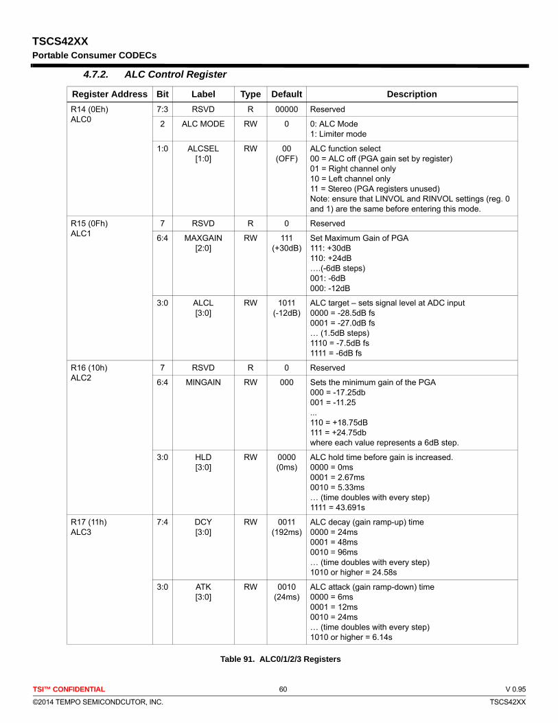
TSI™ CONFIDENTIAL 60 V 0.95
©2014 TEMPO SEMICONDCUTOR, INC. TSCS42XX
TSCS42XXPortable Consumer CODECs
4.7.2. ALC Control Register
Table 91. ALC0/1/2/3 Registers
Register Address Bit Label Type Default Description
R14 (0Eh)ALC0
7:3 RSVD R 00000 Reserved
2 ALC MODE RW 0 0: ALC Mode1: Limiter mode
1:0 ALCSEL[1:0]
RW 00(OFF)
ALC function select00 = ALC off (PGA gain set by register)01 = Right channel only10 = Left channel only11 = Stereo (PGA registers unused)Note: ensure that LINVOL and RINVOL settings (reg. 0 and 1) are the same before entering this mode.
R15 (0Fh)ALC1
7 RSVD R 0 Reserved
6:4 MAXGAIN[2:0]
RW 111(+30dB)
Set Maximum Gain of PGA111: +30dB110: +24dB….(-6dB steps)001: -6dB000: -12dB
3:0 ALCL[3:0]
RW 1011(-12dB)
ALC target – sets signal level at ADC input0000 = -28.5dB fs0001 = -27.0dB fs… (1.5dB steps)1110 = -7.5dB fs1111 = -6dB fs
R16 (10h)ALC2
7 RSVD R 0 Reserved
6:4 MINGAIN RW 000 Sets the minimum gain of the PGA000 = -17.25db001 = -11.25...110 = +18.75dB111 = +24.75dbwhere each value represents a 6dB step.
3:0 HLD[3:0]
RW 0000(0ms)
ALC hold time before gain is increased.0000 = 0ms0001 = 2.67ms0010 = 5.33ms… (time doubles with every step)1111 = 43.691s
R17 (11h)ALC3
7:4 DCY[3:0]
RW 0011(192ms)
ALC decay (gain ramp-up) time0000 = 24ms0001 = 48ms0010 = 96ms… (time doubles with every step)1010 or higher = 24.58s
3:0 ATK[3:0]
RW 0010(24ms)
ALC attack (gain ramp-down) time0000 = 6ms0001 = 12ms0010 = 24ms… (time doubles with every step)1010 or higher = 6.14s

TSI™ CONFIDENTIAL 61 V 0.95
©2014 TEMPO SEMICONDCUTOR, INC. TSCS42XX
TSCS42XXPortable Consumer CODECs
4.7.3. Peak Limiter
To prevent clipping, the ALC circuit also includes a limiter function. If the ADC input signal exceeds87.5% of full scale (–1.16dB), the PGA gain is ramped down at the maximum attack rate, until thesignal level falls below 87.5% of full scale. This function is automatically enabled whenever the ALCis enabled.
4.7.4. Input Threshold
To avoid hissing during quiet periods, the TSCS42XX has an input threshold noise gate function thatcompares the signal level at the inputs to a noise gate threshold. Below the threshold, the program-mable gain can be held , or the ADC output can be muted. The threshold can be adjusted in incre-ments of 1.5dB.
The noise gate activates when the signal-level at the input pin is less than the Noise Gate Threshold(NGTH) setting.
The ADC output can be muted. Alternatively, the PGA gain can be held .
The threshold is adjusted in 1.5dB steps. The noise gate only works in conjunction with the ALC, andalways operates on the same channel(s) as the ALC.
4.7.5. Noise Gate Control Register
Table 92. NGATE Register
4.8. Digital Microphone Support
Line Input 3 may be an analog line (mic) or digital microphone input depending on the part option.
The digital microphone interface permits connection of a digital microphone(s) to the CODEC via the DMIC_DAT, and DMIC_CLK 2-pin interface. DMIC_DAT is an input that carries individual channels of digital microphone data to the ADC. In the event that a single microphone is used, the data is ported to both ADC channels. This mode is selected using a control bit and the left time slot is copied to the ADC left and right inputs.
The DMIC_CLK output is synchronous to the internal master (DSP) clock and is adjustable in 4 steps. Each step provides a clock that is a multiple of the chosen ADC base rate and modulator rate.The default frequency is 320/3 times the ADC base rate for 32KHz, and 80 times the base rate for 44.1KHz and 48KHz base rates.
Register Address Bit Label Type Default Description
R12 (12h)NGATE
7:3 NGTH[4:0]
RW 00000 Noise gate threshold (compared to ADC full-scale range)00000 -76.5dBfs00001 -75dBfs… 1.5 dB steps11110 -31.5dBfs11111 -30dBfs
2:1 NGG[1:0]
RW 00 Noise gate typeX0 = PGA gain held constant01 = mute ADC output11 = reserved (do not use this setting)
0 NGAT RW 0 Noise gate function enable1 = enable0 = disable

TSI™ CONFIDENTIAL 62 V 0.95
©2014 TEMPO SEMICONDCUTOR, INC. TSCS42XX
TSCS42XXPortable Consumer CODECs
4.8.1. DMIC Clock
Table 93. DMIC Clock
The two DMIC data inputs are shown connected to the ADCs through the same multiplexors as the analog ports. Although the internal implementation is different between the analog ports and the digital microphones, the functionality is the same. In most cases, the default values for the DMIC clock rate and data sample phase will be appropriate and an audio driver will be able to configure and use the digital microphones exactly like an analog microphone.
To conserve power, the analog portion of the ADC will be turned off if the D-mic input is selected. When switching from the digital microphone to an analog input to the ADC, the analog portion of the ADC will be brought back to a full power state and allowed to stabilize before switching from the digital microphone to the analog input. This should take less than 10mS.
If the ADC path is powered down, the DMIC_CLK output will be driven low to place the DMIC element into a low power state. (Many digital microphones will enter a low power state if the clock input is held at a DC level or toggled at a slow rate.)
SDM Rate DMRate [1:0] Base Rate DSPCLK DMIC_CLK divisor
DMIC_CLK
Full 00 32 KHz 40.960 MHz 12 3.413333 MHz
44.1 KHz 56.448 MHz 16 3.528 MHz
48 KHz 61.440 MHz 16 3.84 MHz
01 32 KHz 40.960 MHz 16 2.56 Mhz
44.1 KHz 56.448 MHz 20 2.8224 MHz
48 KHz 61.440 MHz 20 3.072 MHz
10 32 KHz 40.960 MHz 20 2.048 Mhz
44.1 KHz 56.448 MHz 24 2.352 MHz
48 KHz 61.440 MHz 24 2.56 MHz
11 32 KHz 40.960 MHz 24 1.706667 Mhz
44.1 KHz 56.448 MHz 32 1.764 MHz
48 KHz 61.440 MHz 32 1.92 MHz
Half 00 32 KHz 40.960 MHz 16 2.56 MHz
44.1 KHz 56.448 MHz 16 3.528 MHz
48 KHz 61.440 MHz 16 3.84 MHz
01 32 KHz 40.960 MHz 24 1.706667 MHz
44.1 KHz 56.448 MHz 24 2.352 MHz
48 KHz 61.440 MHz 24 2.56 MHz
10 32 KHz 40.960 MHz 32 1.28 MHz
44.1 KHz 56.448 MHz 32 1.764 MHz
48 KHz 61.440 MHz 32 1.92 MHz
11 32 KHz 40.960 MHz 40 1.024 MHz
44.1 KHz 56.448 MHz 40 1.4112 MHz
48 KHz 61.440 MHz 40 1.536 MHz

TSI™ CONFIDENTIAL 63 V 0.95
©2014 TEMPO SEMICONDCUTOR, INC. TSCS42XX
TSCS42XXPortable Consumer CODECs
4.8.2. Digital Mic Configuration
The TSCS42XX codec supports the following digital microphone configurations:
Table 94. Valid Digital Mic Configuration
Figure 19. Single Digital Microphone (data is ported to both left and right channels
Digital Mics Data Sample Notes
0 N/A No Digital Microphones1 Single Edge When using a microphone that supports multiplexed operation (2-mics can
share a common data line), configure the microphone for “Left” and select mono operation.
“Left” D-mic data is used for ADC left and right channels.2 Double Edge External logic required to support sampling on a single Digital Mic pin channel
on rising edge and second Digital Mic right channel on falling edge of DMIC_CLK for those digital microphones that don’t support alternative clock edge (multiplexed output) capability.
DMIC_DAT
DMIC_CLK
RightChannel
LeftChannel
Valid Data Valid Data Valid Data
DMIC_DAT
DMIC_CLK
Single Line In
Pin On-Chip Multiplexer
Pin
DigitalMicrophone
On-ChipOff-ChipM
UX
Stereo Channels Output
STEREOADCPCM
DMIC_DAT
DMIC_CLK
Left & RightChannel
Valid DataValid Data Valid Data Valid Data
Single “Left” Microphone, DMIC input set to mono input mode.
Single Microphone not supporting multiplexed output.

TSI™ CONFIDENTIAL 64 V 0.95
©2014 TEMPO SEMICONDCUTOR, INC. TSCS42XX
TSCS42XXPortable Consumer CODECs
Figure 20. Stereo Digital Microphone Configuration
Note Some Digital Microphone Implementations support data on either edge, therefore, the external mux may not be required.
DMIC_DAT
DMIC_CLK
RightChannel
LeftChannel
ValidData R
ValidData L
ValidData R
ValidData L
ValidData R
DigitalMicrophones
DMIC_CLK
MU
X
Stereo Channels Output
Pin
Pin
ExternalMultiplexer
On-Chip Multiplexer
On-ChipOff-Chip
STEREOADCPCM
MU
X
DMIC_DAT

TSI™ CONFIDENTIAL 65 V 0.95
©2014 TEMPO SEMICONDCUTOR, INC. TSCS42XX
TSCS42XXPortable Consumer CODECs
5. DIGITAL AUDIO AND CONTROL INTERFACES
5.1. Data Interface
For digital audio data, the TSCS42XX uses six pins to input and output digital audio data.
• ADCDOUT: ADC data output
• ADCLRCLK: ADC data alignment clock
• ADCBCLK: Bit clock, for synchronization
• DACDIN: DAC data input
• DACLRCLK: DAC data alignment clock
• DACBCLK: Bit clock, for synchronizationThe clock signals ADCBCLK, ADCLRCLK, DACBCLK, and DACLRCK are outputs when the TSCS42XX operates as amaster; they are inputs when it is a slave. Four different data formats are supported:
• Left justified
• Right justified
• I2S
• PCM Bluetooth All of these modes are MSB first.
5.2. Master and Slave Mode Operation
The TSCS42XX can be used as either a master or slave device, selected by the MS Bit. When operating as a master,the TSCS42XX generates ADCBCLK, ADCLRCLK, DACBCLK and DACLRCLK and controls sequencing of the datatransfer the data pins. In slave mode, the TSCS42XX provides data aligned to clocks it receives.
Figure 21. Master mode
Figure 22. Slave mode
ADCBCLK
ADCLRCLK
ADCDOUT
DACBCLK
DACLRCLK
DACDIN
CODECDSP
ENCODER/DECODER
ADCBCLK
ADCLRCLK
ADCDOUT
DACBCLK
DACLRCLK
DACDIN
CODECDSP
ENCODER/DECODER
TSI™ CONFIDENTIAL 66 V 0.95
©2014 TEMPO SEMICONDCUTOR, INC. TSCS42XX
TSCS42XXPortable Consumer CODECs
5.3. Audio Data Formats
The TSCS42XX supports 4 common audio interface formats and programmable clocking that provides broad compat-ibility with DSPs, Consumer Audio and Video SOCs, FPGAs, handset chipsets, and many other products.
In all modes, depending on word length, BCLK frequency and sample rate, there may be unused BCLK cycles beforeeach LRCLK transition. If the converter word length is smaller than the number of clocks per sample in the frame thenthe DAC will ignore (truncate) the extra bits while the ADC will zero pad the output data. If the converter word lengthchosen is larger than the number of clocks available per sample in the frame, the ADC data will be truncated to fit theframe and the DAC data will be zero padded.
5.3.1. PCM Interface
PCM Mode is a time-division multiplexed format. The PCM interface operates in either slave or master mode. Data issampled on the falling edge of the bit clock and transmitted on the rising edge. A control bit selects between a delayedand non-delayed data timing relative to the start of the frame sync. The LRCLK is one bit clock long for a Short FrameSync and one slot wide for a Long Frame Sync. PCM mode supports mono and stereo formats

TSI™ CONFIDENTIAL 67 V 0.95
©2014 TEMPO SEMICONDCUTOR, INC. TSCS42XX
TSCS42XXPortable Consumer CODECs
.
Figure 23. PCM Audio Interface
PCM-DSHIFT=0
BCLK
LRCLK
nSDI / SDO
Word Length (WL)
1/fs
n- 1 n-2321
MSB LSB
nn- 1 n-2321
MSB LSB
1 BCLK1 BCLK
Falling Edge Can Occur Anywhere In This Area(
Left Channel Right Channel
BCLK
LRCLK
nSDI / SDO
Word Length (WL)
1/fs
n- 1 n-2321
MSB LSB
nn- 1 n-2321
MSB LSB
1 BCLK1
BCLK
Falling Edge Can Occur Anywhere In This Area
Left Channel Right Channel
(Stereo)
(Stereo)
BCLK
LRCLK
nSDI / SDO
Word Length (WL)
1/fs
n- 1 n-2321
MSB LSB
1 BCLK1 BCLK
Falling Edge Can Occur Anywhere In This Area
Mono Channel
(Mono)
BCLK
LRCLK
nSDI / SDO
Word Length (WL)
1/fs
n- 1 n-2321
MSB LSB
1 BCLK1
BCLK
Falling Edge Can Occur Anywhere In This Area(
Mono Channel
(Mono)
PCM-DSHIFT=0
PCM-DSHIFT=1
PCM-DSHIFT=1

TSI™ CONFIDENTIAL 68 V 0.95
©2014 TEMPO SEMICONDCUTOR, INC. TSCS42XX
TSCS42XXPortable Consumer CODECs
For digital audio data, the TSCS42XX uses below six pins for PCM audio interface.
• ADCDOUT: PCM data out
• ADCCLRCLK: ADC PCM data alignment
• ADCBCLK: ADC PCM Bit clock, for synchronization
• DACDIN: PCM data in
• DACLRCLK:DAC PCM data alignment
• DACBCLK: DAC PCM Bit clock, for synchronization
5.3.1.1. PCM control Registers
Table 96. ADCPCMCTL2 Register
Bit LabelRead/Write
Reset Value
Description
R195(C3h)ADCPCMCTL1
7:5 GAINCODE RW 0 PCM gain code to be sent
4 GAINENABLE RW 0PCM gain code enable-if 1, replace lsb bits of data if 0, normal mode
3 BDELAYO RW 0output Bit clock delay, 0 = data not delayed, 1 = data delayed.
2 PCMFL RW 0PCM Frame Length in master mode, 0 = 128 bits peer frame, 1 = 256 bits per frame
1 SLSYNC RW 0short-Long Frame Sync, 0 = one clock wide, 1 = one slot wide
0 R 0 Reserved
Table 95. ADCPCMCTL1 Register
Bit LabelRead/Write
Reset Value
Description
R196(C4h)ADCPCMCTL2
7 RSVD R 0 Reserved
6 PCMMOMP RW 0PCM mono output mode, 0- When number of slots = 1, select left data for slot0, 1-select left data for slot0 = 1, select right data for slot0.
5 PCMSOP RW 0Number of Active Slots per PCM Output Frame, 0 = one, 1 = two
4:3 PCMDSSPRW 0 PCM Data Slots Size, 00 = 16 bit, 01 =24 bit, 10 = 32
bit, 11=Reserved
2 R 0 Reserved
1 R 0 Reserved
0 R 0 Reserved

TSI™ CONFIDENTIAL 69 V 0.95
©2014 TEMPO SEMICONDCUTOR, INC. TSCS42XX
TSCS42XXPortable Consumer CODECs
Table 98. DACPCMCTL2 Register
5.3.2. Left Justified Audio Interface
In Left Justified mode, the MSB is available on the first rising edge of BCLK following a LRCLK transition. The other bitsare then transmitted in order. The LRCLK signal is high when left channel data is present and low when right channeldata is present.
Bit LabelRead/Write
Reset Value
Description
R197(C5h)DACPCMCTL1
7:5 R 0 Reserved
4 R 0 Reserved
3 BDELAYI RW 0Input Bit clock delay, 0 = data not delayed, 1 = data delayed.
2 PCMFL RW 0PCM Frame Length in master mode, 0 = 128 bits peer frame, 1 = 256 bits per frame
1 SLSYNC RW 0short-Long Frame Sync, 0 = one clock wide, 1 = one slot wide
0 R 0 Reserved
Table 97. DACPCMCTL1Register
Bit LabelRead/Write
Reset Value
Description
R198(C6h)DACPCMCTL2
7 PCMFORMAT RW 0 DAC input path set to PCM format if 1
6 PCMMIM RW 0PCM mono input mode, 0- When number of slots = 1, select left data for slot0, 1-select left data for slot0 = 1, select right data for slot0.
5 PCMSI RW 0Number of Active Slots per PCM Output Frame, 0 = one, 1 = two
4:3 PCMDSSRW 0 PCM Data Slots Size, 00 = 16 bit, 01 =24 bit, 10 = 32
bit, 11=Reserved
2 PCMSIGNEXTRW 0 Data is received in 13bit sign extended mode, left
shift by 3 and pad with 0s
1 PCM13MODERW 0 Data is received with un-used gain bits,
set these to 0
0 R 0 Reserved
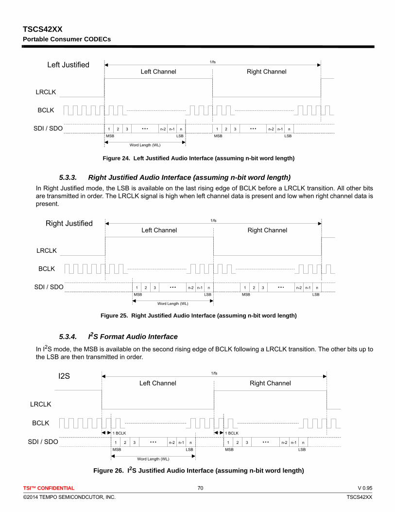
TSI™ CONFIDENTIAL 70 V 0.95
©2014 TEMPO SEMICONDCUTOR, INC. TSCS42XX
TSCS42XXPortable Consumer CODECs
Figure 24. Left Justified Audio Interface (assuming n-bit word length)
5.3.3. Right Justified Audio Interface (assuming n-bit word length)
In Right Justified mode, the LSB is available on the last rising edge of BCLK before a LRCLK transition. All other bitsare transmitted in order. The LRCLK signal is high when left channel data is present and low when right channel data ispresent.
Figure 25. Right Justified Audio Interface (assuming n-bit word length)
5.3.4. I2S Format Audio Interface
In I2S mode, the MSB is available on the second rising edge of BCLK following a LRCLK transition. The other bits up tothe LSB are then transmitted in order.
Figure 26. I2S Justified Audio Interface (assuming n-bit word length)
Left Justified
BCLK
LRCLK
nSDI / SDO
Left Channel Right Channel
Word Length (WL)
1/fs
n-1 n-2321
MSB LSB
nn-1 n-2321
MSB LSB
BCLK
LRCLK
nSDI / SDO
Left Channel Right Channel
Word Length (WL)
Right Justified 1/fs
n-1 n-2321
MSB LSB
nn-1 n-2321
MSB LSB
I2S
BCLK
LRCLK
nSDI / SDO
Left Channel Right Channel
Word Length (WL)
1/fs
n-1 n-2321
MSB LSB
nn-1 n-2321
MSB LSB
1 BCLK1 BCLK

TSI™ CONFIDENTIAL 71 V 0.95
©2014 TEMPO SEMICONDCUTOR, INC. TSCS42XX
TSCS42XXPortable Consumer CODECs
5.4. Audio Data Interface Registers
5.4.1. I2S Interface Control Registers
Table 99. AIC1 Register
5.4.2. Digital Mic Interface Control
Table 100. DMICCTL Register
Register Address Bit Label Default Description
R19(13h)AIC1
7 RESERVED 0h Reserved
6 BCLKINV 0hBCLK Invert (master and slave modes):1 = BCLK inverted0 = BCLK not inverted
5 MS 0hMaster/Slave Control: 0 = Slave; 1 = Master
4 LRP 0hLRClk Polarity:0 = Not inverted; 1 = Inverted
3:2 WL 2h
Audio Data Word Length: 0h = 16 bits; 1h = 20 bits; 2h = 24 bits; 3h = 32 bits
1:0 FORMAT 2h
Audio Data Format: 0h = Right justified; 1h = Left justified; 2h = I2S 3h = Reserved
Register Address Bit Label Type Default Description
R36 (24h)DMICCTL
7 DMicEn RW 0 Digital Microphone Enable0 = DMIC interface is disabled (DMIC_CLK low, DMIC muted)1 = DMIC interface is enabled
6:5 RSVD R 00 Reserved
4 DMono RW 0 0 = stereo operation, 1 = mono operation (left channel duplicated on right)
3:2 DMPhAdj[1:0] RW 00 Selects when the D-Mic data is latched relative to the DMIC_CLK.00 = Left data rising edge / right data falling edge01 = Left data center of high / right data center of low10 = Left data falling edge / right data rising edge11 = Left data center of low / right data center of high
1:0 DMRate[1:0] RW 00 Selects the DMIC clock rate: See table 93

TSI™ CONFIDENTIAL 72 V 0.95
©2014 TEMPO SEMICONDCUTOR, INC. TSCS42XX
TSCS42XXPortable Consumer CODECs
5.4.3. Audio Interface Output Tri-state
TRI is used to tri-state the ADCDOUT, ADCLRCLK, DACLRCLK, ADCBCLK, and DACBCLK pins. In Slave mode (MSbit=0) only ADCDOUT will be tri-stated since the other pins are configured as inputs. The Tri-stated pins are pulled lowwith an internal pull-down resistor unless that resistor is disabled.
5.4.4. Bit Clock and LR Clock Mode Controls
Although the DAC and ADC interfaces implement separate Bit Clock and LR Clock pins, it is also possible to share oneor both of the clocks.
the following restrictions must be observed when the BCLK from one path (DAC or ADC) is combined with the LRCLKfrom the other path (ADC or DAC) as described by the Bit Clock and LR Clock Mode Selection table below:
1. Both the DAC and ADC must be programmed for the same sample rate
2. Both the DAC and ADC must be programmed for the same number of clocks per frame
3. When in slave mode, the DAC and ADC data must be aligned relative to the provided BCLK and LRCLK (this is guaranteed in master mode)
4. The DAC and ADC must be powered down when changing the BLRCM mode
5. If sharing the BCLK from one path (DAC or ADC) and the LRCLK from the other path (ADC or DAC), shut down both the DAC and ADC before programming the sample rate and clocks per frame for either. (Again, both must match.)
Register Address Bit Label Type Default Description
R20 (14h)AIC2
7:6 DACDSEL[1:0] RW 00
00: left DAC = left I2S data; right DAC = right I2S data01: left DAC = left I2S data; right DAC = left I2S data10: left DAC = right I2S data; right DAC = right I2S data11: left DAC = right I2S data; right DAC = left I2S data
5:4 ADCDSEL[1:0] RW 00
00: left I2S data = left ADC; right I2S data = right ADC01: left I2S data = left ADC; right I2S data = left ADC10: left I2S data = right ADC; right I2S data = right ADC11: left I2S data = right ADC; right I2S data = left ADC
3 TRI RW 0
Tri-states ADCDOUT, ADCLRCLK, DACLRCLK, ADCBCLK, and DACBCLK pins.0 = ADCDOUT is an output, ADCLRCLK, DACLRCLK, ADCBCLK, and DACBCLK are inputs (slave mode) or outputs (master mode)1 = ADCDOUT, ADCLRCLK, DACLRCLK, ADCBCLK, and DACBCLK are high impedance
2:0 BLRCM[2:0] RW 000 Bitclock and LRClock mode. See Table Below
Table 101. AIC2 Register

TSI™ CONFIDENTIAL 73 V 0.95
©2014 TEMPO SEMICONDCUTOR, INC. TSCS42XX
TSCS42XXPortable Consumer CODECs
MSBLRCM
[2:0] MODE1
1.When sharing both the BCLK and LRCLK between the DAC and ADC interfaces, both the DAC and ADC must be programmedfor the same rate, the same number of clocks per frame, and data must be aligned the same with respect to LRCLK. Disableall converters before changing modes.
DACBCLK
ADCBCLK
DACLRCLK
ADCLRCLK
0 000 Independent Input for playback path input for record path Input for playback path input for record path
0 001 Independent Input for playback path input for record path Input for playback path input for record path
0 010Shared BCLK
(DAC)Input for playback and
recordunused Input for playback path input for record path
0 011Shared BCLK
& LRCLK (DAC)
Input for playback and record
unusedInput for playback and
recordunused
0 100
SharedBCLK (DAC)
& LRCLK (ADC)
Input for playback and record
unused unusedInput for playback and
record
0 101Shared BCLK
(ADC)unused
Input for playback and record
Input for playback path input for record path
0 110
SharedBCLK (ADC)
& LRCLK (DAC)
unusedInput for playback and
recordInput for playback and
recordunused
0 111Shared BCLK
& LRCLK (ADC)
unusedInput for playback and
recordunused
Input for playback and record
1 000Independent
(off if converter off)
Output for playback path (off when DACs off)2
2.DAC (playback path) is off when HPL, HPR, SPKL, and SPKR power states are off.
Output for record path(Off when ADC off)3
3.ADC is off when ADCL, and ADCR power states are off (PGA, D2S, Boost power states are not considered.)
Output for playback path (off when DACs
off)
Output for record path (off when ADCs off)
1 001Independent
(off if all converters off)
Output for playback path (off when DACs and
ADCs off)
Output for record path (off when DACs and
ADCs off)
Output for playback path (off when DACs
and ADCs off)
Output for record path (off when DACs and
ADCs off)
1 010Shared BCLK
(DAC)
Output for playback and record (stays on if either
DAC or ADC on)unused (off)
Output for playback path (Off if DAC is off)
Output for record path (off when ADCs off)
1 011Shared BCLK
& LRCLK (DAC)
Output for playback and record (stays on if either
DAC or ADC on)unused (off)
Output for playback and record (stays on if either DAC or ADC on)
unused (off)
1 100Shared
BCLK(DAC)&LRCLK(ADC)
Output for playback and record (stays on if either
DAC or ADC on)unused (off) unused (off)
Output for playback and record (stays on if either DAC or ADC on)
1 101Shared BCLK
(ADC)unused (off)
Output for playback and record (stays on if either
DAC or ADC on)
Output for playback path (Off if DAC is off)
Output for record path (off when ADCs off)
1 110Shared
BCLK(ADC)&LRCLK(DAC)
unused (off)Output for playback and record (stays on if either
DAC or ADC on)
Output for playback and record (stays on if either DAC or ADC on)
unused (off)
1 111Shared BCLK
& LRCLK(ADC)
unused (off)Output for playback and record (stays on if either
DAC or ADC on)unused (off)
Output for playback and record (stays on if either DAC or ADC on)
Table 102. Bit Clock and LR Clock Mode Selection
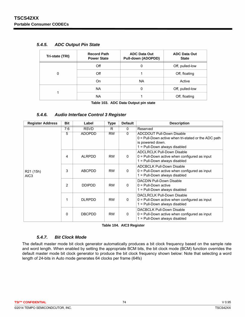
TSI™ CONFIDENTIAL 74 V 0.95
©2014 TEMPO SEMICONDCUTOR, INC. TSCS42XX
TSCS42XXPortable Consumer CODECs
5.4.5. ADC Output Pin State
5.4.6. Audio Interface Control 3 Register
5.4.7. Bit Clock Mode
The default master mode bit clock generator automatically produces a bit clock frequency based on the sample rateand word length. When enabled by setting the appropriate BCM bits, the bit clock mode (BCM) function overrides thedefault master mode bit clock generator to produce the bit clock frequency shown below: Note that selecting a wordlength of 24-bits in Auto mode generates 64 clocks per frame (64fs)
Tri-state (TRI)Record PathPower State
ADC Data Out Pull-down (ADOPDD)
ADC Data OutState
0
Off 0 Off, pulled-low
Off 1 Off, floating
On NA Active
1NA 0 Off, pulled-low
NA 1 Off, floating
Table 103. ADC Data Output pin state
Register Address Bit Label Type Default Description
R21 (15h)AIC3
7:6 RSVD R 0 Reserved5 ADOPDD RW 0 ADCDOUT Pull-Down Disable
0 = Pull-Down active when tri-stated or the ADC path is powered down.1 = Pull-Down always disabled
4 ALRPDD RW 0ADCLRCLK Pull-Down Disable0 = Pull-Down active when configured as input1 = Pull-Down always disabled
3 ABCPDD RW 0ADCBCLK Pull-Down Disable0 = Pull-Down active when configured as input1 = Pull-Down always disabled
2 DDIPDD RW 0DACDIN Pull-Down Disable0 = Pull-Down active1 = Pull-Down always disabled
1 DLRPDD RW 0DACLRCLK Pull-Down Disable0 = Pull-Down active when configured as input1 = Pull-Down always disabled
0 DBCPDD RW 0DACBCLK Pull-Down Disable0 = Pull-Down active when configured as input1 = Pull-Down always disabled
Table 104. AIC3 Register

TSI™ CONFIDENTIAL 75 V 0.95
©2014 TEMPO SEMICONDCUTOR, INC. TSCS42XX
TSCS42XXPortable Consumer CODECs
.
The BCM mode bit clock generator produces 16, 20, or 32 bit cycles per sample.
Figure 27. Bit Clock mode
Note: The clock cycles are evenly distributed throughout the frame (true multiple of LRCLK not a gated clock.)
5.5. I2C /Control Interface
The registers are accessed through a serial control interface using a multi-word protocol comprisedof 8-bit words. The first 8 bits provide the device address and Read/Write flag. In a write cycle, thenext 8 bits provide the register address; all subsequent words contain the data, corresponding to the8 bits in each control register.The control interface operates using a standard 2-wire interface, as aslave device only. The TSCS42XX has 8 bit device address E2 for Analog mic version of the partand D2 for Digital mic version of the part
5.5.1. Register Write Cycle
The controller indicates the start of data transfer with a high to low transition on SDA while SCLremains high, signalling that a device address and data will follow. All devices on the 2-wire busrespond to the start condition and shift in the next eight bits on SDIN (7-bit address + Read/Write bit,MSB first). If the device address received matches the address of the TSCS42XX and the R/W bit is‘0’, indicating a write, then the TSCS42XX responds by pulling SDA low on the next clock pulse(ACK); otherwise, the TSCS42XX returns to the idle condition to wait for a new start condition andvalid address.
Once the TSCS42XX has acknowledged a correct device address, the controller sends theTSCS42XX register address. The TSCS42XX acknowledges the register address by pulling SDAlow for one clock pulse (ACK). The controller then sends a byte of data (B7 to B0), and theTSCS42XX acknowledges again by pulling SDA low.
When there is a low to high transition on SDA while SCL is high, the transfer is complete. Afterreceiving a complete address and data sequence the TSCS42XX returns to the idle state. If a start orstop condition is detected out of sequence, the device returns to the idle condition.
Register Address Bit Label Type Default Description
R23/R25 (17h/19h)ADCSR/DACSR
7:6ABCM[1:0]DBCM[1:0]
RW 00
BCLK Frequency00 = Auto01 = 32 x fs10 = 40 x fs11 = 64 x fs
Table 105. ADCSR/ DACSR Register
Fs x 64
Fs x 40
LRCLK
Fs x 32

TSI™ CONFIDENTIAL 76 V 0.95
©2014 TEMPO SEMICONDCUTOR, INC. TSCS42XX
TSCS42XXPortable Consumer CODECs
Figure 28. 2-Wire Serial Control Interface
5.5.2. Multiple Write Cycle
The controller may write more than one register within a single write cycle. To write additional regis-ters, the controller will not generate a stop or start (repeated start) command after receiving theacknowledge for the second byte of information (register address and data). Instead the controllerwill continue to send bytes of data. After each byte of data is received, the register address is incre-mented.
Figure 29. Multiple Write Cycle
5.5.3. Register Read Cycle
The controller indicates the start of data transfer with a high to low transition on SDA while SCLremains high, signalling that a device address and data will follow. If the device address receivedmatches the address of the TSCS42XX and the R/W bit is ‘0’, indicating a write, then the TSCS42XXresponds by pulling SDA low on the next clock pulse (ACK); otherwise, the TSCS42XX returns to theidle condition to wait for a new start condition and valid address.
Once the TSCS42XX has acknowledged a correct address, the controller sends a restart command(high to low transition on SDA while SCL remains high). The controller then re-sends the devicesaddress with the R/W bit set to ‘1’ to indicate a read cycle.The TSCS42XX acknowledges by pullingSDA low for one clock pulse. The controller then receives a byte of register data (B7 to B0).
For a single byte transfer, the host controller will not acknowledge (high on data line) the data byteand generate a low to high transition on SDA while SCL is high, completing the transfer. If a start orstop condition is detected out of sequence, the device returns to the idle condition.
Figure 30. Read Cycle
nW
SCL
SDA Device Address DA[6:0]
START
ACK
Register Address RA[7:0] Register Data RD[7:0]
ACK ACK
STOP
nW
SCL
SDA Device Address DA[6:0]
START
ACK
Register Address RA[7:0] Register Data RD[7:0]
ACK ACK
STOP
ACK ACK
Register Write 1 Register Write 2 ...
Register Data RD[7:0]@RA[7:0]+1
Register Write n
Register Data RD[7:0]@RA[7:0]+n
nACK
SCL
SDA Device Address DA[6:0] nW
START
ACK
Register Address RA[7:0] Register Data RD[7:0]
ACK
STOP
Device Address DA[6:0] R
ACK
RESTART

TSI™ CONFIDENTIAL 77 V 0.95
©2014 TEMPO SEMICONDCUTOR, INC. TSCS42XX
TSCS42XXPortable Consumer CODECs
5.5.4. Multiple Read Cycle
The controller may read more than one register within a single read cycle. To read additional registers, the controllerwill not generate a stop or start (repeated start) command after sending the acknowledge for the byte of data. Insteadthe controller will continue to provide clocks and acknowledge after each byte of received data. The codec will automat-ically increment the internal register address after each register has had its data successfully read (ACK from host) butwill not increment the register address if the data is not received correctly by the host (nACK from host) or if the buscycle is terminated unexpectedly (however the EQ/Filter address will be incremented even if the register address is notincremented when performing EQ/Filter RAM reads). By automatically incrementing the internal register address aftereach byte is read, all the internal registers of the codec may be read in a single read cycle.
Figure 31. Multiple Read Cycle
5.5.5. Device Addressing and Identification
The TSCS42XX has a default slave address of D2. However, it is sometimes necessary to use a dif-ferent address. The TSCS42XX has a device address register for this purpose. The part itself has an8-bit Identification register and an 8-bit revision register that provide device specific information forsoftware. In addition, an 8-bit programmable subsystem ID register can allow firmware to provide adescriptive code to higher level software such as an operating system driver or application software.
5.5.6. Device Address Register
5.5.7. Device Identification Registers
Register Address Bit Label Type Default Description
R124 (7Ch)DEVADR
7:1 ADDR[7:1] RW 1101001 7-bit slave address
0 RSVD R 0
Table 106. DEVADRl Register
Register Address Bit Label Type Default Description
R126 (7Eh)DEVIDH
7:0 DID[15:8] R xxh16-bit device identification number. Contact TSI.
R125 (7Dh)DEVIDL
7:0 DID[7:0] R xxh
Table 107. DEVID H&L Registers
DA[6:0] nW ACK RA[7:0] RD[7:0]ACK ACK nACKDA[6:0] R ACKSrS P
Set Register Address Read Register @ RA[7:0]
RD[7:0]
Read Register @ RA[7:0] + 1
ACK RD[7:0]
Read Register @ RA[7:0] + n

TSI™ CONFIDENTIAL 78 V 0.95
©2014 TEMPO SEMICONDCUTOR, INC. TSCS42XX
TSCS42XXPortable Consumer CODECs
5.5.8. Device Revision Register
5.5.9. Register Reset
The TSCS42XX registers may be reset to their default values using the reset register. Writing a spe-cial, non-zero value to this register causes all other registers to assume their default states. Devicestatus bits will not necessarily change their values depending on the state of the device.
Register Address Bit Label Type Default Description
R127 (7Fh)REVID
7:4 MAJ[3:0] R xh 4-bit major revision number. Contact TSI.
3:0 MNR[3:0] R xh 4-bit minor revision number. Contact TSI.
Table 108. REVID Register
Register Address Bit Label Type Default Description
R128 (80h)RESET
7:0 Reset[7:0] RW 00hReset registerWriting a value of 85h will cause registers to assume their default values. Reading this register returns 00h
Table 109. RESET Register

TSI™ CONFIDENTIAL 79 V 0.95
©2014 TEMPO SEMICONDCUTOR, INC. TSCS42XX
TSCS42XXPortable Consumer CODECs
6. GPIO’S
Two GPIO’s are available on the GPIO1-GPIO0 pins. These GPIO pins are accessed via register bits. The general-pur-pose input/output (GPIO) pins can be used as either inputs or outputs. These pins are readable and can be set or read through the control interface. These pins are useful for interfacing to external hardware.
6.1. GPIO Usage Summary
6.2. GPIO Control Registers
6.2.1. GPIO Control 1 Register
Table 111. GPIOCTL1 Register
GPIO Pin Function 1 Function 2Pull-Up
Pull-Down
GPIO0GPIO0 Register Bit
RSVD Pull-Up
GPIO1GPIO1 Register Bit
RSVD Pull-Up
Table 110. GPIO Pin Usage Summary
Register Address Bit Label Type Default Description
Reg192 (C0h)GPIOCTL1
7 RESERVED R 0 Reserved
6 RESERVED R 0 Reserved
5 GPIO1CFG RW 0GPIO1 Configuration0 = GPIO1 Configured as Input/Output1 = GPIO1 Configured as Interrupt
4 GPIO0CFG RW 0GPIO0 Configuration0 = GPIO0 Configured as Input/Output1 = GPIO0 Configured as Interrupt
3 RESERVED R 0 Reserved
2 RESERVED R 0 Reserved
1 GPIO1DIR RW 0GPIO1 Input/Output0 = GPIO1 configured as input1 = GPIO1 configured as output
0 GPIO0DIR RW 0GPIO0 Input/Output0 = GPIO0 configured as input1 = GPIO0 configured as output

TSI™ CONFIDENTIAL 80 V 0.95
©2014 TEMPO SEMICONDCUTOR, INC. TSCS42XX
TSCS42XXPortable Consumer CODECs
6.2.2. GPIO Control 2 Register
Table 112. GPIOCTL2 Register
Register Address Bit Label Type Default Description
Reg 193 (C1h)GPIOCTL2
7:2 RESERVED R 0 Reserved
1 GPIO1PU R 0GPIO1 Pull up0 = GPIO1 pull up enabled1 = GPIO1 pull up disenabled
0 GPIO0PU R 0GPIO0 Pull up0 = GPIO0 pull up enabled1 = GPIO0 pull up disenabled

TSI™ CONFIDENTIAL 81 V 0.95
©2014 TEMPO SEMICONDCUTOR, INC. TSCS42XX
TSCS42XXPortable Consumer CODECs
7.CLOCK GENERATION
The TSCS42XX uses two PLL to generate two high frequency reference clocks. The clock frequencies of each refer-ence clock are based on multiples of 44.1KHz and 48KHz sample rates.The clock source for the PLL’s can be theXTAL input, MCLK1 input via the XTAL_IN pin, the MCLK2 pin, or one of the I2S interface BCLK inputs. Each PLL canbe independently powered down if the audio sample rates generated by that particular PLL are not required.
7.1. On-Chip PLLs
The TSCS42XX generates two high-quality, high-frequency clocks122.880MHz and 112.896MHz. The PLL’s support awide range of input clock frequencies. Some typical frequencies are 19.2Mhz, 22MHz, 22.5792MHz, 24MHz, 24.576MHz, 27MHz, and 36MHz. It should be noted that some input clock frequencies may not result in being able to gener-ate the 122.880MHz and 112.896Mhz clocks exactly resulting in an error in the audio sample rate.
Audio Clocks - Each PLL generates one of two clock frequencies based on two audio sample rates.
122.880 MHz (2560 x 48 KHz)112.896 MHz (2560 x 44.1 KHz)
It is important that the crystal oscillator and needed PLLs remain on until all audio functions, including jack detection,are disabled.
Figure 32. PLL Block Diagram
Reference Divider Output
Divider
FeedbackDivider
VCO
PHASE
InputClock Output
Clock
PLL

TSI™ CONFIDENTIAL 82 V 0.95
©2014 TEMPO SEMICONDCUTOR, INC. TSCS42XX
TSCS42XXPortable Consumer CODECs
Figure 33. System Clock Diagram
7.2. System Clock Generation
The TSCS42XX supports an internal clock and audio sample rate that is selectable between 11.025KHz, 12 KHz, 22.050KHz, 24KHz, 44.1KHz, 48KHz, 88.2KHz, and 96KHz. One bi-directional stereo I2S interfaces is available. In Master mode an internal timing generator is used to specify the audio sample rate. The sample rate specified in Master mode is independent from the internal clock rate.and the specified range is 8KHz to 96KHz. A variety of sample rates based on 44.1K, 48K and 32K are supported. A highly programmable PLL enables just about any input frequency to be used.
7.2.1 PLL Dividers
The chosen input frequency is multiplied up by the PLL’s to generate the required output frequencies; 122.88MHz and 112.896MHz. It should be noted that it may not always be possible to generate the required output frequencies with zero error. Some values for the PLL dividers relative a specific input frequency are shown in the table below.
PLL1
PLL1 (122.88M)PDB r0x61 d1 (1)
Internal 48K rate clock (122.88M)
OUTDIV PLL1r0x4F d7:0 (01h)
REFDIV PLL1r0x4E d7:0 (14h)
FBDIV PLL1MSB r0x51 d2:0 (0h)LSB r0x50 d7:0 (C8h)
PLL2 (112.896M)PDB r0x61 d2 (1)
Internal 44.1K rate clock (112.896M)
OUTDIV PLL2r0x54 d7:0 (01h)
REFDIV PLL2r0x53 d7:0 (10h)
FBDIV PLL2MSB r0x56 d2:0 (0h)LSB r0x55 d7:0 (93h)
PLL2
Default 12.288MHz XTAL
Default 12.288MHz XTAL
PLL2 112.896MHz
PLL1 122.88MHz
Optional tuning caps
XTAL OSC/Clock Buffer
XTAL_IN/MCLK1
XTAL_OUT
Clock or Crystal Input (22.5792M, 24.576M, 27M, 36M)
XTAL_IN
MCLK1
112.896 MHz Audio Clock
122.88 MHz Audio Clock
XTAL_INMCLK1
DACBCLKADCBCLK
MCLK2
PLL2
MUX
XTAL_INMCLK1
DACBCLKADCBCLK
MCLK2
PLL1
MUX
MCLK2MCLK2
DACBCLKDACBCLK
ADCBCLKADCBCLK

TSI™ CONFIDENTIAL 83 V 0.95
©2014 TEMPO SEMICONDCUTOR, INC. TSCS42XX
TSCS42XXPortable Consumer CODECs
Table 113. Typical PLL Divider Value
OUTPUT FREQUENCYXtal Input TimeBase PLL1 Default Power (122.88MHz) PLL2 Default Power (112.896MHz)
MHz 77h 52h 60h 4Eh 4Fh 50h 51h Fvco 57h 60h 53h 54h 55h 56h Fvco
0.51200 0x01 0x22 0x04 0x01 0x03 0xD0 0x02 368.64 0x1B 0x10 0x01 0x04 0x72 0x03 451.58
0.70560 0x02 0x22 0x04 0x02 0x03 0x15 0x04 368.68 0x22 0x10 0x01 0x04 0x80 0x02 451.58
1.02400 0x03 0x22 0x04 0x02 0x03 0xD0 0x02 368.64 0x1B 0x10 0x02 0x04 0x72 0x03 451.58
1.41120 0x05 0x39 0x04 0x07 0x02 0xC3 0x04 245.75 0x1B 0x10 0x03 0x03 0xD0 0x02 338.69
1.53600 0x05 0x1A 0x04 0x02 0x03 0xE0 0x01 368.64 0x1A 0x10 0x02 0x03 0xB9 0x01 338.69
2.04800 0x07 0x22 0x04 0x04 0x03 0xD0 0x02 368.64 0x1B 0x10 0x04 0x04 0x72 0x03 451.58
2.40000 0x08 0x22 0x04 0x05 0x03 0x00 0x03 368.64 0x23 0x10 0x05 0x05 0x98 0x04 564.48
2.82240 0x0A 0x23 0x04 0x07 0x04 0xC3 0x04 491.5 0x22 0x10 0x05 0x03 0x58 0x02 338.69
3.07200 0x0B 0x22 0x04 0x07 0x03 0x48 0x03 368.64 0x1A 0x10 0x04 0x03 0xB9 0x01 338.69
5.64480 0x15 0x23 0x04 0x0E 0x04 0xC3 0x04 491.5 0x1A 0x10 0x08 0x03 0xE0 0x01 338.69
6.14400 0x17 0x1A 0x04 0x08 0x03 0xE0 0x01 368.64 0x1A 0x10 0x08 0x03 0xB9 0x01 338.69
12.00000 0x2E 0x1B 0x04 0x19 0x03 0x00 0x03 368.64 0x2A 0x10 0x19 0x05 0x98 0x04 564.48
12.28800 0x2F 0x1A 0x04 0x12 0x03 0x1C 0x02 368.64 0x22 0x10 0x20 0x03 0x72 0x03 338.69
19.20000 0x4A 0x13 0x04 0x14 0x03 0x80 0x01 368.64 0x1A 0x10 0x19 0x03 0xB9 0x01 338.69
22.00000 0x55 0x2A 0x04 0x37 0x05 0x00 0x06 614.4 0x22 0x10 0x26 0x03 0x49 0x02 338.68
22.57920 0x57 0x22 0x04 0x31 0x03 0x20 0x03 368.64 0x1A 0x10 0x1D 0x03 0xB3 0x01 338.69
24.00000 0x5D 0x13 0x04 0x19 0x03 0x80 0x01 368.64 0x1B 0x10 0x19 0x05 0x4C 0x02 564.48
24.57600 0x5F 0x13 0x04 0x1D 0x03 0xB3 0x01 368.64 0x22 0x10 0x40 0x03 0x72 0x03 338.69
25.00000 0x61 0x1B 0x04 0x37 0x03 0x2B 0x03 368.64 0x1A 0x10 0x2A 0x03 0x39 0x02 338.69
26.00000 0x65 0x23 0x04 0x41 0x05 0x00 0x06 614.4 0x1A 0x10 0x26 0x03 0xEF 0x01 338.68
27.00000 0x68 0x22 0x04 0x4B 0x03 0x00 0x04 368.64 0x2A 0x10 0x7D 0x03 0x20 0x06 338.69
36.00000 0x8C 0x1B 0x04 0x4B 0x03 0x00 0x03 368.64 0x2A 0x10 0x7D 0x03 0x98 0x04 338.69
40.00000 0x9B 0x22 0x08 0x7D 0x03 0x80 0x04 368.64 0x23 0x10 0x7D 0x05 0xE4 0x06 564.48

TSI™ CONFIDENTIAL 84 V 0.95
©2014 TEMPO SEMICONDCUTOR, INC. TSCS42XX
TSCS42XXPortable Consumer CODECs
Figure 34. Simplified System Clock Block Diagram
7.2.1.1. PLL Control Register
7.2.1.2. PLL Status Register
Register Address Bit Label Type Default Description
R96(60h)PLLCTL1B
7:6 RSVD R 0h Reserved
5:4 VCOI_PLL2 RW 1h PLL2 VCO/ICO current setting
3:2 VCOI_PLL1 RW 1h PLL1 VCO/ICO current setting
1:0 RSVD R 0h Reserved
Table 114. PLLCTL1B Register
Register Address Bit Label Type Default Description
R142(8Eh)PLLCTL0
7:2 RSVD R 00h Reserved
1 PLL2LK R 0h 1 = PLL2 has obtained lock
0 PLL1LK R 0h 1 = PLL1 has obtained lock
Table 115. PLLCTL0 Register
DSP
SDOUT1
DAC
SPKR AMP
HP
CLK2
CLK1MCLK1
XTAL PLL2
PLL1DIV
ADC/DMIC
ICLKGEN
SDIN1
LRCLK#/BCLK# PORT#CLKGEN
2
MCLK2BCLK
2

TSI™ CONFIDENTIAL 85 V 0.95
©2014 TEMPO SEMICONDCUTOR, INC. TSCS42XX
TSCS42XXPortable Consumer CODECs
7.2.1.3. PLL Reference Register
7.2.1.4. PLL1 Control Register
7.2.1.5.PLL1 Reference Clock Divider Register
7.2.1.6.PLL1 Output Divider Register
7.2.1.7.PLL1 Feedback Divider Low Register
Register Address Bit Label Type Default Description
R143(8Fh)PLLREFSEL
7 RSVD R 0h Reserved
6:4 PLL2_REF_SEL RW 0hPLL2 Reference Mux, 000 = xtal_in/mclk1; 001 = mclk2; 010 = dac_bclk; 011 = adc_bclk; 100 = pll1 output; 101 - 111 = reserved
3 RSVD R 0h Reserved
2:0 PLL1_REF_SEL RW 0hPLL1 Reference Mux, 000 = xtal_in/mclk1; 001 = mclk2; 010 = dac_bclk; 011 = adc_bclk; 100 = pll2 output; 101 - 111 = reserved
Table 116. PLLREFSEL Register
Register Address Bit Label Type Default Description
R82(52h)PLLCTLD
7:5 RSVD R 0 Reserved
4:3 RZ_PLL1 RW 3h PLL1 Zero R setting
2:0 CP_PLL1 RW 2h PLL1 main charge pump current setting
Table 117. PLLCTLD Register
Register Address Bit Label Type Default Description
R78(4Eh)PLLCTL9
7:0 REFDIV_PLL1 RW 19h PLL1 refclk divider
Table 118. PLLCTL9 Register
Register Address Bit Label Type Default Description
R79(4Fh)PLLCTLA
7:0 OUTDIV_PLL1 RW 03h PLL1 output divider
Table 119. PLLCTLA Register
Register Address Bit Label Type Default Description
R80(50h)PLLCTLB
7:0 FBDIVL_PLL1 RW 80hPLL1 feedback divider
Table 120. PLLCTLB Register

TSI™ CONFIDENTIAL 86 V 0.95
©2014 TEMPO SEMICONDCUTOR, INC. TSCS42XX
TSCS42XXPortable Consumer CODECs
7.2.1.8. PLL1 Feedback Divider High Register
7.2.1.9.PLL2 Control Register
7.2.1.10.PLL2 Reference Clock Divider Register
7.2.1.11.PLL2 Output Divider Register
7.2.1.12.PLL2 Feedback Divider Low Register
7.2.1.13.PLL2 Feedback Divider High Register
Register Address Bit Label Type Default Description
R81(51h)PLLCTLC
7:3 RSVD R 0 Reserved
2:0 FBDIVH_PLL1 RW 1h PLL1 feedback divider
Table 121. PLLCTLC Register
Register Address Bit Label Type Default Description
R87(57h)PLLCTL12
7:6 R 0 Reserved
5:3 RZ_PLL2 RW 3h PLL2 Zero R setting
2:0 CP_PLL2 RW 2h PLL2 main charge pump current setting
Table 122. PLLCTL12 Register
Register Address Bit Label Type Default Description
R83(53h)PLLCTLE
7:0 REFDIV_PLL2 RW 12hPLL2 reference clock divider
Table 123. PLLCTLE Register
Register Address Bit Label Type Default Description
R84(54h)PLLCTLEF
7:0 OUTDIV_PLL2 RW 03h PLL2 output divider
Table 124. PLLCTLF Register
Register Address Bit Label Type Default Description
R85(55h)PLLCTL10
7:0 FBDIVL_PLL2 RW 1ch PLL2 feedback low divider
Table 125. PLLCTL10 Register
Register Address Bit Label Type Default Description
R86(56h)PLLCTL11
7:3 RSVD R 0 Reserved
2:0 FBDIVH_PLL2 RW 2h PLL2 feedback high divider
Table 126. PLLCTL11 Register

TSI™ CONFIDENTIAL 87 V 0.95
©2014 TEMPO SEMICONDCUTOR, INC. TSCS42XX
TSCS42XXPortable Consumer CODECs
7.2.1.14.PLL Pwer DownControl Register
7.2.2 PLL Power Down Control
Each PLL can be powered down to save power if only one set of base audio rates is required. The base audio rates are defined as 44.1KHz based rates or 48KHz based rates. If support for either 44.1KHz or 48KHz based rates is not needed then the PLL associated with the unused rate can be powered down.
7.2.3 Audio Clock Generation
Figure 33 shows the simplified block diagram. The TSCS42XX utilizes internal PLLs to generate the PLL clocks at 112.896 MHz (22.5792MHz *5) and122.880 MHz (24.576 *5). Intermediate clocks (61.44MHz, 40.96MHz, 56.448MHz) are then generated which are then used to generate the audio sample rates. There is one internal clock rate that can be specified to operate at 11.025KHz, 12 KHz, 22.050KHz, 24KHz, 44.1KHz, 48KHz,88.2KHz, and 96KHz. When changing sample rates a delay of up to 5mS may be needed for the part to properly lock PLLs, flush filters, etc.
7.2.3.1.PLL Clock Source
The clock source for the PLL can be selected from the XTAL input, MCLK1 input via the XTAL_IN pin, the MCLK2 pin or one of the I2S BCLK inputs via a selectable mux.
Register Address Bit Label Type Default Description
R97(61h)PLLCTL1C
7:3 RESERVED R 0h Reserved
2 PDB_PLL2 RW 0hPLL2 Power Down: 1 = Power Up0 = Power Down
1 PDB_PLL1 RW 0hPLL1Power down1 = Power Up0 = Power Down
0 RESERVED R 0h Reserved
Table 127. PLLCTL1C Register

TSI™ CONFIDENTIAL 88 V 0.95
©2014 TEMPO SEMICONDCUTOR, INC. TSCS42XX
TSCS42XXPortable Consumer CODECs
7.2.3.2. Internal Sample Rate Control Register
These register define the internal sample rate.
Table 129. DACSR Register
Register Address Bit Label Default Description
R23(17h)ADCSR
7:6 ABCM 0h
ADC bit Clock Mode (for ADCBCLK generation in master mode):0h=Auto1h = 32x Fs2h = 40x Fs3h = 64x Fs
5 RSVD 0h Reserved
4:3 ABR 2h
ADC Base Rate0h = 32kHz1h = 44.1kHz2h = 48KHz3h = Reserved
2:0 ABM 2h
ADC Base Rate Multiplier0h = 0.25x1h = 0.5x2h = 1x3h = 2x4h-7h = Reserved
Table 128. ADCSR Register
Register Address Bit Label Default Description
R25 (19h)DACSR
7:6 DBCM 0h
DAC bit Clock Mode (for DACBCLK generation in master mode):0h=Auto1h = 32x Fs2h = 40x Fs3h = 64x Fs
5 RSVD 0h Reserved
4:3 DBR 2h
DAC Base Rate0h = 32kHz1h = 44.1kHz2h = 48KHz3h = Reserved
2:0 DBM 2h
DAC Base Rate Multiplier0h = 0.25x1h = 0.5x2h = 1x3h = 2x4h-7h = Reserved

TSI™ CONFIDENTIAL 89 V 0.95
©2014 TEMPO SEMICONDCUTOR, INC. TSCS42XX
TSCS42XXPortable Consumer CODECs
Internal Sample Rates
Table 130. DAC/ADC Sample rates
7.2.3.3. MCLK2 Pin
The MCLK2 pin is configured to be an input and can provide a clock to drive the input to the PLLs or the I2S MasterMode clock generators.
7.2.3.4. I2S Master Mode Clock Generation
I2S input audio source can operate as a timing Slave or Master. When operated in Master Mode an internal clock gen-erator is used to produce the required bit and frame clocks to be driven out of the LRCLK and BCLK pins of each inputI2S interface. The clock source for the I2S master clock generation can be selected between the PLL generated inter-nal timing or an externally supplied clock via the MCLK2 input.
7.2.3.5. I2S Master Mode Sample Rate Control
TI2S slave or master mode is set in register 13 MS bit. The I2S BR bits set the base audio sample to be either 44.1Khzor 48KHz. The I2S BM bits are then used to set the base rate multiplier ratio. The I2S BCM bits set the BCLK ratio vssample rate. The I2S BR, BM and BCM bits are located in register 17h for the ADC while register 19h for the DAC.
7.2.3.6. DAC/ADC Clock Control
The power consumption and audio quality may be adjusted by changing the converter modulator rate. By default theDAC and ADC Sigma-Delta modulators run at a high rate for the best audio quality. The modulator rates for the con-verters may be forced to run at half their nominal rate to conserve power. A third option allows the modulator rate toautomatically drop to half rate when low sampling rates are chosen (1/2 or 1/4 the base rate.) The DACs and ADCs areindependently controlled
xBR [4:3] xBM [2:0] BASE RATE SAMPLE RATE
00
000
40.96MHz
8kHz(MCLK/5120)
001 16kHz(MCLK/2560)
010 32 kHz (MCLK/1280)
011 64kHz (MCLK/640)
01
000
56.448MHz
11.025kHz(MCLK/5120)
001 22.050kHz(MCLK/2560)
010 44.1 kHz (MCLK/1280)
011 88.2 kHz (MCLK/640)
10
000
61.44 MHz
12kHz(MCLK/5120)
001 24kHz(MCLK/2560)
010 48 kHz (MCLK/1280)
011 96 kHz (MCLK/640)

TSI™ CONFIDENTIAL 90 V 0.95
©2014 TEMPO SEMICONDCUTOR, INC. TSCS42XX
TSCS42XXPortable Consumer CODECs
Register Address Bit Label Type Default Description
R31(1Fh)CONFIG0
7:6 ASDM[1:0] RW 2h
ADC Modulator Rate00b = Reserved01b = Half10b = Full11b = Auto
5:4 DSDM[1:0] RW 2h
DAC Modulator Rate00b = Reserved01b = Half10b = Full11b = Auto
3:2 RSVD R 0 Reserved
1 DC_BYPASS RW 0h DAC DC Filter Bypass:0 = Filter enable1 = Filter bypassed
0 SD_FORCE_ON RW 0h Supply Detect Force On:0 = Supply detect not forced on1 = Supply detect forced on
NoteIf not forced on, the supply detect logic will automatically be enabled when features that use it are enabled (COP,UVLO)
Table 131. CONFIG0 Register

TSI™ CONFIDENTIAL 91 V 0.95
©2014 TEMPO SEMICONDCUTOR, INC. TSCS42XX
TSCS42XXPortable Consumer CODECs
Table 132. ADC and DAC Modulator Rates
7.2.3.7. Timebase Register
DSDM[1:0]ASDM[1:0]
BM [2:0] Modulator Rate
00 NA Reserved
01
000 (1/4x)
Half001 (1/2x)
010 (1x)
011 (2x)
10
000 (1/4x)
Full001 (1/2x)
010 (1x)
011 (2x)
11
000 (1/4x) Auto (Half)
001 (1/2x) Auto (Half)
010 (1x) Auto (Full)
011 (2x) Auto (Full)
Register Address Bit Label Type Default Description
R119(77h)TMBASE
7-0 TIMEBASE[7:0] RW 2FInternal Time Base Divider. This value should be programmed as [round(ref clock/256000)]-1
Table 133. TIMEBASE Register

TSI™ CONFIDENTIAL 92 V 0.95
©2014 TEMPO SEMICONDCUTOR, INC. TSCS42XX
TSCS42XXPortable Consumer CODECs
8. CHARACTERISTICS
8.1. Electrical Specifications
8.1.1. Absolute Maximum Ratings
Stresses above the ratings listed below can cause permanent damage to the TSCS42XX. These rat-ings, which are standard values for TSI commercially rated parts, are stress ratings only. Functionaloperation of the device at these or any other conditions above those indicated in the operational sec-tions of the specifications is not implied. Exposure to absolute maximum rating conditions forextended periods can affect product reliability. Electrical parameters are guaranteed only over therecommended operating temperature range.
8.1.2. Recommended Operating Conditions
Item Maximum Rating
Voltage on any pin relative to Ground Vss - 0.3V TO Vdd + 0.3V
Operating Temperature 0 oC TO 70 oC
Storage Temperature -55 oC TO +125 oC
Soldering Temperature 260 oC
MICBias Output Current 3mA
Amplifier Maximum Supply Voltage 6 Volts = PVDD
Audio Maximum Supply Voltage 3 Volts = AVDD/CPVDD
Digital I/O Maximum Supply Voltage 3.6 Volts = DVDD_IO
Digital Core Maximum Supply Voltage 2.0 Volts = DVDD
Table 134. Electrical Specification: Maximum Ratings
Parameter Min. Typ. Max. Units
Power Supplies DVDD_Core 1.4 2.0 V
DVDD_IO 1.4 3.5
AVDD/CPVDD 1.7 2.0
PVDD 3.0 5.5 V
Ambient Operating Temperature Analog - 5 V 0 25 70 oC
Case Temperature Tcase 90 oC
Table 135. Recommended Operating Conditions
ESD: The TSCS42XX is an ESD (electrostatic discharge) sensitive device. The human body and test equipment can accumulate and discharge electrostatic charges up to 4000 Volts without detection. Even though the TSCS42XX implements
internal ESD protection circuitry, proper ESD precautions should be followed to avoid damaging the functionality or performance.

TSI™ CONFIDENTIAL 93 V 0.95
©2014 TEMPO SEMICONDCUTOR, INC. TSCS42XX
TSCS42XXPortable Consumer CODECs
8.2. Device Characteristics
(Tambient = 25 ºC, DVDD_CORE=DVDD_IO=AVDD=1.9V, PVDD=3.6V, 997Hz signal, fs=48KHz, Input Gain=0dB, 24-bit audio)
Parameter Symbol Test Conditions Min Typ Max Unit
Analog Inputs (LIN1, LIN2, LIN3, RIN1, RIN2, RIN3)
Full Scale Input Voltage VFSIV
L/RIN1,2,3 Single Ended0.5-6
VrmsdBV
L/RIN1,2,3 Differential Mic0.5-6
VrmsdBV
Input Impedance 50 Kohm
Input Capacitance 10 pF
Analog Input Boost Amplifier
Programmable Gain Min 0.0 dB
Programmable Gain Max 30.0 dB
Programmable Gain Step Size 10.0 dB
Analog Input PGA
Programmable Gain Min -17.25 dB
Programmable Gain Max 30.0 dB
Programmable Gain Step Size Guaranteed Monotonic 0.75 dB
Digital Volume Control Amplifier
Programmable Gain Min -97 dB
Programmable Gain Max 30.0 dB
Programmable Gain Step Size Guaranteed Monotonic 0.5 dB
Mute Attenuation -999 dB
Analog Inputs (LIN1/RIN1, LIN2/RIN2 Differential) to ADC
Signal To Noise Ratio SNR A-weighted 20-20KHz 90 dB
Total Harmonic Distortion + Noise
THD+N -1dBFS input-800.01
dB%
Analog Inputs (LIN1, LIN2, LIN3, RIN1, RIN2, RIN3 Single Ended) to ADC
Signal To Noise Ratio SNR A-weighted 20-20KHz 90 dB
Total Harmonic Distortion + Noise
THD+N -1dBFS input-800.01
dB%
ADC channel Separation 997Hz full scale signal 70 dB
Channel Matching 997Hz signal 2 %
DAC to Line-Out (HPL, HPR with 10K / 50pF load)
Signal to Noise Ratio1 SNR A-weighted 102 dB
Total Harmonic Distortion +Noise2
THD+N 997Hz full scale signal -84 dB
Channel Separation 997Hz full scale signal 70 dB
Mute attenuation -999 dB
Headphone Outputs (HPL, HPR)
Full Scale Output Level VFSOVRL = 10Kohm 1.0 Vrms
RL = 16ohm 0.75 Vrms
Output Power PO997Hz full scale signal, RL = 16ohm
35 mW (ave)
Signal to Noise Ratio SNR A-weighted, RL = 16ohm 102 dB
Table 136. Device Characteristics

TSI™ CONFIDENTIAL 94 V 0.95
©2014 TEMPO SEMICONDCUTOR, INC. TSCS42XX
TSCS42XXPortable Consumer CODECs
Total Harmonic Distortion +Noise
THD+NRL = 16ohms, -3dBFS -76 dB
RL = 32ohms, -3dBFS -78 dB
Speaker Outputs (L+, L-, R+, R- with 8ohms bridge-tied load)
Full Scale Output Level VFSOVPVDD=5VPVDD=3.6V
3.02.1
Vrms
Output Power PO
997Hz full scale signal, output power mode disabledPVDD=5V, 8ohmPVDD=3.6V, 8ohm
1.57
W(ave)
PVDD = 5V, 4 ohmDIDD = 3.6V, 4 ohm
31.4
W(ave)
Signal to Noise Ratio SNR A-weighted 90 dB
Total Harmonic Distortion + Noise
THD+N 5V/8ohms/0.5W 0.05 %
Speaker Supply Leakage Current
IPVDD 1 uA
Efficiency hPVDD=3.6V RL=8,PO = 0.5WPVDD=5V RL=8,PO = 1W
92 %
Analog Voltage Reference Levels
Charge Pump Output V- -5%-AVDD
+100mV+5% V
Microphone Bias
Bias Voltage VMICBIAS - 2.5 - V
BIAS current Source 3 mA
Power Supply Rejection Ratio PSRRMICBIAS3.3V<PVDD<5.25V 80 dB
3.0V<PVDD<3.3V 40 dB
Digital Input/Output
ADC/DAC BCLK input rate Fmax 30 MHz
I2S BCLK/LRCLK ratio 32 1022clocks/frame
Input High Level VIH
0.7x DVDD_
IOV
Input LOW Level VIL0.3x
DVDD_IOV
Output High Level VOH IOH=-1mA 0.9x DVDD_IO V
Output LOW Level VOL IOL=1mA 0.1xDVDD_IO V
Input Capacitance 5 pF
Input Leakage -0.9 0.9 uA
Internal Pull-Up Resistor RPU / RPU All Digital I/O pins with pull-up or pull-down
50 k
ESD / Latchup
IEC1000-4-2 1 Level
JESD22-A114-B 2 Class
JESD22-C101 4 Class
1.Ratio of Full Scale signal to idle channel noise output is measured “A weighted” over a 20 Hz to a 20 kHz bandwidth.(AES17-1991 Idle Channel Noise or EIAJ CP-307 Signal-to-noise Ratio).
Parameter Symbol Test Conditions Min Typ Max Unit
Table 136. Device Characteristics

TSI™ CONFIDENTIAL 95 V 0.95
©2014 TEMPO SEMICONDCUTOR, INC. TSCS42XX
TSCS42XXPortable Consumer CODECs
8.3. Electrical Characteristics
Unless stated otherwise, DVDD_Core=1.8V -0.1V/+0.2V, Ambient Temp -10C to +80C
2.THD+N ratio as defined in AES17 and outlined in AES6id,non-weighted, swept over 20 Hz to 20 kHz bandwidth.
Parameter Symbol Test Conditions Min Typ Max Unit
Operating Voltage DVDD_CORE 1.7 1.8 2.0 V
Supply Current IDVDD_CORE(PLL) No Load, VDD=1.9V 11 15 mA
Input High Level VIH0.7x
DVDD_COREV
Input LOW Level VIL 0.3xDVDD_CORE V
Input Capacitance CIN 5 pF
Load Capacitance, X1 and X2 CL 5 pF
Output High Level VOH IOH=-2mA0.8x
DVDD_COREV
Output LOW Level VOL IOL=2mA 0.2xDVDD_CORE V
Power Up Time tPUFrom minimum VDD to
outputs stable1.5 4 ms
Output Enable Time 20 ns
Output Disable Time 20 ns
Table 137. PLL Section DC Characteristics

TSI™ CONFIDENTIAL 96 V 0.95
©2014 TEMPO SEMICONDCUTOR, INC. TSCS42XX
TSCS42XXPortable Consumer CODECs
8.3.1. Low Power Mode Consumption
Table 138. Low Power Mode Consumption
ModeAVDD (V)
PVDD(V)
DVDD_CORE(V)
DVDD_IO
I AVDD(mA)
IPVDD(mA)
IDVDD_IOIDVDD_COR
E(mA)
PTOTAL(mW)
Out of Reset 1.7 5 1.7 0.0064 0 0.18 0.31688
HP Full Power 10k ΩNote 1
1.7 5 1.7 8.7 0 9.9 31.62
HP Low Power 10k ΩNote 2
1.7 5 1.7 3.47 0 4.64 13.787
HP Low Powersilence Note 1
1.7 5 1.7 1.87 0 3.45 9.044
Line In Full PowerNote 2
1.7 5 1.7 7.27 0 7.45 25.024
Line In Low PowerNote 2
1.7 5 1.7 3 0 2.72 9.724
Line In Low PowerSilence Note 2
1.7 5 1.7 2.9 0 0.49 5.763
Note 1 - DAC is 48kHz with BCLK at 1.536MHz with -3dB signal input
Note 2 - ADC is 48kHz with BCLK at 1.536MHz with -9dB signal input

TSI™ CONFIDENTIAL 97 V 0.95
©2014 TEMPO SEMICONDCUTOR, INC. TSCS42XX
TSCS42XXPortable Consumer CODECs
9. REGISTER MAP
Table 139. Register Map
Register(D15:9)
Name Remarks Bit[7] Bit[6] Bit[5] Bit[4] Bit[3] Bit[2] Bit[1] Bit[0] Default
R0 (00h) HPVOLL Left HP volume HPVOL_L[6:0] 79h
R1 (01h) HPVOLR Right HP volume HPVOL_R[6:0] 79h
R2 (02h) SPKVOLL SPKR Left volume SPKVOL_L[6:0] 6Fh
R3 (03h) SPKVOLR SPKR Right volume SPKVOL_R[6:0] 6Fh
R4 (04h) DACVOLL Left DAC volume DACVOL_L[7:0] FFh
R5 (05h) DACVOLR Right DAC volume DACVOL_R[7:0] FFh
R6 (06h) ADCVOLL Left ADC volume ADCVOL_L[7:0] BFh
R7 (07h) ADCVOLR Right ADC volume ADCVOL_R[7:0] BFh
R8 (08h) INVOLL Left Input volume INMUTEL IZCL INVOL_L 17h
R9 (09h) INVOLR Right Input volume IZCR INVOL_R 17h
R10 (0Ah) VUCTL Volume Update Control ADCFade DACFade INVOLU ADCVOLU DACVOLU SPKVOLU HPVOLU C0h
R11 (0Bh) INMODE ADC input mode DS 00h
R12 (0Ch) INSELL ADCL signal path INSEL_L[1:0] MICBST_L[1:0] 00h
R13 (0Dh) INSELR ADCR signal path INSEL_R[1:0] MICBST_R[1:0] 00h
R14 (0Eh) ALC0 ALC0 ALC MODE ALCSEL[1:0] 00h
R15 (0Fh) ALC1 ALC1 MAXGAIN[2:0] ALCL[3:0] 7Bh
R16 (10h) ALC2 ALC2 MINGAIN[2:0] HLD[3:0] 00h
R17 (11h) ALC3 ALC3 DCY[3:0] ATK[3:0] 32h
R18 (12h) NGATE Noise Gate NGTH[4:0] NGG[1:0] NGAT 00h
R19 (13h) AIC1 Audio Interface 1 BCLKINV MS LRP WL[1:0] FORMAT[1:0] 0Ah
R20 (14h) AIC2 Audio Interface 2 DACDSEL[1:0] ADCDSEL[1:0] TRI BLRCM[2:0] 00h
R21 (15h) AIC3 Audio Interface 3 ADOPDD ALRPDD ABCPDD DDIPDD DLRPDD DBCPDD 00h
R22 (16h) CNVRTR0 ADC Control ADCPOLR ADCPOLL AMONOMIX[1:0] ADCMU HPOR ADCHPDR ADCHPDL 08h
R23 (17h) ADCSR ADC Sample rate ABCM[1:0] ABR[1:0] ABM[2:0] 12h
R24 (18h) CNVRTR1 DAC Control DACPOLR DACPOLL DMONOMIX[1:0] DACMU DEEMP DACDITH1 DACDITH0 08h
R25 (19h) DACSR DAC Sample rate DBCM[1:0] DBR[1:0] DBM[2:0] 12h
R26 (1Ah) PWRM1 Pwr Mgmt (1) BSTL BSTR PGAL PGAR ADCL ADCR MICB DIGENB 00h
R27 (1Bh) PWRM2 Pwr Mgmt (2) D2S HPL HPR SPKL SPKR VREF 00h
R28 (1Ch) CTL Additional control HPSWEN HPSWPOL EQ2SW1 EQ2SW0 EQ1SW1 EQ1SW0 TSDEN TOEN 00h
R29 (1Dh) THERMTS Temp Sensor Control TripHighStat TripLowStat TripSplit[1:0] TripShift[1:0] Poll[1:0] 09h
R30 (1Eh) THERMSPKR1 Speaker Thermal Algorithm Control
ForcePwd InstCutMode IncRatio[1:0] IncStep[1:0] DecStep[1:0] 81h
R31 (1Fh) CONFIG0 CONFIG0 ASDM1 ASDM0 DSDM1 DSDM0 dc_bypass sd_force_on A0h
R32 (20h) CONFIG1 CONFIG1 EQ2_EN EQ2_BE2 EQ2_BE1 EQ2_BE0 EQ1_EN EQ1_BE2 EQ1_BE1 EQ1_BE0 00h
R33 (21h) GAINCTL Gain Control zerodet_flag zerodetlen1
zerodetlen0
auto_pwr auto_mute 24h
R34 (22h) COP1 Constant Output Power1 COPAtten COPGain HDeltaEn COPTarget[4:0] 08h
R35 (23h) COP2 Constant Output Power2 AvgLength[2:0] MonRate[2:0] 04h
R36 (24h) DMICCTL D-Mic Control DMicEn DMono DMPhAdj1 DMPhAdj0 DMRate1 DMRate0 00h
R37 (25h) CLECTL CMPLMTCTL Lvl_Mode WindowSel Exp_En Limit_En Comp_En 00h
R38 (26h) MUGAIN CLEMakeUpGain CLEMUG4 CLEMUG3 CLEMUG2 CLEMUG1 CLEMUG0 00h
R39 (27h) COMPTH Compressor Threshold COMPTH7 COMPTH6 COMPTH5 COMPTH4 COMPTH3 COMPTH2 COMPTH1 COMPTH0 00h
R40 (28h) CMPRAT Compressor Ratio CMPRAT4 CMPRAT3 CMPRAT2 CMPRAT1 CMPRAT0 00h
R41 (29h) CATKTCL Comp Attack time const Low
CATKTC7 CATKTC6 CATKTC5 CATKTC4 CATKTC3 CATKTC2 CATKTC1 CATKTC0 00h
R42(2Ah) CATKTCH Comp Attack time const High CATKTC15 CATKTC14 CATKTC13 CATKTC12 CATKTC11 CATKTC10 CATKTC9 CATKTC8 00h

TSI™ CONFIDENTIAL 98 V 0.95
©2014 TEMPO SEMICONDCUTOR, INC. TSCS42XX
TSCS42XXPortable Consumer CODECs
R43 (2Bh) CRELTCL Comp release time const Low CRELTC7 CRELTC6 CRELTC5 CRELTC4 CRELTC3 CRELTC2 CRELTC1 CRELTC0 00h
R44 (2Ch) CRELTCH Comp release time const High CRELTC15 CRELTC14 CRELTC13 CRELTC12 CRELTC11 CRELTC10 CRELTC9 CRELTC8 00h
R45 (2Dh) LIMTH Limiter Threshold LIMTH7 LIMTH6 LIMTH5 LIMTH4 LIMTH3 LIMTH2 LIMTH1 LIMTH0 00h
R46 (2Eh) LIMTGT Limiter Target LIMTGT7 LIMTG6 LIMTGT5 LIMTGT4 LIMTGT3 LIMTGT2 LIMTGT1 LIMTGT0 00h
R47 (2Fh) LATKTCL Limiter Attack time constant Low
LATKTC7 LATKTC6 LATKTC5 LATKTC4 LATKTC3 LATKTC2 LATKTC1 LATKTC0 00h
R48 (30h) LATKTCH Limiter Attack time constant High
LATKTC15 LATKTC14 LATKTC13 LATKTC12 LATKTC11 LATKTC10 LATKTC9 LATKTC8 00h
R49 (31h) LRELTCL Limiter Release time constant Low
LRELTC7 LRELTC6 LRELTC5 LRELTC4 LRELTC3 LRELTC2 LRELTC1 LRELTC0 00h
R50 (32h) LRELTCH Limiter Release time constant High
LRELTC15 LRELTC14 LRELTC13 LRELTC12 LRELTC11 LRELTC10 LRELTC9 LRELTC8 00h
R51 (33h) EXPTH Expander Threshold EXPTH7 EXPTH6 EXPTH5 EXPTH4 EXPTH3 EXPTH2 EXPTH1 EXPTH0 00h
R52 (34h) EXPRAT Expander Ratio EXPRAT2 EXPRAT1 EXPRAT0 00h
R53 (35h) XATKTCL Expander Attack time constant Low
XATKTC7 XATKTC6 XATKTC5 XATKTC4 XATKTC3 XATKTC2 XATKTC1 XATKTC0 00h
R54 (36h) XATKTCH Expander Attack time constant High
XATKTC15 XATKTC14 XATKTC13 XATKTC12 XATKTC11 XATKTC10 XATKTC9 XATKTC8 00h
R55 (37h) XRELTCL Expander Release time constant Low
XRELTC7 XRELTC6 XRELTC5 XRELTC4 XRELTC3 XRELTC2 XRELTC1 XRELTC0 00h
R56 (38h) XRELTCH Expander Release time constant High
XRELTC15 XRELTC14 XRELTC13 XRELTC12 XRELTC11 XRELTC10 XRELTC9 XRELTC8 00h
R57 (39h) FXCTL Effects Control 3DEN TEEN TNLFBYP BEEN BNLFBYP 00h
R58 (3Ah) DACCRWRL DACCRAM_WRITE_LO DACCRWD[7:0] 00h
R59 (3Bh) DACCRWRM DACCRAM_WRITE_MID DACCRWD[15:8] 00h
R60 (3Ch) DACCRWRH DACCRAM_WRITE_HI DACCRWD[23:16] 00h
R61 (3Dh) DACCRRDL DACCRAM_READ_LO DACCRRD[7:0] 00h
R62 (3Eh) DACCRRDM DACCRRAM_READ_MID DACCRRD[15:8] 00h
R63 (3Fh) DACCRRDH DACCRRAM_READ_HI DACCRRD[23:16] 00h
R64 (40h) DACCRADDR DACCRAM_ADDR DACCRADD[7:0] 01h
R65 (41h) DCOFSEL DC_COEF_SEL dc_coef_sel[2:0] 05h
R66 (42h) PWM0 PWM Control 0 SCTO1 SCTO0 UVLO bfclr PWMMODE l NOOFFSET C4h
R67 (43h) PWM1 PWM Control 1 - dithpos4 dithpos3 dithpos2 dithpos1 dithpos0 dith_range dithclr 12h
R68 (44h) PWM2 PWM Control 2 00h
R69 (45h) PWM3 PWM Control 3 outctrl1 outctrl0 cvalue2 cvalue1 cvalue0 03h
R78 (4Eh) PLLCTL9 PLL Control 9 refdiv_pll1[7:0] 05h
R79 (4Fh) PLLCTLA PLL Control 10 outdiv_pll1[7:0] 03h
R80 (50h) PLLCTLB PLL Control 11 fbdivl_pll1[7:0] 72h
R81 (51h) PLLCTLC PLL Control 12 fbdivH_pll1[10:8] 03h
R82 (52h) PLLCTLD PLL Control 13 rz_pll1[1:0] cp_pll1[2:0] 22h
R83 (53h) PLLCTLE PLL Control 14 refdiv_pll2[7:0] 12h
R84 (54h) PLLCTLF PLL Control 15 outdiv_pll2[7:0] 03h
R85 (55h) PLLCTL10 PLL Control 16 fbdivl_pll2[7:0] 1Ch
R86 (56h) PLLCTL11 PLL Control 17 fbdivh_pll2[10:8] 02h
R87 (57h) PLLCTL12 PLL Control 18 rz_pll2[1:0] cp_pll2[2:0] 1Ah
R96 (60h) PLLCTL1B PLL Control 27 vcoi_pll2 vcoi_pll1 14h
R97 (61h) PLLCTL1C PLL Control 28 pdb_pll2 pdb_pll1 0Fh
R119(77h) TIMEBASE Divider TIMEBASE[7:0] 61h
R124(7Ch) DEVADR I2C Device Address ADDR[7:1] D2h
R125(7Dh) DEVIDL Device IDLow DID7 DID6 DID5 DID4 DID3 DID2 DID1 DID0 01h
R126(7Eh) DEVIDH Device ID High DID15 DID14 DID13 DID12 DID11 DID10 DID9 DID8 00h
R127(7Fh) REVID Device Revision MAJ3 MAJ2 MAJ1 MAJ0 MNR3 MNR2 MNR1 MNR0 11h
R128(80h) RESET Reset Writing 0x85 to this register resets all registers to their default state 00h
R136(88h) THERMSPKR2 Speaker Thermal Algorithm Status
ForcePwd Status
VolStatus[6:0] 08h
Register(D15:9)
Name Remarks Bit[7] Bit[6] Bit[5] Bit[4] Bit[3] Bit[2] Bit[1] Bit[0] Default

TSI™ CONFIDENTIAL 99 V 0.95
©2014 TEMPO SEMICONDCUTOR, INC. TSCS42XX
TSCS42XXPortable Consumer CODECs
Note:
• Registers not described in this map should be considered “reserved”.
• Numerous portions of the register map are compatible with popular codecs from other vendors.
R137(89h) COP3 Constant Output Power Status HighDelta UNDER VOLTAGE
COPAdj[5:0] 00h
R138(8Ah) DACCRSTAT DACCRAM_STATUS DACCR_Busy
00h
R139(8Bh) HPDETSTAT HP detect pin status HP_Detect 00h
R142(8Eh) PLLCTL0 PLL Control 0 PLL2LK PLL1LKk 00h
R143(8Fh) PLLREFSEL PLL Control PLL2_REF PLL1_REF 00h
R192(C0h) GPIOCTL1 GPIO CONTROL GPIO1CFG GPIO0CFG GPIO1DIR GPIO0DIR 00h
R193(C1h) GPIOCTL2 GPIO CONTROL GPIO1PU GPIO0PU 00h
R195(C3h) ADCPCMCTL1 ADC PCM CONTROL1 GAINCODE GAINENAB BDELAYO PCMFL SLSYNC 00h
R196(C4h) ADCPCMCTL2 ADC PCM CONTROL2 PCMMOMP PCMSOP PCMDSSP 00h
R197(C5h) DACPCMCTL1 DAC PCM CONTROL1 BDELAYI PCMFL SLSYNC 00h
R198(C6h) DACPCMCTL2 DAC PCM CONTROL2 PCMFORMAT
PCMMIM PCMSI PCMDSS PCMSIGNEXT PCM13MODE
00h
R199(C7h) DACMBCEN Multi-Band SELECTOR MBCEN3 MBCEN2 MBCEN1 00h
R200(C8h) DACMBCCTL Multi-Band SELECTOR LVLMODE3 WINSEL3 LVLMODE2 WINSEL2 LVLMODE1 WINSEL1 00h
R201(C9h) DACMBCMUG1 Multi-Band SELECTOR PHASE MUGAIN 00h
R202(CAh) DACMBCTHR1 COMPRESSOR THRESH 00h
R203(CBh) DACMBCRAT1 COMPRESSOR RATIO 00h
R204(CCh) DACMBCATK1L COMPRESSOR TCATKL 00h
R205(CDh) DACMBCATK1H COMPRESSOR TCATKH 00h
R206(CEh) DACMBCREL1L COMPRESSOR TCRELL 00h
R207(CFh) DACMBCREL1H COMPRESSOR TCRELH 00h
R208(D0h) DACMBCMUG2 Multi-Band 2SELECTOR PHASE MUGAIN 00h
R209(D1h) DACMBCTHR2 COMPRESSOR 2 THRESH 00h
R210(D2h) DACMBCRAT2 COMPRESSOR 2 RATIO 00h
R211(D3h) DACMBCATK2L COMPRESSOR 2 TCATKL 00h
R212(D4h) DACMBCATK2H COMPRESSOR 2 TCATKH 00h
R213(D5h) DACMBCREL2L COMPRESSOR 2 TCRELL 00h
R214(D6h) DACMBCREL2H COMPRESSOR 2 TCRELH 00h
R215(D7h) DACMBCMUG3 Multi-Band 3 SELECTOR PHASE MUGAIN 00h
R216(D8h) DACMBCTHR3 COMPRESSOR 3 THRESH 00h
R217(D9h) DACMBCRAT3 COMPRESSOR 3 RATIO 00h
R218(DAh) DACMBCATK3L COMPRESSOR 3 TCATKL 00h
R219(DBh) DACMBCATK3H COMPRESSOR 3 TCATKH 00h
R220(DCh) DACMBCREL3L COMPRESSOR 3 TCRELL 00h
R221(DDh) DACMBCREL3H COMPRESSOR 3 TCRELH 00h
Register(D15:9)
Name Remarks Bit[7] Bit[6] Bit[5] Bit[4] Bit[3] Bit[2] Bit[1] Bit[0] Default

TSI™ CONFIDENTIAL 100 V 0.95
©2014 TEMPO SEMICONDCUTOR, INC. TSCS42XX
TSCS42XXPortable Consumer CODECs
10.PIN INFORMATION
10.1. TSCS42A1 Pin Diagram
Figure 35. 48QFN Pin Assignment
1
2
3
4
5
6
7
8
9
10
11
12
13 14 15 16 17 18 19 20 21 22 23 24
48Q FN
LIN 2
V ref
A VD D
A FILT2
A FILT1
R IN 3
LIN 3
M C LK 2
nR ST
TE ST
X TA L_IN
M IC B IA S
H P _D ET
PV D D -
G PIO 0
G PIO 1
PV D D
I2C
_SC
L
ADC
DO
UT
DVD
DIO
DV
SS
ADC
BCLK
ADC
LRC
LK
CAP
+
CPG
ND
V-
AVSS
RIN
1
HP_
R
HP_
L
36
35
34
33
32
31
30
29
28
27
26
25
48 47 46 45 44 43 42 41 40 39 38 37
AV SS
LIN
1
RIN
2
AVD
D
CAP
-
CPV
DD
C lass D L-
C lass D L+
PV SS
PV SS
C lass D R+
C lass D R -D
ACLR
CLK
DA
CBC
LK
XTAL
_OU
T
I2C
_SD
A
DV
DD
_CO
R ED
AC
DIN

TSI™ CONFIDENTIAL 101 V 0.95
©2014 TEMPO SEMICONDCUTOR, INC. TSCS42XX
TSCS42XXPortable Consumer CODECs
10.2. TSCS42A2 Pin Diagram
Figure 36. 48QFN Pin Assignment
1
2
3
4
5
6
7
8
9
10
11
12
13 14 15 16 17 18 19 20 21 22 23 24
48Q FN
LIN 2
V re f
A VD D
A FILT2
A FILT1
D M IC _D A T
D M IC _C LK
M C LK 2
nR S T
TE S T
X TA L_IN
M IC B IAS
H P _D E T
P VD D-
G P IO 0
G P IO 1
P VD D
I2C
_S
CL
AD
CD
OU
T
DV
DD
IO
DV
SS
AD
CB
CL
K
AD
CLR
CL
K
CA
P+
CP
GN
D
V-
AV
SS
RIN
1
HP
_R
HP
_L
36
35
34
33
32
31
30
29
28
27
26
25
48
47
46
45
44
43
42
41
40
39
38
37
A V S S
LIN
1
RIN
2
AV
DD
CA
P-
CP
VD
D
C lass D L-
C lass D L+
P V S S
P V S S
C lass D R+
C lass D R -
DA
CLR
CL
K
DA
CB
CL
K
XT
AL_
OU
T
I2C
_S
DA
DV
DD
_C
OR E
DA
CD
IN

TSI™ CONFIDENTIAL 102 V 0.95
©2014 TEMPO SEMICONDCUTOR, INC. TSCS42XX
TSCS42XXPortable Consumer CODECs
10.3. TSCS42A3 Pin Diagram
Figure 37. 40QFN Pin Assignment
40-QFN
LIN2
AFILT2
AFILT1
MCLK2
nRST
TEST
XTAL_IN
XTAL_OUT
1
2
3
4
5
6
7
8
9
10
11 12 15 16 17 18 19 2013 14
21
22
23
24
25
26
27
28
29
3038 37 36 35 34 33 32 3140 39
I2C
_SD
AI2
C_S
CL
AD
CLR
CLK
DVD
DIO
ADC
DO
UT
ADC
BCLK
DA
CLR
CLK
DVD
D_C
OR
ED
ACD
IN
HP_DET
PVDD
GPIO0
Class D L+
Class D L-
Class D R+
Class D R-
PVDD
GPIO1H
P_R
HP_
L
RIN
2
AVD
D
CAP
+
Vref
AVDD
RIN
1C
PVD
D
CAP
-V-
DAC
BCLK
MICBIASLI
N1

TSI™ CONFIDENTIAL 103 V 0.95
©2014 TEMPO SEMICONDCUTOR, INC. TSCS42XX
TSCS42XXPortable Consumer CODECs
10.4. Pin Tables
10.4.1. Power Pins
Total Pins: 16
10.4.2. Reference Pins
Total Pins: 4
10.4.3. Analog Input Pins
Total Pins: 6
Pin Name Pin Function I/OInternal Pull-up
Pull-down40 pin loc 48 pin loc
PVDD BTL supply I(Power) None 23,28 27,34
PVSS BTL supply I(Power) None DAP 30, 31
DVDD_Core DSP and other core logic+clocks I(Power) None 17 21
DVDDIO Interface (I2S, I2C, GPIO) I(Power) None 16 19
DVSS Digital return I(Power) None DAP 20
AVDD Analog core supply I(Power) None 3,33 4,39
AVSS Analog return I(Power) None DAP 3, 40
CPVDD Charge pump supply I(Power) None 37 45
CAP+ Flying cap I/O(Power) None 36 44
CAP- Flying cap I/O(Power) None 35 42
V- Negative Analog supply (Bypass cap) O(Power) None 34 41
CPGND Charge pump group I(Power) None DAP 43
Table 140. Power Pins
Pin Name Pin Function I/OInternal Pull-up
Pull-down40 Pin loc 48 Pin loc
MICBIAS 2.5V 1.5 mA microphone bias O(Analog) None 30 36
AFILT1 ADC input filter cap I(Analog) None 5 6
AFILT2 ADC input filter cap I(Analog) None 4 5
Vref VREF reference pin (bypass) I(Analog) None 2 2
Table 141. Reference Pins
Pin Name Pin Function I/OInternal Pull-up
Pull-down40 Pin loc 48 Pin loc
LIN1 Left Input #1 I(Analog) None 39 47
RIN1 Right Input #1 I(Analog) None 38 46
LIN2 Left Input #2 I(Analog) None 1 1
RIN2 Right Input #2 I(Analog) None 40 48
LIN3DMIC_CLK
Left Input #3 for TSCS42A1Digital Mic Clock forTSCS42A2
I(Analog) None not available 8
RIN3DMIC_DAT
Right Input #3 for TSCS42A1Digital Mic Data for TSCS42A2
I(Analog) None not available 7
Table 142. Analog Input Pins

TSI™ CONFIDENTIAL 104 V 0.95
©2014 TEMPO SEMICONDCUTOR, INC. TSCS42XX
TSCS42XXPortable Consumer CODECs
10.4.4. Analog Output Pins
Total Pins: 6
10.4.5. Data and Control Pins
Total Pins: 13
10.4.6. PLL Pins
Total Pins: 3
Pin Name Pin Function I/OInternal Pull-up
Pull-down40 Pin loc 48 Pin loc
HP_L Headphone output O(Analog) None 32 38
HP_R Headphone output O(Analog) None 31 37
Class D L+ BTL Left positive output O(Analog) None 26 32
Class D L- BTL Left negative output O(Analog) None 27 33
Class D R+ BTL Right positive output O(Analog) None 25 29
Class D R- BTL Right negative output O(Analog) None 24 28
Table 143. Analog Output Pins
Pin Name Pin Function I/OInternal Pull-up
Pull-down40 Pin loc 48 Pin loc
GPIO1 General purpose I/O I/O none 22 26
GPIO0 General purpose I/O I/O none 21 25
nRST Reset I(Digital) none 7 10
ADCBCLK ADC I2S shift clock I/O(Digital) Pull-Down 14 17
ADCLRCLK ADC I2S framing clock I/O(Digital) Pull-Down 15 18
ADCDOUT ADC I2S output data O(Digital) Pull-Down 13 16
DACBCLK DAC I2S shift clock I/O(Digital) Pull-Down 20 24
DACLRCLK DAC I2S framing clock I/O(Digital) Pull-Down 19 23
DACDIN DAC I2S input data I(Digital) Pull-Down 18 22
I2C_SCL SCL I2C shift clock I(Digital) Pull-Up 12 15
I2C_SDA SDA I2C shift data I(Digital) Pull-Up 11 14
HP_DET Headphone jack detection I(Digital) Pull-Up 29 35
TEST Reserved test pin I(Analog) None 8 11
Table 144. Data and Control Pins
Pin Name Pin Function I/OInternal Pull-up
Pull-down40 Pin loc 48 Pin loc
XTAL_IN/MCLK1 Crystal input/MASTER CLK I(XTAL) None 9 12
XTAL_OUT Crystal output O(XTAL) None 10 13
MCLK2 MASTER CLK I(CLK) NONE 6 9
Table 145. PLL Pins

TSI™ CONFIDENTIAL 105 V 0.95
©2014 TEMPO SEMICONDCUTOR, INC. TSCS42XX
TSCS42XXPortable Consumer CODECs
11. PACKAGE DRAWINGS
11.1. 48QFN Package Outline and Package Dimensions
Package dimensions are kept current with JEDEC Publication No. 95
Figure 38. 48QFN Package Diagram
KeyQFN Dimensions in mm
Min Nom Max
A 0.80 0.90 1.0
A1 0.00 0.02 0.05
A3 0.20 REF
D 7.00 BSC
D1 5.50 BSC
E 7.00 BSC
E1 5.50 BSC
L 0.35 0.40 0.45
e 0.50 BSC
R 0.20-0.25
b 0.18 0.25 0.30
D2 5.50 5.65 5.80
E2 5.50 5.65 5.80
ZD 0.75 BSC
ZE 0.75 BSC
AdditionalApprovedOption

TSI™ CONFIDENTIAL 106 V 0.95
©2014 TEMPO SEMICONDCUTOR, INC. TSCS42XX
TSCS42XXPortable Consumer CODECs
11.2. 40QFN Package Outline and Package Dimensions
Figure 39. 40QFN Package Diagram
11.3. Pb Free Process- Package Classification Reflow Temperatures
Note: TSI’s package thicknesses are <2.5mm and <350 mm3, so 260 applies in every case.
Package Thickness Volume mm3 <350 Volume mm3 350 - 2000 Volume mm3 >2000
<1.6mm 260 + 0 oC* 260 + 0 oC* 260 + 0 oC*
1.6mm - 2.5mm 260 + 0 oC* 250 + 0 oC* 245 + 0 oC*
> or = 2.5mm 250 + 0 oC* 245 + 0 oC* 245 + 0 oC*
*Tolerance: The device manufacturer/supplier shall assure process compatibility up to and including the stated classification temperature (this means Peak reflow temperature +0 oC. For example 260 oC+0 oC) at the rated MSL level.
Table 146. Reflow Temperatures
TSI™ CONFIDENTIAL 107 V 0.95
©2014 TEMPO SEMICONDCUTOR, INC. TSCS42XX
TSCS42XXPortable Consumer CODECs
12.APPLICATION INFORMATION
For application information, please see reference designs and application notes available onwww.temposemi.com.
13.ORDERING INFORMATION
Please contact an TSI Sales Representative with your clock requirements for factory programming.This programming will determine the order able part number for the TSCS42XX.
14.DISCLAIMER
While the information presented herein has been checked for both accuracy and reliability, manufacturer assumes no responsibility for either its use or for the infringement of any patents or other rights of third parties, which would result from its use. No other circuits, patents, or licenses are implied. This product is intended for use in normal commercial applications. Any other applications, such as those requiring extended temperature range, high reliability, or other extraordinary environmental requirements, are not recommended without additional processing by manufacturer. Manufacturer reserves the right to change any circuitry or specifications without notice. Manufacturer does not authorize or warrant any product for use in life support devices or critical medical instruments
TSCS4221X1NLGXZAX Analog Microphone in 48 QFN package Samples only
TSCS42A1X1NLGXZAX Analog Microphone in 48 QFN package
TSCS42A2X1NLGXZAX Digital Microphone in 48 QFN package
TSCS42A3X1NLGXZAX Analog Microphone in 40 QFN package

TSCS42XXPortable Consumer CODECs
www.temposemi.com8627 N. MoPac Expwy Suite 130Austin, Texas 78759DISCLAIMER Tempo Semiconductor, Inc. (TSI) and its subsidiaries reserve the right to modify the products and/or specifications describedherein at any time and at TSI’s sole discretion. All information in this document, including descriptions of product features and performance,is subject to change without notice. Performance specifications and the operating parameters of the described products are determined inthe independent state and are not guaranteed to perform the same way when installed in customer products. The information containedherein is provided without representation or warranty of any kind, whether express or implied, including, but not limited to, the suitability ofTSI’s products for any particular purpose, an implied warranty of merchantability, or non-infringement of the intellectual property rights ofothers. This document is presented only as a guide and does not convey any license under intellectual property rights of TSI or any thirdparties.
TSI’s products are not intended for use in life support systems or similar devices where the failure or malfunction of an TSI product can bereasonably expected to significantly affect the health or safety of users. Anyone using an TSI product in such a manner does so at theirown risk, absent an express, written agreement by TSI.
Tempo Semiconductor, TSI and the TSI logo are registered trademarks of TSI. Other trademarks and service marks used herein, includingprotected names, logos and designs, are the property of TSI or their respective third party owners.
15.DOCUMENT REVISION HISTORY
Revision Date Description of Change
0.5 May 2010 Initial release
0.8 July 2015 updated Register set, I2S Section and Block diagram.
0.9 September 2015 Updated Register
0.95m May 2016 Updated Register and PLL information


![DAC&ADC [EngineeringDuniya.com]](https://img.dokumen.tips/doc/110x75/577cdcbb1a28ab9e78ab41f0/dacadc-engineeringduniyacom.jpg)
