Embed Size (px)
Citation preview
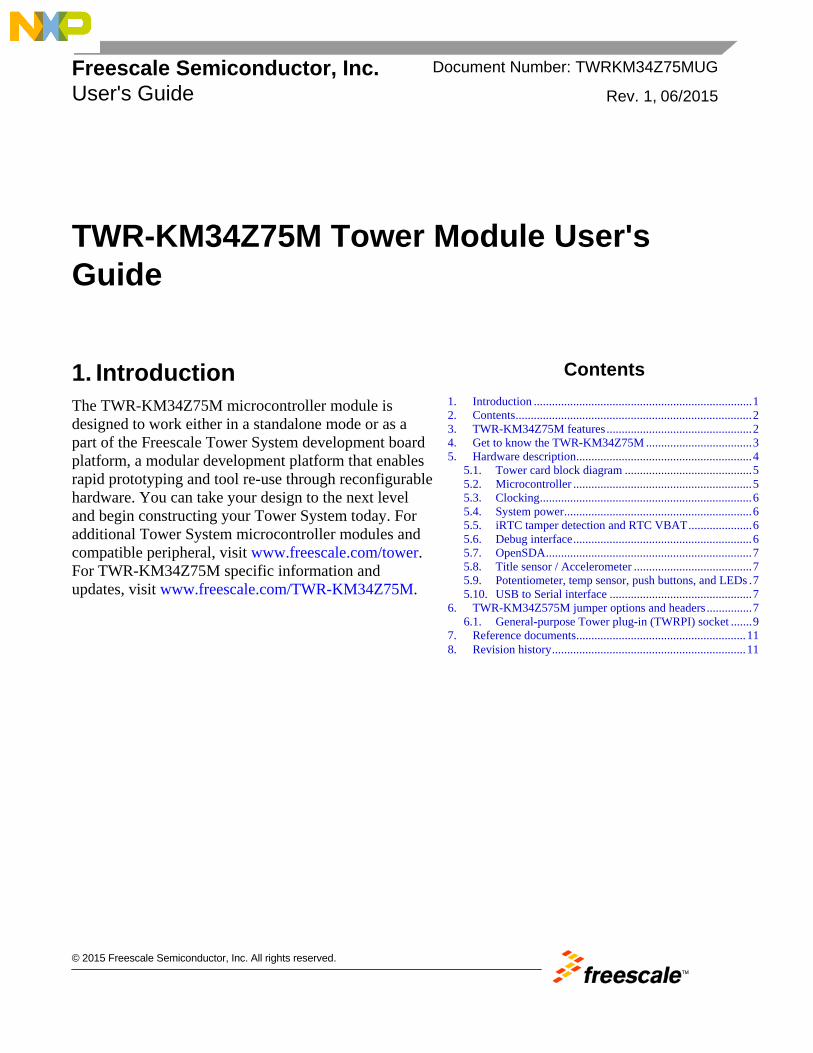
TWR-KM34Z75M Tower Module User's Guide
1. Introduction The TWR-KM34Z75M microcontroller module is designed to work either in a standalone mode or as a part of the Freescale Tower System development board platform, a modular development platform that enables rapid prototyping and tool re-use through reconfigurable hardware. You can take your design to the next level and begin constructing your Tower System today. For additional Tower System microcontroller modules and compatible peripheral, visit www.freescale.com/tower. For TWR-KM34Z75M specific information and updates, visit www.freescale.com/TWR-KM34Z75M.
Freescale Semiconductor, Inc. Document Number: TWRKM34Z75MUG
User's Guide Rev. 1 , 06/2015
Contents 1. Introduction ........................................................................ 1 2. Contents .............................................................................. 2 3. TWR-KM34Z75M features ................................................ 2 4. Get to know the TWR-KM34Z75M ................................... 3 5. Hardware description .......................................................... 4
5.1. Tower card block diagram .......................................... 5 5.2. Microcontroller ........................................................... 5 5.3. Clocking ...................................................................... 6 5.4. System power .............................................................. 6 5.5. iRTC tamper detection and RTC VBAT ..................... 6 5.6. Debug interface ........................................................... 6 5.7. OpenSDA .................................................................... 7 5.8. Title sensor / Accelerometer ....................................... 7 5.9. Potentiometer, temp sensor, push buttons, and LEDs . 7 5.10. USB to Serial interface ............................................... 7
6. TWR-KM34Z575M jumper options and headers ............... 7 6.1. General-purpose Tower plug-in (TWRPI) socket ....... 9
7. Reference documents ........................................................ 11 8. Revision history ................................................................ 11
© 2015 Freescale Semiconductor, Inc. All rights reserved.
TWR-KM34Z75M features
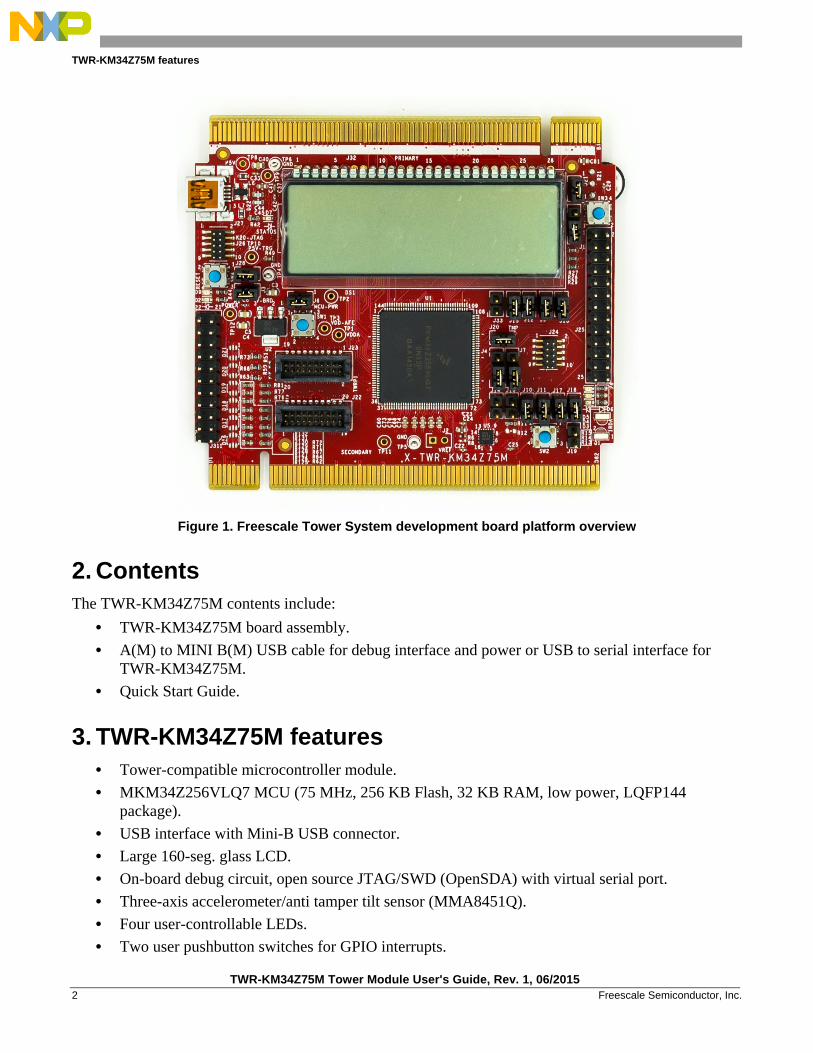
Figure 1. Freescale Tower System development board platform overview
2. Contents The TWR-KM34Z75M contents include:
• TWR-KM34Z75M board assembly. • A(M) to MINI B(M) USB cable for debug interface and power or USB to serial interface for
TWR-KM34Z75M. • Quick Start Guide.
3. TWR-KM34Z75M features • Tower-compatible microcontroller module. • MKM34Z256VLQ7 MCU (75 MHz, 256 KB Flash, 32 KB RAM, low power, LQFP144
package). • USB interface with Mini-B USB connector. • Large 160-seg. glass LCD. • On-board debug circuit, open source JTAG/SWD (OpenSDA) with virtual serial port. • Three-axis accelerometer/anti tamper tilt sensor (MMA8451Q). • Four user-controllable LEDs. • Two user pushbutton switches for GPIO interrupts.
TWR-KM34Z75M Tower Module User's Guide, Rev. 1, 06/2015 2 Freescale Semiconductor, Inc.
Get to know the TWR-KM34Z75M
• One user pushbutton switch for tamper detection. • One user pushbutton switch for MCU reset. • Potentiometer. • Headers for direct GPIO and ADC access. • External Tamper pins. • Independent, battery-operated power supply for Real Time Clock (RTC) and tamper detection
modules. • IRDA support. • NTC temperature sensor. • General-purpose Tower Plug-in (TWRPI) socket.
4. Get to know the TWR-KM34Z75M
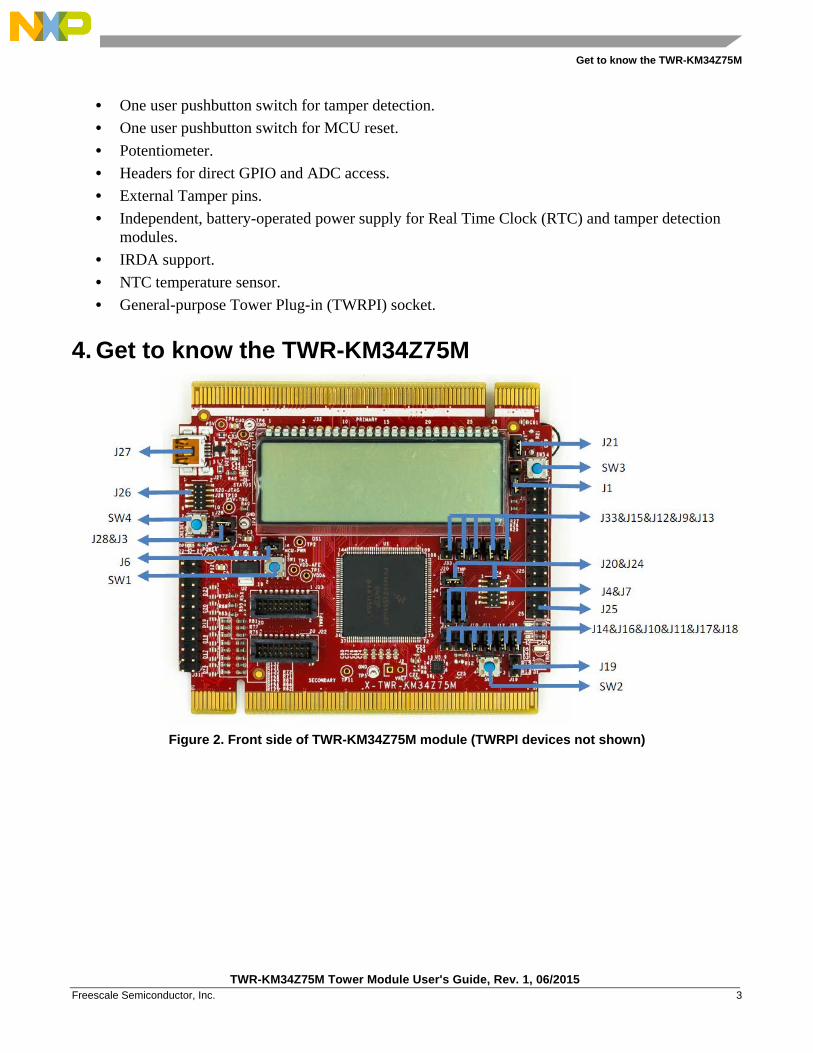
Figure 2. Front side of TWR-KM34Z75M module (TWRPI devices not shown)
TWR-KM34Z75M Tower Module User's Guide, Rev. 1, 06/2015 Freescale Semiconductor, Inc. 3
Hardware description
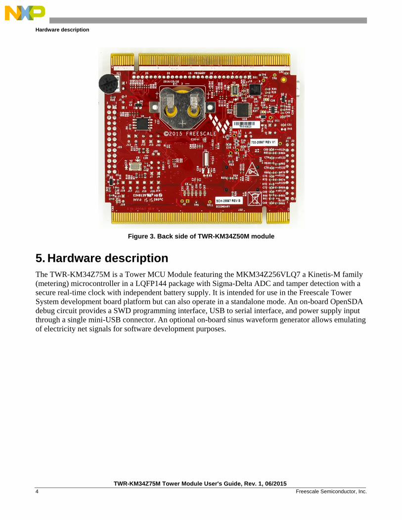
Figure 3. Back side of TWR-KM34Z50M module
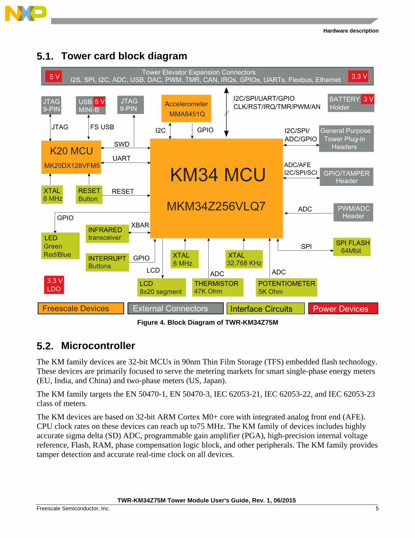
5. Hardware description The TWR-KM34Z75M is a Tower MCU Module featuring the MKM34Z256VLQ7 a Kinetis-M family (metering) microcontroller in a LQFP144 package with Sigma-Delta ADC and tamper detection with a secure real-time clock with independent battery supply. It is intended for use in the Freescale Tower System development board platform but can also operate in a standalone mode. An on-board OpenSDA debug circuit provides a SWD programming interface, USB to serial interface, and power supply input through a single mini-USB connector. An optional on-board sinus waveform generator allows emulating of electricity net signals for software development purposes.
TWR-KM34Z75M Tower Module User's Guide, Rev. 1, 06/2015 4 Freescale Semiconductor, Inc.
Hardware description
5.1. Tower card block diagram
Figure 4. Block Diagram of TWR-KM34Z75M
5.2. Microcontroller The KM family devices are 32-bit MCUs in 90nm Thin Film Storage (TFS) embedded flash technology. These devices are primarily focused to serve the metering markets for smart single-phase energy meters (EU, India, and China) and two-phase meters (US, Japan).
The KM family targets the EN 50470-1, EN 50470-3, IEC 62053-21, IEC 62053-22, and IEC 62053-23 class of meters.
The KM devices are based on 32-bit ARM Cortex M0+ core with integrated analog front end (AFE). CPU clock rates on these devices can reach up to75 MHz. The KM family of devices includes highly accurate sigma delta (SD) ADC, programmable gain amplifier (PGA), high-precision internal voltage reference, Flash, RAM, phase compensation logic block, and other peripherals. The KM family provides tamper detection and accurate real-time clock on all devices.
MK20DX128VFM5
K20 MCU
AccelerometerMMA8451Q
INTERRUPTButtons
RESETButton
JTAG9-PIN
JTAG9-PIN
PWM/ADCHeader
General Purpose Tower Plug-in
Headers
LCD8x20 segment
POTENTIOMETER5K Ohm
XTAL8 MHz
THERMISTOR47K Ohm
Tower Elevator Expansion ConnectorsI2S, SPI, I2C, ADC, USB, DAC, PWM, TMR, CAN, IRQs, GPIOs, UARTs, Flexbus, Ethernet5 V 3.3 V
USBMINI-B
5 V
3.3 V LDO
GPIO/TAMPER Header
Freescale Devices External Connectors Interface Circuits Power Devices
XTAL8 MHz
GPIO
UART
SWD
FS USB
ADC
LCD ADC
JTAG
I2C/SPI/UART/GPIOCLK/RST/IRQ/TMR/PWM/AN
GPIO
RESET
LEDGreenRed/Blue
I2C/SPI/ADC/GPIO
XTAL32.768 KHz
ADC
BATTERYHolder
3 V
MKM34Z256VLQ7
KM34 MCU
SPI FLASH64Mbit
INFRAREDtransceiver
XBAR
I2C GPIO
ADC/AFEI2C/SPI/SCI
SPI
TWR-KM34Z75M Tower Module User's Guide, Rev. 1, 06/2015 Freescale Semiconductor, Inc. 5
Hardware description
5.3. Clocking The Kinetis-M start up from an internal reference clock = 2MHz core and 1MHz bus clock. The microcontroller can boot in LPBOOT (Low Power Boot) mode, core, and system clk. is then divided by eight.
The CPU software can enable the RTC oscillator connected to (EXTAL0/XTAL0) if desired, or use the second high frequency oscillator connected to (EXTAL1/XTAL1).
The RTC crystal oscillator range is: 31.25 kHz to 39.0625 kHz (typ. 32.768 kHz).
The high frequency crystal oscillator range: 1 to 32 MHz.
Optionally, you can also use two internal clock references (IRC): fast = 4MHz and slow = 32.768 kHz.
You can increase the CPU frequency by using the FLL (DCO) or PLL clock features. In most of the applications, usage of the single 32 kHz external crystal is considered. PLL with a fixed multiplier = x375 is used for clocking the AFE running at ~12.2 MHz. The FLL is used for clocking the CPU core (up to 75 MHz) and the rest of the microcontroller modules.
NOTE For the best AFE results, usage of the precise external clock is recommended.
5.4. System power When installed into a Tower System, you can power the TWR-KM34Z75M from either an on-board source or from another source in the assembled Tower System.
In a stand-alone operation, the main power source (5.0 V) for the TWR-KM34Z75M module is derived from either the OpenSDA USB mini-B connector (J14). A low-dropout regulator provides 3.3 V supply voltage from the 5.0 V input voltage.
5.5. iRTC tamper detection and RTC VBAT The tamper detection module and the Real Time Clock (RTC) module on the MKM34Z256VLQ7 have two modes of operation: system power-up and system power-down. During system power-down, the tamper detection module and the RTC are powered from the backup power supply (VBAT) and electrically isolated from the rest of the microcontroller. The TWR-KM34Z75M provides a battery receptacle for a coin cell battery that is used as the VBAT supply. The receptacle can accept common 20-mm diameter 3 V lithium coin cell batteries.
5.6. Debug interface There are two debug interface options provided: the on-board OpenSDA circuit and an external ARM JTAG/SWD connector. The ARM-JTAG/SWD connector is a standard 2x5-pin connector providing an external debugger cable with access to the JTAG interface of the MKM34Z256VLQ7. Alternatively, the on-board OSJTAG debug interface is used to access the debug interface of the MKM34Z256VLQ7.
TWR-KM34Z75M Tower Module User's Guide, Rev. 1, 06/2015 6 Freescale Semiconductor, Inc.
TWR-KM34Z575M jumper options and headers
5.7. OpenSDA An on-board MK20DX128VMF5 based OpenSDA circuit provides a SWD debug interface to the MKM34Z256VLQ7. A standard USB A male to mini-B male cable (provided) is used for debugging via the USB connector (J14). The OpenSDA interface also provides a USB to serial bridge. Drivers for the OpenSDA interface are provided in the P&E Micro OSBDM/OSJTAG Tower Toolkit. These drivers and more utilities can be found online at http://www.pemicro.com/opensda.
5.8. Title sensor / Accelerometer MMA8451Q digital accelerometer is connected to the MKM34Z256VLQ7 MCU through an I2C interface (I2C0) and GPIO signals.
5.9. Potentiometer, temp sensor, push buttons, and LEDs The TWR-KM34Z75M also features:
• A potentiometer connected to an ADC input signal (PTF1/ADC0_SE8). • Temperature sensor (NTC) connected to an ADC input signal (PTF2/ADC0_SE9). • Two pushbutton switches (SW1 and SW2 connected to PTA4 and PTD1, respectively). • IRDA interface through PTL2, PTD0. • Three user-controllable LEDs connected to GPIO signals:
— Green LED (D3) to PTJ3. — Red LED (D4) to PTJ4. — Orange LED (D5) to PTD0.
5.10. USB to Serial interface The on-board K20 OpenSDA circuit supports the USB to Serial port emulation through the USB CDC Serial Class device.
This means whenever the Tower card is connected to the computer USB port, the board is recognized as a new virtual COM port (COM5 or COM6 in the most of the cases). You can connect the embedded application running on KM34 device and see the output on the PC running the serial terminal application.
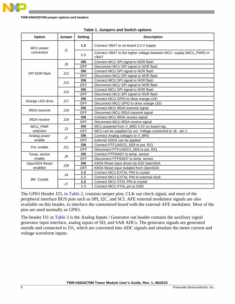
6. TWR-KM34Z575M jumper options and headers The following is a list of all the jumper options on the TWR-KM34Z75M, the default installed jumper settings are indicated in Table 1 by BOLD text.
TWR-KM34Z75M Tower Module User's Guide, Rev. 1, 06/2015 Freescale Semiconductor, Inc. 7
TWR-KM34Z575M jumper options and headers
Table 1. Jumpers and Switch options
Option Jumper Setting Description
MCU power connection J1
1-2 Connect VBAT to on-board 3.3 V supply
2-3 Connect VBAT to the higher voltage between MCU supply (MCU_PWR) or VBAT
SPI NOR flash
J9 ON Connect MCU SPI signal to NOR flash OFF Disconnect MCU SPI signal to NOR flash
J12 ON Connect MCU SPI signal to NOR flash OFF Disconnect MCU SPI signal to NOR flash
J13 ON Connect MCU SPI signal to NOR flash OFF Disconnect MCU SPI signal to NOR flash
J15 ON Connect MCU SPI signal to NOR flash OFF Disconnect MCU SPI signal to NOR flash
Orange LED drive J17 ON Connect MCU GPIO to drive orange LED OFF Disconnect MCU GPIO to drive orange LED
IRDA transmit J18 ON Connect MCU IRDA transmit signal OFF Disconnect MCU IRDA transmit signal
IRDA receive J19 ON Connect MCU IRDA receive signal OFF Disconnect MCU IRDA receive signal
MCU_PWR selection J3
ON MCU powered from V_BRD 3.3V on board reg. OFF MCU can be supplied by ext. Voltage connected to J6 - pin 1
Analog power enable J7
ON Connect Analog voltages to V_BRD OFF external VDDA can be applied
Pot. enable J21 ON Connect PTF1/ADC0_SE8 to pot. R21 OFF Disconnect PTF1/ADC0_SE8 to pot. R21
Temp. sensor enable J9
ON Connect PTF0/AD7 to temp. sensor OFF Disconnect PTF0/AD7 to temp. sensor
OpenSDA Reset enabled J28
ON KM34 Reset input driven by K20 OpenSDA OFF KM34 Reset input isolated from OpenSDA
8M Crystal J4
1-2 Connect MCU EXTAL PIN to crystal 2-3 Connect MCU EXTAL PIN to external clock
J7 1-2 Connect MCU XTAL PIN to crystal 2-3 Connect MCU XTAL pin to GND
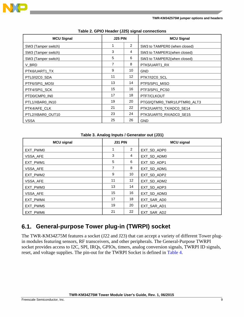
The GPIO Header J25, in Table 2, contains tamper pins, CLK out check signal, and most of the peripheral interface BUS pins such as SPI, I2C, and SCI. AFE external modulator signals are also available on this header, to interface the customized board with the external AFE modulator. Most of the pins are used normally as GPIO.
The header J31 in Table 3 is the Analog Inputs / Generator out header contains the auxiliary signal generator input interface, analog inputs of SD, and SAR ADCs. The generator signals are generated outside and connected to J31, which are converted into ADC signals and simulate the meter current and voltage waveform inputs.
TWR-KM34Z75M Tower Module User's Guide, Rev. 1, 06/2015 8 Freescale Semiconductor, Inc.
TWR-KM34Z575M jumper options and headers
Table 2. GPIO Header (J25) signal connections
MCU Signal J25 PIN MCU Signal
SW3 (Tamper switch) 1 2 SW3 to TAMPER0 (when closed)
SW3 (Tamper switch) 3 4 SW3 to TAMPER1(when closed)
SW3 (Tamper switch) 5 6 SW3 to TAMPER2(when closed)
V_BRD 7 8 PTK5/UART1_RX
PTK6/UART1_TX 9 10 GND
PTL0/I2C0_SDA 11 12 PTK7/I2C0_SCL
PTF6/SPI1_MOSI 13 14 PTF5/SPI1_MISO
PTF4/SPI1_SCK 15 16 PTF3/SPI1_PCS0
PTD0/CMP0_IN0 17 18 PTF7/CLKOUT
PTL1/XBAR0_IN10 19 20 PTG0/QTMR0_TMR1/LPTMR0_ALT3
PTK4/AFE_CLK 21 22 PTK2/UART0_TX/ADC0_SE14
PTL2/XBAR0_OUT10 23 24 PTK3/UART0_RX/ADC0_SE15
VSSA 25 26 GND
Table 3. Analog Inputs / Generator out (J31)
MCU signal J31 PIN MCU signal
EXT_PWM0 1 2 EXT_SD_ADP0
VSSA_AFE 3 4 EXT_SD_ADM0
EXT_PWM1 5 6 EXT_SD_ADP1
VSSA_AFE 7 8 EXT_SD_ADM1
EXT_PWM2 9 10 EXT_SD_ADP2
VSSA_AFE 11 12 EXT_SD_ADM2
EXT_PWM3 13 14 EXT_SD_ADP3
VSSA_AFE 15 16 EXT_SD_ADM3
EXT_PWM4 17 18 EXT_SAR_AD0
EXT_PWM5 19 20 EXT_SAR_AD1
EXT_PWM6 21 22 EXT_SAR_AD2
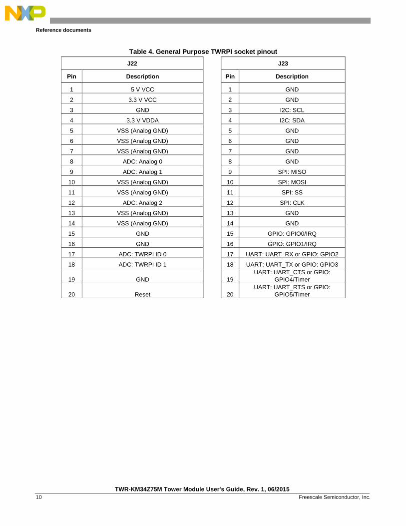
6.1. General-purpose Tower plug-in (TWRPI) socket The TWR-KM34Z75M features a socket (J22 and J23) that can accept a variety of different Tower plug-in modules featuring sensors, RF transceivers, and other peripherals. The General-Purpose TWRPI socket provides access to I2C, SPI, IRQs, GPIOs, timers, analog conversion signals, TWRPI ID signals, reset, and voltage supplies. The pin-out for the TWRPI Socket is defined in Table 4.
TWR-KM34Z75M Tower Module User's Guide, Rev. 1, 06/2015 Freescale Semiconductor, Inc. 9
Reference documents
Table 4. General Purpose TWRPI socket pinout
J22
J23
Pin Description
Pin Description
1 5 V VCC
1 GND
2 3.3 V VCC
2 GND
3 GND
3 I2C: SCL
4 3.3 V VDDA
4 I2C: SDA
5 VSS (Analog GND)
5 GND
6 VSS (Analog GND)
6 GND
7 VSS (Analog GND)
7 GND
8 ADC: Analog 0
8 GND
9 ADC: Analog 1
9 SPI: MISO
10 VSS (Analog GND)
10 SPI: MOSI
11 VSS (Analog GND)
11 SPI: SS
12 ADC: Analog 2
12 SPI: CLK
13 VSS (Analog GND)
13 GND
14 VSS (Analog GND)
14 GND
15 GND
15 GPIO: GPIO0/IRQ
16 GND
16 GPIO: GPIO1/IRQ
17 ADC: TWRPI ID 0
17 UART: UART_RX or GPIO: GPIO2
18 ADC: TWRPI ID 1
18 UART: UART_TX or GPIO: GPIO3
19 GND
19 UART: UART_CTS or GPIO:
GPIO4/Timer
20 Reset
20 UART: UART_RTS or GPIO:
GPIO5/Timer
TWR-KM34Z75M Tower Module User's Guide, Rev. 1, 06/2015 10 Freescale Semiconductor, Inc.
Revision history
7. Reference documents For more information on the Kinetis family, Tower System, and MCU Modules, see the following documents. These can be found in the documentation section of http://www.freescale.com/TWR-KM34Z75M or http://www.freescale.com/kinetis.
• TWR-KM34Z75M-SCH: Schematics (document TWR-KM34Z75M-SCH) • TWR-KM34Z75M-PWB: Design Package (document TWR-KM34Z75M-PWB) • KM34P144M75SF0RM: Reference Manual (document KM34P144M75SF0RM) • Tower Configuration Tool (document TOWER_CONFIG_TOOL) • Tower Mechanical Drawing (document 900-76126_TWR-MECHDRW)
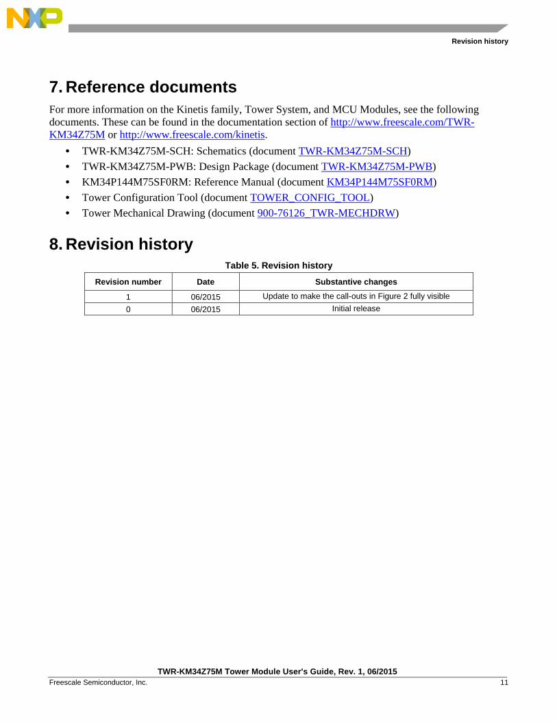
8. Revision history Table 5. Revision history
Revision number Date Substantive changes
1 06/2015 Update to make the call-outs in Figure 2 fully visible 0 06/2015 Initial release
TWR-KM34Z75M Tower Module User's Guide, Rev. 1, 06/2015 Freescale Semiconductor, Inc. 11
How to Reach Us:
Home Page: freescale.com
Web Support: freescale.com/support
Information in this document is provided solely to enable system and software implementers to use Freescale products. There are no express or implied copyright licenses granted hereunder to design or fabricate any integrated circuits based on the information in this document.
Freescale reserves the right to make changes without further notice to any products herein. Freescale makes no warranty, representation, or guarantee regarding the suitability of its products for any particular purpose, nor does Freescale assume any liability arising out of the application or use of any product or circuit, and specifically disclaims any and all liability, including without limitation consequential or incidental damages. “Typical” parameters that may be provided in Freescale data sheets and/or specifications can and do vary in different applications, and actual performance may vary over time. All operating parameters, including “typicals,” must be validated for each customer application by customer's technical experts. Freescale does not convey any license under its patent rights nor the rights of others. Freescale sells products pursuant to standard terms and conditions of sale, which can be found at the following address: freescale.com/SalesTermsandConditions.
Freescale, the Freescale logo and Kinetis are trademarks of Freescale Semiconductor, Inc., Reg. U.S. Pat. & Tm. Off. All other product or service names are the property of their respective owners. ARM, ARM Powered and Cortex are registered trademarks of ARM Limited (or its subsidiaries) in the EU and/or elsewhere. All rights reserved.
© 2015 Freescale Semiconductor, Inc.
Document Number: TWRKM34Z75MUG Rev. 1
06/2015