Embed Size (px)
Citation preview

ADCxxQJxx00 Evaluation Module
User's Guide
Literature Number: SLAU808February 2020

2 SLAU808–February 2020Submit Documentation Feedback
Copyright © 2020, Texas Instruments Incorporated
Contents
Contents
Preface ........................................................................................................................................ 41 Introduction......................................................................................................................... 52 Equipment........................................................................................................................... 7
2.1 Evaluation Board Feature Identification Summary ...................................................................... 72.2 Required Equipment......................................................................................................... 8
3 Setup Procedure .................................................................................................................. 93.1 Install the High Speed Data Converter (HSDC) Pro Software ......................................................... 93.2 Install the Configuration GUI Software.................................................................................... 93.3 Connect the ADCxxQxx00EVM and TSW14J57EVM ................................................................. 103.4 Connect the Power Supplies to the Boards (Power Off) .............................................................. 103.5 Connect the Signal Generators to the EVM (RF Outputs Disabled Until Directed) ............................... 103.6 Turn On the TSW14J57EVM Power and Connect to the PC ........................................................ 113.7 Turn On the ADCxxQJxx00EVM Power Supplies and Connect to the PC ......................................... 113.8 Turn On the Signal Generator RF Outputs ............................................................................. 113.9 Open the ADCxxQJxx00EVM GUI and Program the ADC and Clocks ............................................. 113.10 Calibrate the ADC Device on the EVM .................................................................................. 123.11 Open the HSDCpro Software and Load the FPGA Image to the TSW14J57EVM ................................ 133.12 Capture Data Using the HSDC Pro Software .......................................................................... 14
4 Device Configuration .......................................................................................................... 164.1 Supported JESD204C Device Features................................................................................. 164.2 Tab Organization ........................................................................................................... 164.3 Low-Level Control .......................................................................................................... 17
5 Troubleshooting the ADCxxQJxx00EVM ............................................................................... 18A References ........................................................................................................................ 19
A.1 Technical Reference Documents......................................................................................... 19A.2 TSW14J57EVM Operation ................................................................................................ 19
B HSDC Pro Settings for Optional ADC Device Configuration ..................................................... 20B.1 Changing the Number of Frames per Multi-Frame (K) ................................................................ 20B.2 Customizing the EVM for Optional Clocking Support ................................................................. 20
B.2.1 "Ext CLK from LMK to ADC" (Default).......................................................................... 21B.2.2 "Ext Direct CLK to ADC Clocking Option" ..................................................................... 22B.2.3 "Onboard 50M Ref to ADC PLL" ................................................................................ 23B.2.4 "Ext Ref to ADC PLL" ............................................................................................ 24
C Signal Routing .................................................................................................................. 27C.1 Signal Routing .............................................................................................................. 27
D Analog Inputs .................................................................................................................... 28E Jumpers and LEDs ............................................................................................................ 29
E.1 Jumper settings............................................................................................................. 29

www.ti.com
3SLAU808–February 2020Submit Documentation Feedback
Copyright © 2020, Texas Instruments Incorporated
List of Figures
List of Figures1-1. EVM Orientation ............................................................................................................. 62-1. EVM Feature Locations ..................................................................................................... 73-1. EVM Test Setup.............................................................................................................. 93-2. Configuration GUI EVM Tab .............................................................................................. 113-3. Configuration GUI ADC Control .......................................................................................... 123-4. High Speed Data Converter Pro (HSDC) GUI.......................................................................... 143-5. SYSREF Coupling.......................................................................................................... 153-6. SYSREF Pulses ............................................................................................................ 154-1. Low-Level Register Control Tab ......................................................................................... 17B-1. ADCxxQJxx00EVM Clocking System Block Diagram ................................................................. 21B-2. Ext Direct CLK to ADC System Block Diagram ........................................................................ 22B-3. Onboard 50M Ref to ADC PLL System Block Diagram ............................................................... 23B-4. Ext Ref to ADC PLL System Block Diagram ........................................................................... 24B-5. Ext CLK from LMK to ADC Configuration ............................................................................... 25B-6. Ext Direct clock to ADC Configuration................................................................................... 26D-1. Analog Input Path .......................................................................................................... 28
List of Tables4-1. Supported and Non-Supported Features of the JESD204C Device................................................. 164-2. Low-Level Controls......................................................................................................... 175-1. Troubleshooting ............................................................................................................ 18C-1. ADCxxQJxx00EVM Signal Routing ..................................................................................... 27D-1. Analog Input Path .......................................................................................................... 28E-1. Jumper Settings ............................................................................................................ 29E-2. LEDs ......................................................................................................................... 29
4 SLAU808–February 2020Submit Documentation Feedback
Copyright © 2020, Texas Instruments Incorporated
PrefaceSLAU808–February 2020
This user’s guide describes the characteristics, operation, and use of the ADCxxQJxx00 evaluationmodule (EVM). This user's guide discusses how to set up and configure the software and hardware, andreviews various aspects of the program operation. Throughout this document, the terms evaluation board,evaluation module, and EVM are synonymous with the ADCxxQJxx00EVM. In the following sections ofthis document, the ADCxxQJxx00 evaluation board is referred to as the EVM and the ADCxxQJxx00device is referred to as the ADC device. This document also includes an electrical schematic, printedcircuit board (PCB) layout drawings, and a parts list for the EVM.
TrademarksK&L Microwave is a trademark of K&L Microwave.Microsoft, Windows are registered trademarks of Microsoft Corporation.Rohde & Schwarz is a registered trademark of Rohde & Schwarz GmbH & Co.Trilithic is a trademark of Trilithic, Inc.All other trademarks are the property of their respective owners.

5SLAU808–February 2020Submit Documentation Feedback
Copyright © 2020, Texas Instruments Incorporated
Introduction
Chapter 1SLAU808–February 2020
Introduction
The ADCxxQJxx00EVM is an evaluation board used to evaluate the ADCxxQJxx00 family (ADC09QJ1300and ADC12QJ1600) of analog-to-digital converters (ADC) from Texas Instruments. The ADCxxQJxx00 isa quad channel, 9 or 12-bit ADC, capable of operating at sampling rates up to 1.6 Giga-samples persecond (GSPS) with four analog input channels. The ADCxxQJxx00EVM output data is transmitted over astandard JESD204C high-speed serial interface. This evaluation board also includes the followingimportant features:• Transformer-coupled signal input network allowing a single-ended signal source from 10 MHz to
4 GHz. Option to bypass the transformer and use DC coupled differential inputs• The LMK04828 onboard system clock generator generates ADC sampling clock, SYSREF and FPGA
reference clocks for the high-speed serial interface• Transformer-coupled clock input network to test the ADC performance with an external low-noise clock
source• LM95233 temperature sensor• High-speed serial data output over a High Pin Count FMC interface connector
NOTE: To improve signal routing quality, serial lanes are mapped differently with respect to thestandard FMC VITA-57 signal mapping. Signal mapping is shown in Table C-1).
• Device register programming through USB connector and FTDI USB-to-SPI bus translator

Copyright © 2018, Texas Instruments Incorporated
IND( J8 )
ADC12QJ1600
ADC12QJ1600 EVM top side
INA
( J3 )
USB
Connector+12V DC
ADC12QJ1600 EVM top side
Power (DC/DC
and LDO¶s)
LMK CLKJ31
INC+/-INB+/-
EXT CLK
( J10 )
FMC
connector
LMK04828
50 MHz
Crystal Osc
ADC12DJ1600 EVM bottom side
LM95233
Copyright © 2016, Texas Instruments Incorporated
INB( J7 )
INC
( J4 )
INA+/- IND+/-
www.ti.com
6 SLAU808–February 2020Submit Documentation Feedback
Copyright © 2020, Texas Instruments Incorporated
Introduction
Figure 1-1. EVM Orientation
The digital data from the ADCxxQJxx00EVM board is quickly and easily captured with the TSW14J57EVMdata capture boards.
NOTE: The TSW14J57EVM cannot be used for JMODES (4 to 8, 14 and 15 ) that use 64b/66bencoding, or SERDES lane rate above 15 Gbps.
The TSW14J57EVM captures the high-speed serial data, decodes the data, stores the data in memory,and then uploads it to a connected PC through a USB interface for analysis. The High-Speed DataConverter Pro (HSDC Pro) software on the PC communicates with the hardware and processes the data.
With proper hardware selection in the HSDCpro software, the TSW14J57 device is automaticallyconfigured to support a wide range of operating speeds of the ADCxxQJxx00EVM, but the device may notcover the full operating range of the ADC device. Serial data rates of 15 Gbps down to 1 Gbps aresupported.

INC+/-INB+/-
EXT CLK
( J10 )
INA+/- IND+/-
LMK CLK
(J31)
Jumpers
Over-range
LEDs
High Temp
LED
USB LED
Mini USB Connector
(J20)12V DC
(J14)
Board power
LED
Copyright © 2018, Texas Instruments Incorporated
7SLAU808–February 2020Submit Documentation Feedback
Copyright © 2020, Texas Instruments Incorporated
Equipment
Chapter 2SLAU808–February 2020
Equipment
This section describes how to setup the EVM on the bench with the proper equipment to evaluate the fullperformance of the ADC device.
2.1 Evaluation Board Feature Identification Summary
Figure 2-1. EVM Feature Locations

Required Equipment www.ti.com
8 SLAU808–February 2020Submit Documentation Feedback
Copyright © 2020, Texas Instruments Incorporated
Equipment
2.2 Required EquipmentThe following equipment and documents are included in the EVM evaluation kit:• Evaluation board (EVM)• Mini-USB cable• Power cable
The following equipment is not included in the EVM evaluation kit, but is required for evaluation of thisproduct:• TSW14J57EVM data capture board and related items• PC computer running Microsoft® Windows® 7, or 10• One low-noise signal generator for DEVCLK (Sampling clock) . TI recommends the following
generators:– Rohde & Schwarz® SMA100B– Rohde & Schwarz® SMA100A
• One low-noise signal generator for analog input. TI recommends the following generators:– Rohde & Schwarz® SMA100B– Rohde & Schwarz® SMA100A
• Bandpass filter for analog input signal (97 MHz or desired frequency). The following filters arerecommended:– Bandpass filter, greater than or equal to 60-dB harmonic attenuation, less than or equal to 5%
bandwidth, greater than 18-dBm power, less than 5-dB insertion loss– Trilithic™ 5VH-series tunable BPF– K&L Microwave™ BT-series tunable BPF– TTE KC6 or KC7-series fixed BPF
• Signal-path cables, SMA or BNC (or both SMA and BNC)
By default, the ADCxxQJxx00EVM is configured to use LMK04828 in distribution mode to provide thesampling clock to the ADC (In the GUI this option is labeled as "Ext CLK from LMK to ADC"). A few smallboard modifications allow the direct external sampling clock option(In the GUI this option is labeled as "ExtDirect CLK to ADC"). If direct external clocking option is used, the following additional equipment isrecommended.• Signal generators for providing the FPGA reference clock . TI recommends similar models to the
DEVCLK clock source.
NOTE: The frequency of clock source used to drive the FPGA reference clock (labeled DEV CLKJ31) is displayed on the first page of the GUI under FPGA Reference Clock. The FPGAreference clock frequency is calculated by the GUI using JMODE and the samplingfrequency (Fs) entered by the user. If "Ext Direct CLK to ADC" the FPGA reference clockgenerator and device clock generator must be frequency-locked using a common 10-MHzreference.

PC Running
ADC GUI
12-V DC
Power Supply
PC Running
HSDCpro
12-V DC
Power Supply
1600MHz Sampling Clock
Signal Gen.
97MHz Input
Signal Gen.
Bandpass Filter
Bandpass Filter
Frequency Locked
using 10 MHz
Reference
Copyright © 2016, Texas Instruments Incorporated
9SLAU808–February 2020Submit Documentation Feedback
Copyright © 2020, Texas Instruments Incorporated
Setup Procedure
Chapter 3SLAU808–February 2020
Setup Procedure
Figure 3-1. EVM Test Setup
NOTE: The HSDC Pro software must be installed before connecting the TSW14J57EVM to the PCfor the first time.
3.1 Install the High Speed Data Converter (HSDC) Pro Software1. Download the most recent version of the HSDC Pro software from www.ti.com/tool/dataconverterpro-
sw. Follow the installation instructions to install the software.2. Download and copy all the INI files required to the HSDCpro directory from ADC12QJ1600EVM
webpage. The INI files should be copied to following location C:\Program Files (x86)\TexasInstruments\High Speed Data Converter Pro\14J57revE Details\ADC files
3.2 Install the Configuration GUI Software1. Download the ADC12QJ1600EVM configuration GUI software from ADC12QJ1600EVM webpage.2. Extract files from the .zip file.3. Run the executable file (setup.exe), and follow the instructions. Make sure to install and run the
software as an administrator.

Connect the ADCxxQxx00EVM and TSW14J57EVM www.ti.com
10 SLAU808–February 2020Submit Documentation Feedback
Copyright © 2020, Texas Instruments Incorporated
Setup Procedure
3.3 Connect the ADCxxQxx00EVM and TSW14J57EVMWith the power off, connect the ADCxxQJxx00EVM to the TSW14J57EVM through the FMC connector asshown in Figure 3-1. Ensure that the standoffs provide the proper height for robust connector connections.
3.4 Connect the Power Supplies to the Boards (Power Off)1. Confirm that the power switch on the TSW14J57EVM is in the off position. Connect the power cable to
a 12-V DC (minimum 3 A) power supply. Ensure the proper supply polarity by confirming that the outersurface of the barrel connector is GND and the inner portion of the connector is 12 V. Connect thepower cable to the EVM power connector.
2. Confirm that the power switch for the ADCxxQJxx00EVM's power supply is in the off position. Connectthe power cable to a 12-V DC (minimum 1.5 A) power supply. Ensure the proper supply polarity byconfirming that the outer surface of the barrel connector is GND and the inner portion of the connectoris 12 V. Connect the power cable to the EVM power connector.
CAUTIONEnsure the power connections to the EVMs are the correct polarity.Failure to do so may result in immediate damage.Leave the power switches in the off position until directed later.
3.5 Connect the Signal Generators to the EVM (RF Outputs Disabled Until Directed)Connect a signal generator to the INAP (J3) input of the ADCxxQJxx00EVM through a bandpass filter andat the SMA connector. This must be a low-noise signal generator. TI recommends a Trilithic-tunablebandpass filter to filter the signal from the generator. Configure the signal generator for 97 MHz, 6 dBm.
When LMK04828 is used for clocking the ADC(Default)a. Connect a signal generator to the LMK CLK (J31) input of the EVM through a bandpass filter. This
signal generator must be a low-noise signal generator. TI recommends a Trilithic-tunable bandpassfilter to filter the signal coming from the generator. Configure the signal generator for the desired clockfrequency in the range of 0.5 to 1.6 GHz. For best performance when using an RF signal generator,the power input to the LMK CLK SMA connector must be 5 dBm (1.125 Vpp into 50 Ω). The signalgenerator must increase above 5 dB by an amount equal to any additional attenuation in the clocksignal path, such as the insertion loss of the bandpass filter. For example, if the filter insertion loss is 2dB, the signal generator must be set to 5 dBm + 2 dB = 7 dBm.
b. Skip this step for default("Ext CLK from LMK to ADC") evm setup. This step should only be followedwhen Ext Direct CLK to ADC mode is desired. The ADC sampling clock of desired frequency(1600MHz) is applied to the SMA connector EXT CLK(J10) and the FPGA reference signal input for the EVMat is applied at LMC CLK(J31). Configure the signal generator for the FPGA reference desired(320MHz) clock frequency. Set the output power to approximately 6–9 dBm.
NOTE:1. The FPGA Reference clock frequency can be obtained from the ADCxxQJxx00EVM
GUI. Once the ADCxxQJxx00EVM GUI is configured to the desired JMODE mode andclock rate. The Reference Clock frequency required by the EVM is displayed on firstpage of the GUI shown with red square in Figure 3-2
2. Ensure that the DEVCLK and FPGA Reference clock sources are frequency-lockedusing a common 10-MHz reference to ensure functionality. Frequency locking the inputsignal generator to the other generators can also be done if coherent sampling isdesired.
3. Do not turn on the RF output of any signal generator at this time.

Copyright © 2018, Texas Instruments Incorporated
www.ti.com Turn On the TSW14J57EVM Power and Connect to the PC
11SLAU808–February 2020Submit Documentation Feedback
Copyright © 2020, Texas Instruments Incorporated
Setup Procedure
3.6 Turn On the TSW14J57EVM Power and Connect to the PC1. Turn on the power switch of the TSW14J57EVM.2. Connect the USB cable from the PC to the TSW14J57EVM.3. If this is the first time connecting the TSW14J57EVM to the PC, follow the on-screen instructions to
automatically install the device drivers. See the TSW14J57EVM user's guide for specific instructions.
3.7 Turn On the ADCxxQJxx00EVM Power Supplies and Connect to the PC1. Turn on the 12-V power supply to power up the EVM.2. Connect the EVM to the PC with the mini-USB cable.
3.8 Turn On the Signal Generator RF OutputsTurn on the RF signal output of the signal generator connected to INAP and sampling clock(LMK CLK). Ifdirect external sampling clocking is used, turn on the RF signal outputs connected to EXT CLK(Samplingfrequency) and LMK CLK(set to the FPGA reference frequency shown in ADC GUI.)
3.9 Open the ADCxxQJxx00EVM GUI and Program the ADC and ClocksThe Device Configuration GUI is installed separately from the HSDC Pro installation and is a stand-aloneGUI.
Figure 3-2. Configuration GUI EVM Tab

Copyright © 2018, Texas Instruments Incorporated
Calibrate the ADC Device on the EVM www.ti.com
12 SLAU808–February 2020Submit Documentation Feedback
Copyright © 2020, Texas Instruments Incorporated
Setup Procedure
Figure 3-2 and Figure 3-3 show the GUI open to the EVM tab and Control tab respectively. Tabs at thetop of the panel organize the configuration into device and EVM features with user-friendly controls and alow-level tab for directly configuring the registers. The EVM has two configurable devices, namely theADCxxQJxx00 and LMK04828. The register map for each device is provided in the device datasheet, LMK0482xB Ultra Low-Noise JESD204B Compliant Clock Jitter Cleaner w/ Dual Loop PLLs1. Launch the ADCxxQJxx00EVM GUI (run as an administrator). The GUI will launch and display the
EVM tab.2. Select the "Ext CLK from LMK to ADC" as the clock source.3. Enter Fs = 1600 MHz MSPS as the external Fs selection Or (1300 MHz if ADC09QJ1300EVM is used)4. Select JMODE0 for the sampling and Calibration mode.5. Click Program Clocks and ADC (Note: This action overwrites any previous device register settings.)
3.10 Calibrate the ADC Device on the EVM
Figure 3-3. Configuration GUI ADC Control

www.ti.com Open the HSDCpro Software and Load the FPGA Image to the TSW14J57EVM
13SLAU808–February 2020Submit Documentation Feedback
Copyright © 2020, Texas Instruments Incorporated
Setup Procedure
1. With the EVM GUI open on the PC, navigate to the Control tab.2. To calibrate the ADC, click Cal Triggered/Running once, then click it again. This stops and re-starts the
Calibration engine.
NOTE: This calibrate button executes a calibration sequence that is required for full performance.This calibration is performed automatically during the Section 3.9 step but must beperformed again, any time the sampling rate changes, after significant temperature changeof the ADC, or after exiting the power-down mode. See the ADCxxQJxx00 device data sheet,(SBAS960) for details regarding the necessary calibration sequence.
3. To enable background calibration, use the following steps:• Navigate to the JESD204C tab and click on JESD Block Enable to stop the JESD204C block.• Navigate back to the Control tab and click on Enable Calibration Block to disable calibration and
allow setting changes.• Click on Enable Background Cal.• If background offset calibration is desired also, click on Enable Background Offset Cal.• Click on Enable Calibration Block to re-enable the calibration subsystem• Navigate to the JESD204C tab and click on JESD Block Enable to re-start the JESD204C block.• Navigate back to the Control tab and click the Cal Triggered/Running button once, then click it
again. This restarts the Calibration engine.4. To disable background calibration, use the following steps:
• Navigate to the JESD204C tab and click on JESD Block Enable to stop the JESD204C block.• Navigate back to the Control tab and click on Enable Calibration Block to disable calibration and
allow setting changes.• If background offset calibration was enabled, click on Enable Background Offset Cal to disable the
feature.• Click on Enable Background Cal to disable the feature.• Click on Enable Calibration Block to re-enable the calibration subsystem.• Navigate to the JESD204C tab and click on JESD Block Enable to re-start the JESD204C block.• Navigate back to the Control tab and click the Cal Triggered/Running button once, then click it
again. This restarts the Calibration engine.
3.11 Open the HSDCpro Software and Load the FPGA Image to the TSW14J57EVM1. Launch the HSDC Pro software (run as an administrator).2. Click OK to confirm the serial number of the TSW14J57EVM device. If multiple TSWxxxxx boards are
connected, select the model and serial number for the one connected to the ADCxxQJxx00EVM.3. Select the ADC12QJxx00_JMODE0 device from the ADC select drop-down in the top left corner.4. When prompted, click Yes to update the firmware.
NOTE: If the user configures the EVM with options other than the default register values, differentinstructions may be required for selecting the device in HSDC Pro. See Appendix B for moredetails.
5. Enter the ADC Output Data Rate (ƒ(SAMPLE)) as "1600M" or the desired output sample rate. This numbermust be equal to the actual sampling rate of the device and must be updated if the sampling ratechanges.

WindowingSelect
Channel
Choose Data
Window
CaptureSelect Device
Choose
Test
Check for Coherent
Freq. Auto-Calculate
Select Size of
Analysis Window
Enter Device Output
Data Rate
Enter Target Input
Frequency
Copyright © 2016, Texas Instruments Incorporated
Capture Data Using the HSDC Pro Software www.ti.com
14 SLAU808–February 2020Submit Documentation Feedback
Copyright © 2020, Texas Instruments Incorporated
Setup Procedure
3.12 Capture Data Using the HSDC Pro SoftwareThe following steps show how to capture data using the HSDC Pro software (see Figure 3-4):1. Select the test to perform.2. Select the data view.3. Select the channel to view.4. Click the capture button to capture new data.
Additional tips:• Use the Notch Frequency Bins from the Test Options file menu to remove bins around DC (eliminate
DC noise and offset) or the fundamental (eliminate phase noise from signal generators).• Open the Capture Option dialog from the Data Capture Options file menu to change the capture depth
or to enable Continuous Capture or FFT averaging.• For analyzing only a portion of the spectrum, use the Single Tone test with the Bandwidth Integration
Markers from the Test Options file menu. The Channel Power test is also useful.• For analyzing only a subset of the captured data, set the Analysis Window (samples) setting to a value
less than the number of total samples captured and move the green or red markers in the smalltransient data window at the top of the screen to select the data subset of interest.
Figure 3-4. High Speed Data Converter Pro (HSDC) GUI
After the capture, If SYSREF leakage is observed in the ADC's spectrum as shown in Figure 3-5, changethe continuous SYSREF to pulses by going to the ADCxxQJxx00EVM GUI. The Figure 3-6 shows thesteps needed to update the GUI.1. Goto the LMK04828 tab on ADC12DJxx00 EVM GUI2. Under the LMK04828 tab goto SYSREF and SYNC tab3. Under the SYSREF Source, change the "SYSREF Continuous" to "SYSREF Pulses"

Copyright © 2018, Texas Instruments Incorporated
SYSREF Coupling
Copyright © 2018, Texas Instruments Incorporated
www.ti.com Capture Data Using the HSDC Pro Software
15SLAU808–February 2020Submit Documentation Feedback
Copyright © 2020, Texas Instruments Incorporated
Setup Procedure
Figure 3-5. SYSREF Coupling
Figure 3-6. SYSREF Pulses

16 SLAU808–February 2020Submit Documentation Feedback
Copyright © 2020, Texas Instruments Incorporated
Device Configuration
Chapter 4SLAU808–February 2020
Device Configuration
The ADC device is programmable through the serial programming interface (SPI) bus accessible throughthe FTDI USB-to-SPI converter located on the EVM. A GUI is provided to write instructions on the bus andprogram the registers of the ADC device.
4.1 Supported JESD204C Device FeaturesThe ADC device supports some configuration of the JESD204C interface. Due to limitations in theTSW14J57EVM firmware, all JESD204C link features of the ADC device are not supported. Table 4-1 liststhe supported and non-supported features.
(1) Dependent on bypass or decimation mode and output rate selection. Always disable the JESD204 block before changing any ofthe JESD204C settings. Once the settings are changed, re-enable the JESD204 block.
Table 4-1. Supported and Non-Supported Features of the JESD204C DeviceJESD204C Feature Supported by ADC Device Supported by TSW14J57EVM
Number of lanes per link (L) L = 2, 3, 4, 6, 8 (1) L = 1, 2, 3, 4, 6, 8 supported
Total number of lanes active 2,,3 4, 6, 8 2, 4, 6, 8, 12, 16
Number of frames per multiframe (K) Kmin = 4–256, (1)
Kmax = 256, Kstep = 4, 16 or 32
Most values of K supported, constrained byrequirement that
K × F = 4n
Scrambling Supported Supported
Encoding 8B/10B and 64B/66B 8B/10B
Test patterns
PRBS7, PRBS9, PRBS15, PBRS23, PRBS31, Ramp,Transport Layer test, D21.5, K28.5, Repeat ILA,
Modified RPAT, Serial Out 0, Serial Out 1, Clock test,ADC Test Pattern (1)
ILA, Ramp, Long/Short Transport
Speed Lane rates from 0.8 to 17.12 Gbps (1)Lane rates from 2 to 15 Gbps
ƒ(SAMPLE) parameter must be properly set in HSDCPro GUI.
4.2 Tab OrganizationControl of the ADC device features are available in the EVM, ADC PLL, Control and JESD204C tabs.
Copyright © 2018, Texas Instruments Incorporated
www.ti.com Low-Level Control
17SLAU808–February 2020Submit Documentation Feedback
Copyright © 2020, Texas Instruments Incorporated
Device Configuration
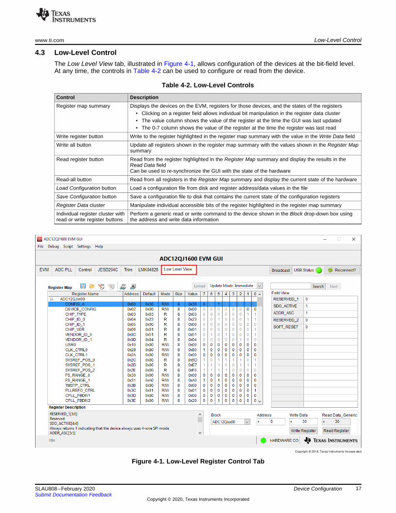
4.3 Low-Level ControlThe Low Level View tab, illustrated in Figure 4-1, allows configuration of the devices at the bit-field level.At any time, the controls in Table 4-2 can be used to configure or read from the device.
Table 4-2. Low-Level Controls
Control DescriptionRegister map summary Displays the devices on the EVM, registers for those devices, and the states of the registers
• Clicking on a register field allows individual bit manipulation in the register data cluster• The value column shows the value of the register at the time the GUI was last updated• The 0-7 column shows the value of the register at the time the register was last read
Write register button Write to the register highlighted in the register map summary with the value in the Write Data fieldWrite all button Update all registers shown in the register map summary with the values shown in the Register Map
summaryRead register button Read from the register highlighted in the Register Map summary and display the results in the
Read Data fieldCan be used to re-synchronize the GUI with the state of the hardware
Read-all button Read from all registers in the Register Map summary and display the current state of the hardwareLoad Configuration button Load a configuration file from disk and register address/data values in the fileSave Configuration button Save a configuration file to disk that contains the current state of the configuration registersRegister Data cluster Manipulate individual accessible bits of the register highlighted in the register map summaryIndividual register cluster withread or write register buttons
Perform a generic read or write command to the device shown in the Block drop-down box usingthe address and write data information
Figure 4-1. Low-Level Register Control Tab
18 SLAU808–February 2020Submit Documentation Feedback
Copyright © 2020, Texas Instruments Incorporated
Troubleshooting the ADCxxQJxx00EVM
Chapter 5SLAU808–February 2020
Troubleshooting the ADCxxQJxx00EVM
Table 5-1 lists some troubleshooting procedures.
Table 5-1. Troubleshooting
Issue Troubleshoot
General problems
• Verify the test setup shown in Figure 3-1, and repeat the setup procedure as described in thisdocument.
• Check power supply to EVM and TSW14J57EVM. Verify that the power switch is in the onposition.
• Check signal and clock connections to EVM.• Visually check the top and bottom sides of the board to verify that nothing looks discolored or
damaged.• Ensure the board-to-board FMC connection is secure.• Try pressing the CPU_RESET button on the TSW14J57EVM. Also try clicking Instrument
Options → Reset Board after changing the ADC configuration.• Try power-cycling the external power supply to the EVM, and reprogram the LMK and ADC
devices.
TSW14J57 LEDs are notcorrect
• Verify the settings of the configuration switches on the TSW14J57EVM.• Verify that the clock going to the CLK input is connected and the appropriate LEDs are blinking.• Verify that the ADC device internal registers are configured properly.• If LEDs are not blinking, reprogram the ADC EVM devices.• Try pressing the CPU_RESET button on the TSW14J57EVM.• Try capturing data in HSDC Pro to force an LED status update
Configuration GUI is notworking properly
• Verify that the USB cable is plugged into the EVM and the PC.• Check the computer device manager and verify that a USB serial device is recognized when
the EVM is connected to the PC.• Verify that the green USB Status LED light in the top right corner of the GUI is lit. If it is not lit,
click the Reconnect FTDI button.• Try restarting the configuration GUI.
Configuration GUI is notable to connect to the EVM
• Use the free FT_PROG software from FTDI chip and verify that the onboard FTDI chip isprogrammed with the product description ADC12QJxx00 or ADC09QJxx00 respectively.
HSDC Pro software is notcapturing good data oranalysis results areincorrect.
• Verify that the TSW14J57EVM is properly connected to the PC with a mini-USB cable and thatthe board serial number is properly identified by the HSDC software.
• Check that the proper ADC device mode is selected. The mode should match in HSDC Pro andthe ADC GUI.
• Check that the analysis parameters are properly configured.
HSDC Pro software gives atime-out error whencapturing data
• Try to reprogram the LMK device and reset the JESD204 link.• Verify that the ADC sampling rate is correctly set in the HSDC software.• Try pressing the CPU_RESET button on the TSW14J57EVM. Also try clicking Instrument
Options → Reset Board after changing the ADC configuration. Try to recapture again.• Select Instrument Options → Download Firmware and download
'TSW14J57RevE_16L_XCVR_ADCDDRDACBRAM.rbf'. Try to capture again.
Sub-optimal measuredperformance
• Try clicking Cal Triggered/Running button 2× to re-calibrate the ADC in the current operatingconditions. It is located on the Control tab of the configuration GUI.
• Check that the spectral analysis parameters are properly configured.• Verify that bandpass filters are used in the clock and input signal paths and that low-noise
signal sources are used.

19SLAU808–February 2020Submit Documentation Feedback
Copyright © 2020, Texas Instruments Incorporated
References
Appendix ASLAU808–February 2020
References
This section provides references to technical documents and user's guides.
A.1 Technical Reference Documents• ADC12QJ1600 datasheet• High-Speed Data Converter Pro GUI User's Guide, also available in the help menu of the software• LMK04828 data sheet• FTDI USB to Serial Driver Installation Manual
(www.ftdichip.com/Support/Documents/InstallGuides.htm)
A.2 TSW14J57EVM OperationRefer to the TSW14J57EVM user guide for configuration and status information.

20 SLAU808–February 2020Submit Documentation Feedback
Copyright © 2020, Texas Instruments Incorporated
HSDC Pro Settings for Optional ADC Device Configuration
Appendix BSLAU808–February 2020
HSDC Pro Settings for Optional ADC Device Configuration
This appendix provides settings for optional ADC device configuration in HSDC Pro.
B.1 Changing the Number of Frames per Multi-Frame (K)Changing the number of frames per multi-frame output by the JESD204 transmitter (ADC device) isconfigured using the K parameter( when using modes with 8B/10B encoding) on the JESD204C tab in theConfiguration GUI. This parameter must be matched by the receiving device, and the SYSREF frequencymust also be programmed to a compatible frequency. Ensure that the K value complies with the K Minand Step values for the selected JMODE. Refer to the ADCxxQJxx00 operating modes table in the devicedatasheet.
B.2 Customizing the EVM for Optional Clocking SupportThe ADCxxQJxx00EVM can be clocked using four different methods: Ext CLK from LMK to ADC clockingoption, Ext Direct CLK to ADC clocking option, Onboard 50M ref to ADC PLL clocking option and Ext Refto ADC PLL clocking option.
Ext CLK from LMK to ADC and Ext Direct CLK to ADC clocking options are the only two clocking optionwhich are currently supported by TSW14J57EVM capture solution. The Onboard 50M ref to ADC PLLclocking option and Ext Ref to ADC PLL requires custom firmware and FPGA Evaluation Board &Development kit hardware.

SDCLKx
SDCLKx
DCLKx
SDCLKx
DA[7:0]
SYNC
FPGA_GBT_CLK[0]
FPGA_SYSREF
CLKIN0
CLKIN1
SDCLKx
LMK04828
ADC12DJ1600
CLK
SYSREF
DA[7:0]
FMC
SYNC
Ext CLK from LMK to ADC
DCLKx
LMK00304
SDCLKx
FPGA_GBT_CLK[1]
TRIGOUT
FPGA_CLKPLLREFO
LMK CLK (J31)
500MHz -1600 MHz
Copyright © 2018, Texas Instruments Incorporated
www.ti.com Customizing the EVM for Optional Clocking Support
21SLAU808–February 2020Submit Documentation Feedback
Copyright © 2020, Texas Instruments Incorporated
HSDC Pro Settings for Optional ADC Device Configuration
B.2.1 "Ext CLK from LMK to ADC" (Default)By default, the EVM is configured to use the "Ext CLK from LMK to ADC" clock option. The user provideand external clock signal to LMK04828 at SMA connector J31 (LMK CLK). In this clocking option theLMK04828 is used in clock distribution mode and provides ADC sampling clock, the FPGA referenceclock, FPGA SYSREF signal and ADC SYSREF signal. If coherent sampling is desired the ADC analoginput signal generator and ADC sampling clock signal generator should be frequency locked to eachother. Figure B-1 shows the block diagram of external clocking option:
The EVM can be configured to use Ext CLK from LMK to ADC with the following steps (see Figure B-5):1. Modify the hardware:
a. Remove C45, C46, C2 and C3 and populate C67 and C69.
Figure B-1. ADCxxQJxx00EVM Clocking System Block Diagram

SDCLKx
SDCLKx
DCLKx
SDCLKx
DA[7:0]
SYNC
FPGA_GBT_CLK[0]
FPGA_SYSREF
CLKIN0
CLKIN1
SDCLKx
LMK04828
ADC12DJ1600
CLK
SYSREF
DA[7:0]
FMC
SYNC
Ext Direct CLK to ADC
DCLKx
LMK00304
SDCLKx
FPGA_GBT_CLK[1]
TRIGOUT
FPGA_CLKPLLREFO
FPGA Ref CLK
100MHz - 320MHz
EXT Direct CLK (J10)
500MHz ±1600MHz
Copyright © 2018, Texas Instruments Incorporated
Customizing the EVM for Optional Clocking Support www.ti.com
22 SLAU808–February 2020Submit Documentation Feedback
Copyright © 2020, Texas Instruments Incorporated
HSDC Pro Settings for Optional ADC Device Configuration
B.2.2 "Ext Direct CLK to ADC Clocking Option"The sampling clock(DEVCLK) for the ADC is provided directly from External signal generator on SMAlabeled EXT CLK(J10) . The second signal generator is used to provide the CLK to the LMK04828. TheLMK04828 is used in clock distribution mode to provides the FPGA reference clock, FPGA SYSREFsignal and ADC SYSREF signal. Ensure that the DEVCLK and FPGA Reference clock sources arefrequency-locked using a common 10-MHz reference to ensure functionality. Frequency locking the inputsignal generator to the other generators can also be done if coherent sampling is desired. Figure B-2shows the block diagram of Ext Direct CLK to ADC clocking option:
The EVM can be configured to use Ext Direct CLK to ADC clocking option with the following stepsFigure B-6:• Remove C45, C46, C67 and C69 and populate C2 and C3.
Figure B-2. Ext Direct CLK to ADC System Block Diagram
DA[7:0]
SYNC
FPGA_GBT_CLK[0]
ADC_SYSREF
ADC12DJ1600
CLK
SYSREF
DA[7:0]
FMC
SYNC
DCLKx
LMK00304
FPGA_GBT_CLK[1]
TRIGOUT
FPGA_CLKPLLREFO
50MHz
VCXO
Copyright © 2018, Texas Instruments Incorporated
SDCLKx
SDCLKx
DCLKx
SDCLKx
CLKIN0
CLKIN1
SDCLKx
LMK04828
OnBoard 50M Ref to ADC PLL
DCLKx
SDCLKx
SE_CLK
www.ti.com Customizing the EVM for Optional Clocking Support
23SLAU808–February 2020Submit Documentation Feedback
Copyright © 2020, Texas Instruments Incorporated
HSDC Pro Settings for Optional ADC Device Configuration
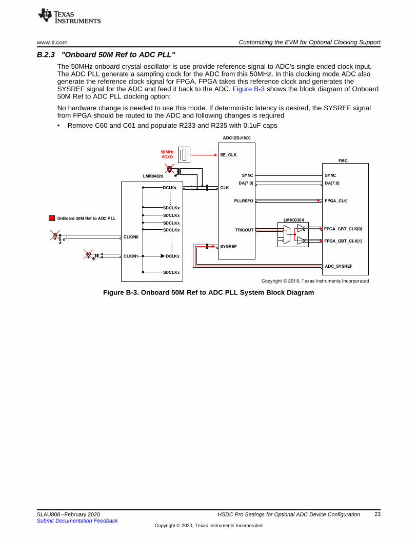
B.2.3 "Onboard 50M Ref to ADC PLL"The 50MHz onboard crystal oscillator is use provide reference signal to ADC's single ended clock input.The ADC PLL generate a sampling clock for the ADC from this 50MHz. In this clocking mode ADC alsogenerate the reference clock signal for FPGA. FPGA takes this reference clock and generates theSYSREF signal for the ADC and feed it back to the ADC. Figure B-3 shows the block diagram of Onboard50M Ref to ADC PLL clocking option:
No hardware change is needed to use this mode. If deterministic latency is desired, the SYSREF signalfrom FPGA should be routed to the ADC and following changes is required• Remove C60 and C61 and populate R233 and R235 with 0.1uF caps
Figure B-3. Onboard 50M Ref to ADC PLL System Block Diagram
DA[7:0]
SYNC
FPGA_GBT_CLK[0]
ADC_SYSREF
ADC12DJ1600
CLK
SYSREF
DA[7:0]
FMC
SYNC
DCLKx
LMK00304
FPGA_GBT_CLK[1]
TRIGOUT
FPGA_CLKPLLREFO
EXT Ref to ADC PLL
( 50MHz - 500MHz )
Copyright © 2018, Texas Instruments Incorporated
SDCLKx
SDCLKx
DCLKx
SDCLKx
CLKIN0
CLKIN1
SDCLKx
LMK04828
Ext Ref to ADC PLL
DCLKx
SDCLKx
Customizing the EVM for Optional Clocking Support www.ti.com
24 SLAU808–February 2020Submit Documentation Feedback
Copyright © 2020, Texas Instruments Incorporated
HSDC Pro Settings for Optional ADC Device Configuration
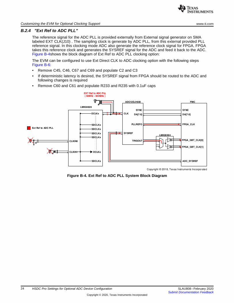
B.2.4 "Ext Ref to ADC PLL"The reference signal for the ADC PLL is provided externally from External signal generator on SMAlabeled EXT CLK(J10) . The sampling clock is generate by ADC PLL, from this external provided PLLreference signal. In this clocking mode ADC also generate the reference clock signal for FPGA. FPGAtakes this reference clock and generates the SYSREF signal for the ADC and feed it back to the ADC.Figure B-4shows the block diagram of Ext Ref to ADC PLL clocking option:
The EVM can be configured to use Ext Direct CLK to ADC clocking option with the following stepsFigure B-6:• Remove C45, C46, C67 and C69 and populate C2 and C3• If deterministic latency is desired, the SYSREF signal from FPGA should be routed to the ADC and
following changes is required• Remove C60 and C61 and populate R233 and R235 with 0.1uF caps
Figure B-4. Ext Ref to ADC PLL System Block Diagram
Copyright © 2018, Texas Instruments Incorporated
www.ti.com Customizing the EVM for Optional Clocking Support
25SLAU808–February 2020Submit Documentation Feedback
Copyright © 2020, Texas Instruments Incorporated
HSDC Pro Settings for Optional ADC Device Configuration
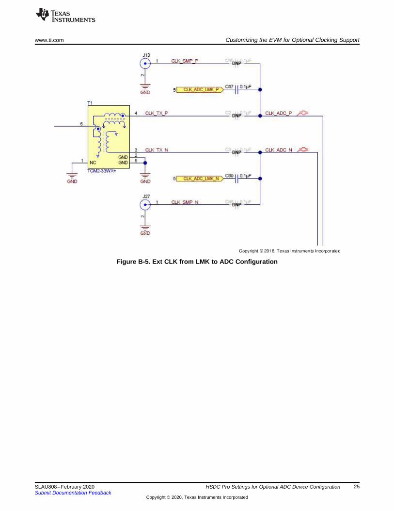
Figure B-5. Ext CLK from LMK to ADC Configuration

Copyright © 2018, Texas Instruments Incorporated
Customizing the EVM for Optional Clocking Support www.ti.com
26 SLAU808–February 2020Submit Documentation Feedback
Copyright © 2020, Texas Instruments Incorporated
HSDC Pro Settings for Optional ADC Device Configuration
Figure B-6. Ext Direct clock to ADC Configuration

27SLAU808–February 2020Submit Documentation Feedback
Copyright © 2020, Texas Instruments Incorporated
Signal Routing
Appendix CSLAU808–February 2020
Signal Routing
C.1 Signal RoutingTable C-1 provides the signal routing details for the ADCxxQJxx00EVM.
Table C-1. ADCxxQJxx00EVM Signal Routing
JESD204C Output LID FMC PinsD0 0 A10,A11D1 1 A6,A7D2 2 C6,C7D3 3 A2,A3D4 4 A18,A19D5 5 B16,B17D6 6 A14,A15D7 7 B12,B13
Copyright © 2018, Texas Instruments Incorporated
28 SLAU808–February 2020Submit Documentation Feedback
Copyright © 2020, Texas Instruments Incorporated
Analog Inputs
Appendix DSLAU808–February 2020
Analog Inputs
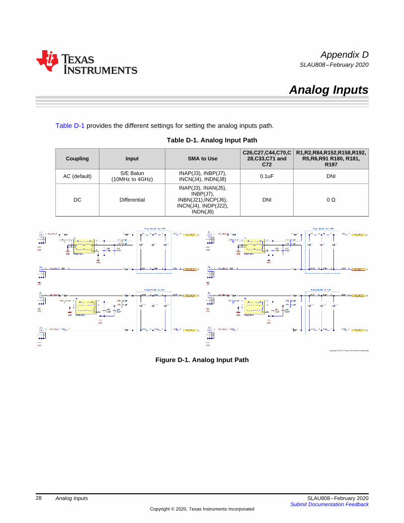
Table D-1 provides the different settings for setting the analog inputs path.
Table D-1. Analog Input Path
Coupling Input SMA to UseC26,C27,C44,C70,C
28,C33,C71 andC72
R1,R2,R84,R152,R158,R192,R5,R6,R91 R180, R181,
R197
AC (default) S/E Balun(10MHz to 4GHz)
INAP(J3), INBP(J7),INCN(J4), INDN(J8) 0.1uF DNI
DC Differential
INAP(J3), INAN(J5),INBP(J7),
INBN(J21),INCP(J6),INCN(J4), INDP(J22),
INDN(J8)
DNI 0 Ω
Figure D-1. Analog Input Path

29SLAU808–February 2020Submit Documentation Feedback
Copyright © 2020, Texas Instruments Incorporated
Jumpers and LEDs
Appendix ESLAU808–February 2020
Jumpers and LEDs
E.1 Jumper settingsTable E-1 shows the jumper settings and Table E-2 shows the LED functionality.
Table E-1. Jumper Settings
Label Description Function
J12 ADC power down jumper. Installed: ADC powered down. Uninstalled: ADC poweredup(default)
J15 Enable to 50MHz Oscillator. Installed: Oscillator Enabled(default). Uninstalled: Oscillatordisabled
J18When hardware calibration trigger option is enabled.The ADC's calibration routine is can be enable using
external signal
Installed: ADC's calibration routine is triggered. Uninstalled:ADC's calibration routine is not triggered(default).
J19 Selects the source for SPI signalsInstalled: SPI signals from FMC connector are controlling thedevices on the EVM. Uninstalled: SPI signal from the onboard
FTDI IC is controlling the devices on the EVMs(default)
J23ADC PLL enable control. When hardware pin controloption is enabled. The ADC PLL can be enabled by
setting this pin to high
Installed: ADC PLL is enabled. Uninstalled: ADC PLL isdisabled(default)
J25 FPGA GBTCLK source selection option Installed: GBTCLK is supplied by ADC's TRIGOUT signal.Uninstalled: GBTCLK is provided by the LMK04828(default).
J26 Select between single ended reference clock ordifferential reference clock or ADC PLL.
Installed: Single ended reference selected. Uninstalled:Differential reference clock is selected(default).
Table E-2. LEDs
Label FunctionD1 High temp indicatorD2 High input power on channel AD3 High input power on channel BD8 High input power on channel CD10 High input power on channel DD12 12V power is connected to the EVMD13 USB is connected to EVM

IMPORTANT NOTICE AND DISCLAIMER
TI PROVIDES TECHNICAL AND RELIABILITY DATA (INCLUDING DATASHEETS), DESIGN RESOURCES (INCLUDING REFERENCE DESIGNS), APPLICATION OR OTHER DESIGN ADVICE, WEB TOOLS, SAFETY INFORMATION, AND OTHER RESOURCES “AS IS” AND WITH ALL FAULTS, AND DISCLAIMS ALL WARRANTIES, EXPRESS AND IMPLIED, INCLUDING WITHOUT LIMITATION ANY IMPLIED WARRANTIES OF MERCHANTABILITY, FITNESS FOR A PARTICULAR PURPOSE OR NON-INFRINGEMENT OF THIRD PARTY INTELLECTUAL PROPERTY RIGHTS.These resources are intended for skilled developers designing with TI products. You are solely responsible for (1) selecting the appropriate TI products for your application, (2) designing, validating and testing your application, and (3) ensuring your application meets applicable standards, and any other safety, security, or other requirements. These resources are subject to change without notice. TI grants you permission to use these resources only for development of an application that uses the TI products described in the resource. Other reproduction and display of these resources is prohibited. No license is granted to any other TI intellectual property right or to any third party intellectual property right. TI disclaims responsibility for, and you will fully indemnify TI and its representatives against, any claims, damages, costs, losses, and liabilities arising out of your use of these resources.TI’s products are provided subject to TI’s Terms of Sale (www.ti.com/legal/termsofsale.html) or other applicable terms available either on ti.com or provided in conjunction with such TI products. TI’s provision of these resources does not expand or otherwise alter TI’s applicable warranties or warranty disclaimers for TI products.
Mailing Address: Texas Instruments, Post Office Box 655303, Dallas, Texas 75265Copyright © 2020, Texas Instruments Incorporated