Embed Size (px)
Citation preview

Automot ive Power
Data Sheet Rev. 1.0, 2015-08-12
TLE7250High Speed CAN-Transceiver
TLE7250LETLE7250SJ

Data Sheet 2 Rev. 1.0, 2015-08-12
TLE7250LETLE7250SJ
Table of Contents . . . . . . . . . . . . . . . . . . . . . . . . . . . . . . . . . . . . . . . . . . . . . . . . . . . . . . . . . . . . . . . . 2
1 Overview . . . . . . . . . . . . . . . . . . . . . . . . . . . . . . . . . . . . . . . . . . . . . . . . . . . . . . . . . . . . . . . . . . . . . . . 3
2 Block Diagram . . . . . . . . . . . . . . . . . . . . . . . . . . . . . . . . . . . . . . . . . . . . . . . . . . . . . . . . . . . . . . . . . . . 5
3 Pin Configuration . . . . . . . . . . . . . . . . . . . . . . . . . . . . . . . . . . . . . . . . . . . . . . . . . . . . . . . . . . . . . . . . 63.1 Pin Assignment . . . . . . . . . . . . . . . . . . . . . . . . . . . . . . . . . . . . . . . . . . . . . . . . . . . . . . . . . . . . . . . . . . . 63.2 Pin Definitions . . . . . . . . . . . . . . . . . . . . . . . . . . . . . . . . . . . . . . . . . . . . . . . . . . . . . . . . . . . . . . . . . . . . 6
4 Functional Description . . . . . . . . . . . . . . . . . . . . . . . . . . . . . . . . . . . . . . . . . . . . . . . . . . . . . . . . . . . . 84.1 High Speed CAN Physical Layer . . . . . . . . . . . . . . . . . . . . . . . . . . . . . . . . . . . . . . . . . . . . . . . . . . . . . 84.2 Modes of Operation . . . . . . . . . . . . . . . . . . . . . . . . . . . . . . . . . . . . . . . . . . . . . . . . . . . . . . . . . . . . . . 104.2.1 Normal-operating Mode . . . . . . . . . . . . . . . . . . . . . . . . . . . . . . . . . . . . . . . . . . . . . . . . . . . . . . . . . . 104.2.2 Power-save Mode . . . . . . . . . . . . . . . . . . . . . . . . . . . . . . . . . . . . . . . . . . . . . . . . . . . . . . . . . . . . . . 104.2.3 Receive-only Mode . . . . . . . . . . . . . . . . . . . . . . . . . . . . . . . . . . . . . . . . . . . . . . . . . . . . . . . . . . . . . 104.3 Power-up and Undervoltage Condition . . . . . . . . . . . . . . . . . . . . . . . . . . . . . . . . . . . . . . . . . . . . . . . . 114.3.1 Power-down State . . . . . . . . . . . . . . . . . . . . . . . . . . . . . . . . . . . . . . . . . . . . . . . . . . . . . . . . . . . . . . 124.3.2 Power-up . . . . . . . . . . . . . . . . . . . . . . . . . . . . . . . . . . . . . . . . . . . . . . . . . . . . . . . . . . . . . . . . . . . . . 124.3.3 Undervoltage on the Transmitter Supply VCC . . . . . . . . . . . . . . . . . . . . . . . . . . . . . . . . . . . . . . . . . 13
5 Fail Safe Functions . . . . . . . . . . . . . . . . . . . . . . . . . . . . . . . . . . . . . . . . . . . . . . . . . . . . . . . . . . . . . . 145.1 Short Circuit Protection . . . . . . . . . . . . . . . . . . . . . . . . . . . . . . . . . . . . . . . . . . . . . . . . . . . . . . . . . . . . 145.2 Unconnected Logic Pins . . . . . . . . . . . . . . . . . . . . . . . . . . . . . . . . . . . . . . . . . . . . . . . . . . . . . . . . . . . 145.3 TxD Time-out Function . . . . . . . . . . . . . . . . . . . . . . . . . . . . . . . . . . . . . . . . . . . . . . . . . . . . . . . . . . . . 145.4 Overtemperature Protection . . . . . . . . . . . . . . . . . . . . . . . . . . . . . . . . . . . . . . . . . . . . . . . . . . . . . . . . 155.5 Delay Time for Mode Change . . . . . . . . . . . . . . . . . . . . . . . . . . . . . . . . . . . . . . . . . . . . . . . . . . . . . . . 15
6 General Product Characteristics . . . . . . . . . . . . . . . . . . . . . . . . . . . . . . . . . . . . . . . . . . . . . . . . . . . 166.1 Absolute Maximum Ratings . . . . . . . . . . . . . . . . . . . . . . . . . . . . . . . . . . . . . . . . . . . . . . . . . . . . . . . . 166.2 Functional Range . . . . . . . . . . . . . . . . . . . . . . . . . . . . . . . . . . . . . . . . . . . . . . . . . . . . . . . . . . . . . . . . 176.3 Thermal Resistance . . . . . . . . . . . . . . . . . . . . . . . . . . . . . . . . . . . . . . . . . . . . . . . . . . . . . . . . . . . . . . 17
7 Electrical Characteristics . . . . . . . . . . . . . . . . . . . . . . . . . . . . . . . . . . . . . . . . . . . . . . . . . . . . . . . . . 187.1 Functional Device Characteristics . . . . . . . . . . . . . . . . . . . . . . . . . . . . . . . . . . . . . . . . . . . . . . . . . . . 187.2 Diagrams . . . . . . . . . . . . . . . . . . . . . . . . . . . . . . . . . . . . . . . . . . . . . . . . . . . . . . . . . . . . . . . . . . . . . . 23
8 Application Information . . . . . . . . . . . . . . . . . . . . . . . . . . . . . . . . . . . . . . . . . . . . . . . . . . . . . . . . . . 258.1 ESD Robustness according to IEC61000-4-2 . . . . . . . . . . . . . . . . . . . . . . . . . . . . . . . . . . . . . . . . . . 258.2 Application Example . . . . . . . . . . . . . . . . . . . . . . . . . . . . . . . . . . . . . . . . . . . . . . . . . . . . . . . . . . . . . . 268.3 Examples for Mode Changes . . . . . . . . . . . . . . . . . . . . . . . . . . . . . . . . . . . . . . . . . . . . . . . . . . . . . . . 278.3.1 Mode Change while the TxD Signal is “low” . . . . . . . . . . . . . . . . . . . . . . . . . . . . . . . . . . . . . . . . . . 288.3.2 Mode Change while the Bus Signal is “dominant” . . . . . . . . . . . . . . . . . . . . . . . . . . . . . . . . . . . . . . 288.4 Further Application Information . . . . . . . . . . . . . . . . . . . . . . . . . . . . . . . . . . . . . . . . . . . . . . . . . . . . . . 31
9 Package Outline . . . . . . . . . . . . . . . . . . . . . . . . . . . . . . . . . . . . . . . . . . . . . . . . . . . . . . . . . . . . . . . . 32
10 Revision History . . . . . . . . . . . . . . . . . . . . . . . . . . . . . . . . . . . . . . . . . . . . . . . . . . . . . . . . . . . . . . . . 33
Table of Contents

Type Package MarkingTLE7250LE PG-TSON-8 7250TLE7250SJ PG-DSO-8 7250
PG-TSON-8
PG-DSO-8
Data Sheet 3 Rev. 1.0, 2015-08-12
High Speed CAN-Transceiver TLE7250LETLE7250SJ
1 Overview
Features• Fully compatible to ISO 11898-2• Wide common mode range for electromagnetic immunity (EMI)• Very low electromagnetic emission (EME)• Excellent ESD robustness• Guaranteed loop delay symmetry to support CAN FD data frames up
to 2 MBit/s• Extended supply range on VCC supply• CAN short circuit proof to ground, battery and VCC
• TxD time-out function• Low CAN bus leakage current in power-down state• Overtemperature protection• Protected against automotive transients• Receive-only mode and power-save mode• Green Product (RoHS compliant)• Two package variants: PG-DSO-8 and PG-TSON-8• AEC Qualified
DescriptionThe TLE7250 is a transceiver designed for HS CAN networks inautomotive and industrial applications. As an interface between the physical bus layer and the CAN protocolcontroller, the TLE7250 drives the signals to the bus and protects the microcontroller against interferencesgenerated within the network. Based on the high symmetry of the CANH and CANL signals, the TLE7250 providesa very low level of electromagnetic emission (EME) within a wide frequency range.The TLE7250 is available in a small, leadless PG-TSON-8 package and in a PG-DSO-8 package. Both packagesare RoHS compliant and halogen free. Additionally the PG-TSON-8 package supports the solder jointrequirements for automated optical inspection (AOI). The TLE7250LE and the TLE7250SJ are fulfilling orexceeding the requirements of the ISO11898-2. The TLE7250 provides a receive-only mode and a power-save mode. It is designed to fulfill the enhanced physicallayer requirements for CAN FD and supports data rates up to 2 MBit/s.On the basis of a very low leakage current on the HS CAN bus interface the TLE7250 provides an excellentpassive behavior in power-down state. These and other features make the TLE7250 exceptionally suitable formixed supply HS CAN networks.Based on the Infineon Smart Power Technology SPT, the TLE7250 provides excellent ESD immunity together with
TLE7250LETLE7250SJ
Overview
Data Sheet 4 Rev. 1.0, 2015-08-12
a very high electromagnetic immunity (EMI). The TLE7250 and the Infineon SPT technology are AEC qualifiedand tailored to withstand the harsh conditions of the automotive environment.Three different operating modes, additional fail-safe features like a TxD time-out and the optimized outputslew rates on the CANH and CANL signals, make the TLE7250 the ideal choice for large HS CAN networks withhigh data transmission rates.
TLE7250LETLE7250SJ
Block Diagram
Data Sheet 5 Rev. 1.0, 2015-08-12
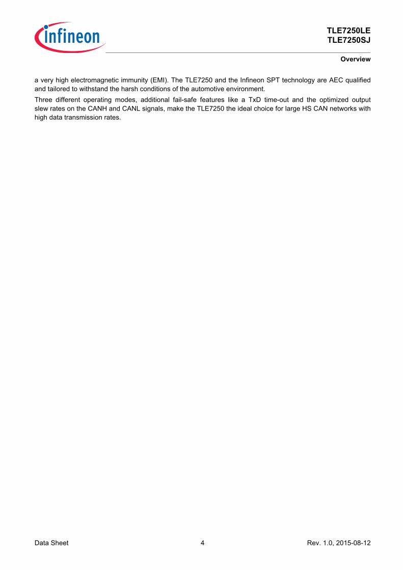
2 Block Diagram
Figure 1 Functional block diagram
Driver
Temp-protection
Modecontrol
7CANH
6CANL
2GND
TxD
3VCC
NEN
RxD
Timeout
Transmitter
Receiver
VCC/2
Normal-mode receiver
1
8
4
Bus-biasing
=
NRM5

TLE7250LETLE7250SJ
Pin Configuration
Data Sheet 6 Rev. 1.0, 2015-08-12
3 Pin Configuration
3.1 Pin Assignment
Figure 2 Pin configuration
3.2 Pin Definitions
Table 1 Pin definitions and functionsPin No. Symbol Function1 TxD Transmit Data Input;
internal pull-up to VCC, “low” for “dominant” state.2 GND Ground3 VCC Transmitter Supply Voltage;
100 nF decoupling capacitor to GND required.4 RxD Receive Data Output;
“low” in “dominant” state.5 NRM Not Receive-Only Mode Input;
control input for selecting receive-only mode,internal pull-up to VCC, “low” for receive-only mode.
6 CANL CAN Bus Low Level I/O;“low” in “dominant” state.
7 CANH CAN Bus High Level I/O; “high” in “dominant” state.
TxD NEN
NRM
1
2
3
4
8
7
6
5
GND
VCC
RxD
CANH
CANL
1
2
3
4
8
7
6
5
TxD
GND
VCC
RxD
NEN
NRM
CANH
CANL
(Top-side x-ray view)
PAD

TLE7250LETLE7250SJ
Pin Configuration
Data Sheet 7 Rev. 1.0, 2015-08-12
8 NEN Not Enable Input;internal pull-up to VCC, “low” for normal-operating mode or receive-only mode.
PAD – Connect to PCB heat sink area. Do not connect to other potential than GND.
Table 1 Pin definitions and functions (cont’d)Pin No. Symbol Function

TLE7250LETLE7250SJ
Functional Description
Data Sheet 8 Rev. 1.0, 2015-08-12
4 Functional DescriptionHS CAN is a serial bus system that connects microcontrollers, sensors and actuators for real-time controlapplications. The use of the Controller Area Network (abbreviated CAN) within road vehicles is described by theinternational standard ISO 11898. According to the 7-layer OSI reference model the physical layer of a HS CANbus system specifies the data transmission from one CAN node to all other available CAN nodes within thenetwork. The physical layer specification of a CAN bus system includes all electrical and mechanical specificationsof a CAN network. The CAN transceiver is part of the physical layer specification. Several different physical layerstandards of CAN networks have been developed in recent years. The TLE7250 is a High Speed CAN transceiverwithout a wake-up function and defined by the international standard ISO11898-2.
4.1 High Speed CAN Physical Layer
Figure 3 High speed CAN bus signals and logic signals
TxDVCC
t
t
VCCCANHCANL
t
VCCVDiff
RxDVCC
t
VCC = Transmitter supply voltage TxD = Transmit data input from
the microcontroller RxD = Receive data output to
the microcontrollerCANH = Bus level on the CANH
input/output CANL = Bus level on the CANL
input/output VDiff = Differential voltage between CANH and CANL
VDiff = VCANH – VCANL
“dominant” receiver threshold
“recessive” receiver threshold
tLoop(H,L) tLoop(L,H)

TLE7250LETLE7250SJ
Functional Description
Data Sheet 9 Rev. 1.0, 2015-08-12
The TLE7250 is a High-Speed CAN transceiver, operating as an interface between the CAN controller and thephysical bus medium. A HS CAN network is a two wire, differential network which allows data transmission ratesfor CAN FD frames up to 2 MBit/s. Characteristic for HS CAN networks are the two signal states on the HS CANbus: “dominant” and “recessive” (see Figure 3). VCC and GND are the supply pins for the TLE7250. The pins CANH and CANL are the interface to the HS CANbus and operate in both directions, as an input and as an output. RxD and TxD pins are the interface to the CANcontroller, the TxD pin is an input pin and the RxD pin is an output pin. The NEN and NRM pins are the input pinsfor the mode selection (see Figure 4). By setting the TxD input pin to logical “low” the transmitter of the TLE7250 drives a “dominant” signal to the CANHand CANL pins. Setting TxD input to logical “high” turns off the transmitter and the output voltage on CANH andCANL discharges towards the “recessive” level. The “recessive” output voltage is provided by the bus-biasing (seeFigure 1). The output of the transmitter is considered to be “dominant”, when the voltage difference betweenCANH and CANL is at least higher than 1.5 V (VDiff = VCANH - VCANL).Parallel to the transmitter the normal-mode receiver monitors the signal on the CANH and CANL pins and indicatesit on the RxD output pin. A “dominant” signal on the CANH and CANL pins sets the RxD output pin to logical “low”,vice versa a “recessive” signal sets the RxD output to logical “high”. The normal-mode receiver considers a voltagedifference (VDiff) between CANH and CANL above 0.9 V as “dominant” and below 0.5 V as “recessive”.To be conform with HS CAN features, like the bit to bit arbitration, the signal on the RxD output has to follow thesignal on the TxD input within a defined loop delay tLoop ≤ 255 ns.

TLE7250LETLE7250SJ
Functional Description
Data Sheet 10 Rev. 1.0, 2015-08-12
4.2 Modes of OperationThe TLE7250 supports three different modes of operation, power-save mode, receive-only mode and normal-operating mode while the transceiver is supplied according to the specified functional range. The mode ofoperation is selected by the NEN and the NRM input pins (see Figure 4).
Figure 4 Mode state diagram
4.2.1 Normal-operating ModeIn normal-operating mode the transmitter and the receiver of the HS CAN transceiver TLE7250 are active (seeFigure 1). The HS CAN transceiver sends the serial data stream on the TxD input pin to the CAN bus. The dataon the CAN bus is displayed at the RxD pin simultaneously. A logical “low” signal on the NEN pin and a logical“high” signal on the NRM pin selects the normal-operating mode, while the transceiver is supplied by VCC (seeTable 2 for details).
4.2.2 Power-save ModeThe power-save mode is an idle mode of the TLE7250 with optimized power consumption. In power-save modethe transmitter and the normal-mode receiver are turned off. The TLE7250 can not send any data to the HS CANbus nor receive any data from the HS CAN bus. The RxD output pin is permanently “high” in the power-save mode.A logical “high” signal on the NEN pin selects the power-save mode, while the transceiver is supplied by thetransmitter supply VCC (see Table 2 for details).In power-save mode the bus input pins are not biased. Therefore the CANH and CANL input pins are floating andthe HS CAN bus interface has a high resistance.
4.2.3 Receive-only ModeIn receive-only mode the normal-mode receiver is active and the transmitter is turned off. The TLE7250 canreceive data from the HS CAN bus, but cannot send any data to the HS CAN bus. A logical “low” signal on the NEN pin and a logical “low” signal on the NRM pin selects the receive-only mode,while the transceiver is supplied by VCC (see Table 2 for details).
power-save mode
NEN = 0
VCC > VCC(UV,R)
NEN = 1 NRM = “X”
normal-operating mode
NEN = 0 NRM = 1
receive-only mode
NEN = 0 NRM = 0
VCC > VCC(UV,R) VCC > VCC(UV,R)
NRM = 0
NEN = 0NRM = 1
NEN = 0NRM = 1
NEN = 1NRM = “X”
NEN = 0NRM = 0
NEN = 1NRM = “X”

TLE7250LETLE7250SJ
Functional Description
Data Sheet 11 Rev. 1.0, 2015-08-12
4.3 Power-up and Undervoltage ConditionBy detecting an undervoltage event or by switching off the transmitter power supply VCC, the transceiver TLE7250changes the mode of operation (details see Figure 5).
Figure 5 Power-up and undervoltage
Table 2 Modes of operationMode NEN NRM VCC Bus-bias Transmitter Normal-mode
ReceiverLow-power Receiver
Normal-operating “low” “high” “on” VCC/2 “on” “on” not availablePower-save “high” “X” “on” floating “off” “off” not availableReceive-only “low” “low” “on” VCC/2 “off” “on” not availablePower-down state “X” “X” “off” floating “off” “off” not available
NEN NRM VCC
power-down state
“X”“X” “off”
normal-operating mode
NEN NRM VCC
0 1 “on”
receive-only mode
NEN NRM VCC
0 0 “on”
power-save mode
NEN NRM VCC
1 “X” “on”
VCC “on”NEN “1”NRM “X”
VCC “on”NEN “0”NRM “1”
VCC “on”NEN “0”NRM “0”
VCC “on”NEN “0”NRM “X”
VCC “on”NEN “0”NRM “1”
VCC “on”NEN “1”NRM “X”
VCC “on”NEN “0”NRM “0”
VCC “on”NEN “0”NRM “0”
VCC “on”NEN “0”NRM “1”

TLE7250LETLE7250SJ
Functional Description
Data Sheet 12 Rev. 1.0, 2015-08-12
4.3.1 Power-down StateIndependent of the NEN and NRM input pins the TLE7250 is in power-down state when the transmitter supplyvoltage VCC is turned off (see Figure 5). In the power-down state the input resistors of the receiver are disconnected from the bus biasing VCC/2. The CANHand CANL bus interface of the TLE7250 is floating and acts as a high-impedance input with a very small leakagecurrent. The high-ohmic input does not influence the “recessive” level of the CAN network and allows an optimizedEME performance of the entire HS CAN network (see also Table 2).
4.3.2 Power-upThe HS CAN transceiver TLE7250 powers up if the transmitter supply VCC is connected to the device. By defaultthe device powers up in power-save mode, due to the internal pull-up resistor on the NEN pin to VCC. In case the device needs to power-up to normal-operating mode, the NEN pin needs to be pulled active to logical“low” while the NRM pin is logical “high” (see Figure 5).
TLE7250LETLE7250SJ
Functional Description
Data Sheet 13 Rev. 1.0, 2015-08-12
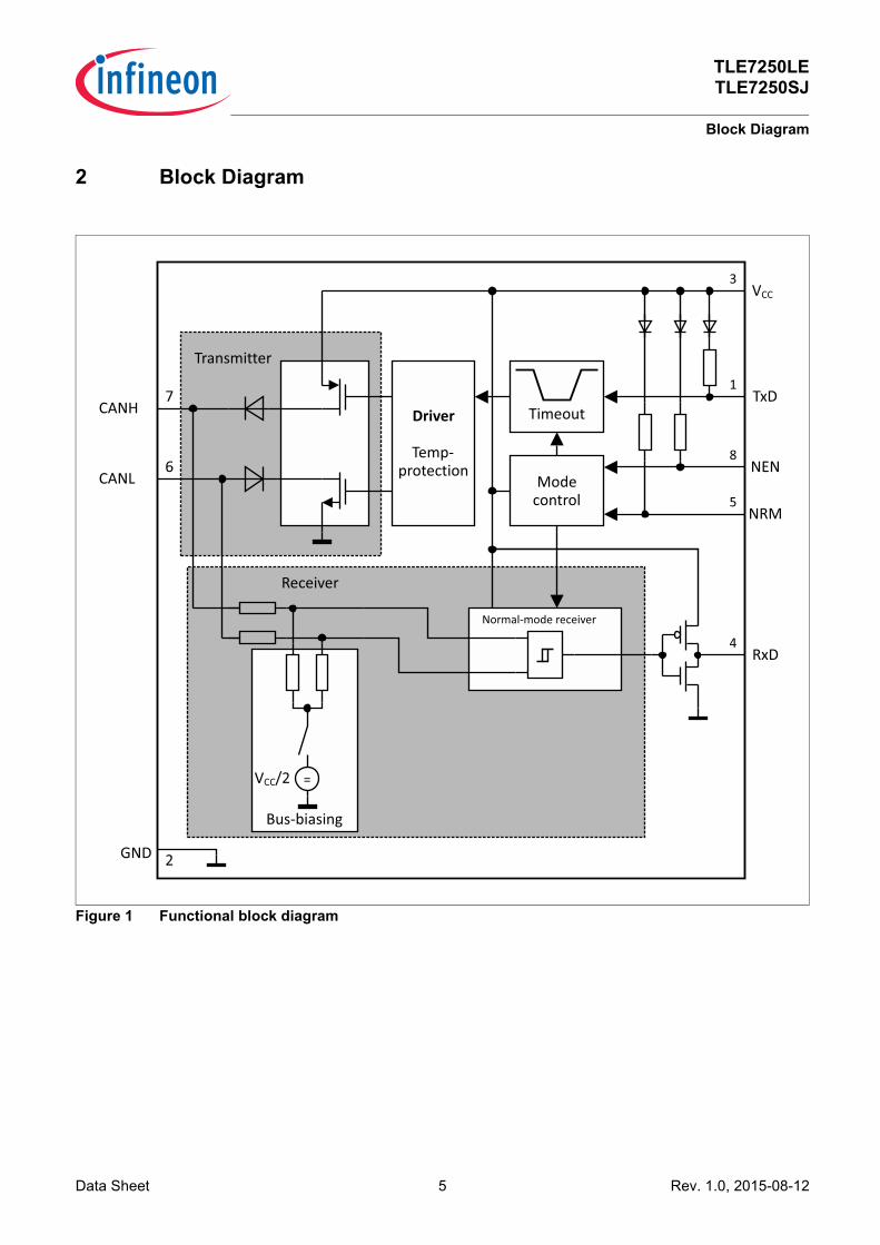
4.3.3 Undervoltage on the Transmitter Supply VCCIn case the transmitter supply VCC falls below the threshold VCC < VCC(UV,F), the transceiver TLE7250 can notprovide the correct bus levels to the CANH and CANL anymore. The normal-mode receiver is powered by thetransmitter supply VCC. In case of insufficient VCC supply the TLE7250 can neither transmit the CANH and CANLsignals correctly to bus nor can it receive them properly. Therefore the TLE7250 powers down and blocks both,the transmitter and the receiver. The transceiver TLE7250 powers up again, when the transmitter supply VCC recovers from the undervoltagecondition.
Figure 6 Undervoltage on the transmitter supply VCC
power-down state
tDelay(UV) delay time undervoltage
any mode of operation
VCC
hysteresis VCC(UV,H)
t
power-save mode
t
NEN
“X” = don’t care “high” due the internal pull-up resistor1)
VCC undervoltage monitor VCC(UV,F)
VCC undervoltage monitor VCC(UV,R)
t
NRM
“X” = don’t care “high” due the internal pull-up resistor1)
1) assuming no external signal applied

TLE7250LETLE7250SJ
Fail Safe Functions
Data Sheet 14 Rev. 1.0, 2015-08-12
5 Fail Safe Functions
5.1 Short Circuit ProtectionThe CANH and CANL bus outputs are short circuit proof, either against GND or a positive supply voltage. A currentlimiting circuit protects the transceiver against damages. If the device is heating up due to a continuous short onthe CANH or CANL, the internal overtemperature protection switches off the bus transmitter.
5.2 Unconnected Logic PinsAll logic input pins have an internal pull-up resistor to VCC. In case the VCC supply is activated and the logical pinsare open, the TLE7250 enters into the power-save mode by default. In power-save mode the transmitter of theTLE7250 is disabled and the bus bias is floating.
5.3 TxD Time-out FunctionThe TxD time-out feature protects the CAN bus against permanent blocking in case the logical signal on the TxDpin is continuously “low”. A continuous “low” signal on the TxD pin might have its root cause in a locked-upmicrocontroller or in a short circuit on the printed circuit board, for example. In normal-operating mode, a logical“low” signal on the TxD pin for the time t > tTxD enables the TxD time-out feature and the TLE7250 disables thetransmitter (see Figure 7). The receiver is still active and the data on the bus continues to be monitored by theRxD output pin.
Figure 7 TxD time-out function
Figure 7 illustrates how the transmitter is deactivated and activated again. A permanent “low” signal on the TxDinput pin activates the TxD time-out function and deactivates the transmitter. To release the transmitter after a TxDtime-out event the TLE7250 requires a signal change on the TxD input pin from logical “low” to logical “high”.
TxD
t
t
CANHCANL
RxD
t
TxD time-out TxD time–out releasedt > tTxD

TLE7250LETLE7250SJ
Fail Safe Functions
Data Sheet 15 Rev. 1.0, 2015-08-12
5.4 Overtemperature ProtectionThe TLE7250 has an integrated overtemperature detection to protect the TLE7250 against thermal overstress ofthe transmitter. The overtemperature protection is active in normal-operating mode and disabled in power-savemode and receive-only mode. In case of an overtemperature condition, the temperature sensor will disable thetransmitter (see Figure 1) while the transceiver remains in normal-operating mode.After the device has cooled down the transmitter is activated again (see Figure 8). A hysteresis is implementedwithin the temperature sensor.
Figure 8 Overtemperature protection
5.5 Delay Time for Mode ChangeThe HS CAN transceiver TLE7250 changes the mode of operation within the time window tMode. Depending on theselected mode of operation, the RxD output pin is set to logical “high” during the mode change. In this case the RxD output does not reflect the status on the CANH and CANL input pins (see as an exampleFigure 13 and Figure 14).
TxD
t
t
CANHCANL
RxD
t
TJ
t
TJSD (shut down temperature)
switch-on transmitter
T
cool down

TLE7250LETLE7250SJ
General Product Characteristics
Data Sheet 16 Rev. 1.0, 2015-08-12
6 General Product Characteristics
6.1 Absolute Maximum Ratings
Note: Stresses above the ones listed here may cause permanent damage to the device. Exposure to absolute maximum rating conditions for extended periods may affect device reliability. Integrated protection functions are designed to prevent IC destruction under fault conditions described in the data sheet. Fault conditions are considered as “outside” normal-operating range. Protection functions are not designed for continuos repetitive operation.
Table 3 Absolute maximum ratings voltages, currents and temperatures1)
All voltages with respect to ground; positive current flowing into pin;(unless otherwise specified)
1) Not subject to production test, specified by design
Parameter Symbol Values Unit Note / Test Condition
NumberMin. Typ. Max.
VoltagesTransmitter supply voltage VCC -0.3 – 6.0 V – P_6.1.1CANH DC voltage versus GND VCANH -40 – 40 V – P_6.1.2CANL DC voltage versus GND VCANL -40 – 40 V – P_6.1.3Differential voltage between CANH and CANL
VCAN SDiff -40 – 40 V – P_6.1.4
Voltages at the input pins:NEN, NRM, TxD
VMAX_IN -0.3 – 6.0 V – P_6.1.5
Voltages at the output pin:RxD
VMAX_OUT -0.3 – VCC V – P_6.1.6
CurrentsRxD output current IRxD -20 – 20 mA – P_6.1.7TemperaturesJunction temperature Tj -40 – 150 °C – P_6.1.8Storage temperature TS -55 – 150 °C – P_6.1.9ESD ResistivityESD immunity at CANH, CANL versus GND
VESD_HBM_
CAN
-9 – 9 kV HBM(100 pF via 1.5 kΩ)2)
2) ESD susceptibility, Human Body Model “HBM” according to ANSI/ESDA/JEDEC JS-001
P_6.1.10
ESD immunity at all other pins VESD_HBM_
ALL
-2 – 2 kV HBM(100 pF via 1.5 kΩ)2)
P_6.1.11
ESD immunity to GND VESD_CDM -750 – 750 V CDM3)
3) ESD susceptibility, Charge Device Model “CDM” according to EIA/JESD22-C101 or ESDA STM5.3.1
P_6.1.12

TLE7250LETLE7250SJ
General Product Characteristics
Data Sheet 17 Rev. 1.0, 2015-08-12
6.2 Functional Range
Note: Within the functional range the IC operates as described in the circuit description. The electrical characteristics are specified within the conditions given in the related electrical characteristics table.
6.3 Thermal Resistance
Note: This thermal data was generated in accordance with JEDEC JESD51 standards. For more information, please visit www.jedec.org.
Table 4 Functional rangeParameter Symbol Values Unit Note /
Test ConditionNumber
Min. Typ. Max.Supply VoltagesTransmitter supply voltage VCC 4.5 – 5.5 V – P_6.2.1Thermal ParametersJunction temperature Tj -40 – 150 °C 1)
1) Not subject to production test, specified by design.P_6.2.2
Table 5 Thermal resistance1)
1) Not subject to production test, specified by design
Parameter Symbol Values Unit Note / Test Condition
NumberMin. Typ. Max.
Thermal ResistancesJunction to Ambient PG-TSON-8 RthJA – 55 – K/W 2) TLE7250LE
2) Specified RthJA value is according to Jedec JESD51-2,-7 at natural convection on FR4 2s2p board. The product (TLE7250) was simulated on a 76.2 x 114.3 x 1.5 mm board with 2 inner copper layers (2 x 70µm Cu, 2 x 35µm Cu).
P_6.3.1Junction to Ambient PG-DSO-8 RthJA – 130 – K/W 2) TLE7250SJ P_6.3.4Thermal Shutdown (junction temperature)Thermal shutdown temperature TJSD 150 175 200 °C – P_6.3.2Thermal shutdown hysteresis ∆T – 10 – K – P_6.3.3

TLE7250LETLE7250SJ
Electrical Characteristics
Data Sheet 18 Rev. 1.0, 2015-08-12
7 Electrical Characteristics
7.1 Functional Device Characteristics
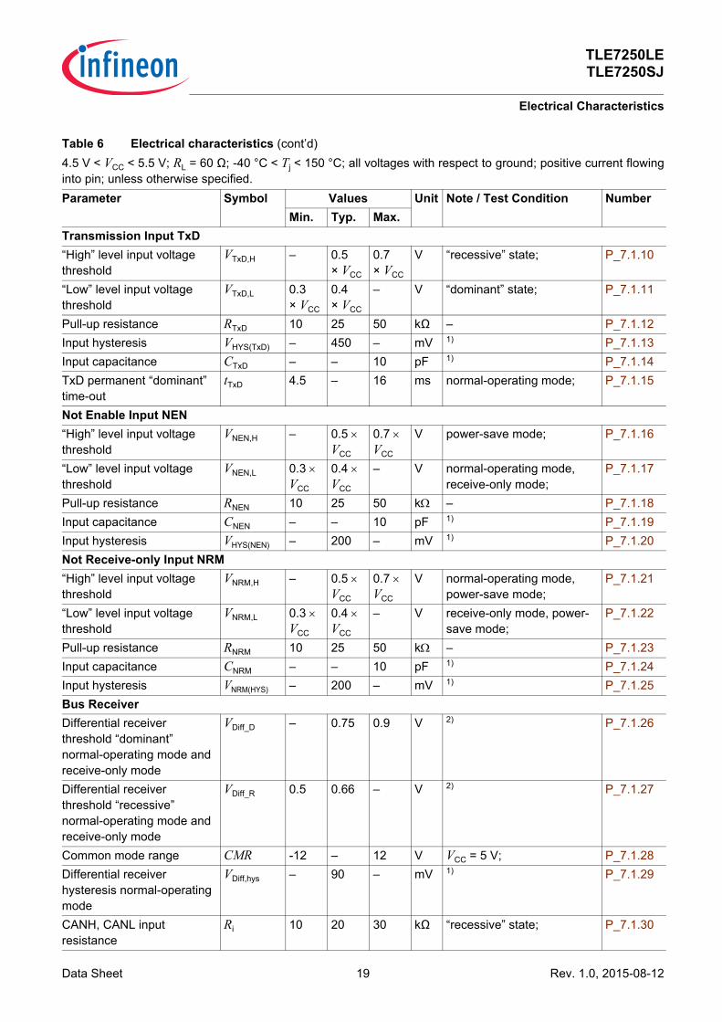
Table 6 Electrical characteristics4.5 V < VCC < 5.5 V; RL = 60 Ω; -40 °C < Tj < 150 °C; all voltages with respect to ground; positive current flowinginto pin; unless otherwise specified.Parameter Symbol Values Unit Note / Test Condition Number
Min. Typ. Max.Current ConsumptionCurrent consumption at VCCnormal-operating mode
ICC – 2.6 5 mA “recessive” state,VTxD = VNRM = VCC, VNEN = 0 V;
P_7.1.1
Current consumption at VCC normal-operating mode
ICC – 38 60 mA “dominant” state, VTxD = VNEN = 0 V, VNRM = VCC;
P_7.1.2
Current consumption at VCC receive-only mode
ICC(ROM) – 2 3 mA VNEN = VNRM = 0 V; P_7.1.3
Current consumption at VCC power-save mode
ICC(PSM) – 5 12 µA VTxD = VNEN = VNRM = VCC; P_7.1.4
Supply ResetsVCC undervoltage monitorrising edge
VCC(UV,R) 3.8 4.0 4.3 V – P_7.1.5
VCC undervoltage monitorfalling edge
VCC(UV,F) 3.65 3.85 4.3 V – P_7.1.52
VCC undervoltage monitorhysteresis
VCC(UV,H) – 150 – mV 1) P_7.1.6
VCC undervoltage delay time tDelay(UV) – – 100 µs 1) (see Figure 6); P_7.1.7Receiver Output RxD“High” level output current IRD,H – -4 -2 mA VRxD = VCC - 0.4 V,
VDiff < 0.5 V; P_7.1.8
“Low” level output current IRD,L 2 4 – mA VRxD = 0.4 V, VDiff > 0.9 V; P_7.1.9
TLE7250LETLE7250SJ
Electrical Characteristics
Data Sheet 19 Rev. 1.0, 2015-08-12
Transmission Input TxD“High” level input voltage threshold
VTxD,H – 0.5 × VCC
0.7 × VCC
V “recessive” state; P_7.1.10
“Low” level input voltage threshold
VTxD,L 0.3 × VCC
0.4 × VCC
– V “dominant” state; P_7.1.11
Pull-up resistance RTxD 10 25 50 kΩ – P_7.1.12Input hysteresis VHYS(TxD) – 450 – mV 1) P_7.1.13Input capacitance CTxD – – 10 pF 1) P_7.1.14TxD permanent “dominant” time-out
tTxD 4.5 – 16 ms normal-operating mode; P_7.1.15
Not Enable Input NEN“High” level input voltage threshold
VNEN,H – 0.5 × VCC
0.7 × VCC
V power-save mode; P_7.1.16
“Low” level input voltage threshold
VNEN,L 0.3 × VCC
0.4 × VCC
– V normal-operating mode, receive-only mode;
P_7.1.17
Pull-up resistance RNEN 10 25 50 kΩ – P_7.1.18Input capacitance CNEN – – 10 pF 1) P_7.1.19Input hysteresis VHYS(NEN) – 200 – mV 1) P_7.1.20Not Receive-only Input NRM“High” level input voltage threshold
VNRM,H – 0.5 × VCC
0.7 × VCC
V normal-operating mode, power-save mode;
P_7.1.21
“Low” level input voltage threshold
VNRM,L 0.3 × VCC
0.4 × VCC
– V receive-only mode, power-save mode;
P_7.1.22
Pull-up resistance RNRM 10 25 50 kΩ – P_7.1.23Input capacitance CNRM – – 10 pF 1) P_7.1.24Input hysteresis VNRM(HYS) – 200 – mV 1) P_7.1.25Bus ReceiverDifferential receiver threshold “dominant”normal-operating mode and receive-only mode
VDiff_D – 0.75 0.9 V 2) P_7.1.26
Differential receiver threshold “recessive”normal-operating mode and receive-only mode
VDiff_R 0.5 0.66 – V 2) P_7.1.27
Common mode range CMR -12 – 12 V VCC = 5 V; P_7.1.28Differential receiver hysteresis normal-operating mode
VDiff,hys – 90 – mV 1) P_7.1.29
CANH, CANL input resistance
Ri 10 20 30 kΩ “recessive” state; P_7.1.30
Table 6 Electrical characteristics (cont’d)4.5 V < VCC < 5.5 V; RL = 60 Ω; -40 °C < Tj < 150 °C; all voltages with respect to ground; positive current flowinginto pin; unless otherwise specified.Parameter Symbol Values Unit Note / Test Condition Number
Min. Typ. Max.

TLE7250LETLE7250SJ
Electrical Characteristics
Data Sheet 20 Rev. 1.0, 2015-08-12
Differential input resistance RDiff 20 40 60 kΩ “recessive” state; P_7.1.31Input resistance deviation between CANH and CANL
∆Ri - 1 – 1 % 1) “recessive” state; P_7.1.32
Input capacitance CANH, CANL versus GND
CIn – 20 40 pF 1) VTxD = VCC; P_7.1.33
Differential input capacitance CInDiff – 10 20 pF 1) VTxD = VCC; P_7.1.34Bus TransmitterCANL/CANH “recessive” output voltagenormal-operating mode
VCANL/H 2.0 2.5 3.0 V VTxD = VCC, no load;
P_7.1.35
CANH, CANL “recessive” output voltage differencenormal-operating mode
VDiff_NM -500 – 50 mV VTxD = VCC,no load;
P_7.1.36
CANL “dominant”output voltagenormal-operating mode
VCANL 0.5 – 2.25 V VTxD = 0 V; P_7.1.37
CANH “dominant”output voltagenormal-operating mode
VCANH 2.75 – 4.5 V VTxD = 0 V; P_7.1.38
CANH, CANL “dominant” output voltage differencenormal-operating mode according to ISO 11898-2 VDiff = VCANH - VCANL
VDiff 1.5 – 3.0 V VTxD = 0 V, 50 Ω < RL < 65 Ω, 4.75 < VCC < 5.25 V;
P_7.1.39
CANH, CANL “dominant” output voltage differencenormal-operating mode VDiff = VCANH - VCANL
VDiff_R45 1.4 – 3.0 V VTxD = 0 V, 45 Ω < RL < 50 Ω, 4.75 < VCC < 5.25 V;
P_7.1.53
Driver “dominant” symmetry normal-operating mode VSYM = VCANH + VCANL
VSYM 4.5 5 5.5 V VCC = 5.0 V, VTxD = 0 V; P_7.1.40
CANL short circuit current ICANLsc 40 75 100 mA VCANLshort = 18 V, VCC = 5.0 V, t < tTxD, VTxD = 0 V;
P_7.1.41
CANH short circuit current ICANHsc -100 -75 -40 mA VCANHshort = 0 V, VCC = 5.0 V, t < tTxD,VTxD = 0 V;
P_7.1.42
Leakage current, CANH ICANH,lk -5 – 5 µA VCC = 0 V,0 V < VCANH < 5 V, VCANH=VCANL;
P_7.1.43
Table 6 Electrical characteristics (cont’d)4.5 V < VCC < 5.5 V; RL = 60 Ω; -40 °C < Tj < 150 °C; all voltages with respect to ground; positive current flowinginto pin; unless otherwise specified.Parameter Symbol Values Unit Note / Test Condition Number
Min. Typ. Max.

TLE7250LETLE7250SJ
Electrical Characteristics
Data Sheet 21 Rev. 1.0, 2015-08-12
Leakage current, CANL ICANL,lk -5 – 5 µA VCC = 0 V, 0 V < VCANL < 5 V, VCANH=VCANL;
P_7.1.44
Dynamic CAN-Transceiver CharacteristicsPropagation delayTxD-to-RxD “low” (“recessive to “dominant”)
tLoop(H,L) – 180 255 ns CL = 100 pF, 4.75 V < VCC < 5.25 V,CRxD = 15 pF;
P_7.1.45
Propagation delayTxD-to-RxD “high”(“dominant” to “recessive”)
tLoop(L,H) – 180 255 ns CL = 100 pF, 4.75 V < VCC < 5.25 V,CRxD = 15 pF;
P_7.1.46
Propagation delay extended loadTxD-to-RxD “low”(“recessive to “dominant”)
tLoop_Ext(H,L) – – 300 ns 1) CL = 200 pF, RL = 120 Ω, 4.75 V < VCC < 5.25 V,CRxD = 15 pF;
P_7.1.54
Propagation delayextended loadTxD-to-RxD “high”(“dominant” to “recessive”)
tLoop_Ext(L,H) – – 300 ns 1) CL = 200 pF, RL = 120 Ω, 4.75 V < VCC < 5.25 V,CRxD = 15 pF;
P_7.1.55
Propagation delayTxD “low” to bus “dominant”
td(L),T – 90 140 ns CL = 100 pF, 4.75 V < VCC < 5.25 V,CRxD = 15 pF;
P_7.1.47
Propagation delayTxD “high” to bus “recessive”
td(H),T – 90 140 ns CL = 100 pF, 4.75 V < VCC < 5.25 V,CRxD = 15 pF;
P_7.1.48
Propagation delaybus “dominant” to RxD “low”
td(L),R – 90 140 ns CL = 100 pF, 4.75 V < VCC < 5.25 V,CRxD = 15 pF;
P_7.1.49
Propagation delaybus “recessive” to RxD “high”
td(H),R – 90 140 ns CL = 100 pF, 4.75 V < VCC < 5.25 V,CRxD = 15 pF;
P_7.1.50
Delay TimesDelay time for mode change tMode – – 20 µs 1) (see Figure 13 and
Figure 14); P_7.1.51
Table 6 Electrical characteristics (cont’d)4.5 V < VCC < 5.5 V; RL = 60 Ω; -40 °C < Tj < 150 °C; all voltages with respect to ground; positive current flowinginto pin; unless otherwise specified.Parameter Symbol Values Unit Note / Test Condition Number
Min. Typ. Max.

TLE7250LETLE7250SJ
Electrical Characteristics
Data Sheet 22 Rev. 1.0, 2015-08-12
CAN FD CharacteristicsReceived recessive bit widthat 2 MBit/s
tBit(RxD)_2MB 400 500 550 ns CL = 100 pF, 4.75 V < VCC < 5.25 V,CRxD = 15 pF, tBit = 500 ns, (see Figure 11);
P_7.1.59
Transmitted recessive bit widthat 2 MBit/s
tBit(Bus)_2MB 435 500 530 ns CL = 100 pF, 4.75 V < VCC < 5.25 V,CRxD = 15 pF, tBit = 500 ns, (see Figure 11);
P_7.1.56
Receiver timing symmetryat 2 MBit/s∆tRec = tBit(RxD) - tBit(Bus)
ΔtRec_2MB -65 – 40 ns CL = 100 pF, 4.75 V < VCC < 5.25 V,CRxD = 15 pF, tBit = 500 ns, (see Figure 11);
P_7.1.57
1) Not subject to production test, specified by design.2) In respect to the common mode range.
Table 6 Electrical characteristics (cont’d)4.5 V < VCC < 5.5 V; RL = 60 Ω; -40 °C < Tj < 150 °C; all voltages with respect to ground; positive current flowinginto pin; unless otherwise specified.Parameter Symbol Values Unit Note / Test Condition Number
Min. Typ. Max.

TLE7250LETLE7250SJ
Electrical Characteristics
Data Sheet 23 Rev. 1.0, 2015-08-12
7.2 Diagrams
Figure 9 Test circuits for dynamic characteristics
Figure 10 Timing diagrams for dynamic characteristics
3GND
2
4
5
1
8
100 nF
6CANL
7CANH
RL
VCC
NRM
TxD
NEN
RxD
CL
CRxD
VDiff
TxD
t
t
RxD
0.9 V
tLoop(H,L)
td(L),T
td(L),R
0.5 V
tLoop(L,H)
td(H),T
td(H),R
0.3 x VCC
0.3 x VCC
0.7 x VCC
0.7 x VCC
t

TLE7250LETLE7250SJ
Electrical Characteristics
Data Sheet 24 Rev. 1.0, 2015-08-12
Figure 11 “Recessive” bit width - five “dominant” bits followed by one “recessive” bit
VDiff
TxD
t
t
RxD
0.9 V
5 x tBit
0.5 V
tLoop(H,L)
t
tBit
tBit(Bus)
tLoop(L,H) tBit(RxD)
0.3 x VCC
0.7 x VCC
0.7 x VCC
0.3 x VCC
0.3 x VCC
VDiff = VCANH - VCANL

TLE7250LETLE7250SJ
Application Information
Data Sheet 25 Rev. 1.0, 2015-08-12
8 Application Information
8.1 ESD Robustness according to IEC61000-4-2Test for ESD robustness according to IEC61000-4-2 “Gun test” (150 pF, 330 Ω) have been performed. The resultsand test conditions are available in a separate test report.
Table 7 ESD robustness according to IEC61000-4-2Performed Test Result Unit RemarksElectrostatic discharge voltage at pin CANH and CANL versus GND
≥ +8 kV 1)Positive pulse
1) ESD susceptibility “ESD GUN” according to GIFT / ICT paper: “EMC Evaluation of CAN Transceivers, version 03/02/IEC TS62228”, section 4.3. (DIN EN61000-4-2)Tested by external test facility (IBEE Zwickau, EMC test report no. TBD).
Electrostatic discharge voltage at pin CANH and CANL versus GND
≤ -8 kV 1)Negative pulse

TLE7250LETLE7250SJ
Application Information
Data Sheet 26 Rev. 1.0, 2015-08-12
8.2 Application Example
Figure 12 Application circuit
example ECU design
CANH CANL
VBAT
TLE7250LE
VCC
CANH
CANL
GND
NEN
TxD
RxD
7
6
1
4
8
2
3
Microcontrollere.g. XC22xx
VCC
GND
Out
Out
In
TLE4476D
GND
I Q1
100 nF
22 uF
EN Q2
22 uF
100 nF
TLE7250LE
VCC
CANH
CANL
GND
NEN
TxD
RxD
7
6
1
4
8
2
3
Microcontrollere.g. XC22xx
VCC
GND
Out
Out
In
TLE4476D
GND
I Q1
100 nF
22 uF
EN Q2
22 uF
100 nF
optional:common mode choke
optional:common mode choke
NRM
NRM Out
Out
5
5
CANH CANL
120 Ohm
120 Ohm

TLE7250LETLE7250SJ
Application Information
Data Sheet 27 Rev. 1.0, 2015-08-12
8.3 Examples for Mode ChangesChanging the status on the NRM or NEN input pin triggers a change of the operating mode, disregarding the actualsignal on the CANH, CANL and TxD pins (see also Chapter 4.2). Mode changes are triggered by the NRM pin and NEN pin, when the device TLE7250 is fully supplied. Setting theNEN pin to logical “low” and the NRM pin to logical “high” changes the mode of operation to normal-operatingmode:• The mode change is executed independently of the signal on the HS CAN bus. The CANH, CANL inputs may
be either “dominant” or “recessive”. They can be also permanently shorted to GND or VCC.• A mode change is performed independently of the signal on the TxD input. The TxD input may be either logical
“high” or “low”.Analog to that, changing the NEN input pin to logical “high” changes the mode of operation to the power-savemode. Changing the NEN input pin and the NRM input pin to logical “low” changes the mode of operation to thereceive-only mode. Both mode changes are independent on the signals at the CANH, CANL and TxD pins.Note: In case the TxD signal is “low” setting the NRM input pin to logical “high” and the NEN input pin to logical
“low” changes the device to normal-operating mode and drives a “dominant” signal to the HS CAN bus”.
Note: The TxD time-out is only effective in normal-operating mode. The TxD time-out timer starts when the TLE7250 enters normal-operating mode and the TxD input is set to logical “low”.

TLE7250LETLE7250SJ
Application Information
Data Sheet 28 Rev. 1.0, 2015-08-12
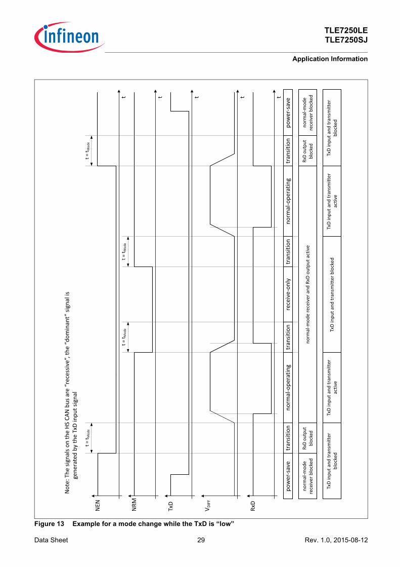
8.3.1 Mode Change while the TxD Signal is “low”The example in Figure 13 shows a mode change to normal-operating mode while the TxD input is logical “low”.The HS CAN signal is “recessive”, assuming all other HS CAN bus subscribers are also sending a “recessive” bussignal.While the transceiver TLE7250 is in power-save mode, the transmitter and the normal-mode receiver are turnedoff. The TLE7250 drives no signal to the HS CAN bus nor does it receive any signal from the HS CAN bus.Changing the NEN to logical “low” turns the mode of operation to normal-operating mode, while the TxD inputsignal remains logical “low”. The transmitter and the normal-mode receiver remain disabled until the modetransition is completed. In normal-operating mode the transceiver and the normal-mode receiver are active. The“low” signal on the TxD input drives a “dominant” signal to the HS CAN bus and the RxD output pin becomeslogical “low”, following the “dominant” signal on the HS CAN bus.Changing the mode of operation from normal-operating mode to receive-only mode by setting the NRM input pinto “low”, disables the transmitter and the TxD input, but the normal-mode receiver and the RxD output remainactive. The HS CAN bus becomes “recessive” since the transmitter is disabled. The RxD input indicates the“recessive” HS CAN bus signal by a logical “high” output signal (see also the example in Figure 13). Mode changes between the power-save mode on the one side and the normal-operating mode or the receive-onlymode on the other side, disable the transmitter and the normal-mode receiver. No signal can be driven to theHS CAN bus nor can it be received from the HS CAN bus. Mode changes between the normal-operating modeand the receive-only mode disable the transmitter and the normal mode receiver remains active. The HS CANtransceiver TLE7250 monitors the HS CAN bus also during the mode transition from normal-operating mode toreceive-only mode and vice versa.
8.3.2 Mode Change while the Bus Signal is “dominant”The example in Figure 14 shows a mode change while the bus is “dominant” and the TxD input signal is set tological “high”.While the transceiver TLE7250 is in power-save mode, the transmitter and the normal-mode receiver are turnedoff. The TLE7250 drives no signal to the HS CAN bus nor does it receive any signal from the HS CAN bus.Changing the NEN to logical “low” turns the mode of operation to normal-operating mode, while the TxD inputsignal remains logical “high”. The transmitter and the normal-mode receiver remain disabled until the modetransition is completed. In normal-operating mode the transceiver and the receiver are active and therefor the RxDoutput changes to logical “low” indicating the “dominant” signal on the HS CAN bus.Changing the mode of operation from normal-operating mode to receive-only mode by setting the NRM input pinto “low”, disables the transmitter and the TxD input, but the normal-mode receiver and the RxD output remainactive. Since the “dominant” signal on the HS CAN bus is driven by another HS CAN bus subscriber, the busremains “dominant” and the RxD input indicates the “dominant” HS CAN bus signal by a logical “low” output signal(see also the example in Figure 14).
TLE7250LETLE7250SJ
Application Information
Data Sheet 29 Rev. 1.0, 2015-08-12
Figure 13 Example for a mode change while the TxD is “low”
RxD
t
V DIF
F
TxD
NRM
t = t M
ode
tpo
wer
-sav
etr
ansit
ion
tran
sitio
nre
ceiv
e-on
lyno
rmal
-ope
ratin
g
RxD
outp
ut
bloc
ked
norm
al-m
ode
rece
iver
and
RxD
out
put a
ctiv
e
TxD
inpu
t and
tran
smitt
er
activ
eTx
D in
put a
nd tr
ansm
itter
bl
ocke
dTx
D in
put a
nd tr
ansm
itter
blo
cked
Not
e: T
he si
gnal
s on
the
HS C
AN b
us a
re “
rece
ssiv
e”, t
he “
dom
inan
t” si
gnal
is
g
ener
ated
by
the
TxD
inpu
t sig
nal
t
NEN
t = t M
ode
norm
al-m
ode
rece
iver
blo
cked
t = t M
ode
tran
sitio
nno
rmal
-ope
ratin
g
TxD
inpu
t and
tran
smitt
er
activ
e
tran
sitio
npo
wer
-sav
e
RxD
outp
ut
bloc
ked
norm
al-m
ode
rece
iver
blo
cked
TxD
inpu
t and
tran
smitt
er
bloc
ked
tt
t = t M
ode

TLE7250LETLE7250SJ
Application Information
Data Sheet 30 Rev. 1.0, 2015-08-12
Figure 14 Example for a mode change while the HS CAN is “dominant”
RxD
t
V DIF
F
TxD
NRM
t = t M
ode
tpo
wer
-sav
etr
ansit
ion
tran
sitio
nre
ceiv
e-on
lyno
rmal
-ope
ratin
g
RxD
outp
ut
bloc
ked
norm
al-m
ode
rece
iver
and
RxD
out
put a
ctiv
e
TxD
inpu
t and
tran
smitt
er
activ
eTx
D in
put a
nd tr
ansm
itter
bl
ocke
dTx
D in
put a
nd tr
ansm
itter
blo
cked
Not
e: T
he “
dom
inan
t” si
gnal
on
the
HS C
AN b
us is
set b
y an
othe
r HS
CAN
bus
subs
crib
er.
t
NEN
t = t M
ode
norm
al-m
ode
rece
iver
blo
cked
t = t M
ode
tran
sitio
nno
rmal
-ope
ratin
g
TxD
inpu
t and
tran
smitt
er
activ
e
tran
sitio
npo
wer
-sav
e
RxD
outp
ut
bloc
ked
norm
al-m
ode
rece
iver
blo
cked
TxD
inpu
t and
tran
smitt
er
bloc
ked
tt
t = t M
ode

TLE7250LETLE7250SJ
Application Information
Data Sheet 31 Rev. 1.0, 2015-08-12
8.4 Further Application Information
• Please contact us for information regarding the pin FMEA.• Existing application note.• For further information you may visit: http://www.infineon.com/

TLE7250LETLE7250SJ
Package Outline
Data Sheet 32 Rev. 1.0, 2015-08-12
9 Package Outline
Figure 15 PG-TSON-8 (Plastic Thin Small Outline Nonleaded PG-TSON-8-1)
Figure 16 PG-DSO-8 (Plastic Dual Small Outline PG-DSO-8-44)
Green Product (RoHS compliant)To meet the world-wide customer requirements for environmentally friendly products and to be compliant withgovernment regulations the device is available as a green product. Green products are RoHS compliant (i.ePb-free finish on leads and suitable for Pb-free soldering according to IPC/JEDEC J-STD-020).
±0.1
0.4
Pin 1 MarkingPin 1 Marking
PG-TSON-8-1-PO V01
±0.1
0.2
±0.1
0.25
0.81
±0.1
2.4±0.1
0.1 ±0.10.3 ±0.10.38
±0.10.3
±0.10.65
±0.1
3
±0.13 ±0.1
0+0
.05
1±0.
1
0.56
±0.1
1.63
±0.1
1.58
±0.10.05
0.07 MIN.
Z (4:1)
Z
+0.0
60.
19
0.35 x 45˚1)
-0.24
C
8 M
AX
.
0.64
±0.26
±0.25
0.2 8xM C
1.27
+0.10.410.2 M A
-0.06
1.75
MA
X.
(1.4
5)
±0.0
70.
175
B
8xB2)
Index Marking
5-0.21)
41
8 5
A
1) Does not include plastic or metal protrusion of 0.15 max. per side2) Lead width can be 0.61 max. in dambar area
GPS01181
0.1
For further information on alternative packages, please visit our website:http://www.infineon.com/packages. Dimensions in mm

TLE7250LETLE7250SJ
Revision History
Data Sheet 33 Rev. 1.0, 2015-08-12
10 Revision History
Revision Date Changes1.00 2015-08-12 Data Sheet created.

Edition 2015-08-12Published byInfineon Technologies AG81726 Munich, Germany© 2006 Infineon Technologies AGAll Rights Reserved.
Legal DisclaimerThe information given in this document shall in no event be regarded as a guarantee of conditions or characteristics. With respect to any examples or hints given herein, any typical values stated herein and/or any information regarding the application of the device, Infineon Technologies hereby disclaims any and all warranties and liabilities of any kind, including without limitation, warranties of non-infringement of intellectual property rights of any third party.
InformationFor further information on technology, delivery terms and conditions and prices, please contact the nearest Infineon Technologies Office (www.infineon.com).
WarningsDue to technical requirements, components may contain dangerous substances. For information on the types in question, please contact the nearest Infineon Technologies Office.Infineon Technologies components may be used in life-support devices or systems only with the express written approval of Infineon Technologies, if a failure of such components can reasonably be expected to cause the failure of that life-support device or system or to affect the safety or effectiveness of that device or system. Life support devices or systems are intended to be implanted in the human body or to support and/or maintain and sustain and/or protect human life. If they fail, it is reasonable to assume that the health of the user or other persons may be endangered.