Embed Size (px)
Citation preview
Hindawi Publishing CorporationISRN Condensed Matter PhysicsVolume 2013, Article ID 142029, 6 pageshttp://dx.doi.org/10.1155/2013/142029
Research ArticleThickness-Dependent Physical Properties ofCoevaporated Cu4SnS4 Films
V. P. Geetha Vani, M. Vasudeva Reddy, and K. T. Ramakrishna Reddy
Department of Physics, Sri Venkateswara University, Tirupati 517 502, India
Correspondence should be addressed to K. T. Ramakrishna Reddy; [email protected]
Received 17 May 2013; Accepted 17 June 2013
Academic Editors: S. Krukowski, Y. Ohta, T. Prokscha, and S. Wang
Copyright © 2013 V. P. Geetha Vani et al. This is an open access article distributed under the Creative Commons AttributionLicense, which permits unrestricted use, distribution, and reproduction in any medium, provided the original work is properlycited.
Cu4SnS4films of different thicknesses were prepared by thermal coevaporation technique on glass substrates at a constant substrate
temperature of 400∘C. The layer thickness was varied in the range 0.25–1𝜇m. The composition analysis revealed that all theevaporated films were nearly stoichiometric. The XRD patterns indicated the presence of a strong (311) peak as the preferredorientation, following the orthorhombic crystal structure corresponding to Cu
4SnS4films. Raman analysis showed a sharp peak
at 317 cm−1, also related to Cu4SnS4phase. The optical transmittance spectra suggested that the energy band gap decreased from
1.47 eV to 1.21 eV with increase of film thickness. The hot-probe test revealed that the layers had p-type electrical conductivity. Adecrease of electrical resistivity was observed with the rise of film thickness.
1. Introduction
In recent years, extensive efforts have been made in findingnovel and new semiconductors for application in energy con-version using the photovoltaic route. One such new materialsystem is the Cu-Sn-S that contains inexpensive, nontoxic,and earth-abundant elements. This ternary system exhibiteddifferent stable phases such as Cu
2SnS3, Cu2Sn3S7, Cu5Sn2S7,
Cu4SnS4, and Cu
10Sn2S13, that was reported by Wu et al. [1].
All these compounds are represented by the general formulaI-IV-VI. Their optimum optical, thermal, and mechanicalproperties with appropriate energy band gap of these mate-rials have attracted much attention for their applicationsin solar cells, sensor and other optoelectronic devices [2].Cu4SnS4is one such material that had an optimum energy
band gap for solar energy conversion along with suitableproperties [3, 4]. Hence, many researchers have attemptedto grow thin films of this material using a variety of wetchemical methods such as chemical bath deposition [5] andelectrodeposition [6]. However, to our knowledge, there wereno attempts made to form Cu
4SnS4films using physical
methods. Therefore, thermal coevaporation technique hasbeen used in this study for the growth of Cu
4SnS4films. It
is one of the best techniques because of the possibility oflarge-scale production, high quality of the grown layers,
and minimum wastage of components. In previous work, wehave shown that thin films of Cu
4SnS4could be obtained by
coevaporating SnS and CuS powders [7].In general, the physical properties of thin films strongly
depend on the deposition technique and growth parametersas well as the film thickness [8]. Film thickness plays animportant role in controlling the film properties unlike itsbulk counterpart, and all the physical properties of thefilms may oscillate with thickness [9–12]. The influence ofcrystallite size on the physical properties has been of muchinterest in semiconductor devices. The structure and surfacemorphology of the film changes with the increase of filmthickness, which will in turn affect the optical transmittance[13, 14] and electronic properties [15, 16]. Hence, in thepresent work, the influence of film thickness on physi-cal properties of Cu
4SnS4films has been investigated and
reported.
2. Experimental Analysis
Cu4SnS4thin films were prepared by thermal coevaporation
technique using Box-type Hind Hi Vac system (model BC-300). 5N pure CuS and SnS were used as the source materials,

2 ISRN Condensed Matter Physics
and the depositions were carried out under a pressure betterthan 10−5 Torr. In this technique, the distance between thesource and substrate is maintained as 20 cm. The mate-rial is kept in a tantalum boat covered with quartz wool,which is heated by resistive heating process. Ultrasonicallycleaned Corning 7059 glass slides were used as substrates fordepositing Cu
4SnS4films. The films were prepared for dif-
ferent thicknesses that vary in the range 0.25–1 𝜇m, keepingthe substrate temperature at 400∘C. The rate of depositionand thickness of the experimental films were determinedusing the quartz crystal thickness monitor (model QTM-101)placed just below the substrate holder. The as-grown layerswere characterized by studying the composition, structural,optical, and electrical properties. The elemental compositionand surface morphology of Cu
4SnS4films were examined
using scanning electron microscope (SEM) (model: ZeissEVOMA 15) attached to the energy dispersive X-ray analyser(EDAX) system (model: INCA Penta FET X3).The structuralproperties of Cu
4SnS4films were measured using an (model:
Seifert 3003TT) X-ray diffractometer (XRD) with Cu-K𝛼
radiation source (𝜆 = 1.5402 A). Raman analysis was carriedout at room temperature with HORIBA JOBIN YVON(model: Lab Ram HR800) Raman spectrometer. The opticaltransmittance of the films was recorded as a function ofwavelength using Perkin Elmer Lambda-950UV-Vis-NIRspectrophotometer in order to determine the optical bandgap, absorption coefficient, and refractive index. The electri-cal properties of the films were recorded by using hot-probemethod, four-probe method, and Hall effect studies.
3. Results and Discussion
Theas-grownCu4SnS4layers were pinhole free, uniform, and
well adherent to the substrate surface. With the increase offilm thickness, the color of the films was changed from pale-brownish yellow to dark-yellowish brown.
3.1. Compositional Analysis. The composition of the differentelements present in Cu
4SnS4films, grown at a constant sub-
strate temperature, was approximately constant althoughthere is an increase of film thickness (𝑡). Figure 1 shows theEDAX spectrum of a typical Cu
4SnS4film grown with a
thickness of 1 𝜇m. It can be seen from the spectrum that therewere peaks corresponding to Cu, Sn, and S, and no otherimpurities were present. The elemental composition of thelayer evaluated using this spectrumwas Cu = 43.35 at. %, Sn =15.56 at. %, and S = 41.09 at. %.
3.2. Structure and Phase Analysis. X-ray diffraction patternsof Cu
4SnS4thin films formed with different thicknesses are
shown in Figure 2. The as-deposited Cu4SnS4films were
polycrystalline and exhibited different peaks that correspondto the (311), (121), (102), (112), (411), (022), (511), (222), (502),(512), (403), and (503) orientations of the Cu
4SnS4. The
films showed (311) plane as the dominant orientation, and itsintensity increased with the increase of film thickness, whichindicates an improvement in the crystallinity of the layers.The crystal structure was evaluated to be orthorhombic.
0 2 4 6 8 10(keV)
Sn
S
Cu
Figure 1: EDAX spectrum of Cu4SnS4film with a thickness of 1 𝜇m.
20 30 40 50 60
Inte
nsity
(a.u
.)
2𝜃 (degrees)
t = 0.25 𝜇mt = 0.75𝜇mt = 0.5 𝜇mt = 1𝜇m
(112
)
(511
)
(102
)
(411
)
(503
)
(403
)
(502
)(5
12)(222
)(0
22)
(121
)(3
11)
Figure 2: XRD spectra of Cu4SnS4films prepared at a substrate
temperature of 400∘C.
Nair et al. [17] also observed a similar behavior with the (311)plane as preferred orientation in Cu
4SnS4films formed by
heating SnS-CuS layers grown by chemical bath depositionmethod.
The lattice parameters corresponding to orthorhombiccrystal structure were calculated using the relation
1
𝑑2=ℎ2
𝑎2+𝑘2
𝑏2+𝑙2
𝑐2, (1)
where 𝑑 is the interplanar distance and (ℎ 𝑘 𝑙) are the Millerindices. The evaluated lattice parameters were 𝑎 = 13.52 A,𝑏 = 7.67 A, and 𝑐 = 6.43 A. The change in lattice parameters
ISRN Condensed Matter Physics 3
𝑎, 𝑏, and 𝑐 with increase of film thickness was found tobe marginal. The evaluated lattice parameters are in closeagreement with the standard JCPDS data file (Card no. 29-0584). The crystallite size, 𝐷, of the as-deposited layers wasevaluated using the Debye-Scherrer formula [18] given by
𝐷 =0.94𝜆
𝛽 cos 𝜃, (2)
where 𝛽 is the full width at half maximum of the (311) peak, 𝜃is the diffraction angle, and 𝜆 is the X-ray wavelength. Thecrystallite size of the films increased from 39 nm to 76 nmwith the increase of film thickness. The increase in crystallitesize might be interpreted in terms of columnar grain growthin the film structure. The observed less grain size at lowerthicknesses might be due to the strong interaction betweenthe substrate and vapour atoms, which restricts the mobilityof ad-atoms.The improvement in the crystallinity of Cu
4SnS4
layers can provide activation energy for the adsorbed atomsto occupy the minimum energy positions, enhancing therecrystallization due to the coalescence of the islands byincreasing the volume and surface diffusions.
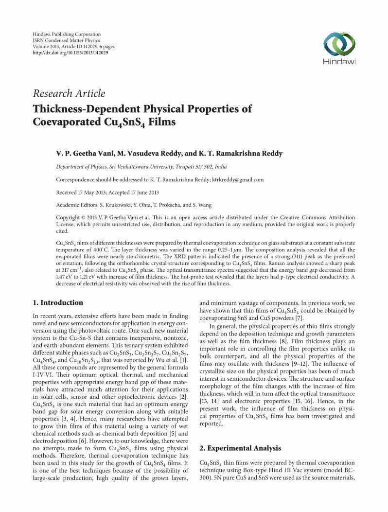
3.3. Raman Analysis. The Raman spectroscopy measure-ments were conducted on the as-grown Cu
4SnS4films in the
wavenumber range 100–600 cm−1 as shown in Figure 3. Fromthe Raman spectra, only one characteristic Raman line couldbe observed at 317 cm−1 for all thicknesses. This vibrationalmode is not related to any other binary or ternary phases ofCu-Sn-S such as SnS, SnS
2, Sn2S3, CuS, Cu
2S, Cu2SnS3, and
Cu3SnS4and is therefore ascribed due to the contribution of
Cu4SnS4phase as it is also confirmed from the XRD analysis.
It could be seen from the Raman spectra that the intensity ofthe peak increased with the increase of film thickness, whichcould be due to the improvement in the crystallinity of thelayers.
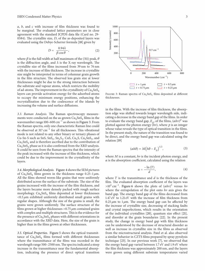
3.4.Morphological Analysis. Figure 4 shows the SEMpicturesof Cu
4SnS4films grown in the thickness range 0.25–1𝜇m.
All the films showed worm-like grains that were uniformlydistributed across the surface of the substrate. The size of thegrains increased with the increase of the film thickness, andthe layers became more densely packed with rough surfacemorphology. Cu
4SnS4films deposited at lower thicknesses
<0.5 𝜇m exhibited uniformly distributed small grains withregular shapes. Although the size of the grains is small, thegrains were grown uniformly. The surface structure of thefilms grown at higher thicknesses >0.75 𝜇m contained grainswith complex andmultiple structures.This is the evidence forthe presence of Cu
4SnS4phases with different orientations in
accordance with the XRD data. Here, the size of the grain ishigher than in the films grown at other thicknesses.
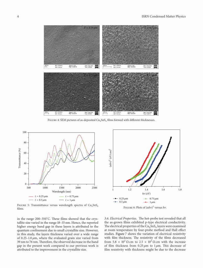
3.5. Optical Properties. Figure 5 shows the optical transmit-tance of Cu
4SnS4films formed with different thicknesses
where the transmittance of the films was recorded in thewavelength range 500–2500 nm.The spectra indicated a steepincrease in the transmittance near the fundamental absorp-tion, indicating the presence of direct optical transition
0 200 400 600 800
200
400
600
800
1000
Inte
nsity
(cou
nts)
t = 0.25 𝜇mt = 0.75𝜇mt = 0.5 𝜇mt = 1𝜇m
317 cm−1
Wavenumber (cm−1)
Figure 3: Raman spectra of Cu4SnS4films deposited at different
thicknesses.
in the films. With the increase of film thickness, the absorp-tion edge was shifted towards longer wavelength side, indi-cating a decrease in the energy band gap of the films. In orderto evaluate the energy band gap, 𝐸
𝑔, of the films, (𝛼ℎ])𝑝 was
plotted against the photon energy (ℎ]), where 𝑝 is an integerwhose value reveals the type of optical transition in the films.In the present study, the nature of the transition was found tobe direct, and the energy band gap was calculated using therelation [19]
(𝛼ℎ𝜗) = 𝑀(ℎ𝜗 − 𝐸𝑔)1/2
, (3)
where𝑀 is a constant, ℎ] is the incident photon energy, and𝛼 is the absorption coefficient, calculated using the relation
𝛼 =− ln (𝑇)𝑑, (4)
where 𝑇 is the transmittance and 𝑑 is the thickness of thefilm. The evaluated absorption coefficient of the layers was>104 cm−1. Figure 6 shows the plots of (𝛼ℎ])2 versus ℎ]where the extrapolation of the plot onto ℎ] axis gives theband gap. The energy band gap of the films decreased from1.47 eV to 1.21 eV with the increase of film thickness from0.25 𝜇m to 1 𝜇m. The energy band gap can be affected bythe increase of crystallite size, decreasing of stacking faultsand crystal imperfections, which results in the orientationof the individual crystallites [20], quantum size effect [21],and disorder at the grain boundaries [22]. In the presentstudy, the change in energy band gap with film thicknesscan be understood by the decrease of structural disorder aswell as increase in crystallite size in the films as observedfrom the microstructural analysis. Patel et al. also observeda similar behavior in CZTS films prepared by spray pyrolysistechnique [23]. In our previous work [7], we observed thatthe energy band gap varied between 1.7 eV and 1.9 eV wherethe film thickness was approximately 200 nm, and the layerswere grown using different substrate temperatures varied
4 ISRN Condensed Matter Physics
T = 0.25 𝜇m T = 0.5 𝜇m
T = 0.75𝜇m T = 1𝜇m
Figure 4: SEM pictures of as-deposited Cu4SnS4films formed with different thicknesses.
t = 0.25 𝜇m t = 0.75𝜇mt = 0.5 𝜇m t = 1𝜇m
500 1000 1500 2000 25000
20
40
60
80
100
Tran
smitt
ance
(%)
Wavelength (nm)
Figure 5: Transmittance versus wavelength spectra of Cu4SnS4
films.
in the range 200–350∘C. These films showed that the crys-tallite size varied in the range 18–35 nm. Hence, the reportedhigher energy band gap in these layers is attributed to thequantum confinement due to small crystallite size. However,in this study, the layers thickness varied over a wide rangeof 0.25–1.0 𝜇m, where the evaluated grain size varied from39 nm to 76 nm.Therefore, the observed decrease in the bandgap in the present work compared to our previous work isattributed to the improvement in the crystallite size.
1 1.2 1.4 1.6 1.8
0.25 𝜇m 0.75𝜇m1𝜇m
h� (eV)
(𝛼h�)2
(eV
/cm
)2
0.5 𝜇m
Figure 6: Plots of (𝛼ℎ])2 versus ℎ].
3.6. Electrical Properties. The hot-probe test revealed that allthe as-grown films exhibited p-type electrical conductivity.The electrical properties of the Cu
4SnS4layers were examined
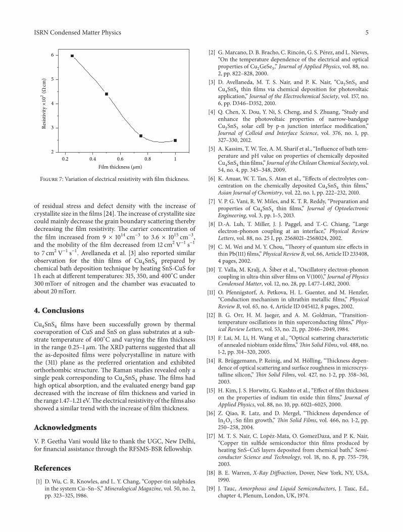
at room temperature by four-probe method and Hall effectstudies. Figure 7 shows the variation of electrical resistivitywith film thickness. The resistivity of the films decreasedfrom 5.8 × 10²Ω cm to 2.5 × 10²Ω cm with the increaseof film thickness from 0.25 𝜇m to 1 𝜇m. This decrease offilm resistivity with thickness might be due to the decrease
ISRN Condensed Matter Physics 5
0.2 0.4 0.6 0.8 12
3
4
5
6
Resis
tivity
×102
(Ωcm
)
Film thickness (𝜇m)
Figure 7: Variation of electrical resistivity with film thickness.
of residual stress and defect density with the increase ofcrystallite size in the films [24].The increase of crystallite sizecould mainly decrease the grain boundary scattering therebydecreasing the film resistivity. The carrier concentration ofthe film increased from 9 × 1014 cm−3 to 3.6 × 1015 cm−3,and the mobility of the film decreased from 12 cm2 V−1 s−1to 7 cm2 V−1 s−1. Avellaneda et al. [3] also reported similarobservation for the thin films of Cu
4SnS4prepared by
chemical bath deposition technique by heating SnS-CuS for1 h each at different temperatures: 315, 350, and 400∘C under300mTorr of nitrogen and the chamber was evacuated toabout 20mTorr.
4. Conclusions
Cu4SnS4films have been successfully grown by thermal
coevaporation of CuS and SnS on glass substrates at a sub-strate temperature of 400∘C and varying the film thicknessin the range 0.25–1𝜇m. The XRD patterns suggested that allthe as-deposited films were polycrystalline in nature withthe (311) plane as the preferred orientation and exhibitedorthorhombic structure. The Raman studies revealed only asingle peak corresponding to Cu
4SnS4phase. The films had
high optical absorption, and the evaluated energy band gapdecreased with the increase of film thickness and varied inthe range 1.47–1.21 eV.The electrical resistivity of the films alsoshowed a similar trend with the increase of film thickness.
Acknowledgments
V. P. Geetha Vani would like to thank the UGC, New Delhi,for financial assistance through the RFSMS-BSR fellowship.
References
[1] D. Wu, C. R. Knowles, and L. Y. Chang, “Copper-tin sulphidesin the system Cu–Sn–S,”Mineralogical Magazine, vol. 50, no. 2,pp. 323–325, 1986.
[2] G.Marcano, D. B. Bracho, C. Rincon, G. S. Perez, and L. Nieves,“On the temperature dependence of the electrical and opticalproperties of Cu
2GeSe3,” Journal of Applied Physics, vol. 88, no.
2, pp. 822–828, 2000.[3] D. Avellaneda, M. T. S. Nair, and P. K. Nair, “Cu
2SnS3and
Cu4SnS4thin films via chemical deposition for photovoltaic
application,” Journal of the Electrochemical Society, vol. 157, no.6, pp. D346–D352, 2010.
[4] Q. Chen, X. Dou, Y. Ni, S. Cheng, and S. Zhuang, “Study andenhance the photovoltaic properties of narrow-bandgapCu2SnS3solar cell by p-n junction interface modification,”
Journal of Colloid and Interface Science, vol. 376, no. 1, pp.327–330, 2012.
[5] A. Kassim, T. W. Tee, A. M. Sharif et al., “Influence of bath tem-perature and pH value on properties of chemically depositedCu4SnS4thin films,” Journal of the Chilean Chemical Society, vol.
54, no. 4, pp. 345–348, 2009.[6] K. Anuar, W. T. Tan, S. Atan et al., “Effects of electrolytes con-
centration on the chemically deposited Cu4SnS4thin films,”
Asian Journal of Chemistry, vol. 22, no. 1, pp. 222–232, 2010.[7] V. P. G. Vani, R. W. Miles, and K. T. R. Reddy, “Preparation and
properties of Cu4SnS4thin films,” Journal of Optoelectronic
Engineering, vol. 3, pp. 1–5, 2013.[8] D.-A. Luh, T. Miller, J. J. Paggel, and T.-C. Chiang, “Large
electron-phonon coupling at an interface,” Physical ReviewLetters, vol. 88, no. 25 I, pp. 2568021–2568024, 2002.
[9] C. M. Wei and M. Y. Chou, “Theory of quantum size effects inthin Pb(111) films,” Physical Review B, vol. 66, Article ID 233408,4 pages, 2002.
[10] T. Valla, M. Kralj, A. Siber et al., “Oscillatory electron-phononcoupling in ultra-thin silver films on V(100),” Journal of PhysicsCondensed Matter, vol. 12, no. 28, pp. L477–L482, 2000.
[11] O. Pfennigstorf, A. Petkova, H. L. Guenter, and M. Henzler,“Conduction mechanism in ultrathin metallic films,” PhysicalReview B, vol. 65, no. 4, Article ID 045412, 8 pages, 2002.
[12] B. G. Orr, H. M. Jaeger, and A. M. Goldman, “Transition-temperature oscillations in thin superconducting films,” Phys-ical Review Letters, vol. 53, no. 21, pp. 2046–2049, 1984.
[13] F. Lai, M. Li, H. Wang et al., “Optical scattering characteristicof annealed niobium oxide films,”Thin Solid Films, vol. 488, no.1-2, pp. 314–320, 2005.
[14] R. Bruggemann, P. Reinig, and M. Holling, “Thickness depen-dence of optical scattering and surface roughness in microcrys-talline silicon,” Thin Solid Films, vol. 427, no. 1-2, pp. 358–361,2003.
[15] H. Kim, J. S. Horwitz, G. Kushto et al., “Effect of film thicknesson the properties of indium tin oxide thin films,” Journal ofApplied Physics, vol. 88, no. 10, pp. 6021–6025, 2000.
[16] Z. Qiao, R. Latz, and D. Mergel, “Thickness dependence ofIn2O3: Sn film growth,” Thin Solid Films, vol. 466, no. 1-2, pp.
250–258, 2004.[17] M. T. S. Nair, C. Lopez-Mata, O. GomezDaza, and P. K. Nair,
“Copper tin sulfide semiconductor thin films produced byheating SnS–CuS layers deposited from chemical bath,” Semi-conductor Science and Technology, vol. 18, no. 8, pp. 755–759,2003.
[18] B. E. Warren, X-Ray Diffraction, Dover, New York, NY, USA,1990.
[19] J. Tauc, Amorphous and Liquid Semiconductors, J. Tauc, Ed.,chapter 4, Plenum, London, UK, 1974.
6 ISRN Condensed Matter Physics
[20] C. D. Lokhande, A. U. Ubale, and P. S. Patil, “Thickness depen-dent properties of chemically deposited Bi
2S3thin films,” Thin
Solid Films, vol. 302, no. 1-2, pp. 1–4, 1997.[21] S. Ilican, Y. Caglar, and M. Caglar, “Preparation and charac-
terization of ZnO thin films deposited by sol-gel spin coatingmethod,” Journal of Optoelectronics and Advanced Materials,vol. 10, no. 10, pp. 2578–2583, 2008.
[22] N. Kumar, U. Parihar, R. Kumar, K. J. Patel, C. J. Panchal, andN. Padha, “Effect of film thickness on optical properties of tinselenide thin films prepared by thermal evaporation for photo-voltaic applications,” American Journal of Materials Science, vol.2, pp. 41–45, 2012.
[23] M. Patel, I. Mukhopadhyay, and A. Ray, “Structural, optical andelectrical properties of spray-deposited CZTS thin films undera non-equilibrium growth condition,” Journal of Physics D, vol.45, Article ID 445103, 10 pages, 2012.
[24] K. L. Chopra, Thin Film Phenomena, McGraw-Hill, New York,NY, USA, 1969.

Submit your manuscripts athttp://www.hindawi.com
Hindawi Publishing Corporationhttp://www.hindawi.com Volume 2014
High Energy PhysicsAdvances in
The Scientific World JournalHindawi Publishing Corporation http://www.hindawi.com Volume 2014
Hindawi Publishing Corporationhttp://www.hindawi.com Volume 2014
FluidsJournal of
Atomic and Molecular Physics
Journal of
Hindawi Publishing Corporationhttp://www.hindawi.com Volume 2014
Hindawi Publishing Corporationhttp://www.hindawi.com Volume 2014
Advances in Condensed Matter Physics
OpticsInternational Journal of
Hindawi Publishing Corporationhttp://www.hindawi.com Volume 2014
Hindawi Publishing Corporationhttp://www.hindawi.com Volume 2014
Advances in
Astronomy
International Journal of
Hindawi Publishing Corporationhttp://www.hindawi.com Volume 2014
Superconductivity
Hindawi Publishing Corporationhttp://www.hindawi.com Volume 2014
Statistical MechanicsInternational Journal of
Hindawi Publishing Corporationhttp://www.hindawi.com Volume 2014
GravityJournal of
Hindawi Publishing Corporationhttp://www.hindawi.com Volume 2014
AstrophysicsJournal of
Hindawi Publishing Corporationhttp://www.hindawi.com Volume 2014
Physics Research International
Hindawi Publishing Corporationhttp://www.hindawi.com Volume 2014
Solid State PhysicsJournal of
Computational Methods in Physics
Journal of
Hindawi Publishing Corporationhttp://www.hindawi.com Volume 2014
Hindawi Publishing Corporationhttp://www.hindawi.com Volume 2014
Soft MatterJournal of
Hindawi Publishing Corporationhttp://www.hindawi.com
AerodynamicsJournal of
Volume 2014
Hindawi Publishing Corporationhttp://www.hindawi.com Volume 2014
PhotonicsJournal of
Hindawi Publishing Corporationhttp://www.hindawi.com Volume 2014
Journal of
Biophysics
Hindawi Publishing Corporationhttp://www.hindawi.com Volume 2014
ThermodynamicsJournal of


![LED???~???????? ?^?? 20140603 [???e????] Application_ENG.pdf · Thermal, EMMI/InGaAs, OBIRCH Texturing (Surface Morphology) Optical profiler, SEM, TEM Film Type and Thickness Measurement](https://img.dokumen.tips/doc/110x75/60077aa4862cf721ed2743b3/led-20140603-e-applicationengpdf-thermal-emmiingaas.jpg)