Embed Size (px)
Citation preview

1
1
J. Lienig, M. Thiele: The Pressing Need for Electromigration-Aware Physical Design, Proc. of ISPD 2018, pp. 144-151,https://doi.org/10.1145/3177540.3177560
1
The Pressing Need for Electromigration-Aware Physical Design
Jens Lienig, Matthias Thiele
Dresden University of Technology
Dresden, Germany
www.ifte.de
2
J. Lienig, M. Thiele: The Pressing Need for Electromigration-Aware Physical Design, Proc. of ISPD 2018, pp. 144-151,https://doi.org/10.1145/3177540.3177560
2
1Current I
Cross-sectional area A
Current densityA
IJ
Please cite as: J. Lienig, M. Thiele "The Pressing Need for Electromigration-Aware Integrated Circuit Design," Proc. of the ACM 2018 Int. Symposium on Physical Design (ISPD'18), Monterey, CA, pp. 144-151, March 2018.https://doi.org/10.1145/3177540.3177560

2
3
J. Lienig, M. Thiele: The Pressing Need for Electromigration-Aware Physical Design, Proc. of ISPD 2018, pp. 144-151,https://doi.org/10.1145/3177540.3177560
3
4
J. Lienig, M. Thiele: The Pressing Need for Electromigration-Aware Physical Design, Proc. of ISPD 2018, pp. 144-151,https://doi.org/10.1145/3177540.3177560
4
Interconnect is EM-affected
Manufacturable EM-robust solutions are NOT known
3
5
J. Lienig, M. Thiele: The Pressing Need for Electromigration-Aware Physical Design, Proc. of ISPD 2018, pp. 144-151,https://doi.org/10.1145/3177540.3177560
5
Current density needed to drive four inverter gates
16 14 12 10 8 66
5
4
3
2
1
02016 2018 2022 202620242020
Minimum gate length in nm
Year
Current density
in MA/cm2
6
J. Lienig, M. Thiele: The Pressing Need for Electromigration-Aware Physical Design, Proc. of ISPD 2018, pp. 144-151,https://doi.org/10.1145/3177540.3177560
6
Contents
1 Introduction to Electromigration (EM)
2 Mitigating EM in Physical Design – What are Today’s Options?
3 Outlook – What to Do in the “Red Area”?
4 Summary

4
7
J. Lienig, M. Thiele: The Pressing Need for Electromigration-Aware Physical Design, Proc. of ISPD 2018, pp. 144-151,https://doi.org/10.1145/3177540.3177560
7
Electromigration (EM):
Electromigration is the forced movement of metal ions due to an
electric field
Ftotal = Fdirect + Fwind
Direct action of electric field on metal ions
Force on metal ions resulting from momentum transfer from the conduction electrons
Anode+
Cathode-
<<
Introduction: Electromigration
Anode+
Cathode-
E-
-
-
Cu+
8
J. Lienig, M. Thiele: The Pressing Need for Electromigration-Aware Physical Design, Proc. of ISPD 2018, pp. 144-151,https://doi.org/10.1145/3177540.3177560
8
Introduction: Electromigration
Effects of electromigration in metal interconnects:
• Atomic depletion (voids):
Slow reduction in connectivity
Interconnect failure
• Atomic deposition
(hillocks, whiskers):
Short-cuts
Metal atoms (ions) travel towards the positive end of the conductor
while vacancies move towards the negative end
Voids
Hillocks
5
9
J. Lienig, M. Thiele: The Pressing Need for Electromigration-Aware Physical Design, Proc. of ISPD 2018, pp. 144-151,https://doi.org/10.1145/3177540.3177560
9
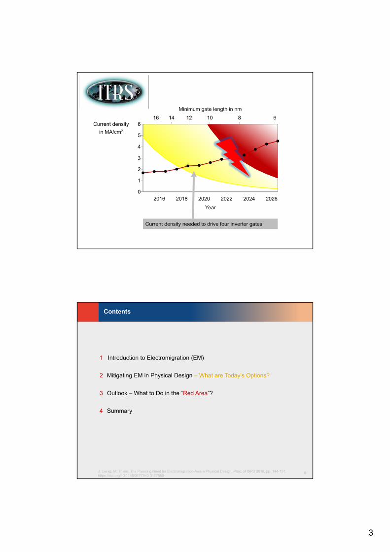
MTF · exp·
Electromigration and Current Density
Black’s Equation:Median time to failure (MTF) of a single segment due to electromigration
Cross-sectional-area-dependent constant
Activation energyfor electromigration
Temperature
Boltzmann constantCurrent density Scaling factor(usually set to 2)
Black, J.R. : “Electromigration - A brief survey and some recent results”; Proc. of IEEE Reliability Physics Symposium, Washington D.C., 1968.
Current density is key to addressing electromigration during physical design
10
J. Lienig, M. Thiele: The Pressing Need for Electromigration-Aware Physical Design, Proc. of ISPD 2018, pp. 144-151,https://doi.org/10.1145/3177540.3177560
10
• Conventional metal wires (house wiring, etc.)
Al 19,100 A/cm2
Cu 30,400 A/cm2
… reaching melting temperature due to Joule heating
Maximum Tolerable Current Densities
• Thin film interconnect on integrated circuits can sustain current densitiesup to 1010 A/cm2 before reaching melting temperature, however, at
Al 200,000 A/cm2
Cu (Jmax(Cu) 5* Jmax(Al) ) 1,000,000 A/cm2
… it reaches its maximum value due to the occurance of electromigration
Melting temperature limits maximum current densities
Electromigration limits maximum current densities

6
11
J. Lienig, M. Thiele: The Pressing Need for Electromigration-Aware Physical Design, Proc. of ISPD 2018, pp. 144-151,https://doi.org/10.1145/3177540.3177560
11
• Rule of Thumb for Copper IC Interconnects
Electromigration to be considered 10,000 - 100,000 A/cm2
Effects visible 500,000 A/cm2
Rapid destruction 30,000,000 A/cm2
(25°C, Source: AMD Saxony)
Electromigration limits maximum current densities
Maximum Tolerable Current Densities
12
J. Lienig, M. Thiele: The Pressing Need for Electromigration-Aware Physical Design, Proc. of ISPD 2018, pp. 144-151,https://doi.org/10.1145/3177540.3177560
12
Contents
1 Introduction to Electromigration (EM)
2 Mitigating EM in Physical Design – What are Today’s Options?
3 Outlook – What to Do in the “Red Area”?
4 Summary

7
13
J. Lienig, M. Thiele: The Pressing Need for Electromigration-Aware Physical Design, Proc. of ISPD 2018, pp. 144-151,https://doi.org/10.1145/3177540.3177560
13
Wire widths, double/multiple vias
Surface coating, metal capping
Wire widths
Segment lengths
Via-above/via-below configurations
(Metal-via) overlaps, multiple vias
Frequency of the current
Local current density
Surface diffusion in Cu
Bamboo effect
Short-length effects
Impact of voids
Reservoir effect
Damage-healing (self-healing)effect
Mitigating EM in Physical Design – What are Today’s Options?
14
J. Lienig, M. Thiele: The Pressing Need for Electromigration-Aware Physical Design, Proc. of ISPD 2018, pp. 144-151,https://doi.org/10.1145/3177540.3177560
14
Bamboo Effect
Wire Width w [m]
MTF [h]I = constantT = constant
wMTF_min
w < Grains(Bamboo Wires) w Grains
– +Diffusion
Grain Boundary
w

8
15
J. Lienig, M. Thiele: The Pressing Need for Electromigration-Aware Physical Design, Proc. of ISPD 2018, pp. 144-151,https://doi.org/10.1145/3177540.3177560
15
Bamboo Effect
Wire Width w [m]
MTF [h]I = constantT = constant
wMTF_min
w < Grains(Bamboo Wires) w = Grains
– +Diffusion
Grain Boundary
w
Practical Applications*
w ≤ 850 nm
* Damascene Copper [Ar99]
16
J. Lienig, M. Thiele: The Pressing Need for Electromigration-Aware Physical Design, Proc. of ISPD 2018, pp. 144-151,https://doi.org/10.1145/3177540.3177560
16
Short-Length Effects: (1) Blech Immortality Condition
– +
FN5FN4FN3FN2FN1
Cu+Cu+ Cu+Cu+ Cu+Cu+
Electromigration (EM)
– +
FN5FN4FN3FN2FN1
Cu+Cu+Cu+ Cu+Cu+
Cu+Cu+
Equilibrium between EM and SMif Lsegment < “Blech length”
– +
FN5FN4FN3FN2FN1
Cu+Cu+Cu+ Cu+Cu+Cu+
Stress Migration (SM)
Tensile
Compressive Stress
Tensile
Compressive Stress

9
17
J. Lienig, M. Thiele: The Pressing Need for Electromigration-Aware Physical Design, Proc. of ISPD 2018, pp. 144-151,https://doi.org/10.1145/3177540.3177560
17
Short-Length Effects: (1) Blech Immortality Condition
– +
FN5FN4FN3FN2FN1
Al+Al+ Al+ Al+ Al+Al+
Electromigration (EM)
– +
FN5FN4FN3FN2FN1
Al+Al+Al+ Al+Al+
Al+Al+
– +
FN5FN4FN3FN2FN1
Al+Al+Al+ Al+ Al+Al+
Stress Migration (SM)
Equilibrium between EM and SMif Lsegment < “Blech length”
Practical Applications
Lsegment ≤ 5 - 50 µm
18
J. Lienig, M. Thiele: The Pressing Need for Electromigration-Aware Physical Design, Proc. of ISPD 2018, pp. 144-151,https://doi.org/10.1145/3177540.3177560
18
Short-Length Effects: (2) Void Growth Saturation
Metal (Cu)Metallic Barrier (Liner)Dielectric Passivation (Cap Layer)
– +
Void
Cap Layer
Liner Layere-
Electromigration (EM)
Tensile
CompressiveStress

10
19
J. Lienig, M. Thiele: The Pressing Need for Electromigration-Aware Physical Design, Proc. of ISPD 2018, pp. 144-151,https://doi.org/10.1145/3177540.3177560
19
Short-Length Effects: (2) Void Growth Saturation
Metal (Cu)Metallic Barrier (Liner)Dielectric Passivation (Cap Layer)
Tensile
CompressiveStress
Void growth saturation due to mechanical stress buildup if JLsegment < JLsaturation
– +
Void
e-
Electromigration (EM)Stress Migration (SM)
20
J. Lienig, M. Thiele: The Pressing Need for Electromigration-Aware Physical Design, Proc. of ISPD 2018, pp. 144-151,https://doi.org/10.1145/3177540.3177560
20
Void growth saturation due to mechanical stress buildup if JLsegment < JLsaturation
Short-Length Effects: (2) Void Growth Saturation
– +
Void
Cap Layer
Liner Layer
Electromigration (EM)Stress Migration (SM)
*J = 5 x 10⁵ A/cm2, [HR03][LE02]
Tensile
CompressiveStress
Practical Applications*
(JL)saturation = 375 A/cm (Cu, low-k) … 3,700 A/cm (Cu, high-k)
L ≤ 7.5 µm … 74 µm

11
21
J. Lienig, M. Thiele: The Pressing Need for Electromigration-Aware Physical Design, Proc. of ISPD 2018, pp. 144-151,https://doi.org/10.1145/3177540.3177560
21
Via-below and Via-above Configuration
– +
Void
Cap Layer
Liner Layere-
Metal (Cu)Metallic Barrier (Liner)Dielectric Passivation (Cap Layer)
– +
Void
e-
Via-below
Via-above
22
J. Lienig, M. Thiele: The Pressing Need for Electromigration-Aware Physical Design, Proc. of ISPD 2018, pp. 144-151,https://doi.org/10.1145/3177540.3177560
22
Via-below and Via-above Configuration
– +e-
(JL) = 1,500 A/cm
L ≤ 30 µm
Practical Applications*
– +
e-
Via-below
Via-above
(JL) = 3,700 A/cm
L ≤ 74 µm
*J = 5 x 10⁵ A/cm2, Cu, high-k,[LE02] [HR02]
12
23
J. Lienig, M. Thiele: The Pressing Need for Electromigration-Aware Physical Design, Proc. of ISPD 2018, pp. 144-151,https://doi.org/10.1145/3177540.3177560
23
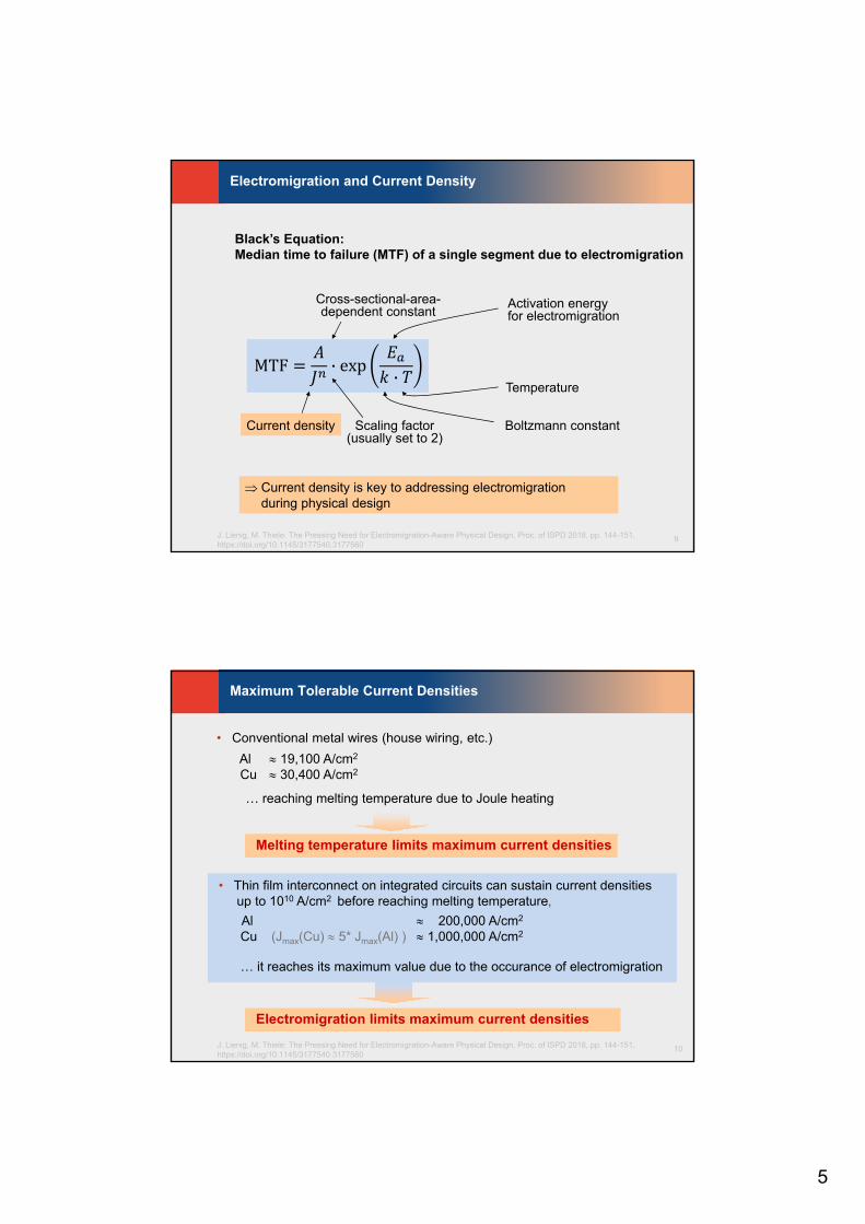
Reservoir Effect
Material sinkMaterial source
e-e-Metal 2
Metal 1
Via
– +
e-
Void nucleation
Tim
e
Open circuit
e-
e-
24
J. Lienig, M. Thiele: The Pressing Need for Electromigration-Aware Physical Design, Proc. of ISPD 2018, pp. 144-151,https://doi.org/10.1145/3177540.3177560
24
Reservoir Effect
Material sinkMaterial source
Tim
e
e-e-
e-
e-
Metal 2
Metal 1
Via

13
25
J. Lienig, M. Thiele: The Pressing Need for Electromigration-Aware Physical Design, Proc. of ISPD 2018, pp. 144-151,https://doi.org/10.1145/3177540.3177560
25
Double/Multiple Vias
http://www.ee.ncu.edu.tw/~
cad_
cont
est/
Pro
blem
s/95
/PB
2/20
07_B
2.pd
f
Metal 1
Met
al2
Metal 1
Met
al 2 Overstrained
via
max
minCur
rent
dens
ityJ
26
J. Lienig, M. Thiele: The Pressing Need for Electromigration-Aware Physical Design, Proc. of ISPD 2018, pp. 144-151,https://doi.org/10.1145/3177540.3177560
26
Self-Healing Effect
Tao, J.; Cheung, N.; Hu, C.: Metal Electromigration Damage Healing under Bidirectional Current Stress, Electron Device Letters, IEEE, vol. 14, no. 12, 554–556, 1993
Frequency in Hz
Lifetime10 Hz … 10 kHz
500-fold increase in MTF
for Cu interconnectMTF ACMTF DC
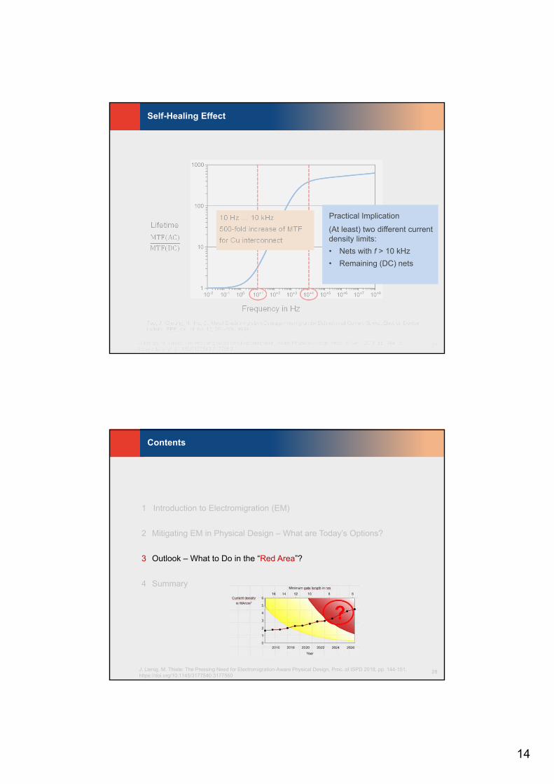
14
27
J. Lienig, M. Thiele: The Pressing Need for Electromigration-Aware Physical Design, Proc. of ISPD 2018, pp. 144-151,https://doi.org/10.1145/3177540.3177560
27
MTF ACMTF DC
Self-Healing Effect
Tao, J.; Cheung, N.; Hu, C.: Metal Electromigration Damage Healing under Bidirectional Current Stress, Electron Device Letters, IEEE, vol. 14, no. 12, 554–556, 1993
Frequency in Hz
Lifetime10 Hz … 10 kHz
500-fold increase of MTF
for Cu interconnect
Practical Implication
(At least) two different currentdensity limits:
• Nets with f > 10 kHz
• Remaining (DC) nets
28
J. Lienig, M. Thiele: The Pressing Need for Electromigration-Aware Physical Design, Proc. of ISPD 2018, pp. 144-151,https://doi.org/10.1145/3177540.3177560
28
Contents
1 Introduction to Electromigration (EM)
2 Mitigating EM in Physical Design – What are Today’s Options?
3 Outlook – What to Do in the “Red Area”?
4 Summary

15
30
J. Lienig, M. Thiele: The Pressing Need for Electromigration-Aware Physical Design, Proc. of ISPD 2018, pp. 144-151,https://doi.org/10.1145/3177540.3177560
30
Outlook: Critical Length Effect
Le
ngt
hin
µm
0,0
0,5
1,0
1,5
2,0
2016 2020 2024 2028
Year
Actual meansegment lengths
Values from ITRS 2014, calculated for respective technology node
Blech lengths increasingly exceeded
Utilization of reservoir effect(multipe/double vias, etc.)
Critical lengthlimits
31
J. Lienig, M. Thiele: The Pressing Need for Electromigration-Aware Physical Design, Proc. of ISPD 2018, pp. 144-151,https://doi.org/10.1145/3177540.3177560
31
Outlook: EM-Robust Layout Elements
Today Future
Currentdensity
“Forbidden elements”
EM-robust layout elements
New constraint in physical design
16
32
J. Lienig, M. Thiele: The Pressing Need for Electromigration-Aware Physical Design, Proc. of ISPD 2018, pp. 144-151,https://doi.org/10.1145/3177540.3177560
32
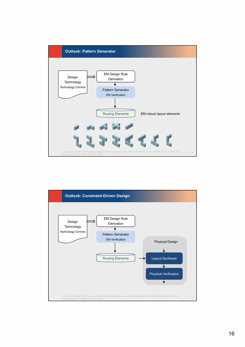
Outlook: Pattern Generator
Pattern Generator
EM Verification
EM Design Rule
Derivation
Routing Elements EM-robust layout elements
Design
Technology
Technology Corners
33
J. Lienig, M. Thiele: The Pressing Need for Electromigration-Aware Physical Design, Proc. of ISPD 2018, pp. 144-151,https://doi.org/10.1145/3177540.3177560
33
Outlook: Constraint-Driven Design
Layout Synthesis
Physical Verification
Physical Design
Design
Technology
Technology CornersPattern Generator
EM Verification
EM Design Rule
Derivation
Routing Elements
17
34
J. Lienig, M. Thiele: The Pressing Need for Electromigration-Aware Physical Design, Proc. of ISPD 2018, pp. 144-151,https://doi.org/10.1145/3177540.3177560
34
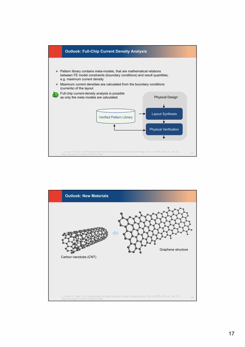
Outlook: Full-Chip Current Density Analysis
Verified Pattern LibraryLayout Synthesis
Physical Verification
Physical Design
Pattern library contains meta-models, that are mathematical relationsbetween FE model constraints (boundary conditions) and result quantities,e.g. maximum current density
Maximum current densities are calculated from the boundary conditions(currents) of the layout
Full-chip current-density analysis is possibleas only the meta models are calculated
35
J. Lienig, M. Thiele: The Pressing Need for Electromigration-Aware Physical Design, Proc. of ISPD 2018, pp. 144-151,https://doi.org/10.1145/3177540.3177560
35
Outlook: New Materials
Graphene structure
Carbon nanotube (CNT)

18
36
J. Lienig, M. Thiele: The Pressing Need for Electromigration-Aware Physical Design, Proc. of ISPD 2018, pp. 144-151,https://doi.org/10.1145/3177540.3177560
36
Outlook: New Materials
CuSingle-wall
CNTsMulti-wall CNTs
Cu-CNT Composites
Maximum current density (A/cm2)
1∙106 > 1∙109 > 1∙109 > 6∙108
Thermal conductivity @300K (W/m∙K)
385 3,000-10,000 3,000 ~ 800
Sources: Fraunhofer IPMS, Dresden, Germany, H2020 CONNECT Project, and A. Todri-Sanial et al., “A Survey of Carbon Nanotube Interconnects for Energy Efficient Integrated Circuits”, IEEE Circuits and Systems Magazine, no. 2, pp. 47–62, 2017.
38
J. Lienig, M. Thiele: The Pressing Need for Electromigration-Aware Physical Design, Proc. of ISPD 2018, pp. 144-151,https://doi.org/10.1145/3177540.3177560
38
Summary
Restricting physical design to EM-robust structures can provide relieffrom severe reliability constraints in future technologies
Need to increase current density limits by putting in placeEM-inhibiting measures, such as short-length and reservoir effects
Future design flows: using the dependence between current density limitsand the specific layout geometry
Pattern generator: generates EM-robust layout configurationsbased on the technological parameters of the specific design
Utilizing these layout configurations, design tools can significantlyimprove the EM robustness of the circuit
Electromigration is fast becoming a physical design problemdue to increased current densities driven by IC down-scaling
Please cite as: J. Lienig, M. Thiele "The Pressing Need for Electromigration-Aware Integrated Circuit Design," Proc. of the ACM 2018 Int. Symposium on Physical Design (ISPD'18), Monterey, CA, pp. 144-151, March 2018.https://doi.org/10.1145/3177540.3177560