Embed Size (px)
Citation preview
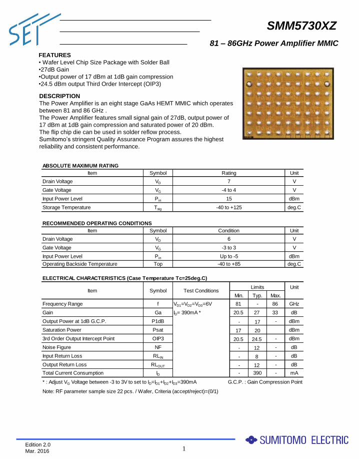
81 – 86GHz Power Amplifier MMIC
SMM5730XZ
1 Edition 2.0
Mar. 2016
ABSOLUTE MAXIMUM RATING
Item Symbol Unit
Drain Voltage VD V
Gate Voltage VG V
Input Power Level Pin dBm
Storage Temperature Tstg deg.C
RECOMMENDED OPERATING CONDITIONS
Item Symbol Unit
Drain Voltage VD V
Gate Voltage VG V
Input Power Level Pin dBm
Operating Backside Temperature Top deg.C
ELECTRICAL CHARACTERISTICS (Case Temperature Tc=25deg.C)
Unit
Min. Typ. Max.
Frequency Range f VD1=VD2=VD3=6V 81 - 86 GHz
Gain Ga ID= 390mA * 20.5 27 33 dB
Output Power at 1dB G.C.P. P1dB - 17 - dBm
Saturation Power Psat 17 20 dBm
3rd Order Output Intercept Point OIP3 20.5 24.5 - dBm
Noise Figure NF - 12 - dB
Input Return Loss RLIN - 8 - dB
Output Return Loss RLOUT - 12 - dB
Total Current Consumption ID - 390 - mA
* : Adjust VG Voltage between -3 to 3V to set to ID=ID1+ID2+ID3=390mA G.C.P. : Gain Compression Point
Note: RF parameter sample size 22 pcs. / Wafer, Criteria (accept/reject)=(0/1)
-40 to +85
Rating
7
-4 to 4
15
-40 to +125
Condition
6
-3 to 3
Up to -5
Item Symbol Test ConditionsLimits
FEATURES
• Wafer Level Chip Size Package with Solder Ball
•27dB Gain
•Output power of 17 dBm at 1dB gain compression
•24.5 dBm output Third Order Intercept (OIP3)
DESCRIPTION
The Power Amplifier is an eight stage GaAs HEMT MMIC which operates
between 81 and 86 GHz .
The Power Amplifier features small signal gain of 27dB, output power of
17 dBm at 1dB gain compression and saturated power of 20 dBm.
The flip chip die can be used in solder reflow process.
Sumitomo’s stringent Quality Assurance Program assures the highest
reliability and consistent performance.
81 – 86GHz Power Amplifier MMIC
SMM5730XZ
2 Edition 2.0
Mar. 2016
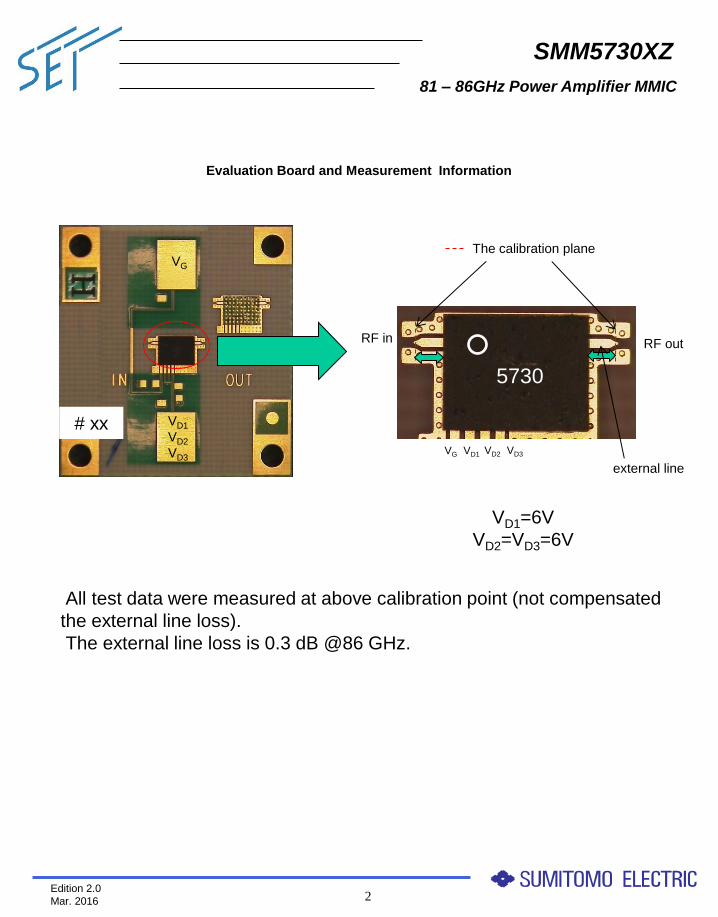
VD1=6V
VD2=VD3=6V
# xx
Evaluation Board and Measurement Information
RF in RF out
VD1 VD2 VD3
The calibration plane
VD1
VD2
VD3
external line
VG
VG
5730
All test data were measured at above calibration point (not compensated
the external line loss).
The external line loss is 0.3 dB @86 GHz.

81 – 86GHz Power Amplifier MMIC
SMM5730XZ
3 Edition 2.0
Mar. 2016
VD1=VD2=VD3=6V
ID=390 mA
Linear Gain and Return vs. Frequency
Linear Gain vs. ID
VD1=VD2=VD3=6V
81 – 86GHz Power Amplifier MMIC
SMM5730XZ
4 Edition 2.0
Mar. 2016
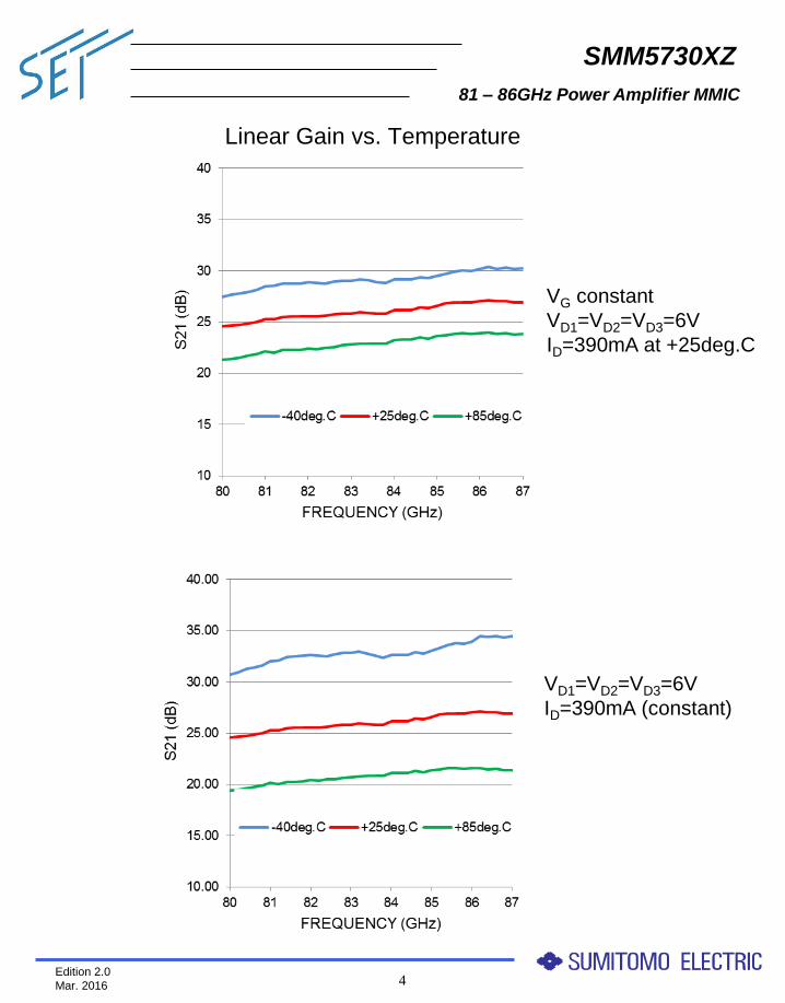
Linear Gain vs. Temperature
VG constant
VD1=VD2=VD3=6V
ID=390mA at +25deg.C
VD1=VD2=VD3=6V
ID=390mA (constant)
81 – 86GHz Power Amplifier MMIC
SMM5730XZ
5 Edition 2.0
Mar. 2016
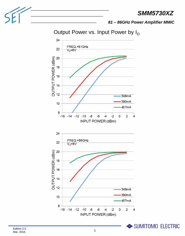
Output Power vs. Input Power by ID
81 – 86GHz Power Amplifier MMIC
SMM5730XZ
6 Edition 2.0
Mar. 2016
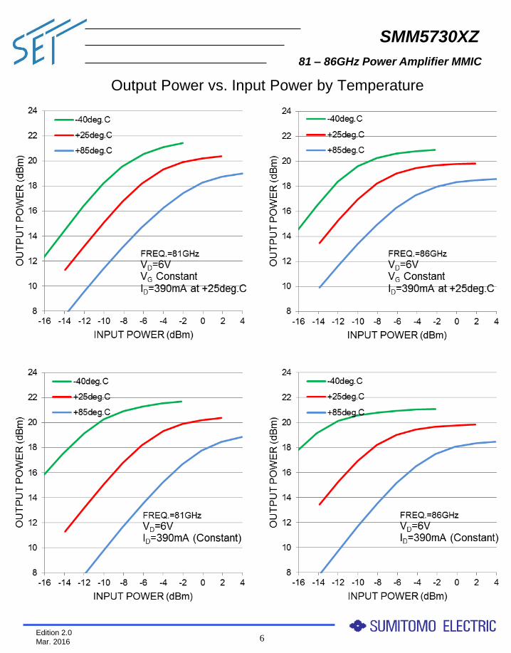
Output Power vs. Input Power by Temperature

81 – 86GHz Power Amplifier MMIC
SMM5730XZ
7 Edition 2.0
Mar. 2016
IM3 vs. Output Power by ID
81 – 86GHz Power Amplifier MMIC
SMM5730XZ
8 Edition 2.0
Mar. 2016
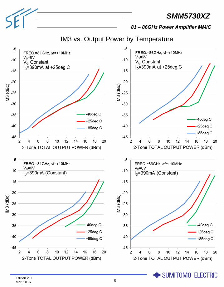
IM3 vs. Output Power by Temperature
81 – 86GHz Power Amplifier MMIC
SMM5730XZ
9 Edition 2.0
Mar. 2016
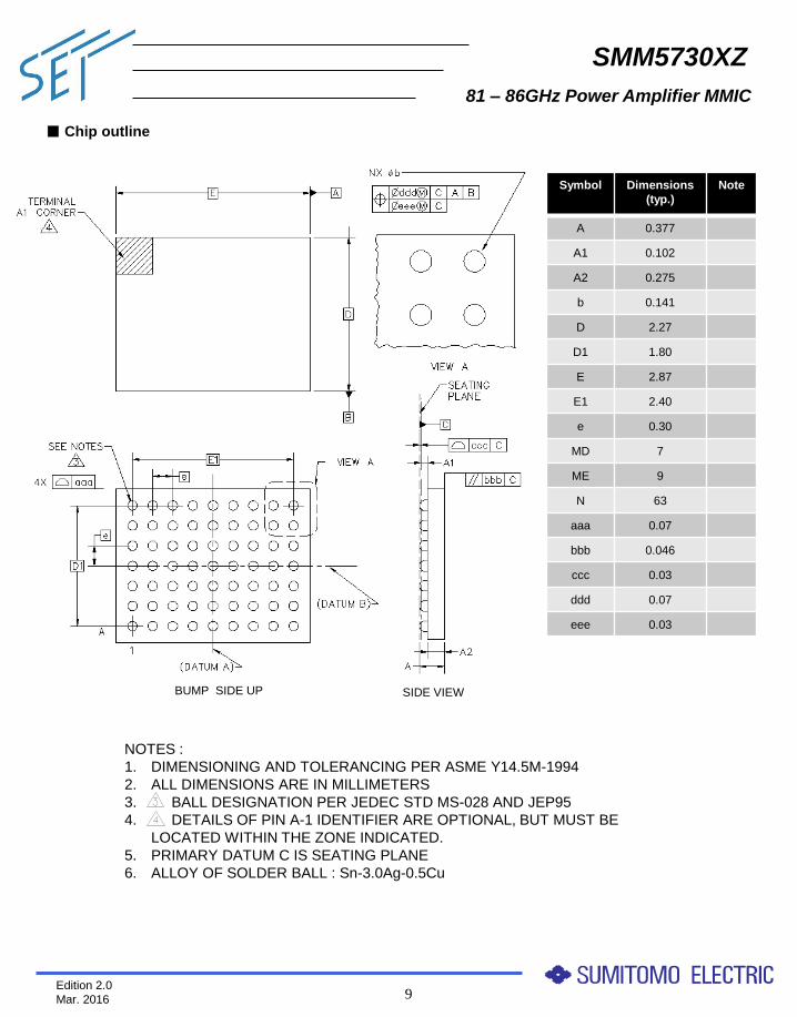
■ Chip outline
Symbol Dimensions
(typ.)
Note
A 0.377
A1 0.102
A2 0.275
b 0.141
D 2.27
D1 1.80
E 2.87
E1 2.40
e 0.30
MD 7
ME 9
N 63
aaa 0.07
bbb 0.046
ccc 0.03
ddd 0.07
eee 0.03
NOTES :
1. DIMENSIONING AND TOLERANCING PER ASME Y14.5M-1994
2. ALL DIMENSIONS ARE IN MILLIMETERS
3. BALL DESIGNATION PER JEDEC STD MS-028 AND JEP95
4. DETAILS OF PIN A-1 IDENTIFIER ARE OPTIONAL, BUT MUST BE
LOCATED WITHIN THE ZONE INDICATED.
5. PRIMARY DATUM C IS SEATING PLANE
6. ALLOY OF SOLDER BALL : Sn-3.0Ag-0.5Cu
BUMP SIDE UP SIDE VIEW
81 – 86GHz Power Amplifier MMIC
SMM5730XZ
10 Edition 2.0
Mar. 2016
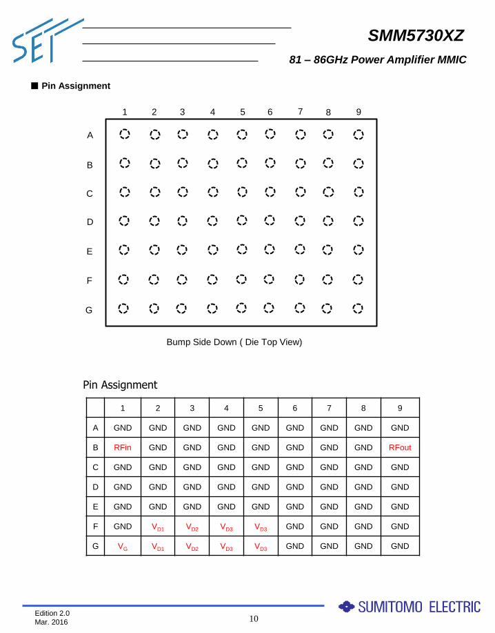
■ Pin Assignment
Bump Side Down ( Die Top View)
A
B
C
D
E
1 2 3 4 5 6 7
F
G
8 9
Pin Assignment
1 2 3 4 5 6 7 8 9
A GND GND GND GND GND GND GND GND GND
B RFin GND GND GND GND GND GND GND RFout
C GND GND GND GND GND GND GND GND GND
D GND GND GND GND GND GND GND GND GND
E GND GND GND GND GND GND GND GND GND
F GND VD1 VD2 VD3 VD3 GND GND GND GND
G VG VD1 VD2 VD3 VD3 GND GND GND GND
81 – 86GHz Power Amplifier MMIC
SMM5730XZ
11 Edition 2.0
Mar. 2016
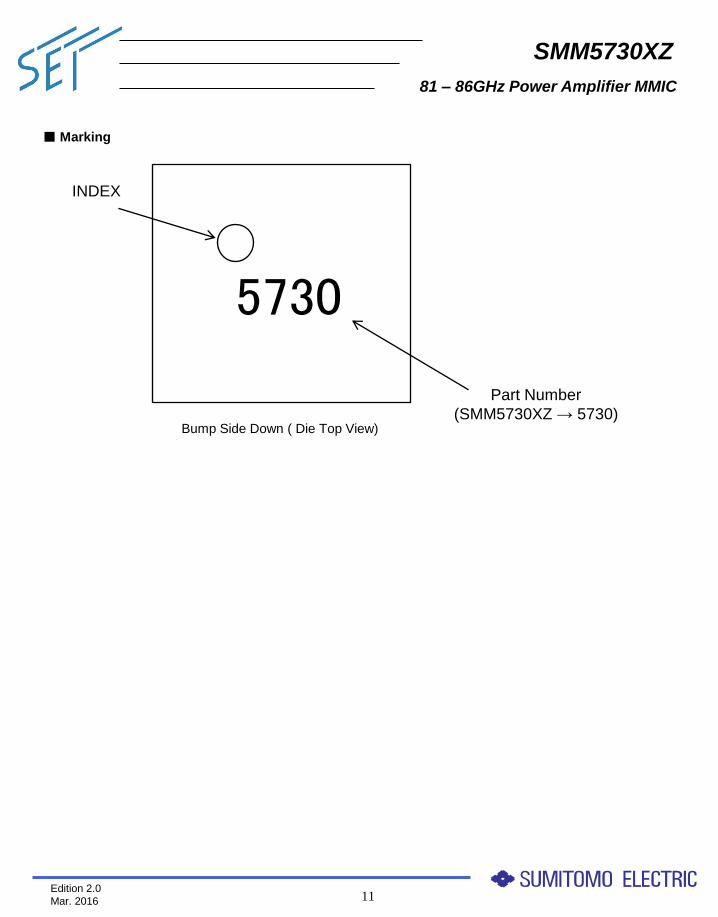
■ Marking
5730
Part Number
(SMM5730XZ → 5730)
INDEX
Bump Side Down ( Die Top View)
81 – 86GHz Power Amplifier MMIC
SMM5730XZ
12 Edition 2.0
Mar. 2016
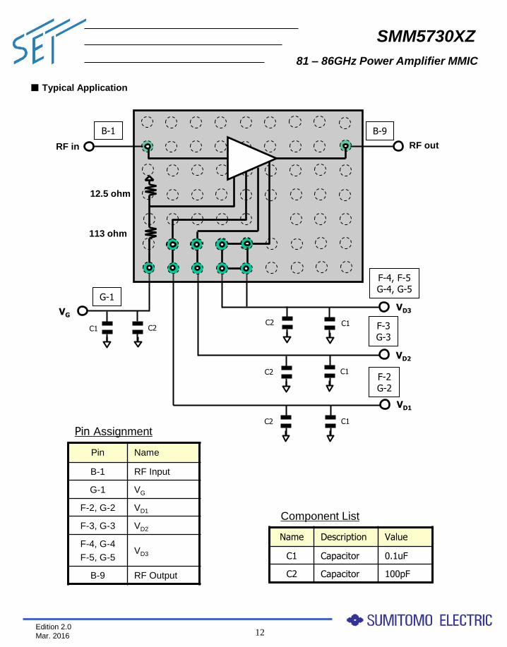
■ Typical Application
Component List
Name Description Value
C1 Capacitor 0.1uF
C2 Capacitor 100pF
Pin Name
B-1 RF Input
G-1 VG
F-2, G-2 VD1
F-3, G-3 VD2
F-4, G-4
F-5, G-5 VD3
B-9 RF Output
Pin Assignment
RF in
VD3
C1
VD2
C1
VD1
C1
VG
C1
RF out
12.5 ohm
113 ohm
C2 C2
C2
C2
B-1
G-1
B-9
F-3 G-3
F-2 G-2
F-4, F-5 G-4, G-5

81 – 86GHz Power Amplifier MMIC
SMM5730XZ
13 Edition 2.0
Mar. 2016
Cross Section
Base Metal
Cu:1.0mm
Core Material
Hitachi Chemical Co.
MCL-E-679F:0.10mm
Metal Pattern
Cu/Ni/Au:0.030mm
Resist Pattern
maximum:0.020mm
■ PCB and Solder-resist Pattern
DC(or IF) Probe Pitch 0.30mm
Metal Pattern
Resist Pattern
Ground Via Hole f0.10mm Resist Window
f0.12mm 0.30mm pitch
81 – 86GHz Power Amplifier MMIC
SMM5730XZ
14 Edition 2.0
Mar. 2016
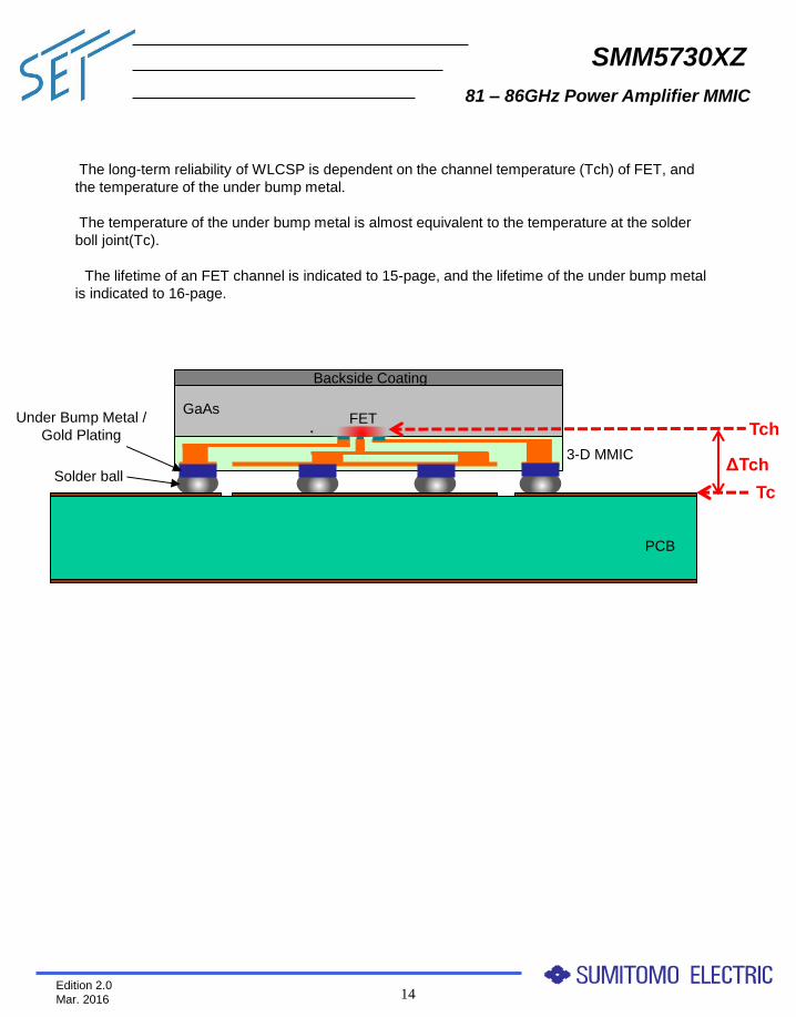
Solder ball
Under Bump Metal /
Gold Plating
GaAs
Backside Coating
FET
3-D MMIC
PCB
Tc
Tch
ΔTch
The long-term reliability of WLCSP is dependent on the channel temperature (Tch) of FET, and
the temperature of the under bump metal.
The temperature of the under bump metal is almost equivalent to the temperature at the solder
boll joint(Tc).
The lifetime of an FET channel is indicated to 15-page, and the lifetime of the under bump metal
is indicated to 16-page.
81 – 86GHz Power Amplifier MMIC
SMM5730XZ
15 Edition 2.0
Mar. 2016
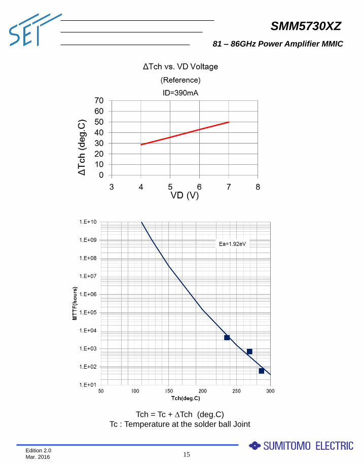
Tch = Tc + DTch (deg.C)
Tc : Temperature at the solder ball Joint

81 – 86GHz Power Amplifier MMIC
SMM5730XZ
16 Edition 2.0
Mar. 2016
The life time of the solder ball joint is dependent on temperature.
Tc : Temperature at the solder ball Joint

81 – 86GHz Power Amplifier MMIC
SMM5730XZ
17 Edition 2.0
Mar. 2016
3.8
3.9
6■ 2-inch Tray Packing (Part No. : SMM5730XZ)

81 – 86GHz Power Amplifier MMIC
SMM5730XZ
18 Edition 2.0
Mar. 2016
■ Tape and Reel Packing (Part No. : SMM5730ZT)
81 – 86GHz Power Amplifier MMIC
SMM5730XZ
19 Edition 2.0
Mar. 2016
■ Assembly Techniques for WLCSP MMICs
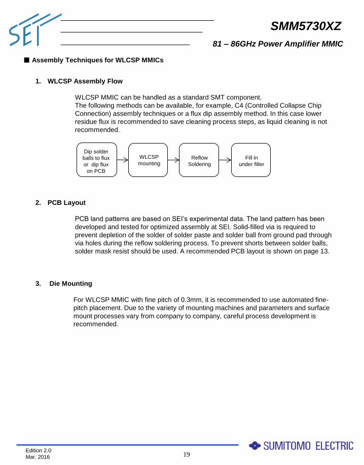
1. WLCSP Assembly Flow
WLCSP MMIC can be handled as a standard SMT component.
The following methods can be available, for example, C4 (Controlled Collapse Chip
Connection) assembly techniques or a flux dip assembly method. In this case lower
residue flux is recommended to save cleaning process steps, as liquid cleaning is not
recommended.
2. PCB Layout
PCB land patterns are based on SEI’s experimental data. The land pattern has been
developed and tested for optimized assembly at SEI. Solid-filled via is required to
prevent depletion of the solder of solder paste and solder ball from ground pad through
via holes during the reflow soldering process. To prevent shorts between solder balls,
solder mask resist should be used. A recommended PCB layout is shown on page 13.
3. Die Mounting
For WLCSP MMIC with fine pitch of 0.3mm, it is recommended to use automated fine-
pitch placement. Due to the variety of mounting machines and parameters and surface
mount processes vary from company to company, careful process development is recommended.
Dip solder
balls to flux
or dip flux
on PCB
WLCSP
mounting Reflow
Soldering
Fill in
under filler
81 – 86GHz Power Amplifier MMIC
SMM5730XZ
20 Edition 2.0
Mar. 2016
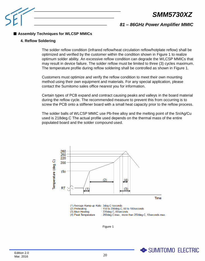
4. Reflow Soldering
The solder reflow condition (infrared reflow/heat circulation reflow/hotplate reflow) shall be
optimized and verified by the customer within the condition shown in Figure 1 to realize
optimum solder ability. An excessive reflow condition can degrade the WLCSP MMICs that
may result in device failure. The solder reflow must be limited to three (3) cycles maximum.
The temperature profile during reflow soldering shall be controlled as shown in Figure 1.
Customers must optimize and verify the reflow condition to meet their own mounting
method using their own equipment and materials. For any special application, please
contact the Sumitomo sales office nearest you for information.
Certain types of PCB expand and contract causing peaks and valleys in the board material
during the reflow cycle. The recommended measure to prevent this from occurring is to
screw the PCB onto a stiffener board with a small heat capacity prior to the reflow process.
The solder balls of WLCSP MMIC use Pb-free alloy and the melting point of the Sn/Ag/Cu
used is 218deg.C The actual profile used depends on the thermal mass of the entire
populated board and the solder compound used.
Figure 1
■ Assembly Techniques for WLCSP MMICs
81 – 86GHz Power Amplifier MMIC
SMM5730XZ
21 Edition 2.0
Mar. 2016
■ Assembly Techniques for WLCSP MMICs
5. Cleaning
SEDI does not recommend a liquid cleaning system to clean WLCSP MMIC. If a liquid
cleaning system is required, please contact our nearest sales office from the list at
http://global-sei.com/Electro-optic/about/office.html.
6. Underfill Process
WLCSP MMIC is connected to PCB by solder balls. A major concern in using WLCSP
MMICs is the ability of the solder balls to withstand temperature cycling. It is thought the
stress to the solder balls due to the difference of the coefficients of thermal expansion
between GaAs and PCB is a potential cause of failure. To reduce this stress, it
recommended to use underfill in the gap between the WLCSP die and the PCB. In
reliability tests, underfill has beneficial results in temperature cycle, drop test and
mechanical stress test. The other side, underfill is undesirable due to the complexity of
the process and added assembly cost from the additional process. The end user must
decide to whether to use this process from their own test results.
7. Prevention of Static Electricity
Semiconductor devices are sensitive to static electricity.
These devices are attached the mark indicated sensitive to static electricity as shown to
the right on the package (tray, taping, reel, etc.).
User must pay careful attention to the following precautions when handling semiconductor
devices.
7-1. ESD Classification of Our Products
Test method of ESD sensitivity: ANSI/ESDA/JEDEC JS-001-2012 (C=100 pF, R=1500 ohm)
7-2. Prevention of Static Electricity
7-2-1. Environment Conditions
User should control the relative humidity. If the relative humidity is low, semiconductor
devices might breakdown by static electricity on electrification. It is more desirable that the
relative humidity should control from 40 to 75%.
7-2-2. Work place
User should lay a conductive mat on the bench. When handling the products of ESD
class 0A or 0B, user should lay a conductive mat on the floor. And, user should
periodically check the resistance of conductive mat surface and grounding condition.
ESD class 0A
Breakdown Voltage <125

81 – 86GHz Power Amplifier MMIC
SMM5730XZ
22 Edition 2.0
Mar. 2016
7-2-3. Worker
Workers should wear a grounding wrist strap which is connected to a grounded anti-static
work surface when handling the products. Especially when handling the products of ESD
class 0A or 0B, workers should wear anti-static clothes and shoes. The wrist strap should
be checked grounding condition periodically.
7-2-4. Equipment and Tool
Equipment and tool handling the products should be connected to the ground.
Part of equipment and tool contacting the products should be used conductive material(*1)
and static dissipative material(*2) because static electricity is not charged them. Ideally
any insulator should be eliminated from working environment. But there exist some in real
cases. In this case, it is necessary to neutralize the electrification on the insulator
material(*3).
Please ground the tip of soldering iron.
[ References ]
(*1) Static dissipative material: Sheet resistance 1× 10⁵ohm, <1× 10¹¹ohm
(*2) Conductive material: Sheet resistance 1× 10²ohm, <1× 10⁵ohm
(*3) Insulator material: Sheet resistance 1× 10¹¹ohm
(IEC 61340-5-1)
7-2-5. The others
When the products are removed from the shipping container, user should not touch the
device leads. When devices are kept, and transported, it is recommended to put them in
anti-static bags or containers or racks with lid and to seal them.
Before mounting the products in a circuit, the circuit connections should be shorted to the
ground for setting static electricity free.
8. RoHS Compliance
RoHS Compliance Yes
■ Assembly Techniques for WLCSP MMICs

81 – 86GHz Power Amplifier MMIC
SMM5730XZ
23 Edition 2.0
Mar. 2016
■ Assembly Techniques for WLCSP MMICs
9. Handling of WLCSP MMICs in Tape and Reel From
Peel the carrier tape and the top tape off slowly at a rate of 10 mm/s or less to prevent the
generation of electro-static discharge. When peeling the tape off, the angle between the
carrier tape and the top tape should be kept at 165 to 180 degrees as shown in Figure 2.
10. Packing
WLCSP products are offered in either the tape and reel or tray shipping configuration. The
products are placed with solder bump facing down.
a) Tray Shipment
Each tray contains 100pcs. and minimum order is one tray, and must order in
100pcs. increment
b) Tape and Reel Shipment
Each reel contains 500pcs. and minimum order is one reel, and must order in
500pcs. increment
ORDERING INFORMATION
SMM5730XZ : Tray Shipment : 100pcs. /Tray and, 100pcs. (per Tray) increment.
SMM5730XZT : Tape and Reel Shipment : 500pcs. /Reel, and 500pcs. (per Reel) increment.
- NOTE -
This information is described as reference information based on SEI experimental test like assembly
process, PCB and stencil design, Temperature cycle test result and so on.
SEI can not guarantee the quality of WLCSP after the customer’s assembly process because assembly
and PCB condition is generally different between customer and SEI.
Please check the quality of device ( or system ) after customer assembles with customer’s PCB and
assembly process.
165 to 180degree
Top tape
Carrier tape
Figure 2
Order Unit
100pcs.
500pcs.
Part Number Packing
SMM5730XZ 100pcs./Tray=100pcs./Packing
SMM5730XZT 500pcs./Reel=500pcs./Packing

81 – 86GHz Power Amplifier MMIC
SMM5730XZ
24 Edition 2.0
Mar. 2016
All devices are DC probed and visually inspected at SEI, and non-compliant devices are removed. The RF
electrical characteristics of the bare dice are warranted by the sampling inspection procedures. The standard
sampling inspection procedure shall include the number of the sampling dice, position of the sampling dice in
the wafer and RF electrical characteristics of the sampling dice measured in the test fixture. Customer shall
understand that all the bare dice will not be 100% RF tested by SEI. It is the customer responsibility to verify
performance of the devices.
Customer shall comply with the storage and handling requirements for condition and period of storage of the
bare dice agreed by customer and SEI. Warranty will not apply when customer disregards the storage and
handling requirements.
Warranty will not apply to the electrical characteristics and product quality to the bare dice after assembly by
customer.
SEI will indemnify customer for warranty failures, provided however that the indemnification to customer shall
be limited to supply of bare dice for substitution.
CAUTION
Sumitomo Electric Device Innovations, Inc. products contain gallium arsenide (GaAs) which can be hazardous to the
human body and the environment. For safety, observe the following procedures:
• Do not put these products into the mouth.
• Do not alter the form of this product into a gas, powder, or liquid through burning, crushing, or chemical
processing as these by-products are dangerous to the human body if inhaled, ingested, or swallowed.
• Observe government laws and company regulations when discarding this product. This product must
be discarded in accordance with methods specified by applicable hazardous waste procedures.
■ BARE DIE INDEMNIFICATION


![30.0-36.0 GHz GaAs MMIC Power Amplifier - MACOM · Page 4 of 8 S-Parameters (On-Wafer1) 30.0-36.0 GHz GaAs MMIC Power Amplifier P1017-BD Note [1] S-Parameters – Measurements are](https://img.dokumen.tips/doc/110x75/5e77abe896af705b671d3692/300-360-ghz-gaas-mmic-power-amplifier-macom-page-4-of-8-s-parameters-on-wafer1.jpg)