Embed Size (px)
Citation preview
- 1 -Ver.2010-10-13
NJG1143UA2
GPS LOW NOISE AMPLIFIER GaAs MMIC GENERAL DESCRIPTION PACKAGE OUTLINE
The NJG1143UA2 is a GPS and GLONASS LNA GaAs MMIC featured very samll size, low noise figure, high gain and low current consumpition. The NJG1143UA2 operates from 1.5V to 3.6V single voltage, has stand-by mode to save the supply current, and requires only three external components. The NJG1143UA2 has a on-chip ESD protection. The NJG1143UA2 is available in a very small, lead-free, RoHs compliant, halogen-free, 1.0mm x 1.0mm x 0.37 mm, 6-pin EPFFP6-A2 package.
FEATURES
Low supply voltage +2.85V typ. (+1.5V~+3.6V)
Low control voltage +1.8V typ. (+1.5V~+3.6V)
Low current consumption 4.0mA typ. @VDD=2.85V, VCTL=1.8V
7µA typ. @VDD=2.85V, VCTL=0V, Stand-by mode
High gain 20.0dB typ. @VDD=2.85V, VCTL=1.8V, f=1575MHz
Low noise figure 0.70dB typ. @VDD=2.85V, VCTL=1.8V, f=1575MHz
Input power at 1dB gain compression point -16.5dBm typ. @VDD=2.85V, VCTL=1.8V, f=1575MHz
High input IP3 -2.0dBm typ. @VDD=2.85V, VCTL=1.8V, f=1575+1575.1MHz
Stand-by function
Small package size EPFFP-A2 (Package size: 1.0mmx1.0mmx0.37mm typ.)
Integrated ESD protection circuit
Lead-free, RoHs compliant and halogen-free PIN CONFIGURATION
TRUTH TABLE
“H”=VCTL(H), “L”=VCTL(L)
VCTL LNA Mode
H Active mode
L Stand-by mode
Note: Specifications and description listed in this datasheet are subject to change without notice.
Pin Connection 1. GND 2. VCTL 3. RFOUT 4. VDD 5. GND 6. RFIN
NJG1143UA2
1
4
2
3
6
5
GND
RFIN
RFOUT
VDD
VCTL
GND
Bias Circuit
Logic Circuit
(Top View)
- 2 -
NJG1143UA2
ABSOLUTE MAXIMUM RATINGS
Ta=+25°C, Zs=Zl=50Ω
PARAMETERS SYMBOL CONDITIONS RATINGS UNITS
Supply voltage VDD 5.0 V
Control voltage VCTL 5.0 V
Input power PIN VDD=2.85V +15 dBm
Power dissipation PD 4-layer FR4 PCB with through-hole (101.5mmx114.5mm), Tj=150°C
590 mW
Operating temperature Topr -40~+85 °C
Storage temperature Tstg -55~+150 °C
ELECTRICAL CHARACTERISTICS 1 (DC)
(General conditions: Ta=+25°C, Zs=Zl=50Ω)
PARAMETER SYMBOL CONDITIONS MIN TYP MAX UNIT
Supply Voltage VDD VDD Terminal 1.5 - 3.6 V
Control Voltage (High) VCTL(H) VCTL Terminal 1.5 1.8 3.6 V
Control Voltage (Low) VCTL(L) VCTL Terminal 0 0 0.3 V
Supply Current 1 IDD1 Active mode VDD Terminal VDD=2.85V, VCTL=1.8V
- 4.0 6.5 mA
Supply Current 2 IDD2 Active mode VDD Terminal VDD=1.8V, VCTL=1.8V
- 3.0 4.7 mA
Supply Current 3 IDD3 Stand-by mode VDD Terminal VDD=2.85V, VCTL=0V
- 7.0 15.0 µA
Supply Current 4 IDD4 Stand-by mode VDD Terminal VDD=1.8V, VCTL=0V
- 4.0 10.0 µA
Control Current ICTL VCTL=1.8V, VCTL Terminal
- 5.0 12.0 µA

NJG1143UA2
- 3 -
ELECTRICAL CHARACTERISTICS 2 (RF, VDD=2.85V) (General conditions: VDD=2.85V, VCTL=1.8V, Freq=1.575GHz,Ta=+25°C, Zs=Zl=50Ω, with application circuit)
PARAMETER SYMBOL CONDITIONS MIN TYP MAX UNIT
Small Signal Gain 1 Gain1 17.5 20.0 22.0 dB
Noise Figure 1 NF1 Exclude PCB and connector Losses (0.08dB)
- 0.70 0.95 dB
Input Power at 1dB Gain Compression Point 1
P-1dB(IN)_1
-19.0 -16.5 - dBm
Input 3rd Order Intercept Point 1
IIP3_1 f1=Freq f2=Freq+100kHz Pin=-34dBm
-6.0 -2.0 - dBm
RF Input Port VSWR 1 VSWRi1 - 1.5 2.0
RF Output Port VSWR 1 VSWRo1 1.5 2.0
ELECTRICAL CHARACTERISTICS 3 (RF, VDD=1.8V)
(General conditions: VDD=1.8V, VCTL=1.8V, Freq=1.575GHz,Ta=+25°C, Zs=Zl=50Ω, with application circuit)
PARAMETER SYMBOL CONDITIONS MIN TYP MAX UNIT
Small Signal Gain 2 Gain2 16.5 19.0 21.0 dB
Noise Figure 2 NF2 Exclude PCB and connector Losses (0.08dB)
- 0.75 1.10 dB
Input Power at 1dB Gain Compression Point 2
P-1dB(IN)_2
-22.0 -19.5 - dBm
Input 3rd Order Intercept Point 2
IIP3_2 f1=Freq f2=Freq+100kHz Pin=-34dBm
-10.0 -6.0 - dBm
RF Input Port VSWR 2 VSWRi2 - 1.5 2.3
RF Output Port VSWR 2 VSWRo2 1.3 1.7

- 4 -
NJG1143UA2
TERMINAL INFORMATION
No. SYMBOL DESCRIPTION
1 GND Ground terminal. These terminals should be connected to the ground plane as close as possible for excellent RF performance.
2 VCTL Control voltage terminal. Inputting a logic-high, the LNA turn at LNA active mode. Inputting a logic-low, the LNA turn at stand-by mode.
3 RFOUT RF output terminal. Requires an external capacitor C1. The capacitor C1 is not only a matching component , but also a DC blocking capacitor.
4 VDD Supply voltage terminal. Bypass to ground with capacitor C2 as close as possible to the IC.
5 GND Ground terminal. These terminals should be connected to the ground plane as close as possible for excellent RF performance.
6 RFIN RF input terminal. Requires a maching inductor L1. Integrated a DC blocking capaciotr.

NJG1143UA2
- 5 -
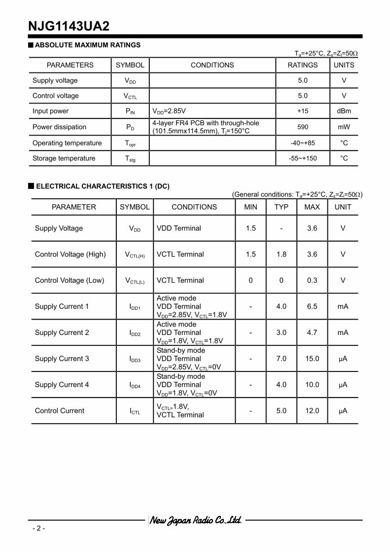
ELECTRICAL CHARACTERRISTICS
Conditions: VDD=2.85V, VCTL=1.8V, Ta=+25oC, Zs=Zl=50Ω, with application circuit
S11, S22 S21, S12
VSWR Zin, Zout
S11, S22 (f=50MHz~20GHz) S21, S12 (f=50MHz~20GHz)

- 6 -
NJG1143UA2
ELECTRICAL CHARACTERRISTICS
Conditions: VDD=2.85V, VCTL=1.8V, Ta=+25oC, Zs=Zl=50Ω, with application circuit
0
0.5
1
1.5
2
2.5
3
15
16
17
18
19
20
21
1.45 1.5 1.55 1.6 1.65 1.7 1.75
No
ise
Fig
ure
(d
B)
Ga
in (
dB
)
frequency (GHz)
NF
NF, Gain vs. frequency(VDD=2.85V, VCTL=1.8V)
Gain
(NF: Exclude PCB, Connector Losses)
-25
-20
-15
-10
-5
0
5
10
-40 -30 -20 -10 0 10
Po
ut
(dB
m)
Pin (dBm)
P-1dB(IN)=-16.0dBm
Pout
Pout vs. Pin(VDD=2.85V, VCTL=1.8V, fRF=1575MHz)
8
10
12
14
16
18
20
22
24
2
3
4
5
6
7
8
9
10
-40 -30 -20 -10 0 10
Ga
in (
dB
)
IDD (
mA
)
Pin (dBm)
Gain
IDD
Gain, IDD vs. Pin(VDD=2.85V, VCTL=1.8V, fRF=1575MHz)
P-1dB(IN)=-16.0dBm
-100
-80
-60
-40
-20
0
20
-40 -30 -20 -10 0 10
Po
ut,
IM
3 (
dB
m)
Pin (dBm)
IIP3=-1.3dBm
Pout
IM3
Pout, IM3 vs. Pin(VDD=2.85V, VCTL=1.8V, fRF=1575+1575.1MHz)
8
10
12
14
16
18
20
22
24
-6
-4
-2
0
2
4
6
8
10
1.45 1.5 1.55 1.6 1.65 1.7 1.75
OIP
3 (
dB
m)
IIP
3 (
dB
m)
frequency (GHz)
OIP3
OIP3, IIP3 vs. frequency(VDD=2.85V, VCTL=1.8V, df=100kHz, Pin=-34dBm)
IIP3
0
1
2
3
4
5
6
0
5
10
15
20
25
30
0 0.5 1 1.5 2 2.5 3
IDD (
mA
)
ICT
L (
uA
)
VCTL (V)
IDD
IDD, ICTL vs. VCTL(VDD=2.85V, RF OFF)
ICTL

NJG1143UA2
- 7 -
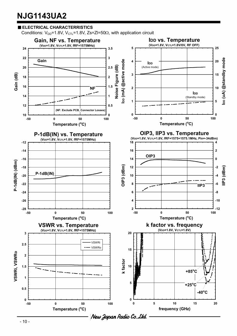
ELECTRICAL CHARACTERRISTICS
Conditions: VDD=2.85V, VCTL=1.8V, Ta=+25oC, Zs=Zl=50Ω, with application circuit
10
12
14
16
18
20
22
24
0
0.5
1
1.5
2
2.5
3
3.5
-50 0 50 100
Gain
(d
B)
No
ise
Fig
ure
(d
B)
Temperature (oC)
NF
Gain, NF vs. Temperature(VDD=2.85V, VCTL=1.8V, fRF=1575MHz)
Gain
(NF: Exclude PCB, Connector Losses)
-24
-22
-20
-18
-16
-14
-12
-10
-8
-50 0 50 100
P-1
dB
(IN
) (d
Bm
)
Temperature (oC)
P-1dB(IN) vs. Temperature(VDD=2.85V, VCTL=1.8V, fRF=1575MHz)
P-1dB(IN)
5
10
15
20
25
30
-10
-5
0
5
10
15
-50 0 50 100
OIP
3 (
dB
m)
IIP
3 (
dB
m)
Temperature (oC)
IIP3
OIP3, IIP3 vs. Temperature(VDD=2.85V, VCTL=1.8V, fRF=1575+1575.1MHz, Pin=-34dBm)
OIP3
0
0.5
1
1.5
2
2.5
3
-50 0 50 100
VSWRi
VSWRo
VS
WR
i, V
SW
Ro
Temperature (oC)
VSWR vs. Temperature(VDD=2.85V, VCTL=1.8V, fRF=1575MHz)
0
5
10
15
20
0 5 10 15 20
k f
ac
tor
frequency (GHz)
k factor vs. frequency(VDD=2.85V, VCTL=1.8V)
+85oC
+25oC
-40oC
0
1
2
3
4
5
6
0
5
10
15
20
25
30
-50 0 50 100ID
D (
mA
) @
acti
ve
mo
de
IDD (
uA
) @
sta
nd
by
mo
de
Temperature (oC)
IDD vs. Temperature(VDD=2.85V, VCTL=1.8V/0V, RF OFF)
IDD
(Active mode)
IDD
(Standby mode)

- 8 -
NJG1143UA2
ELECTRICAL CHARACTERRISTICS
Conditions: VDD=1.8V, VCTL=1.8V, Ta=+25oC, Zs=Zl=50Ω, with application circuit
S11, S22 S21, S12
VSWR Zin, Zout
S11, S22 (f=50MHz~20GHz) S21, S12 (f=50MHz~20GHz)
NJG1143UA2
- 9 -
ELECTRICAL CHARACTERRISTICS
Conditions: VDD=1.8V, VCTL=1.8V, Ta=+25oC, Zs=Zl=50Ω, with application circuit
0
1
2
3
4
5
6
0
5
10
15
20
25
30
0 0.5 1 1.5 2 2.5 3
IDD (
mA
)
ICT
L (
uA
)
VCTL (V)
IDD
IDD, ICTL vs. VCTL(VDD=1.8V, RF OFF)
ICTL
0
0.5
1
1.5
2
2.5
3
15
16
17
18
19
20
21
1.45 1.5 1.55 1.6 1.65 1.7 1.75
No
ise F
igu
re (
dB
)
Ga
in (
dB
)
frequency (GHz)
NF
NF, Gain vs. frequency(VDD=1.8V, VCTL=1.8V)
Gain
(NF: Exclude PCB, Connector Losses)
-100
-80
-60
-40
-20
0
20
-40 -30 -20 -10 0 10
Po
ut,
IM
3 (
dB
m)
Pin (dBm)
IIP3=-5.6dBm
Pout
IM3
Pout, IM3 vs. Pin(VDD=1.8V, VCTL=1.8V, fRF=1575+1575.1MHz)
4
6
8
10
12
14
16
18
20
-10
-8
-6
-4
-2
0
2
4
6
1.45 1.5 1.55 1.6 1.65 1.7 1.75
OIP
3 (
dB
m)
IIP
3 (
dB
m)
frequency (GHz)
OIP3
OIP3, IIP3 vs. frequency(VDD=1.8V, VCTL=1.8V, df=100kHz, Pin=-34dBm)
IIP3
8
10
12
14
16
18
20
22
24
1
2
3
4
5
6
7
8
9
-40 -30 -20 -10 0 10
Gain
(d
B)
IDD (
mA
)
Pin (dBm)
Gain
IDD
Gain, IDD vs. Pin(VDD=1.8V, VCTL=1.8V, fRF=1575MHz)
P-1dB(IN)=-20.0dBm
-30
-25
-20
-15
-10
-5
0
5
-40 -30 -20 -10 0 10
Po
ut
(dB
m)
Pin (dBm)
P-1dB(IN)=-20.0dBm
Pout
Pout vs. Pin(VDD=1.8V, VCTL=1.8V, fRF=1575MHz)
- 10 -
NJG1143UA2
ELECTRICAL CHARACTERRISTICS
Conditions: VDD=1.8V, VCTL=1.8V, Zs=Zl=50Ω, with application circuit
10
12
14
16
18
20
22
24
0
0.5
1
1.5
2
2.5
3
3.5
-50 0 50 100
Gain
(d
B)
No
ise
Fig
ure
(d
B)
Temperature (oC)
NF
Gain, NF vs. Temperature(VDD=1.8V, VCTL=1.8V, fRF=1575MHz)
Gain
(NF: Exclude PCB, Connector Losses)
2
4
6
8
10
12
14
16
18
-12
-10
-8
-6
-4
-2
0
2
4
-50 0 50 100
OIP
3 (
dB
m)
IIP
3 (
dB
m)
Temperature (oC)
IIP3
OIP3, IIP3 vs. Temperature(VDD=1.8V, VCTL=1.8V, fRF=1575+1575.1MHz, Pin=-34dBm)
OIP3
0
5
10
15
20
0 5 10 15 20
k f
ac
tor
frequency (GHz)
k factor vs. frequency(VDD=1.8V, VCTL=1.8V)
+85oC
+25oC
-40oC
-28
-26
-24
-22
-20
-18
-16
-14
-12
-50 0 50 100
P-1
dB
(IN
) (d
Bm
)
Temperature (oC)
P-1dB(IN) vs. Temperature(VDD=1.8V, VCTL=1.8V, fRF=1575MHz)
P-1dB(IN)
0
0.5
1
1.5
2
2.5
3
-50 0 50 100
VSWRi
VSWRo
VS
WR
i, V
SW
Ro
Temperature (oC)
VSWR vs. Temperature(VDD=1.8V, VCTL=1.8V, fRF=1575MHz)
0
1
2
3
4
5
0
5
10
15
20
25
-50 0 50 100
IDD (
mA
) @
acti
ve
mo
de
IDD (
uA
) @
sta
nd
by
mo
de
Temperature (oC)
IDD vs. Temperature(VDD=1.8V, VCTL=1.8V/0V, RF OFF)
IDD
(Active mode)
IDD
(Standby mode)
NJG1143UA2
- 11 -
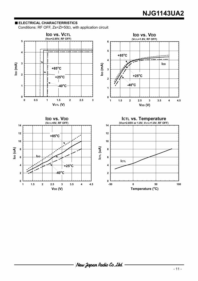
ELECTRICAL CHARACTERRISTICS
Conditions: RF OFF, Zs=Zl=50Ω, with application circuit
0
2
4
6
8
10
12
14
-50 0 50 100
ICT
L (
uA
)
Temperature (oC)
ICTL vs. Temperature(VDD=2.85V or 1.8V, VCTL=1.8V, RF OFF)
ICTL
0
1
2
3
4
5
0 0.5 1 1.5 2 2.5 3
IDD (
mA
)
VCTL (V)
IDD vs. VCTL(VDD=2.85V, RF OFF)
+85oC
+25oC
-40oC
0
1
2
3
4
5
6
1 1.5 2 2.5 3 3.5 4 4.5ID
D (
mA
)VDD (V)
IDD vs. VDD(VCTL=1.8V, RF OFF)
+85oC
+25oC
-40oC
IDD
0
2
4
6
8
10
12
14
1 1.5 2 2.5 3 3.5 4 4.5
IDD (
uA
)
VDD (V)
IDD vs. VDD(VCTL=0V, RF OFF)
+85oC
+25oC
-40oC
IDD
- 12 -
NJG1143UA2
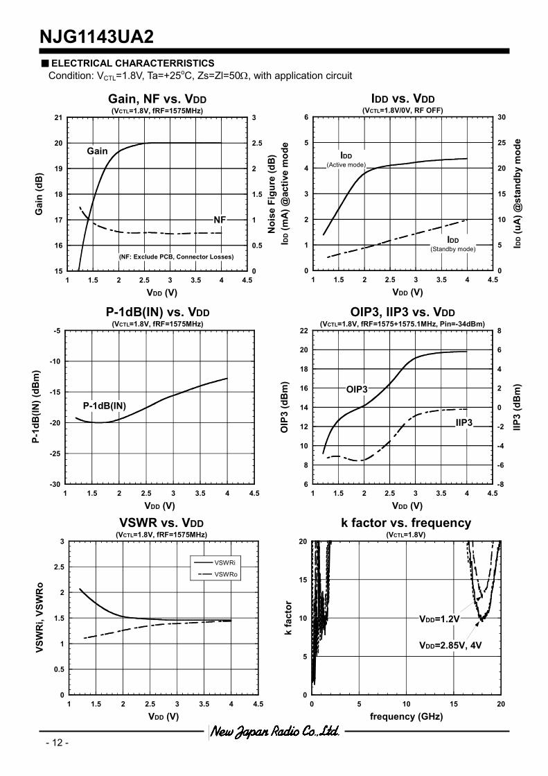
ELECTRICAL CHARACTERRISTICS
Condition: VCTL=1.8V, Ta=+25oC, Zs=Zl=50Ω, with application circuit
15
16
17
18
19
20
21
0
0.5
1
1.5
2
2.5
3
1 1.5 2 2.5 3 3.5 4 4.5
Gain
(d
B)
No
ise
Fig
ure
(d
B)
VDD (V)
NF
Gain, NF vs. VDD(VCTL=1.8V, fRF=1575MHz)
Gain
(NF: Exclude PCB, Connector Losses)
0
1
2
3
4
5
6
0
5
10
15
20
25
30
1 1.5 2 2.5 3 3.5 4 4.5ID
D (
mA
) @
acti
ve
mo
de
IDD (
uA
) @
sta
nd
by
mo
de
VDD (V)
IDD vs. VDD(VCTL=1.8V/0V, RF OFF)
IDD
(Active mode)
IDD
(Standby mode)
6
8
10
12
14
16
18
20
22
-8
-6
-4
-2
0
2
4
6
8
1 1.5 2 2.5 3 3.5 4 4.5
OIP
3 (
dB
m)
IIP
3 (
dB
m)VDD (V)
IIP3
OIP3, IIP3 vs. VDD(VCTL=1.8V, fRF=1575+1575.1MHz, Pin=-34dBm)
OIP3
-30
-25
-20
-15
-10
-5
1 1.5 2 2.5 3 3.5 4 4.5
P-1
dB
(IN
) (d
Bm
)
VDD (V)
P-1dB(IN) vs. VDD(VCTL=1.8V, fRF=1575MHz)
P-1dB(IN)
0
0.5
1
1.5
2
2.5
3
1 1.5 2 2.5 3 3.5 4 4.5
VSWRi
VSWRo
VS
WR
i, V
SW
Ro
VDD (V)
VSWR vs. VDD(VCTL=1.8V, fRF=1575MHz)
0
5
10
15
20
0 5 10 15 20
k f
ac
tor
frequency (GHz)
k factor vs. frequency(VCTL=1.8V)
VDD=1.2V
VDD=2.85V, 4V
NJG1143UA2
- 13 -
1
4
2
3
6
5
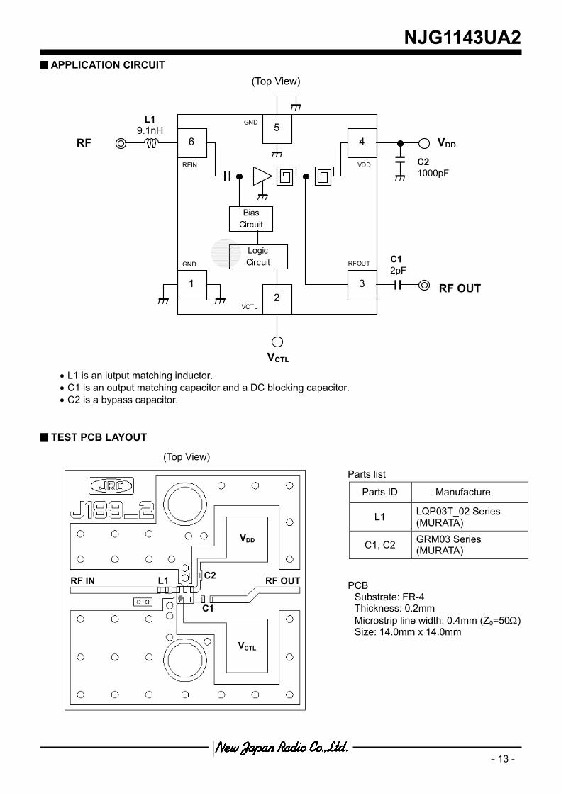
GND
RFIN
RFOUT
VDD
VCTL
GND
Bias
Circuit
Logic
Circuit
L1
9.1nH
VDD RF
RF OUT
C2
1000pF
VCTL
C1
2pF
APPLICATION CIRCUIT
• L1 is an iutput matching inductor.
• C1 is an output matching capacitor and a DC blocking capacitor.
• C2 is a bypass capacitor.
TEST PCB LAYOUT
Parts ID Manufacture
L1 LQP03T_02 Series (MURATA)
C1, C2 GRM03 Series (MURATA)
(Top View)
Parts list
PCB Substrate: FR-4 Thickness: 0.2mm
Microstrip line width: 0.4mm (Z0=50Ω) Size: 14.0mm x 14.0mm
RF IN RF OUT
VDD
VCTL
(Top View)
L1
C1
C2
- 14 -
NJG1143UA2
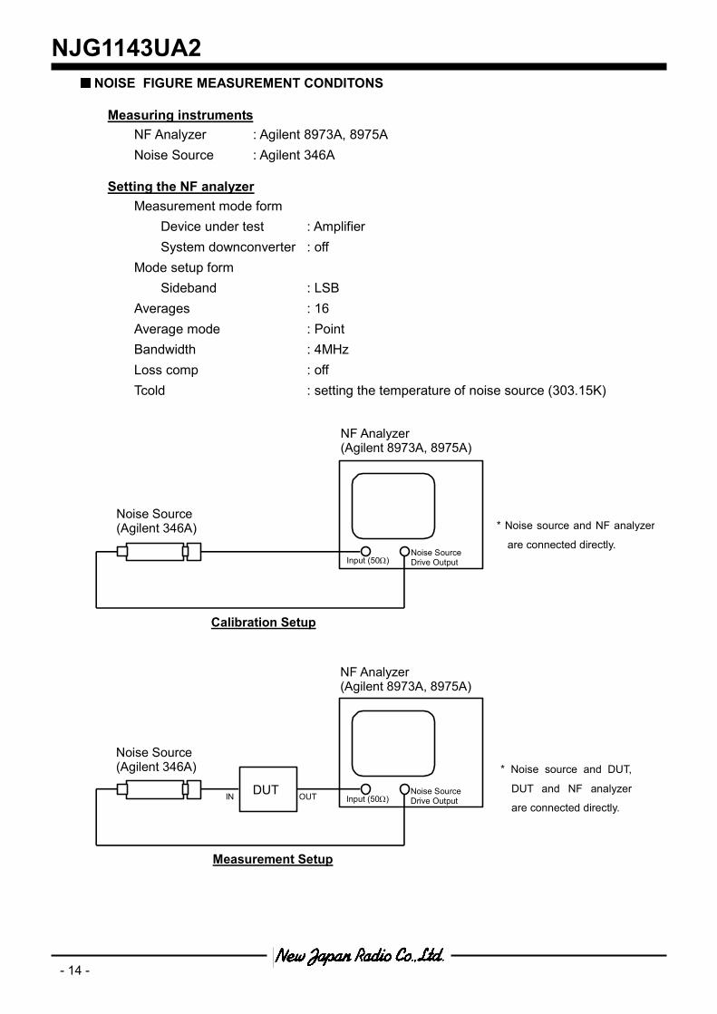
NOISE FIGURE MEASUREMENT CONDITONS
Measuring instruments
NF Analyzer : Agilent 8973A, 8975A
Noise Source : Agilent 346A
Setting the NF analyzer
Measurement mode form
Device under test : Amplifier
System downconverter : off
Mode setup form
Sideband : LSB
Averages : 16
Average mode : Point
Bandwidth : 4MHz
Loss comp : off
Tcold : setting the temperature of noise source (303.15K)
Calibration Setup
Noise Source (Agilent 346A)
NF Analyzer (Agilent 8973A, 8975A)
Input (50Ω) Noise Source Drive Output
* Noise source and NF analyzer
are connected directly.
Measurement Setup
Noise Source (Agilent 346A)
DUT
NF Analyzer (Agilent 8973A, 8975A)
Input (50Ω) Noise Source Drive Output
IN OUT
* Noise source and DUT,
DUT and NF analyzer
are connected directly.

NJG1143UA2
- 15 -
PACKAGE OUTLINE (EPFFP6-A2)
Unit : mm Substrate : FR4 Terminal treat : Au Molding material : Epoxy resin Weight (typ.) : 0.855mg
Cautions on using this product This product contains Gallium-Arsenide (GaAs) which is a harmful material.
• Do NOT eat or put into mouth.
• Do NOT dispose in fire or break up this product.
• Do NOT chemically make gas or powder with this product.
• To waste this product, please obey the relating law of your country.
This product may be damaged with electric static discharge (ESD) or spike voltage. Please handle with care to avoid these damages.
[CAUTION] The specifications on this databook are only given for information , without any guarantee as regards either mistakes or omissions. The application circuits in this databook are described only to show representative usages of the product and not intended for the guarantee or permission of any right including the industrial rights.