Embed Size (px)
Citation preview

THE MICTROSTRUCTURE, MECHANICAL PROPERTIES, AND THERMAL
STABILITY OF TERNARY Cr1-xMoxNy THIN-FILMS
by
YUJIAO ZOU
ANDREI STANISHEVSKY, CHAIR
SHANE AARON CATLEDGE
AMBER L GENAU
GREGG M JANOWSKI
YOGESH K VOHRA
A DISSERTATION
Submitted to the graduate faculty of The University of Alabama at Birmingham,
in partial fulfillment of the requirements for the degree of
Doctor of Philosophy
BIRMINGHAM, ALABAMA
2012

ii
THE MICTROSTRUCTURE, MECHANICAL PROPERTIES, AND THERMAL
STABILITY OF TERNARY Cr1-xMoxNy THIN-FILMS
YUJIAO ZOU
PHYSICS
ABSTRACT
The microstructure, thermal stability and mechanical properties of ternary
chromium molybdenum nitride (Cr-Mo-N) films were studied. In this work, a series of
Cr-Mo-N films with different Cr/Mo ratios were deposited on CoCrMo and silicon
substrates at various deposition temperatures by using a dual rf-magnetron sputtering
system with Cr and Mo targets and nitrogen as reactive gas. Thermal processing at
temperatures up to 700 °C in air and up to 800°C in microwave plasma with H2/N2 gas
mixture were employed to evaluate the thermal stability of films. The films’
microstructure was investigated by scanning electron microscope (SEM) and X-ray
Diffraction (XRD). The surface morphology was studied by atomic force microscopy
(AFM), and the chemical composition was analyzed by X-ray photoelectrons
spectroscopy (XPS) and Energy-Dispersive X-ray Spectrometer (EDS). The mechanical
properties were studied by Nanoindentation and Tribometry. The coatings exhibited
mainly face centered cubic (fcc) structure with some secondary phase precipitates. All as
prepared films showed mean grain size 13 – 21 nm and the lattice parameters varying
between those of CrN and γ-Mo2N depending on the composition. The surface roughness
of the films varied from the pure CrN and pure γ-Mo2N in the nanoscale range. The
hardness and Young’s modulus were found in the range of 9.0 - 22 GPa and 175- 330

iii
GPa, respectively, with larger values observed for Mo-rich layers. The coefficient of dry
friction with Ti counterpart varied from 0.41 to 0.67. Thermal stabilities of Cr-Mo-N
coatings during the annealing up to 700°C in air have been studied. It has been found that
Cr1-xMoxNy films with Cr-rich content are more stable than those with Mo-rich content.
All properties were improved by increasing the deposition temperature.
Key words: Magnetron sputtering, Thermal stability, Mechanical property, Chromium
molybdenum nitride

iv
ACKNOWLEDGEMENTS
Time flies! I can't imagine I am going to finish my PhD work soon. The
accomplishment of my PhD would not be achieved without many people to whom I
would like to express my sincere gratitude.
First of all, I would like to express my gratitude to Dr. Andrei Stanishevsky.
During my doctoral studies he directed me to the thin films and surface engineering field,
and guided me through the research, answered many theoretical questions and helped me
with the experimental work. He always endorsed my curiosity and gave me freedom to
pursue different scientific problems.
Secondly, thank Dr. Yogesh K Vohra, it is his Nanoscale Science and
Applications class introduced me to the science of nanotechnology and generated my
research interest in nanostructured thin film materials.
The third to whom I owe great deal is Dr. Shane Aaron Catledge. He unselfishly
shared his knowledge, helped and trained me in many experiment techniques.
My gratitude goes also to Dr. Corinne Nouveau, Issam Rahil, Luc Imhoff, from
Laboratoire Bourguignon des Matériaux et Procédés, CER Arts et Métiers ParisTech of
Cluny, France for performing magnetron sputtering system and TEM/SEM measurements.
A special gratitude goes to my collogue Michael Walock, I am deeply indebted to for his
help and support with my doctoral work.
I would also like to express my gratitude to Gopi Samudrala and Leigh Booth, for
their help with the experiment.

v
I want to express my gratitude to everyone who helped me with the theoretical
and experimental work, and people in Physics department at UAB, for friendly
atmosphere and for help with practical work.
At the end, I would like to thank my parents and friends. Your friendship and
understanding, which I received during the years, helped me to overcome burdens of
tedious scientific research.

vi
TABLE OF CONTENTS
Page
ABSTRACT……………………………………………………………………………..ii
ACKNOWLEDGMENTS………………………………………………………………iv
LIST OF TABLES……………………………………………………………………viii
LIST OF FIGURES…………………………………………………………………….ix
CHAPTER
1. State-of-the-art in hard coatings ……………………………………...…..…...1
1.1. Introduction to hard coatings.......................................................................1
1.2. Review of binary nitride coatings................................................................4
1.3. Review of ternary nitride coatings...............................................................6
1.4. Deposition Methods ...................................................................................7
1.4.1 Magnetron Sputtering.........................................................................9
1.4.2 Cathodic Arcs....................................................................................13
1.5. Influence of deposition parameters on film's microstructure.....................14
1.6. Stress in the films.......................................................................................16
1.7. Structure/property relationship for hard coatings......................................17
1.8. Case of ternary CrMoN coatings...............................................................18
1.9. Goals of the research..................................................................................19
2. Experimental approaches ................................................................................21
2.1. Equipment and procedures.........................................................................21
2.2. Characterization techniques ......................................................................26
2.2.1 Characterization of film's structure...................................................26
2.2.1.1 Scanning Electron Microscopy (SEM).................................26
2.2.1.2 Transmission Electron Microscopy (TEM)..........................29
2.2.1.3 X-Ray Diffraction (XRD).....................................................31
2.2.1.4 Atomic Force Microscopy (AFM)........................................33
2.2.2 Characterization of film's composition.............................................37
2.2.2.1 X-ray Photoelectron Spectroscopy (XPS)............................37
2.2.2.2 Energy Dispersive X-ray Spectrometry (EDS).....................39

vii
2.2.3 Characterization of film's mechanical properties..............................40
2.2.3.1 Nanoindentation....................................................................40
2.2.3.2 Tribometry............................................................................44
2.2.3.3 Stress measurements.............................................................46
3. Cr-Mo-N coatings on CoCrMo substrates.......................................................48
3.1. Sample preparation....................................................................................48
3.1.1 Film deposition.................................................................................48
3.1.2 Thermal processing of films.............................................................48
3.2. Experimental results of structure and morphology....................................49
3.2.1 Scanning Electron Microscopy (SEM).............................................50
3.2.2 X-Ray Diffraction (XRD).................................................................50
3.2.3 X-ray Photoelectron Spectroscopy (XPS)........................................52
3.2.4 Atomic Force Microscopy (AFM)....................................................56
3.3. Mechanical properties................................................................................58
3.3.1 Nanoindentation................................................................................58
4. Cr1-xMoxNy coatings on Si substrates...........................................................62
4.1. Samples preparation...................................................................................62
4.1.1 Film deposition.................................................................................62
4.1.2 Thermal processing of films.............................................................63
4.2. Experimental results of structure and morphology....................................64
4.2.1 Scanning Electron Microscopy (SEM).............................................64
4.2.2 X-Ray Diffraction (XRD).................................................................67
4.2.3 Transmission Electron Microscopy (TEM)......................................76
4.2.4 X-ray Photoelectron Spectroscopy (XPS)........................................77
4.2.5 Energy Dispersive X-ray Spectrometry (EDS).................................82
4.2.6 Stress.................................................................................................83
4.2.7 Atomic Force Microscopy (AFM)....................................................84
4.3. Mechanical properties................................................................................86
4.3.1 Nanoindentation ...............................................................................86
4.3.2 Tribology...........................................................................................92
5. Discussion and Conclusion..............................................................................97
LIST OF REFERENCES.................................................................................................102

viii
LIST OF TABLES
Table Page
Table1.1 Selected properties of metallic hard materials.........................................6
Table 3.1 Overview of CrMoN coatings with different thermal processes......................49
Table 3.2 Mechanical properties and surface roughness overview of the CrMoN
coatings under various thermal processes..............................................................59
Table 4.1 Deposition parameters of the as-deposited Cr1-xMoxNy coatings on Si
substrates................................................................................................................62
Table 4.2 Chemical composition of the Cr 1 -xMoxNy coatings deposited at
400°C.....................................................................................................................81
Table 4.3 Residual stress in the Cr1-xMoxNy coatings deposited at 400°C............82
Table 4.4 Deposition parameters of multilayer coatings CrN/MoN (m1),(m2) and single
layer Cr25Mo25N50 coatings deposited at room temperature (c1) and high
temperature (c2).....................................................................................................89
Table 4.5 Selected properties overview of the Cr-Mo-N coatings deposited at
400°C.....................................................................................................................94

ix
LIST OF FIGURES
Figure Page
Fig1.1 Growth of production in German machine industry.....................................2
Fig1.2 Standard coatings developed in the last three decades........................... ......3
Fig1.3 Film vapor deposition process flow diagram........................................ .......7
Fig1.4 Schematic diagram of a typical magnetron sputtering system.......... .........11
Fig1.5 Schematic diagram of a typical cathodic arc source................ ...................13
Fig1.6 Structure Zone Diagram for plasma based thin film deposition.... .............16
Fig2.1 The Nordiko 3500 RF magnetron sputtering system......................... .........21
Fig2.2 The vacuum diagram of the magnetron sputtering system............... ..........22
Fig2.3 Guns arrangement of the sputtering system........ .......................................23
Fig2.4 Substrate holder in the chamber of the sputtering system.............. ............24
Fig2.5 The electrode beneath the substrate holder................................. ................25
Fig2.6 Schematic diagram of a typical Scanning Electron Microscopy....... .........27
Fig2.7 Mechanism of the beam hitting sample in a SEM......................... .............28
Fig2.8 Schematic diagram of a typical Transmission Electron Microscopy... ......30
Fig2.9 Diagram of Bragg's Law............................................................. ...............31
Fig2.10 Schematic diagram of the X-ray beam detection in XRD.......................32
Fig 2.11 a)Spring depiction of cantilever b) SEM image of triangular SPM cantilever
with probe (tip)....................................................................... ...............34
x
Fig2.12 Schematic of AFM instrument showing "beam bounce" method of detection
using a laser and position sensitive photodiode detector.............. .........35
Fig2.13 Plot of force as a function of probe-sample separation............................36
Fig2.14 Ideally a probe (tip) with a high aspect ratio will give the best resolution. The
radius of curvature of the probe leads to tip convolution. This does not often
influence the height of a feature but the lateral resolution.....................................37
Fig2.15 The mechanism of X-ray ejecting electrons in XPS.................................38
Fig2.16 A typical load-displacement curve of fused silica....................................41
Fig2.17 Load-displacement curve showing the unloading (Su) and loading (Sl) slopes
used in calculation of hardness and Young's modulus. Also indicated is the plastic
work of indentation Wp which is the area bounded by the loading and unloading
curves and the displacement axis....................... ...................................43
Fig2.18 The mechanism diagram of the tribometer.......... .....................................45
Fig2.19 An image of a typical CSM nanotribometer........................ .....................45
Fig2.20 Image of a Wyko NT1100 Profilometer......................... ..........................47
Fig3.1. A cross-sectional scanning electron micrograph of the as-prepared Cr25Mo25N50
coating............................................................................ ..................50
Fig3.2 X-ray diffraction patterns of (1) as-deposited CrMoN ternary film, (2) annealed in
a i r a t 8 00° C , and (3 ) ann ea led i n H 2 /N 2 m ic ro wave p l a sma a t
800°C.....................................................................................................................51
Fig3.3 XPS results of (1) as deposited CrMoN coating........................................52
Fig3.4 XPS results of (2) CrMoN coating annealed in air at 800°C.....................53
Fig3.5 XPS results of (3) CrMoN coating annealed in mw plasma at 800°C.......54

xi
Fig3.6 XPS results of (4) annealed in air at 600°C+in mw plasma at 800°C ….. 55
Fig3.7 XPS results of (5) annealed in mw plasma at 800°C+in air at 800°C .... ...55
Fig3.8 Atomic Force Microscopy (AFM) results of Cr25Mo25N50 coatings under different
treatments (1) as deposited Cr25Mo25N50 coating (2) annealed in air at 800°C (3)
annealed in mw plasma at 800°C................... .......................................56
Fig3.9 AFM picture of (4) annealed in air at 600°C+in mw plasma (5) annealed in mw
plasma +in air at 800°C..................................................................................57
Fig3.10 Mechanical properties of (1) as deposited CrMoN coating (2) annealed in air at
800°C (3) annealed in mw plasma at 800°C (4) annealed in air at 600°C+in mw
plasma (5) annealed in mw plasma +in air at 800°C......................................59
Fig4.1 SEM cross-section image of (c1) Cr25Mo25N50 and (b1) Cr32Mo18N50 films
deposited at room temperature...............................................................................63
Fig4.2 The surface morphology SEM images of the as-deposited (a1)CrN (b1)
Cr32Mo18N50 (c1) Cr25Mo25N50 (d1) Cr18Mo32N50 (e1)MoN coatings deposited at
room temperature...................................................................................................64
Fig4.3 Cross sectional and surface SEM pictures of (a2)CrN (b2)Cr 32Mo18N50
(c2)Cr25Mo25N50 (d2)Cr18Mo32N50 (e2)MoN coatings deposited at 400°C...........64
Fig4.4 SEM picture of as deposited (a2)CrN (b2)Cr32Mo18N50 (c2)Cr25Mo25N50
(d2)Cr18Mo32N50 (e2)MoN coatings deposited at 400°C annealed in air at
600°C.....................................................................................................................65
Fig4.5 SEM picture of (a2)CrN (b2)Cr32Mo18N50 (c2)Cr25Mo25N50 coatings deposited at
400°C annealed in air at 700°C.............................................. ...........66

xii
Fig4.6 XRD patterns of as deposited (a1)CrN (b1)Cr32Mo18N50 (c1)Cr25Mo25N50
(d1)Cr18Mo32N50 (e1)MoN deposited at room temperature...................................67
Fig4.7 XRD patterns of (a1)CrN (b1)Cr32Mo18N50 (c1)Cr25Mo25N50 (d1)Cr18Mo32N50
(e1)MoN deposi ted at room temperature af ter annealed at ai r at
600°C.....................................................................................................................68
Fig4.8 XRD patterns of (a1)CrN (b1)Cr32Mo18N50 (c1)Cr25Mo25N50 deposited at room
temperature after annealed at air at 700°C............................... ....................68
Fig4.9 XRD patterns of (a2)CrN as deposited at 400°C and under thermal
processes................................................................................................................69
Fig4.10 XRD patterns of (e)MoN as deposited at 400°C and under thermal
processes................................................................................................................71
Fig4.11 XRD patterns of (d2) Cr18Mo32N50 as deposited at 400°C and under thermal
processes.............................................. .....................................................72
Fig4.12 XRD patterns of (b2) Cr32Mo18N50 as deposited at 400°C and under thermal
processes.................................................... ...............................................73
Fig4.13 XRD patterns of (c2) Cr25Mo25N50 as deposited at 400°C and under thermal
processes........................................... ........................................................74
Fig4.14 Lattice parameters CrxN and MoxN selected (111) or (200) crystal plane as a
function of Mo content......................................................... ..........................75
Fig4.15 TEM high magnification cross-sectional and surface morphology of (c1)
Cr25Mo25N50 coatings deposited at room temperature...........................................76
Fig4.16 XPS results of (a1)CrN (c1) Cr25Mo25N50 (e1)MoN coatings deposited at room
temperature................................................................................ ...................78

xiii
Fig4.17 XPS results of as deposited (a2)CrN (b2)Cr32Mo18N50 (c2)Cr25Mo25N50
(d2)Cr18Mo32N50 (e2)MoN coatings deposited at 400°C...................................80
Fig4.18 AFM images of (a1)CrN (b1)Cr32Mo18N50 (c1)Cr25Mo25N50 (d1)Cr18Mo32N50
(e1)MoN coat ings deposited at room temperature. . . . . . . . . . . . . . . . . . . .83
Fig4.19 Surface roughness changes of (a1)CrN (b1)Cr32Mo18N50 (c1)Cr25Mo25N50
deposited at room temperature after annealing processes……………………......84
Fig4.20 Surface roughness changes of (a2)CrN (b2)Cr32Mo18N50 (c2)Cr25Mo25N50
(d2)Cr18Mo32N50 (e2)MoN coatings deposited at 400°C after annealing
processes................................................................................................................85
Fig4.21 Hardness and Young’s Modulus changes of (a1)CrN (b1)Cr32Mo18N50
(c1)Cr25Mo25N50 (d1)Cr18Mo32N50 (e1)MoN coatings deposited at room
temperature after annealing processes...................................................................86
Fig4.22 Hardness and Young’s Modulus of (a2)CrN (b2)Cr32Mo18N50 (c2)Cr25Mo25N50
(d2)Cr 1 8 Mo3 2 N5 0 (e2)MoN coat ings deposi ted at 400°C. . . . . . . . . . .87
Fig4.23 Hardness and Young’s Modulus changes of (a)CrN (b)Cr 32Mo18N50
(c)Cr25Mo25N50 coatings deposited at 400°C after thermal processes...................88
Fig4.24 Cross-sectional SEM images of multilayer CrN/MoN (m1) and (m2)
coatings..................................................................................................................89
Fig4.25 Surface morphology SEM and AFM images showing the surface roughness of
multilayer CrN/MoN coatings.............................................. ............90
Fig4.26 Mechanical properties of multilayer CrN/MoN coatings compared with the
Cr25Mo25N50 coatings.......................................................................................91

xiv
Fig4.27 Coefficient of Friction (COF) of Cr1-xMoxNy coatings deposited at
200 °C....................................................................................................................92
Fig4.28 Coefficient of Friction (COF) of Cr1-xMoxNy coatings deposited at
400 °C....................................................................................................................93
Fig5.1 Chromium-Molybdenum-Nitrogen ternary alloy phase diagram (based on 1991
Frisk K.)........................................................................................................96

1
CHAPTER 1
STATE-OF-THE-ART IN HARD COATINGS
1.1 Introduction to hard coatings
Hard coatings are thin layered coatings, which are deposited on the bulk
substrates in order to achieve the desired properties of the surface, such as high hardness,
low friction, high wear resistance and corrosion resistance while leaving the properties of
the bulk materials unchanged. The term “hard coatings,” technically speaking, covers a
broad spectrum of materials. Hard materials for coatings can be divided in three groups
depending on the chemical bonding character. It includes metallic hard materials (borides,
carbides, and nitrides of the transition metals), covalent hard materials (borides, carbides
and nitrides of Al, Si, and B, as well as diamond), and ionic (ceramic) hard materials
(oxides of Al, Zr, Ti, and Be). [1]
Some applications such as industrial machine parts, drillings, and bearings require
the tribological coatings with low coefficient of friction. The term, “tribology”, comes
from the Greek word, tríbein, meaning to rub, is the study of the friction and wear of
materials [2]
. The tribology plays an important role in tool service life. In manufacturing,
friction increases tool wear and the power required to work a piece, which results in
increased costs due to more cutting fluid consumed, the loss of tolerance as tool
dimensions shift, and greater forces required to shape a piece. In biomedical implant
applications, the wear of devices increases the frequency of replacement, then brought
more suffer and pain for patients.

2
The high hardness in combination with a low coefficient of friction decreases the
rate of abrasive wear of the coated component.
Fig.1.1 Growth of production in German machine industry
Fig.1.1 is provided by the VDMA (Verband Deutscher Maschinen- und
Anlagenbau - German Engineering Federation); one of the key association service
providers in Europe, and it shows the growth of production in German machine industry.
Compared to the statistical of base year 2000, the growth of production is 21% for
machine manufacturers and 17% for tool manufacturers, respectively. The surface
treatment industry has shown an increase of 110% with the majority realised by thin film
coating technologies, 72% in Europe and 54% in the USA [3,4]
.
Coating provides tools high performance to save costs on modern manufacturing.
Testing has demonstrated as much as a 100~300% increase in tool life and up to a
20~40% increase in cutting speed in comparison with uncoated tools. The coatings can

3
increase speeds of machining, reduce cycle times and increase productivity, prolong the
tool durability and life; reduce down time and tool-changing cost [5]
.
The first tribological coating for controlling friction and wear was titanium
carbide (TiC), introduced in 1969 on cemented carbide cutting tool inserts using chemical
vapor deposition (CVD)[6]
. The problem with the CVD process was that the substrate
temperature during deposition was about 1000ºC so that CVD could not be used to coat
high speed steel tooling, which is softened at those temperatures. To overcome this
obstacle, industry began using physical vapor deposition (PVD) techniques that provide
ion bombardment of the growing film, resulting in good film adhesion and densification.
Since the first PVD coating material, TiN, was introduced for cutting tools in the
early 1980s, PVD coating on cutting tools have saved companies billions in expenses[3]
.
Fig.1.2 Standard coatings developed in the last three decades

4
Fig 1.2 is provided by LMT(Leading Metalworking Technologies) in Germany.
The Fig 1.2 shows the development of coating technology on the cutting tool industry.
Coating technology for cutting tools has developed rapidly. In 1980, only the TiN coating
and until 1988 only TiCN and CrN were used. In 2000, 14 standard coatings became
available. Considering the different stoichiometries and structures, it can be seen that
several hundred different coatings are now available. In the case of coatings with
different chemical compositions, there are 70 or so different coatings on the market.
1.2 Review of binary nitride coatings
Intensive development of the superhard coatings such as single element diamond
(diamond-like-carbon DLC) and cubic boron nitride (CBN) peaked in the 90’s. It seems
that an insurmountable technical barrier – extremely high residual stress during
deposition – has not been overcome and still prevents successful commercialization [3]
.
The first commercially successful PVD hard coating was titanium nitride (TiN).
TiN coatings provide wear resistance, reduce friction, maintain sharp edges, and improve
surface hardness. Some companies have achieved the TiN coatings successfully. For
example, Balzers deposited it with their low voltage electron beam process, Ulvac with
their hot hollow cathode process, and Multi-Arc with their cathodic arc process. Since the
cost of the arc coating equipment was less than that of competing deposition processes,
the cost of the arc coatings was lower, and the use of cathodic arc deposited hard coatings
became widespread.
Initially, sputtering was not used for the commercial deposition of the tribological
films because the quality of the films did not equal that of films produced by low voltage

5
electron beam or cathodic arc methods. This situation was significantly improved with
the introduction of closed-field unbalanced magnetron sputtering that provided for a
higher degree of substrate ion bombardment during deposition.
One of the early themes in PVD tribological coatings was their high hardness. It is
true that a coating used for a machining application must be hard, but it is now
understood that a coating should be both hard and ductile if it is going to perform well in
a tribological application, and it has been shown by Leyland and Matthews[7,8]
.
The commercial acceptance of hard coatings for cutting tools is driven by
demands on machining productivity, environmental mandates, and increased usage of
new difficult-to-cut materials (e.g.Ti-6Al-4V and Inconel 718). Improved cutting
performance is derived from synergies of machine tool system and cutting tool
development. The latter strives for an optimized combination of tool material, hard
coating and cutting edge geometry.
In industry, the tools are always exposed to increased temperature, high oxidation
and other severe environments, so besides the high hardness and ductility, the coatings
need high thermal stability, oxidation resistance, and corrosion resistance. The hard
nitride coatings are suitable, and now commonly used in a wide range of tribological
applications to improve performance and to extend the life of metal cutting, drilling, and
forming tools, as well as bearings and various machine parts.
Table 1.1 show selected properties of important representative of the metallic hard
materials. All the compounds stand out for their high hardness and high melting points.

6
Table 1.1 Selected properties of metallic hard materials [9]
The most commonly used nitride coatings which include TiN, CrN, MoN , ZrN,
WN, AlN, BN. etc, have been well studied [10,11,12,13,14,15]
. For example, CrN has excellent
corrosion resistance, oxidation resistance, and good wear resistance, for the oxidation
behaviour, linear increase in the surface roughness and surface grain size with the oxide
layer thickness was found[ 16 ]
, however, the better mechanical properties are still
desirable. Cr2O3 is the hardest material among all oxides. It has a high hardness of 29
GPa as compared to 12 GPa for silicon dioxide and 22 GPa for alumina. [17]
1.3 Review of ternary nitride coatings
Ternary nitride films can, under appropriate conditions, form coating systems
with a combination of useful properties similar to or better than those of binary nitrides. It
has been reported that TiAlN and TiZrN films have superior wear resistance compared to
binary TiN films [ 18 , 19 , 20 ]
. Reactive cathodic sputtered TiCrN exhibited improved

7
corrosion behavior when compared with TiN 21
. Ternary Cr-X-N(X=Ti, Al, Si, C, B, Ta,
Nb, Ni) [22,23,24,25,26,27,28,29,30,31,32,33]
coatings have been explored as an evolutionary step
from CrN coatings. The TiAlN PVD coating is currently the most widely deposited PVD
coating for cutting tools, however, for certain particular applications, TiCN and CrN offer
better solutions when the coefficient of friction is critical. Nanocrystalline CrCN coating
has been found with higher hardness than CrN and good coefficient friction values
depending on C content added.[34]
1.4 Deposition Methods
Vapor deposition processes can principally be divided into two types, (1) physical
vapor deposition (PVD) and chemical vapor deposition (CVD). PVD processes involve
the creation of materials vapors by evaporation, sputtering, or laser ablation, and their
subsequent condensation onto a substrate to form the film. CVD processes are generally
defined as the deposition of a solid material from the vapor phase onto a heated substrate
as a result of chemical reactions [35,36]
. No matter PVD or CVD techniques were used, the
film deposition can be modeled in terms of three steps [37]
.
Fig. 1.3 Film vapor deposition process flow diagram

8
Fig 1.3 shows the three steps of the film deposition process.
Step1: Creation of Vapor Phase Species source can be converted into the vapor
phase by evaporation, sputtering, laser ablation, vapors, or delivered as precursor gases,
etc.
Step2: Transport from source to substrate-The vapor species are transported from
the source to the substrate. During transport, some of the vapor species can be ionized by
creating plasma in this space.
Step3: Film growth on the substrate-This process involves the condensation of the
vapor species onto the substrate and subsequent formation of the film by nucleation and
growth processes. The nucleation and growth processes can be strongly influenced by
bombardment of the growing film by ionic species resulting in a change in microstructure,
composition impurities, and residual stress.
The degree of independent control of these three steps determines the versatility
or flexibility of the deposition process. For example, these three steps can be
independently controlled in PVD process, and, therefore, give greater degree of flexibility
in controlling the structure, properties, and deposition rate, whereas all of the three steps
take place simultaneously at the substrate, and cannot be independently controlled in the
CVD processes.
Physical Vapor Deposition (PVD) coating technology for cutting tools has
multiple successful commercial applications over the last 30 years. Most cutting tools are
PVD coated. The basic PVD processes fall into two general categories: (1) sputtering and
(2) evaporation.

9
Sputtering is the phenomena of momentum transfer from an incident energetic
projectile to a solid or liquid target resulting in the ejection of surface atoms or molecules.
In the sputter deposition process, the target, (a source of coating material) and the
substrate are placed in the vacuum chamber, and evacuated to a pressure typically in the
rage of 10-4
to 10-7
torr. The target (also called a cathode) is connected to a negative
voltage supply, and the substrate generally faces the target. An electric discharge is
initiated after an inert gas (usually argon gas) is introduced into evacuated chamber.
Typical working pressure is in the range of 20-150 mtorr.
In evaporation process, vapors are produced from a source material which is
heated by various methods. It consists of an evaporation source to vaporize the desired
material, and the substrates which are located at an appropriate distance facing the
evaporation source. Resistance, induction, arc electron beam, or lasers are the possible
heat sources for evaporation.
Here we only discuss the two most common PVD deposition methods, the
magnetron sputtering and cathodic arcs.
1.4.1 Magnetron sputtering
Magnetron sputtering is an extremely flexible coating technique that can be used
to coat virtually any solid substrate. Sputtering is basically the removal of atomized
material from a solid by energetic bombardment of its surface layers by ions or neutral
particles.
Prior to the sputtering coating process a vacuum of less than one ten millionth of
an atmosphere must be achieved. Once the appropriate pressure has been reached a

10
controlled flow of an inert gas such as argon is introduced. This raises the pressure to the
minimum needed to operate the magnetrons, although it is still only a few ten thousandth
of atmospheric pressure.
When power is supplied to a magnetron, a negative voltage of typically -300V or
more is applied to the target. This negative voltage attracts positive ions to the target
surface. Generally when a positive ion collides with atoms at the surface of a solid an
energy transfer occurs. If the energy transferred to a lattice site is greater than the binding
energy, primary recoil atoms can be created which can collide with other atoms and
distribute their energy via collision cascades. A surface atom becomes sputtered if the
energy transferred to it normal to the surface is larger than about 3 times the surface
binding energy (approximately equal to the heat of sublimation).
Sputtering of a target atom is just one of the possible results of ion bombardment of a
surface. Aside from sputtering the second important process is the emission of secondary
electrons from the target surface. These secondary electrons enable the electronic
discharge to be sustained.
The sputter process has almost no restrictions in the target materials, ranging from
pure metals where a d.c. power supply can be used, to semiconductors and isolators
which require a r.f. power supply or pulsed dc. Deposition can be carried out in either
non reactive (inert gas only) or reactive (inert & reactive gas) discharges with single or
multi-elemental targets.
During the sputter process a magnetic field can be used to trap secondary
electrons close to the target. The electrons follow helical paths around the magnetic field
lines undergoing more ionizing collisions with neutral gases near the target than would

11
otherwise occur. This enhances the ionization of the plasma near the target leading to a
higher sputter rate. It also means that the plasma can be sustained at a lower pressure. The
sputtered atoms are neutrally charged and so are unaffected by the magnetic trap.
Fig 1.4 gives a schematic diagram of a typical magnetron sputtering system.
During sputtering, energized plasma ions strike a ‘target’, which is composed of the
desired coating material. Atoms from that target are dislodged by the impact of the ion
and ejected from the surface with enough energy to travel to and bond with the substrate.
Magnetron sputtering cathodes use powerful magnets to confine the plasma to the region
closest to the ‘target’. This condenses the ion-space ratio, increases the collision rate, and
thus improves deposition rate.
Fig.1.4 Schematic diagram of a typical magnetron sputtering system

12
Magnetron sputtering is commonly used in industry because of its relatively less
cost and the primary advantages of magnetron sputtering are
1) High deposition rates,
2) Ease of sputtering any metal, alloy or compound,
3) High-purity films,
4) Extremely high adhesion of films,
5) Excellent coverage of steps and small features,
6) Ability to coat heat-sensitive substrates,
7) Ease of automation,
8) Excellent uniformity on large-area substrates.
In the simplest of applications the magnetron is used to deposit metallic materials
by DC sputtering. The DC magnetron is the cheapest of magnetron processes. RF
sputtering equipment is more expensive to purchase than a DC magnetron. DC
magnetrons will not work if an insulating target is used, because no current can flow
through it. The solution to this problem is to use an alternating current at high frequency.
RF sputtering was developed to enable the sputtering of dielectric materials and has the
double advantage that it will sputter metals as well.
The utilization of this technique is impeded by the limitations in choice of target
materials, and the difficulties in fabrication of the target. For example, if ferromagnetic
materials are used as the sputtering target, their thickness should be thin enough so as to
be saturated by the magnetic field. Since high power is localized in a selected area in
magnetron sputtering process, targets should be prepared without voids or bubbles to
avoid local melting and spitting[38]
.

13
1.4.2 Cathodic Arcs
Fig. 1.5 shows the schematic diagram of a typical cathodic arc source [39]
. The arc
evaporation process begins with the striking of a high current, low voltage arc on the
surface of a cathode (known as the target) that gives rise to a small (usually a few
micrometers wide), highly energetic emitting area known as a cathode spot. The localized
temperature at the cathode spot is extremely high (around 15000 °C), which results in a
high velocity (10 km/s) jet of vaporized cathode material, leaving a crater behind on the
cathode surface. The cathode spot is only active for a short period of time, then it self-
extinguishes and re-ignites in a new area close to the previous crater.
Cathodic arc plasma deposition has become the technology of choice for hard,
wear and corrosion resistant coatings for a variety of applications. Cathodic arc plasmas
stand out due to their high degree of ionization, with important consequences for film
nucleation, growth, and efficient utilization of substrate bias. Industrial processes often
use cathodic arc plasma in reactive mode.
Fig.1.5 Schematic diagram of a typical cathodic arc source

14
The most frequent application of cathodic arc plasma deposition is the reactive
deposition of compound films such as CrN, ZrN, TiN, TiAlN, and multilayers thereof.
When the compound layer is formed, the metal reacts preferentially with those gases
whose energy of compound formation is large, i.e. with the thermodynamically preferred
gas species. The plasma may contain contamination such as water vapor, which is typical
for high vacuum systems. This issue is especially important for pulsed plasma systems
where the water layer on the arc cathode and chamber wall is periodically “scrubbed” by
the plasma pulse, and where water vapor is partially ionized. Hydrogen can be
incorporated in a film that is supposed to be an oxide or nitride [40]
. The incorporation of
hydrogen can greatly affect the desired coatings properties such as hardness and elastic
modulus [41]
.
Reactive deposition is commercially done at elevated temperature. One reason is
that the deposition process itself heats the substrate. Heating is often utilized to obtain the
desired coating texture. A side effect of elevated temperature is the reduction of hydrogen
incorporation.
Macroparticles are liquid or solid debris particles that are produced at cathode
spots. Macroparticles are a major issue in cathodic arc coatings. For instance, the
corrosion resistance is compromised when a macroparticle is incorporated in the coating,
disrupting the dense, continuous film. Macroparticle filters is a possible direction, but
reduces deposition rate and increases equipment complexity and cost.
1.5 Influence of deposition parameters on film's microstructure

15
Film growth conditions and resulting structure are often summarized
schematically in so-called structure zones, which predict the morphology and
microstructure of a film independently of its materials, as a function of the adatom
mobility. Movchan and Demchishin[42]
were the first to observe that the morphological
structure of evaporated coatings of Ti, Ni, W, ZrO2 and Al2O3 could be related to a
normalized, or reduced temperature T* (Ts/Tm, where Ts is the actual film temperature
during deposition, and Tm is its melting temperature, both in K) .These diagrams have
been developed for thermal evaporation and sputtering[43,44]
, but recently also adapted for
plasma based deposition[45]
. The temperature, T*, is generalized by including a shift
caused by potential energy of arriving particles; the normalized energy, E*, includes
pressure and kinetic energy of bombarding particles and the t* is the net thickness of the
coating.
Fig 1.6 shows the structure zone diagram for plasma based thin film deposition.
The diagram is schematically divided in four zones for different conditions.
In Zone 1 (T*<0.3) a fine-grained structure consisting of textured and fibrous
grains with domed tops and a high density of lattice imperfections and porous grain
boundaries is formed. The structure is produced by a process of continued nucleation of
grains during deposition due to the low adatom mobility (incident atoms stick at the point
of impact) in combination with shadowing effects[46,47]
.
Zone 2 structure (0.3<T*<0.5) is characterized by unconstrained surface diffusion
leading to uniform columnar grains.
Zone 3 (T*>0.5), at high temperature and energy, allows also bulk diffusion with
resulting recrystallization and densification of large grains. Thornton [48
,49]
extended this

16
zone classification to include the bombardment-induced mobility process in sputtering
through the use of sputtering gas pressure parameter. The normalized energy, E*,
includes pressure and kinetic energy of bombarding particles.
Zone T is a transition zone with improved surface diffusion, however limited over
grain boundaries, which results in competitive growth of V-shaped grains. Zone T films
are denser and have a much smoother surface morphology than the two surrounding
zones.
Fig.1.6 Structure Zone Diagram for plasma based thin film deposition [45]
1.6 Stress in the films

17
Films grown by PVD techniques quite often are very highly stressed. The stresses
can be either tensile or compressive, but tensile stresses are in general most damaging.[50]
The thermal stresses in the coating after cooling from the deposition temperature are
tensile when the thermal expansion coefficient of the coating materials is larger than the
one of the substrate and compressive if the reverse is true.
A plate system composed of a stress bearing thin film, of uniform thickness hf,
deposited on a relatively thick substrate, of uniform thickness hs, a simple relation
between the curvature, κ, of the system and the stress,σ( f)
, of the film as follows:
Stoney[51]
formula: σ( f)
=Eshs2 κ /6hf(1−vs)
f and s denote the thin film and substrate, respectively, and E and v are the Young’s
modulus and Poisson’s ratio, respectively.
1.7 Structure/property relationship for hard coatings
The macroscopic properties of a material are strongly dependent on its structure.
Studies of structure/properties relationships are among the most important issues in
material science. Most commonly the structure studies involve the phase, grain and defect
structure. For thin films, the structure/property relationship is particularly important to
study since thin films usually are deposited far from equilibrium conditions. In most
cases, thin films contain a much higher content of lattice defects such as vacancies,
dislocations, and grain boundaries than conventionally prepared bulk materials.
Furthermore, since the material flux during growth of a thin film often is directional, the
microstructure, and thus also most of the physical properties of thin films are often highly
anisotropic. However, due to the complex nature of the deposition process, and the large

18
number of parameters imposing kinetic limitations to the growth process, it is difficult to
predict the microstructure and physical properties of the deposited film from knowledge
of the used deposition conditions.
The most generic feature observed in thin film microstructures is the small grain
size d. The small grain size cause a hardening of the material in agreement with the Hall-
Petch relation [52]
H=H0+kd-1/2
where H is the film hardness, H0 the intrinsic hardness, and k a material
dependent constant. For hardness, the Hall-Petch relation has been found to be valid for d
values as low as 20nm for single-phase metal films. [53,54,55]
As the decrease in crystal size,
the hardness of materials increases, especially for crystal size down to tens of nanometer.
However, a new deformation mechanism called grain boundary sliding replaces the
dislocation activity that dominates deformation process in conventional materials [56]
.
1.8 Case of ternary CrMoN coatings
As mentioned above, the nitrides of group VIB elements stand out from the hard
nitride coatings. CrN has excellent corrosion resistance under severe environment
conditions, superior oxidation resistance, and good wear resistance, however, it has low
toughness [57,58,59]
. MoN has been found to exhibit many attractive physical properties
such as high hardness, low solubility in non-ferrous alloys and low friction, etc [60]
. MoxN
coatings showed good tribological performance due to the formation of MoO3 as a solid
lubricant [61,62,63,64,65,66,67,68]
.
Several reports have indicated that ternary Cr-Mo-N coatings could have
properties superior to MoxN and CrN tailored through the appropriate combinations of Cr

19
and Mo ratio [69,70,71]
. However, the CrMoN coating is not well explored and only limited
findings have been reported.
1.9 Goals of the research
The CoCrMo alloy system is still a material of choice for many articulating
biomedical implants, and the improvement of their performance is important. The
methods to increase the hardness and corrosion resistance of metallic implants include
nitrogen ion implantation, thermal diffusion, and deposition of hard coatings. Many of
these innovations have not been proven to be successful in clinical applications. For
example, nitrogen ion implantation increases the surface hardness and wettability.
However, the ion-implanted surface layer is less than a micrometer in thickness, which
may quickly get worn through. Thermal diffusion hardening of the metallic surface can
produce a thicker surface layer than ion implantation, but scratching and oxidative wear
are still possible. Among the surface modification methods used, a significant
improvement of CoCrMo implant performance has been obtained with TiN, CrN, CrCN
coatings in various combinations, and with nanocrystalline structure[72,73]
. Such a ternary
system is compositionally close to the substrate and may have the potential for improving
the performance of CoCr alloy-based articulating implants when compared to binary CrN
or MoN coating systems.
In the areas of machining and tooling, PVD coatings are widely used to increase
the life and productivity of cutting tools, saving companies billions of dollars worldwide.
PVD coated cutting tools can be run faster, reducing cycle times and enabling the
production of more components in less time. In metal cutting, wear processes exist on the

20
work-piece material. Cutting fluids are commonly used to reduce the wear, which cost
companies today up to 15% of their total production costs. PVD coatings can reduce the
wear resistance, and increase the life of cutting tools reducing tool-changing and cutting
fluids costs. High speed cutting and dry machining involve extremely high temperatures
at the cutting edge. PVD coatings such as TiAlN have incredible thermal stability, hot
hardness and oxidation resistance. PVD coatings can therefore be run dry or with very
limited amount of cutting fluid.
CrMoN coatings are the potential coatings used in a wide range of applications
such as high speed cutting tools, drilling, bearing, and biomedical implants ,etc, their
properties are important to be studied.
The purposes of this research is to (1) prepare CrMoN coatings by magnetron
sputtering system and investigate the microstructure, phase and chemical composition in
dependence on the deposition conditions; (2) investigate the mechanical properties of the
CrMoN coatings; (3) estimate the microstructure/property relationship of the coatings; (4)
study the thermal stability of the Cr1-xMoxNy coatings depending on their composition.

21
CHAPTER 2
EXPERIMENTAL APPROACHES
2.1 Equipment and procedures
Fig 2.1 shows the commercial Nordiko 3500 RF Magnetron Sputtering System. It
equipped with generator modules, a vacuum chamber, and pumps, etc.
Fig 2.1 The Nordiko 3500 RF magnetron sputtering system
Fig. 2.2 is the vacuum diagram for the Nordiko 3500 RF magnetron sputtering
system. Rough vacuum is provided with an Alcatel 2063C rotary vane pump. This pump
has a peak pumping speed of 18 L/s and an ultimate base pressure of 0.02 Pa. From
atmosphere down to about 0.1 Pa, the pressure is monitored by a thermocouple gauge,

22
marked TC-1 (DV-23 gauge tube) on Fig 2.2. Once cross-over is reached (set at ~ 7 Pa),
the high vacuum valve (marked HV in Fig. 2.2) is opened and the cryogenic pump, a CTI
CryoTorr-8 with a Model 8200 air-cooled compressor, takes over the main pumping of
the chamber. The Cryo-Torr 8 has a peak pumping speed of 1500 L/s for air. A cold
cathode Penning gauge (Alcatel CF2P; marked PG on Fig. 2.2), with an Alcatel FN121
controller, is used to measure pressure below 1 Pa. The ultimate pressure of the system is
approximately 5 x 10⁻⁴
Pa.
Fig 2.2 The vacuum diagram of the magnetron sputtering system
In magnetron sputtering, there are primarily two methods: direct current (DC) and
radio frequency (RF). In DC sputtering, the targets are energized with a DC voltage. This
simple approach is great for conducting targets. However, insulating targets suffer from
charge buildup. Eventually, this will kill the plasma, and the deposition. To counter this,
there is RF sputtering.

23
RF applies a modulating potential to the target. This elimates the problem of
charge buildup, and can produce steady plasmas. In addition to insulating targets, RF can
be used for conducting targets, with only a slight degradation in the deposition rate.
Originally, the Nordiko 3500 system was outfitted with only one 100 mm
magnetron sputtering source, with the associated electronics for RF sputtering (Nordiko
SG-1250, 1.25 kW RF generator operating at 13.56 MHz). However, the vacuum
chamber has been modified, and a second 100 mm magnetron sputtering source has been
added, with the associated electronics for RF sputtering at 13.56 MHz. Fig 2.3 shows the
guns arrangement of the sputtering system. The two guns come into the vacuum chamber
from the side, and are in a confocal arrangement for deposition onto the substrate.
Fig 2.3 Guns arrangement of the sputtering system
24
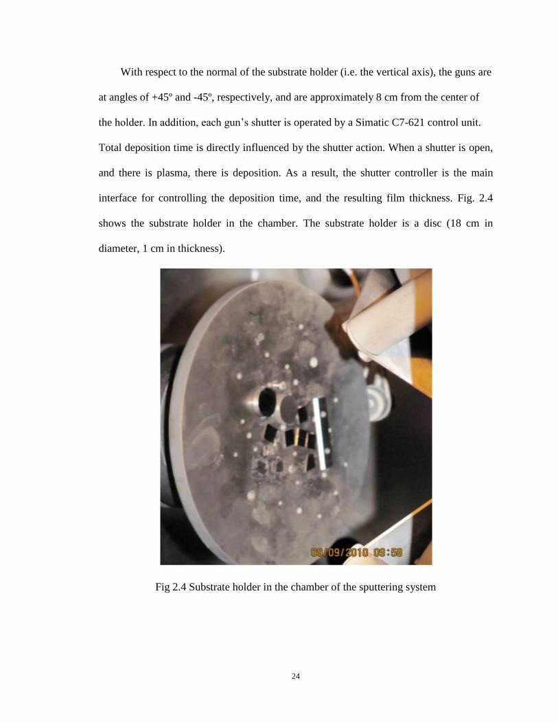
With respect to the normal of the substrate holder (i.e. the vertical axis), the guns are
at angles of +45º and -45º, respectively, and are approximately 8 cm from the center of
the holder. In addition, each gun’s shutter is operated by a Simatic C7-621 control unit.
Total deposition time is directly influenced by the shutter action. When a shutter is open,
and there is plasma, there is deposition. As a result, the shutter controller is the main
interface for controlling the deposition time, and the resulting film thickness. Fig. 2.4
shows the substrate holder in the chamber. The substrate holder is a disc (18 cm in
diameter, 1 cm in thickness).
Fig 2.4 Substrate holder in the chamber of the sputtering system

25
It is mounted vertically, and the samples are typically attached via conductive
carbon tape. The holder is mounted on an alcohol-cooled electrode, which is shown in
Fig. 2.5. This electrode provides the necessary conductive path for both sample cleaning
(prior to deposition) and sample biasing (during deposition).
Fig. 2.5 The electrode beneath the substrate holder
The electrode is accomplished with a pulsed DC power supply (12 kV Physique
& Industrie supply, with digital control). During the sputtering process, the pumping
speed on the chamber is significantly reduced by “closing” the valve marked
ISOLATION on Fig. 2.2. This “valve” does not seal, and the pumps act on this “leak” to
maintain the chamber at the desired pressure during sputtering (typically ~ 0.4 Pa). Gas is
introduced into the chamber via the inlets marked GAS on Fig. 2.2. Primarily, the

26
sputtering gas is ultra high purity (UHP) Argon. However, both UHP nitrogen and UHP
oxygen can be mixed with the argon for reactive sputtering processes. Each gas is
individually controlled via a HoribaSTEC SEC-E40 mass flow controller (MFC), and a
L’Air Liquide Alphagaz 4-channel digital mass flow regulator. Chamber pressure is
measured with a BOC Edwards Baricell 655AB capacitance gauge, marked CM on Fig.
2.2. This is an excellent gauge choice. The Baricell series has high accuracy (error ~
0.5 % of reading), good long-term stability (typically less than 10 Pa), and the readings
from a capacitance manometer are indifferent to the gas species.
In summary, the modified Nordiko 3500 RF magnetron sputtering system is a
highly capable unit. The simplicity of the roughing pump and cryo-pump combination
infers long life in an academic setting. The two RF magnetrons are capable of depositing
a vast array of conducting and insulating targets. With the shutter control, the deposition
time can be precisely controlled, and multilayer structures are possible. In addition, the
ability to use multiple gases for both reactive and non-reactive sputtering dramatically
increases the possible film combinations.
2.2 Characterization techniques
2.2.1 Characterization of film's structure
2.2.1.1 Scanning Electron Microscopy (SEM)
The scanning electron microscope (SEM) uses a focused beam of high-energy
electrons to generate a variety of signals at the surface of solid specimens. The signals
that derive from electron-sample interactions reveal information about the sample
including external morphology (texture), chemical composition, and crystalline structure

27
and orientation of materials making up the sample. In most applications, data are
collected over a selected area of the surface of the sample, and a 2-dimensional image is
generated that displays spatial variations in these properties. Areas ranging from
approximately 1 cm to 5 microns in width can be imaged in a scanning mode using
conventional SEM techniques (magnification ranging from 20X to approximately
30,000X, spatial resolution of 50 to 100 nm). The SEM is also capable of performing
analyses of selected point locations on the sample; this approach is especially useful in
qualitatively or semi-quantitatively determining chemical compositions (using EDS),
crystalline structure, and crystal orientations (using EBSD). The design and function of
the SEM is very similar to the Electron Probe Micro-Analyzer (EPMA) and considerable
overlap in capabilities exists between the two instruments [74,75]
.
Fig.2.6 Schematic diagram of a typical Scanning Electron Microscopy

28
Fig.2.6 shows the diagram of a typical SEM. A beam of electrons is produced at
the top of the microscope by an electron gun. The electron beam follows a vertical path
through the microscope, which is held within a vacuum. The beam travels through
electromagnetic fields and lenses, which focus the beam down toward the sample. Fig.
2.7 gives the mechanism of the beam hitting the sample in a SEM. Once the beam hits the
sample, electrons and X-rays are ejected from the sample. Detectors collect these X-rays,
backscattered electrons, and secondary electrons and convert them into a signal that is
sent to a screen similar to a television screen [76,77]
. This produces the final image.
Fig.2.7 Mechanism of the beam hitting sample in a SEM
There are some limitations for SEM. Samples must be solid and they must fit into
the microscope chamber. Maximum size in horizontal dimensions is usually on the order
of 10 cm; vertical dimensions are generally much more limited and rarely exceed 40 mm.
For most instruments samples must be stable in a vacuum on the order of 10-5
- 10-6
torr.
Samples likely to outgas at low pressures (rocks saturated with hydrocarbons, "wet"
samples such as coal, organic materials or swelling clays, and samples likely to
decrepitate at low pressure) are unsuitable for examination in conventional SEM's.

29
However, "low vacuum" and "environmental" SEMs also exist, and many of these types
of samples can be successfully examined in these specialized instruments. EDS detectors
on SEM's cannot detect very light elements (H, He, and Li), and many instruments cannot
detect elements with atomic numbers less than 11 (Na). Most SEMs use a solid state x-
ray detector (EDS), and while these detectors are very fast and easy to utilize, they have
relatively poor energy resolution and sensitivity to elements present in low abundances
when compared to wavelength dispersive x-ray detectors (WDS) on most electron probe
microanalyzers (EPMA). An electrically conductive coating must be applied to
electrically insulating samples for study in conventional SEM's, unless the instrument is
capable of operation in a low vacuum mode.
In this experiment, the samples are the Cr-Mo-N films coated on silicon wafers.
They are solid, and with small volume and dimension. For Cr, Mo elements, they are
relatively heavy, and stable under vacuum conditions. It collects X-rays, backscattered
electrons and secondary electrons, which are good tools to get topography and
composition of the specimen, but not the most efficient tool for the structure. A SEM
(JEOL JSM 5900 LV) machine was equipped with EDS-WDS analysis tool which was
used for compositional analysis.
2.2.1.2 Transmission Electron Microscopy (TEM)
The transmission electron microscope (TEM) operates on the same basic
principles as the light microscope but uses electrons instead of light. What you can see
with a light microscope is limited by the wavelength of light. TEMs use electrons as

30
"light source" and their much lower wavelength makes it possible to get a resolution a
thousand times better than with a light microscope[78,79]
.
The objects can be seen to the order of a few angstroms (10-10
m). For example,
small details can be studied in the cell or different materials down to near atomic levels.
The possibility for high magnifications has made the TEM a valuable tool in materials
research. Fig. 2.8 shows the schematic diagram of a typical TEM. A "light source" at the
top of the microscope emits the electrons that travel through vacuum in the column of the
microscope. Instead of glass lenses focusing the light in the light microscope, the TEM
uses electromagnetic lenses to focus the electrons into a very thin beam. The electron
beam then travels through the specimen to be studied. Depending on the density of the
material present, some of the electrons are scattered and disappear from the beam. At the
bottom of the microscope the unscattered electrons interacted and transmitted through the
specimen hit a fluorescent screen, which gives rise to a "shadow image" of the specimen
with its different parts displayed in varied darkness according to their density. The image
can be studied directly by the operator or photographed with a camera [80,81]
.
Fig.2.8 Schematic diagram of a typical Transmission Electron Microscopy

31
2.2.1.3 X-Ray Diffraction (XRD)
English physicists Sir W.H. Bragg and his son Sir W.L. Bragg developed a
relationship in 1913 to explain why the cleavage faces of crystals appear to reflect X-ray
beams at certain angles of incidence (). The variable d is the distance between atomic
layers in a crystal, and the variable is the wavelength of the incident X-ray beam; n is
an integer. This observation is an example of X-ray wave interference, commonly known
as X-ray diffraction (XRD), and was direct evidence for the periodic atomic structure of
crystals postulated for several centuries[82]
.
Bragg’s Law: n = 2dhklsin
Fig.2.9 Diagram of Bragg's Law
Fig 2.9 shows the diagram of the Bragg's Law, and Fig. 2.10 shows the schematic
diagram of the x-ray beam detection in XRD. During x-ray diffraction analysis, x-ray
beams are reflected off the parallel atomic layers within a mineral over a range of
diffraction angles. Because the x-ray beam has a specific wavelength, for any given 'd-
spacing' (distance between adjacent atomic planes) there are only specific angles at which
the exiting rays will be 'in phase' and therefore, will be picked up by the detector

32
producing a peak on the 'diffractogram'. Just like a 'fingerprint', every mineral has its own
distinct set of diffraction peaks that can be used to identify it.
XRD is perhaps the most commonly used tool for structure analysis of as-
deposited coatings. Important to note is that XRD gives integrated information from the
full coating thickness, and also often from the substrate for coatings <5-10µm thick [83,84]
.
However, the observed diffraction peaks are often quite broad since the films usually
have small grain sizes, and high defect concentrations. However, the accuracy in XRD
analysis is normally sufficient for general phase identification, texture (preferred grain
orientation), and lattice parameter determination. The peak broadening itself can be
employed to deduct grain size and defects that are causing non-uniformly distributed
strains85
often observed in PVD deposited coatings.
A Philips X’pert thin film X-ray diffractometer with Cu K radiation was used to
measure the prepared sample. The X-ray diffractometer is operated at 45 kV and 40 mA,
the wavelength is 0.15406 nm. The measurement range of 2θ is between 20° and 50°, and
the tilt angle is 5°.
Fig.2.10 Schematic diagram of the x-ray beam detection in XRD

33
To calculate the particle size, the Scherrer Formula is used in regardless of the
strain in the film. When the phase a cubic structure,
Where d is the particle size, is the wavelength of the X-ray, which is 0.15406nm
for this specific machine, is the measured full width at half maximum for the sample
diffraction peak, and is the full width at half maximum for the silicon standard, which
is 0.31(0.00541 in radians). The must be in radians when doing calculation. For a
simple cubic lattice, the lattice parameters a=b=c=a0, the d-spacing can be expressed in
2.2.1.4 Atomic Force Microscopy (AFM)
The Atomic Force Microscopy (AFM) is an instrument that can analyze and
characterize samples on the surface morphology by measuring forces between a sharp
probe (<10 nm) and surface at very short distance (0.2-10 nm probe-sample separation). It
belongs to a family of techniques referred to as Scanning Probe Microscopes (SPM). The
probe is supported on a flexible cantilever. The AFM tip “gently” touches the surface and
records the small force between the probe and the surface [86].
The AFM consists of a cantilever with a sharp tip (probe) at its end that is used to
scan the specimen surface. Fig 2.11 shows the spring depiction of the cantilever and the
SEM image of the cantilever. The cantilever is typically silicon or silicon nitride with a tip
radius of curvature on the order of nanometers. When the tip is brought into proximity of
a sample surface, forces between the tip and the sample lead to a deflection of the

34
cantilever according to Hooke's law. Fig.2.12 shows the schematic diagram of a AFM
instrument of detection using a laser and position sensitive photodiode detector. Typically,
the deflection is measured using a laser spot reflected from the top surface of the
cantilever into an array of photodiodes. Traditionally, the sample is mounted on a
piezoelectric tube that can move the sample in the z direction for maintaining a constant
force, and the x and y directions for scanning the sample.
The probe is placed on the end of a cantilever (which one can think of as a spring).
The amount of force between the probe and sample is dependent on the spring constant
(stiffness of the cantilever and the distance between the probe and the sample surface. This
force can be described using Hooke’s Law:
F=-kx
where F is the force, k is the spring constant, and x is the cantilever deflection
Fig. 2.11 a) Spring depiction of cantilever b) SEM image of triangular SPM cantilever with
probe (tip)

35
If the spring constant of cantilever (typically ~0.1-1 N/m) is less than surface, the
cantilever bends and the deflection is monitored. This typically results in forces ranging from
nN (10-9) to μN (10-6
) in the open air. Different cantilever lengths, materials, and shapes
allow for varied spring constants and resonant frequencies.
Fig.2.12 Schematic diagram of a AFM instrument showing "beam bounce" method of
detection using a laser and position sensitive photodiode detector
The AFM can be operated in a number of modes, depending on the application. In
general, possible imaging modes are divided into static (also called contact) modes and a
variety of dynamic (or non-contact) modes where the cantilever is vibrated [87,88]
.
In the static mode operation, the static tip deflection is used as a feedback signal.
Because the measurement of a static signal is prone to noise and drift, low stiffness
cantilevers are used to boost the deflection signal. However, close to the surface of the

36
sample, attractive forces can be quite strong, causing the tip to "snap-in" to the surface.
Thus static mode AFM is almost always done in contact where the overall force is
repulsive. Consequently, this technique is typically called "contact mode". In contact
mode, the force between the tip and the surface is kept constant during scanning by
maintaining a constant deflection. The following Fig. 2.13 shows the contact and non-
contact mode regime and the mechanism of AFM.
Fig.2.13 Plot of force as a function of probe-sample separation
In this research, an Atomic Force Microscopy (AFM, Veeco Topometrix Explorer)
was employed in contact mode at normal laboratory conditions to obtain the surface
morphology images of the coatings. V-shaped high resonance frequency silicon nitride
cantilevers with a pyramidal tip of 50 nm radius and force constant of 0.032 N/m were
used. The original P, I, D number are -1, 0.1 and 0, respectively. Changing the set point
effects the force that is the tip senses between it and the sample. If the Set Pont is too low
then the scan will not scan because the force is not strong enough between the sample and
the tip to cause deflections of the cantilever. If the Set Point is too high then the tip can

37
actually deform the sample or itself. Usually we keep the D number, change the P, I
number to get the good quality image.
First 20x20 μm scans were run to get good alignment, then run 10x10μm and
5x5μm scans. Different surface areas were selected and the set point, P, I number, tilt
angle were adjusted to repeat the measurement.
The AFM can be used to study a wide variety of samples (i.e. plastic, metals,
glasses, semiconductors, and biological samples such as the walls of cells and bacteria).
Unlike STM or scanning electron microscopy it does not require a conductive sample.
However, there are limitations in achieving atomic resolution. As shown in Fig 2.14, the
physical probe used in AFM imaging is not ideally sharp. As a consequence, an AFM
image does not reflect the true sample topography, but rather represents the interaction of
the probe with the sample surface. This is called tip convolution, Figure
Fig. 2.14 Ideally a probe (tip) with a high aspect ratio will give the best resolution. The
radius of curvature of the probe leads to tip convolution. This does not often influence the
height of a feature but the lateral resolution
2.2.2 Characterization of film's composition
2.2.2.1 X-ray Photoelectron Spectroscopy (XPS)

38
X-ray Photoelectron Spectroscopy (XPS) is an electron spectroscopic method that
uses X-rays to eject electrons from inner-shell orbital. Fig 2.15 shows the mechanism of
the X-rays eject electrons from inner-shell orbital. The sample is irradiated with mono-
energetic x-rays causing photoelectrons to be emitted from the sample surface.
The kinetic energy, Ek, of these photoelectrons is determined by the energy of the
X-ray radiation, hʋ, and the electron binding energy, Eb, as given by:
Ek = hʋ - Eb
The experimentally measured energies of the photoelectrons are given by:
Ek = hʋ - Eb - Ew
where Ew is the work function of the spectrometer.
Fig. 2.15 The mechanisms of X-ray ejecting electrons in XPS
An electron energy analyzer determines the binding energy of the photoelectrons.
From the binding energy and intensity of a photoelectron peak, the elemental identity,
chemical state, and quantity of an element are determined [89]
.

39
A PHI Versaprobe imaging x-ray photoelectron spectrometer (XPS), operating a
monochromatic, focused Al K-α x-ray source (E = 1486.6 eV) at 25 W with a 100 µm
spot size, was used to determine the chemical bonding of the samples. All samples were
grounded. Charge neutralization was provided by a cold cathode electron flood source
and low-energy Ar-ions. All measurements were taken at room temperature and at a
pressure of 2x10⁻⁶
Pa and the system base pressure is 5x10⁻⁸
Pa. Survey scans were taken
at a pass energy of 117.4 eV, with a 1 eV step; high-resolution scans were taken at a pass
energy of 23.5 eV, with a 0.2 eV step. To eliminate surface contamination, the CrMoN
samples were sputtered with 4 keV Ar ion beams. This removed approximately 10 nm of
material from the films. To limit cratering effects, the ion beam was rastered across a 2 x
2 mm2 area. Multipak v9.0 software was used to analyze the resulting spectra.
2.2.2.2 Energy Dispersive X-ray Spectroscopy (EDS)
This instrument is one of the detectors on our scanning electron microscope
(SEM). The sample is placed under vacuum and excited to a higher energy state with an
electron beam. As each element falls back down to its original energy state it emits X-ray
energy at different wavelengths for each element. Identification of the elements is done
by matching the peak locations (on the x-axis) with known wavelengths for each element.
EDS analysis is very good at determining what elements are present in samples which are
as small as one micrometer (40 micro-inches). Results are plotted with X-ray wavelength
on the X-axis and intensity on the Y-axis with each peak labeled with its corresponding
element [90,91]
.
There are some limitations of the EDS. Analysis is normally not quantitative, but

40
semi-quantitative results can be provided for some materials. Detection limits are
typically 1% or higher so trace elements will not be detected. Identifies which elements
are present but not how they are connected so it cannot tell the difference between
minerals of similar composition but different crystal structure. EDS analysis is unable to
detect elements with molecular weights below that of carbon [92]
.
2.2.3 Characterization of film's mechanical properties
2.2.3.1 Nanoindentation
There has been considerable recent interest in the mechanical characterization of
thin film systems and small volumes of material using depth-sensing indentation tests
with indenters. Usually, the principle goal of such testing is to extract elastic modulus and
hardness of the specimen material from experimental readings of indenter load and depth
of penetration.
Conventional indentation hardness tests involve the measurement of the size of a
residual plastic impression in the specimen as a function of the indenter load. In a
nanoindentation test, the size of the residual impression is often only a few microns and
this makes it very difficult to obtain a direct measure using optical techniques. In
nanoindentation testing, the depth of penetration beneath the specimen surface is
measured as the load is applied to the indenter. The known geometry of the indenter then
allows the size of the area of contact to be determined. The procedure also allows for the
modulus of the specimen material to be obtained from a measurement of the “stiffness”
of the contact, that is, the rate of change of load and depth. Fig. 2.16 shows a typical
load-displacement curve of fused silica. A record of these values can be plotted on a

41
graph to create a load-displacement curve. These curves can be used to extract
mechanical properties of the material [93,94]
.
Hardness is calculated by dividing the loading force by the projected residual area
of the indentation. Besides hardness, the Young’s modulus of elasticity can be obtained
from the slope of the unloading curve. The hysteresis indicates that the deformation is not
fully elastic and partially inelastic. For compliant materials the loading and unloading
curves would be closely identical since the deformation is mainly elastic.
Fig.2.16 A typical load-displacement curve of fused silica
T he most commonly used analysis method for obtaining hardness and modulus was
developed by Oliver and Pharr [95]
. Fig. 2.17 gives the load-displacement curve showing
the unloading(Su) and loading (Sl) slopes used in calculation of hardness and Young's

42
modulus. In this approach the total penetration depth is given by the sum of the plastic
depth (contact depth), δc, and the elastic depth, δe, which represents the elastic flexure of
the surface during loading. Thus the total penetration depth, δ, is given by
and
where Su is the slope of the unloading curve at maximum load (see Fig. 2.17) and ε is a
constant which depends on indenter geometry (ε = 0.75 for Berkovich indenters). Δc can
be calculated from equations above and the contact area can be calculated from this if the
relationship between contact depth and Ac is known. For an ideal Berkovich indenter Ac =
24.5δc2 , but most indenters are blunted at their end and a more complex tip area function
is then required.
The hardness, H, is then given by equation:
Young’s modulus can be determined from the slope of the unloading curve using a
modified form of Sneddon’s flat punch equation where
where Er is the contact modulus which can be derived from Young’s modulus and
Poisson’s ratio of the indenter and the test material via
where the subscripts m and i refer to the test material and indenter, respectively. The
constant γ was introduced by Joslin and Oliver [96]
to account for deviations from the ideal

43
Sneddon behaviour predicted by finite element investigations. The constant β was
introduced to correct for the fact that the Berkovich indenters generally used for this sort
of experiment are not axially symmetric; in this study β = 1.034 [97]
. It is possible to
determine Young’s modulus of the test material if the properties of the indenter are
known. For accurate determination a method for measuring Poisson’s ratio of the test
material is required but for most metals and ceramics an estimated value of νm = 0.25 will
give only a small error that Er is not a sensitive function of νm.
Fig.2.17 Load-displacement curve showing the unloading(Su) and loading (Sl) slopes
used in calculation of hardness and Young's modulus. Also indicated is the plastic work
of indentation Wp which is the area bounded by the loading and unloading curves and the
displacement axis
A Nanoindenter XP (MTS Systems Corporation, Oak Ridge TN) system is used
in measuring the hardness and modulus of prepared samples. The system was calibrated
by using fused silica samples for a range of operating conditions before the experiments
with the samples. A Berkovich diamond indenter with total included angle of 142.3º was
used for all the measurements. The maximum indentation depth was up to 10% of the

44
thickness of the coating to avoid the substrate effects. The data set was processed using
the proprietary software (TestWorks 4, MTS Systems Corporation) to produce load-
displacement curves, and the mechanical properties were calculated using the Oliver and
Pharr method.
2.2.3.2 Tribometry
Tribometers determine the magnitude of friction and wear as two surfaces rub
together. Fig 2.18 shows the mechanism of the tribometer works. In one measurement
method a flat or a spherical probe is placed on the test sample and loaded with a precisely
known weight. The sample is either rotating or reciprocating in a linear track. The
resulting frictional forces acting between the probe and the sample are measured.
Additionally, the wear for both the sample and probe is calculated from the volume of the
material lost during the term of the test.
Fig 2.19 gives an image of a typical CSM nanotribometer. The CSM Nano-
Tribometer is a unique instrument because of its low load range down to 50µN. It can
perform both the linear reciprocating and rotating mode. One important feature of all the
CSM Tribometers is that the experiment stops automatically when the coefficient of
friction reaches a threshold value or when a specified number of turns are reached. Also,
the Tribometer is supplied with an enclosure so that a controlled atmosphere of varying
humidity or composition can be used.

45
Fig2.18 The mechanism diagram of the tribometer
Fig2.19 An image of a typical CSM nanotribometer
This simple method facilitates the determination, study of friction and wears
behavior of almost every solid material combination, with varying time, contact pressure,
velocity, temperature, humidity, lubricants, etc. Furthermore, control of the test

46
parameters such as speed, frequency, contact pressure, time and the environmental
parameters (temperature, humidity and lubricant) allows us to closely reproduce the real
world conditions of a practical wear situation.
The linear tribometer reproduces the reciprocating motion typical of many real
world mechanisms. The instrument produces a friction coefficient for both the forward
and backward displacement of the stroke. The reciprocating technique is also very useful
for studying the variation over time of the static coefficient of friction - as opposed to the
kinetic coefficient measured with the pin-on-disk geometry. Most contact geometries can
be reproduced including pin-on-plate, ball-on-plate and flat-on-plate.
Tribological behaviors of all films were evaluated using a ball-on-disk
nanotribometer under dry sliding conditions at room temperature. Ti balls were used as
the counterface materials. The nornal loads were 100mN, 300mN and 500mN. All the
test were run in laboratory air (25°C) and relatively humidity of 65% with a sliding
distance of 300m and a sliding speed of 0.2m/s. Coefficient of friction was recorded
during each test.
2.2.3.3 Stress measurements
Optical profilometry is a rapid, nondestructive, and noncontact surface metrology
technique. An optical profiler is a type of microscope in which light from a lamp is split
into two paths by a beam splitter. One path directs the light onto the surface under test;
the other path directs the light to a reference mirror. Reflections from the two surfaces are
recombined and projected onto an array detector. When the path difference between the
recombined beams is on the order of a few wavelengths of light or less interference can

47
occur. This interference contains information about the surface contours of the test
surface. Vertical resolution can be on the order of several angstroms while lateral
resolution depends upon the objective and is typically in the range of 0.5-5 microns.
Fig.2.20 Image of a Wyko NT1100 Profilometer
The measurements were taken in vertical scanning interferometer (VSI) mode by
a Wyko NT1100 profilometer which is shown in Fig. 2.20. The lens system consists of a
field of view (1.0X) and objective lens (5.0X), resulting in a magnification of 5.1X. This
yields a 920 µm x 1200 µm measurement area. Using the Vision software, multiple
measurements are stitched together to cover the entire surface of the sample. For
example, the average number of frames (i.e. individual measurements which are stitched
together) is ~ 110.

48
CHAPTER 3
Cr-Mo-N COATINGS ON CoCrMo SUBSTRATES
3.1 Samples preparation
3.1.1 Film deposition
Cr-Mo-N coatings were prepared by using a RF dual magnetron sputtering system
(NORDIKO 3500-13.56 MHz) with two 4-in targets of Cr and Mo. The nitrogen flow
was adjusted in these deposition experiments to a saturation limit. The target voltages
were varied to change the sputtering rate and to modify the composition of the CrMoN
layers. Chromium and Molybdenum targets were co-sputtered at an optimized sputtering
rate to yield uniform 1.8 µm thick films of desired Cr25Mo25N50 composition on polished
CoCrMo biomedical alloy substrates. The substrate temperature during the deposition
was up to 200°C.
3.1.2 Thermal processing of films
Once the films were deposited, several samples underwent various ex-situ
thermal treatments. These treatments included furnace annealing in air, argon, and
microwave plasma processing in H2/N2 gas mixture. The latter treatment is used as an
initial step in preparing the substrate for nanocrystalline diamond (NCD) deposition in a
CVD process, and it was important to understand the behavior of CrMoN film as a
potential interlayer for NCD.

49
The furnace annealing of the samples in air and Ar was conducted at temperatures
up to 800°C for 1 hour. Microwave plasma annealing in a H2/N2 gas mixture was
performed at 600 W power; this leads to a substrate temperature of 800°C. The gas
pressure and flow rates were set at 30 mTorr, 10 sccm for H2, and 36 sccm for N2,
respectively.
In addition, two combinatorial thermal treatments were conducted: (i) the sample
was annealed in air at 600°C, with subsequent annealing in the H2/N2 microwave plasma
at 800°C; and (ii) the sample was annealed in the H2/N2 microwave plasma at 800°C,
with subsequent annealing in air at 800°C. All the samples are listed in the Table 3.1.
Table 3.1 Overview of CrMoN coatings with different thermal processes
Sample number Coatings Thermal treatments
(1) Cr25Mo25N50 As deposited
(2) Cr25Mo25N50 Annealed in air at 800°C
(3) Cr25Mo25N50 Annealed in mw plasma at 800°C
(4) Cr25Mo25N50 Annealed in air at 600°C+mw plasma at 800°C
(5) Cr25Mo25N50 Annealed in mw plasma at 800°C+air at 800°C
3.2 Experimental results of microstructure and morphology

50
The Cr25Mo25N50 films are stable with no visible changes in the microstructure
and properties during furnace thermal treatments up to 600°C in both Ar and air.
However, when the temperature is increased to 800°C, significant changes are observed.
3.2.1 Scanning Electron Microscopy (SEM)
The cross section of the sample was imaged by Scanning Electron Microscopy
(SEM). The film is uniform, smooth, and with a thickness of 1.8µm. A representative
SEM image of the resulting Cr25Mo25N50 is shown in Fig.3.1.
Fig. 3.1 A cross-sectional scanning electron micrograph of the as-prepared Cr25Mo25N50
coating
3.2.2 X-Ray Diffraction (XRD)
In the XRD patterns shown in Fig. 3.2, we can clearly see the changes in the
crystalline structure and phase composition of the samples with different thermal
treatments. The black line in Fig.3.2 represents the original as-deposited sample; the red
line in Fig.3.2 is the sample annealed in air at 800°C; and the green line in Fig.3.2 is the
sample annealed in microwave plasma at 800°C.

51
Based on the XRD peak positions, it was suggested that in the original untreated
sample, the structure can be described as a nanocrystalline Mo-rich ternary nitride phase
with about 15 nm grain size dispersed in a predominantly amorphous Cr-rich nitride
matrix. In the air annealed sample (Fig.3.2 red line), we see the development of Cr2O3
crystallites as the dominant phase, while the proposed nanocrystalline ternary phase is
still mainly preserved.
Fig.3.2 X-ray diffraction patterns of (1) as-deposited CrMoN ternary film, (2) annealed in
air at 800oC, and (3) annealed in H2/N2 microwave plasma at 800
oC.
When the thermal treatment was performed in microwave plasma, a secondary
nanocrystalline phase was formed in addition to the existing ternary phase as shown
(Fig.3.2 green line). This new phase could not be identified through the JCPDS database.

52
Interestingly, the calculated grain size for both co-existing phases in plasma-treated
sample is about the same, about 10 nm. The analysis of the XPS spectra recorded for the
different depths across the film, coupled with the XRD results, suggest that this new
phase is a metal-rich quaternary Cr-Mo-C-N where the amount of nitrogen is small when
compared with the as-deposited sample. Indeed, the H2/N2 plasma treatment resulted in
substantial depletion of nitrogen in the original ternary film and contamination of the
sample with carbon. It has been also proposed that the new phase can form, at least
partially, at the expense of the original nanocrystalline ternary phase in the coating. This
could lead to a reduction in the grain size and/or partial decomposition of the original
nanocrystalline ternary phase.
3.2.3 X-ray Photoelectron Spectroscopy (XPS)
Fig.3.3-Fig.3.7 show the XPS spectra recorded after 30 min sputter etching of the
as-deposited and thermal treated Cr25Mo25N50 sample. The composition of the sample
was found to be uniform throughout the film thickness.

53
Fig.3.3 XPS results of (1) as deposited CrMoN coating
Fig.3.3 shows the bonding stage of the as-deposited CrMoN coating. The Cr2p
peaks were deconvoluted into two distinct states, which were located at 574.5 eV and
583.9 eV; the Mo3d peaks were deconvoluted into two states, with two peaks located at
228.8eVand 232eV. The Mo3p3/2
and N1s peaks overlap with two peaks located at 394
eV and 397.5eV, respectively. Some carbon and oxygen impurities were found; the
carbon was partially present in a carbide form. Fig.3.4 shows the XPS results of the
CrMoN coating annealed in air at 800°C. The bonding characters behave in a similar way
as the as-deposited CrMoN coatings.

54
Fig.3.4 XPS results of (2) CrMoN coating annealed in air at 800°C
After the H2/N2 plasma treatment, oxygen content was below the detection limit,
and nitrogen content was significantly reduced. However, the amount of metal-carbon
bonding increased which was shown in the C1s states in Fig. 3.5. The new secondary
nanocrystalline phase was formed in this process as discussed above.

55
Fig.3.5 XPS results of (3) CrMoN coating annealed in mw plasma at 800°C
On the other hand, when plasma treatment was performed with an initially
oxidized sample (air oxidation at 600°C which neither forms chromium oxide nor
induces phase changes), as Fig. 3.6 shows, the loss of nitrogen was reduced and a very
small amount of the secondary phase was observed. When the coating was initially under
plasma treatment and with subsequent annealing in air at 800°C, as shown in Fig. 3.7, the
carbon existed in the carbide form and the coating was oxidized with increased amount of
oxygen detected.
Based on all of the XPS data above, it was suggested that the thermal treatments
didn’t change the metallic bonding due to the high bonding energy; the plasma treatment
cause the depletion of nitrogen and contamination of carbon which change the amorphous
carbon into a carbide form.

56
Fig.3.6 XPS results of (4) annealed in air at 600°C+in mw plasma at 800°C
Fig.3.7 XPS results of (5) annealed in mw plasma at 800°C+in air at 800°C
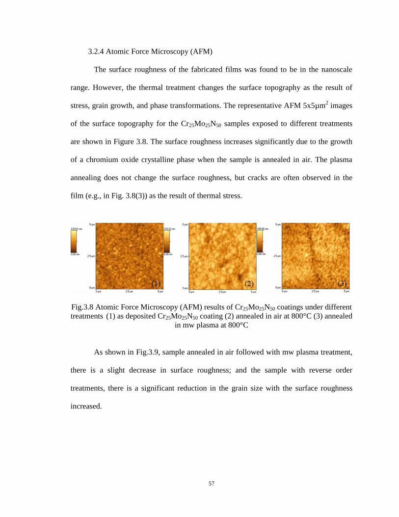
57
3.2.4 Atomic Force Microscopy (AFM)
The surface roughness of the fabricated films was found to be in the nanoscale
range. However, the thermal treatment changes the surface topography as the result of
stress, grain growth, and phase transformations. The representative AFM 5x5µm2 images
of the surface topography for the Cr25Mo25N50 samples exposed to different treatments
are shown in Figure 3.8. The surface roughness increases significantly due to the growth
of a chromium oxide crystalline phase when the sample is annealed in air. The plasma
annealing does not change the surface roughness, but cracks are often observed in the
film (e.g., in Fig. 3.8(3)) as the result of thermal stress.
Fig.3.8 Atomic Force Microscopy (AFM) results of Cr25Mo25N50 coatings under different
treatments (1) as deposited Cr25Mo25N50 coating (2) annealed in air at 800°C (3) annealed
in mw plasma at 800°C
As shown in Fig.3.9, sample annealed in air followed with mw plasma treatment,
there is a slight decrease in surface roughness; and the sample with reverse order
treatments, there is a significant reduction in the grain size with the surface roughness
increased.

58
Fig.3.9 AFM picture of (4) annealed in air at 600°C+in mw plasma (5) annealed in mw
plasma +in air at 800°C
3.3 Mechanical properties
3.3.1 Nanoindentation
The results of nanoindentation tests are shown in Fig.3.10. The measurements
were conducted by 10 times and taken the average value. It shows that the hardness of the
original sample is relatively low, about 9 GPa. However, thermal processing resulted in
significant changes in both the hardness and the Young’s modulus of the samples. The
sample annealed in the air at 800°C showed an increase in the hardness by 50%.
Unfortunately, this sample also shows an increase in surface roughness. For the
microwave plasma annealed sample, the surface roughness was comparable to the
untreated sample. However, the hardness only showed a modest increase of about 20%.

59
Fig3.10 Mechanical properties of (1) as deposited CrMoN coating (2) annealed in air at
800°C (3) annealed in mw plasma at 800°C (4) annealed in air at 600°C+in mw plasma
(5) annealed in mw plasma +in air at 800°C
In Table 3.2, we can see representative mechanical results of the two thermal
treatments in comparison with the untreated sample. From this, we can see the modulus
of the air annealed sample increased about 33% with respect to the untreated sample. The
modulus of the plasma annealed sample shows no significant change with respect to the
untreated sample. Following the discussion above, a combinatorial post-deposition
processing was proposed as the pathway for further modification of the microstructure
and properties of the ternary CrMoN films; in addition, this approach may lead to a better
understanding of the observed phenomena.

60
Table 3.2 Mechanical properties and surface roughness overview of the CrMoN coatings
under various thermal processes
Treatment Hardness
(GPa)
Modulus
(GPa)
Roughness
(Ra)nm
Cracking
As deposited 9 200 11.1 No
air at 800ºC 15 280 20.3 No
mw plasma at 800ºC 11 190 12.0 Yes
air 600ºC+plasma 800°C 10 225 10.7 No
Plasma 800°C+air 800ºC 7 175 30.0 No
Conclusion:
Cr25Mo25N50 coatings were successfully deposited on CoCrMo-alloy substrates,
using RF reactive magnetron sputtering. These films were subjected to various thermal
treatments. There are no significant changes observed in the film properties for thermal
treatments in the air or argon up to 600 ºC. Films annealed in the air at 800 ºC, show the
oxidation, as confirmed with both XRD and XPS. The dominant phase is Cr2O3. The
thermal treated films show an increase in both hardness and Young’s modulus, but there
is a corresponding increase in grain size and surface roughness. Films treated in Argon at
800 ºC, show a smaller increase in hardness, with an increase in grain size and surface
roughness. However, films annealed in microwave plasma at 800ºC, in an H2/N2 gas
mixture, show a slight increase in the mechanical properties, but with a decrease in
surface roughness, and grain size. The drawback is the possibility of crack formation in

61
the film, due to increased thermal stress. In addition, this process leads to the formation
of a new, presumably ternary or quaternary, nanocrystalline phase. Furthermore, we
treated samples with a combinatorial thermal process to further understand the observed
trends. For films annealed in the air at 600ºC, with subsequent annealing in H2/N2
microwave plasma at 800ºC, there is a slight increase in the mechanical parameters of the
film, with a slight decrease in surface roughness. By reversing the order of thermal
treatments, we observe a significant reduction in the grain size. However, the resultant
mechanical properties are substantially declined, and the surface roughness increased.
The use of thermal treatments has been successfully demonstrated to control grain
size, surface morphology, and mechanical properties in Cr25Mo25N50 coatings on
CoCrMo substrates. These simple processing techniques may be used for further
improvement of the surface characteristics of nanocomposite coatings on biomedical
implants. However, further research is necessary to understand the underlying physical
processes involved. As a result, we plan to continue this research with various
compositions of Cr-Mo-N coatings, and a wider range of thermal treatments.

62
CHAPTER 4
Cr1-xMoxNy COATINGS ON Si SUBSTRATES
4.1 Samples preparation
4.1.1 Film deposition
CrMoN coatings are the potential coatings used in a wide range of applications
such as high speed cutting tools, drilling, bearing, and biomedical implants. Their
properties dependent on the composition are important to be studied. To avoid the
substrate effect on the coatings, standard and uniform Si wafers (100) were used as the
substrate.
Ternary Cr1-xMoxNy coatings were deposited on Si wafers (100) by using a dual
rf-magnetron sputtering system (Nordiko 3500-13.56MHz) with Cr and Mo targets and a
60/40 argon/nitrogen gas mixture at 6µbar working pressure. The distance between the
substrate and the centers of 100-mm diameter targets was fixed around 150 mm. Purities
of Cr and Mo targets were 99.9%, respectively. The N2 gas was injected near the substrate
holder. The sputtering target bias voltages were varied from -500 V to -900 V which
allowed to preparing the ternary layers with Cr/Mo ratios in the range from 1/3 to 3/1.
Binary CrN and MoN coatings were also prepared under similar conditions for
comparison. The binary films are deposited in about 6µbar with Ar2/N2 ratio of 80/20.
The residual pressure was in the range of 10-5
Pa before the introduction of the sputtering
gases argon and nitrogen. All films have a Cr under-layer (deposited for 10 min, at -900
V/ 500 W, in ~6 µbar of Ar). The deposition processes were approximately 3-hour long,

63
to achieve about the same thickness of up to 2 m of the deposited films.
For the first set of the coatings, which named as (a1),(b1),(c1),(d1),(e1), the
substrate temperature during the process did not exceed 200 oC. For the second set of
coatings, (a2),(b2),(c2),(d2),(e2), the heater was set at 5 A, 22 V, and the deposition
temperature is around 400°C. Table 4.1 below shows the list of all the as-deposited
coatings.
Table 4.1 Deposition parameters of the as-deposited Cr1-xMoxNy coatings on Si substrates
Films with target
composition
Deposition
Temp(°C)
%(N2/Ar) in
plasma
Cr target
voltage(V)
Mo target
voltage(V)
(a)CrN (a1) 200 (20/80) -900 0
(a2) 400
(b)Cr32Mo18N50 (b1) 200 (40/60) -900 -500
(b2) 400
(c)Cr25Mo25N50 (c1) 200 (40/60) -720 -780
(c2) 400
(d)Cr18Mo32N50 (d1) 200 (40/60) -500 -900
(d2) 400
(e)MoN (e1) 200 (20/80) 0 -900
(e2) 400
4.1.2 Thermal processing of films
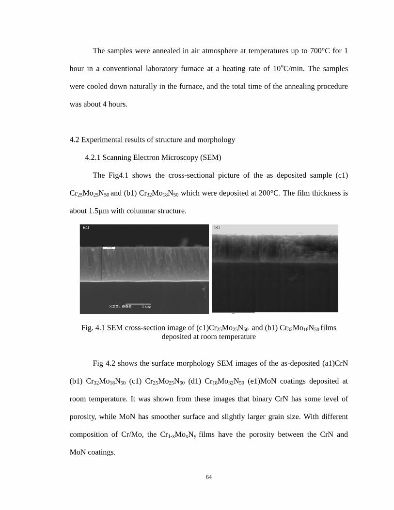
64
The samples were annealed in air atmosphere at temperatures up to 700°C for 1
hour in a conventional laboratory furnace at a heating rate of 10oC/min. The samples
were cooled down naturally in the furnace, and the total time of the annealing procedure
was about 4 hours.
4.2 Experimental results of structure and morphology
4.2.1 Scanning Electron Microscopy (SEM)
The Fig4.1 shows the cross-sectional picture of the as deposited sample (c1)
Cr25Mo25N50 and (b1) Cr32Mo18N50 which were deposited at 200°C. The film thickness is
about 1.5µm with columnar structure.
Fig. 4.1 SEM cross-section image of (c1)Cr25Mo25N50 and (b1) Cr32Mo18N50 films
deposited at room temperature
Fig 4.2 shows the surface morphology SEM images of the as-deposited (a1)CrN
(b1) Cr32Mo18N50 (c1) Cr25Mo25N50 (d1) Cr18Mo32N50 (e1)MoN coatings deposited at
room temperature. It was shown from these images that binary CrN has some level of
porosity, while MoN has smoother surface and slightly larger grain size. With different
composition of Cr/Mo, the Cr1-xMoxNy films have the porosity between the CrN and
MoN coatings.

65
Fig 4.2 The surface morphology SEM images of the as-deposited (a1)CrN (b1)
Cr32Mo18N50 (c1) Cr25Mo25N50 (d1) Cr18Mo32N50 (e1)MoN coatings deposited at room
temperature.
The Fig4.3 shows both the surface and cross-sectional morphology of as
deposited Cr1-xMoxNy coatings which were deposited at 400°C. From the cross-sectional
images, the ternary films (b2) (c2) (d2) show preferred oriented growth direction with
clear columnar structure, which can also be told from the surface morphology. There is
no great difference between the surface morphology of ternary films. However, the
binary films (a2) (e2) show much denser structure.
Fig. 4.3 Cross sectional and surface SEM pictures of (a2)CrN (b2)Cr32Mo18N50
(c2)Cr25Mo25N50 (d2)Cr18Mo32N50 (e2)MoN coatings deposited at 400°C
Fig. 4.4 shows the surface morphology of the coatings which deposited at 400°C
after annealing in air at 600°C. For the films deposited at 400°C, the surface morphology
of films (a2) (b2) (c2) (d2) didn't change after being annealed at air at 600°C for one hour.

66
However, the film (e2) MoN, is fully oxidized with the growth of oxidation, which can be
observed as a plate-like structure (oxidation) on the surface.
Fig. 4.5 shows the surface morphology of the 400°C deposited coatings after
annealing in air at 700°C. Only (a2)CrN (b2)Cr32Mo18N50 (c2)Cr25Mo25N50 coatings
survived without delamination after annealing in air at 700°C. It was suggested that there
was a growth of oxidation on the surface of (b2)Cr32Mo18N50 coating, and the (a2)CrN
and (c2) Cr25Mo25N50 were still with smooth surface.
Fig.4.4 SEM picture of (a2)CrN (b2)Cr32Mo18N50 (c2)Cr25Mo25N50 (d2)Cr18Mo32N50
(e2)MoN coatings deposited at 400°C after annealed in air at 600°C

67
Fig.4.5 SEM picture of (a2)CrN (b2)Cr32Mo18N50 (c2)Cr25Mo25N50 coatings annealed in
air at 700°C
4.2.2 X-Ray Diffraction (XRD)
Fig.4.6 shows X-ray diffraction patterns of Cr1-xMoxNy coatings at various Cr/Mo
ratios which were deposited at 200°C. We can see clearly in Fig.4.6 from the patterns that
for pure CrN(a1) and MoN(e1) coating, the patterns show preferred orientations of (111)
and (200) crystal planes of face-centered-cubic (fcc) CrN, Mo2N crystal structure,
respectively. As the Mo content in the Cr1-xMoxNy coatings increased, the diffraction
peaks were gradually shifted from those of pure CrN coating to those lower angle
diffraction of pure MoN coating, reveals larger lattice parameters which will be shown
later. From Scherrer equation, we can calculate that the mean grain size of the coatings is
13-21 nm.

68
Fig.4.6 XRD patterns of as deposited (a1)CrN (b1)Cr32Mo18N50 (c1)Cr25Mo25N50
(d1)Cr18Mo32N50 (e1)MoN deposited at room temperature
Fig.4.7 and Fig.4.8 show the XRD patterns of these Cr1-xMoxNy (deposition
temperature 200°C) annealed at 600 oC and 700
oC, respectively. The MoN coating was
completely oxidized after annealing in air at 600 °C for one hour, and ternary
Cr18Mo32N50 coating (d), which had a higher Mo content, also oxidized and delaminated
after annealing in air at 700°C, whereas the ternary Cr32Mo18N50 coating (b1), with
Cr/Mo ratio more than 1.7, survived at 700 °C without cracking or delamination. Based
on the XRD peaks positions in Fig.4.6 and Fig.4.7, it is indicated that Cr2O3 is the main
crystalline phase after annealing process.

69
Fig.4.7 XRD patterns of (a1)CrN (b1)Cr32Mo18N50 (c1)Cr25Mo25N50 (d1)Cr18Mo32N50
(e1)MoN deposited at room temperature after annealed at air at 600°C
Fig.4.8 XRD patterns of (a1)CrN (b1)Cr32Mo18N50 (c1)Cr25Mo25N50 deposited at room
temperature after annealed at air at 700°C

70
For the films deposited at 400°C, the XRD patterns illustrated the difference on
the phase transformation.
Fig.4.9 XRD patterns of (a2)CrN as deposited at 400°C and under thermal processes
For the pure (a2)CrN (Fig.4.9), the effect of deposition temperature on phase
formation was found that with higher deposition temperature, the films consist of
primarily fcc CrN phase and with hexagonal h-Cr2N phase. With low deposition
temperature, the deposition results in films of nearly stoichiometric CrN and the films
71
show strong (111) type texture. It is reasonable that the formation the hexagonal Cr2N
phase has a much narrower window than the formation of fcc CrN phase. During
oxidation of Cr2N a transformation into CrN was observed as shown in Fig.4.8 that as the
increase of the annealing temperature, the hexagonal Cr2N phase disappeared, and with
the enhancement of the fcc CrN (111) peak. (a2)CrN had no oxidation when annealed at
600°C, and started to have small oxidation at 700°C.
For the (a2)MoN (Fig.4.10), face-centered cubic phases (γ-Mo2N) were formed
with pronounced (111) direction growth. However, a secondary phase precipitate was
observed at the left side of the (111) peak. This secondary phase didn't change after
thermal treatments. The resistance of Mo–N coatings to oxidation is poor because of their
non-protective nature and the volatility of the oxides at moderately high temperatures. At
annealing temperature 400°C, the (a2)MoN films were oxidized with the main oxidation
product of MoO3, which were also responded to the SEM results.

72
Fig.4.10 XRD patterns of (e)MoN as deposited at 400°C and under thermal processes
For the ternary Cr18Mo32N50 coating (d2) which contains more Mo (Fig.4.10),
survived at 600°C annealing temperature, but oxidized and delaminated after annealing in
air at 700°C.

73
Fig.4.11 XRD patterns of (d2)Cr18Mo32N50 as deposited at 400°C and under thermal
processes
Whereas the ternary Cr32Mo18N50 coating (b2) (Fig.4.12) and (c2)Cr25Mo25N50
(Fig.4.13), with higher Cr/Mo ratio, survived at 700 °C without cracking or delamination.
This behavior followed the same trend as we got from the films deposited at 200°C. It
should be mentioned that, secondary phase precipitates were observed both in (c2) and
(d2). This was not observed at the first set of samples which were deposited at lower
temperature. It relies on changes in solid solubility with temperature to produce fine

74
particles of an impurity phase, which impede the movement of dislocations, or defects in
a crystal's lattice. This may lead to better thermal stability and mechanical properties.
Fig.4.12 XRD patterns of (b2)Cr32Mo18N50 as deposited at 400°C and under thermal
processes
Compare the XRD patterns of (c1) and (c2) which were with the same
composition of Cr/Mo, but with different deposition temperature, both of the films
survived at annealing temperature 700°C, the (c1) coating which deposited at room
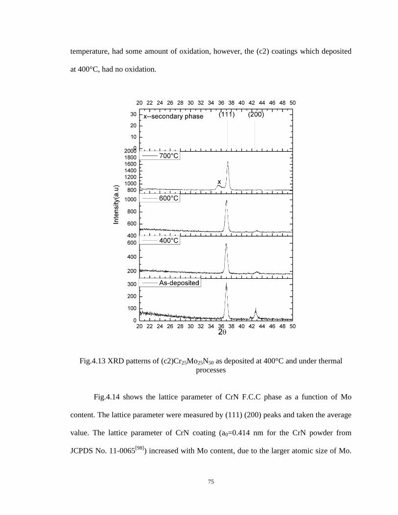
75
temperature, had some amount of oxidation, however, the (c2) coatings which deposited
at 400°C, had no oxidation.
Fig.4.13 XRD patterns of (c2)Cr25Mo25N50 as deposited at 400°C and under thermal
processes
Fig.4.14 shows the lattice parameter of CrN F.C.C phase as a function of Mo
content. The lattice parameter were measured by (111) (200) peaks and taken the average
value. The lattice parameter of CrN coating (a0=0.414 nm for the CrN powder from
JCPDS No. 11-0065[98]
) increased with Mo content, due to the larger atomic size of Mo.

76
The peak shift phenomenon due to Mo addition toward lower angle reflects that the Cr-
Mo-N coatings were substitutional solid solutions of (Cr,Mo)N. This will be discussed in
the discussion chapter 5. The difference in lattice parameters of the coatings deposited at
different temperature resulted from the selection of (111) or (200) peak, for the reason
that for the coatings deposited at 400°C, there are combination of fcc and hexagonal
phase, and the fcc (111) peak are not pronounced.
Fig. 4.14 Lattice parameters CrxN and MoxN selected (111) or (200) crystal plane as a
function of Mo content
The thermal stability of the coatings was found to increase with a larger amount
of Cr in the ternary system.
4.2.3 Transmission Electron Microscopy (TEM)
Due to the facility limitation, only the (c1) Cr25Mo25N50 was taken with TEM high
magnification picture. As showed in Fig.4.15, the clear columnar structure was observed.

77
Also on the surface, a typical area was shown in here, with clear interplannar distances
correspond to those measured by XRD.
Fig.4.15 TEM high magnification cross-sectional and surface morphology of (c1)
Cr25Mo25N50 coatings deposited at room temperature
4.2.4 X-ray Photoelectron Spectroscopy (XPS)
The XPS data characterize a very thin layer (2-4 nm). According to the XPS data
of the first set of samples as shown in Fig.4.16 (deposition temperature 200°C), the
surface layer of (a1)CrN sample after 4 keV Ar+ ion-beam sputtering consists of 74 at. %
Cr, 17 at. % N, 5 at % C, and 4 at % O. The Cr2p peaks are deconvoluted into two

78
distinct states; the Cr2p3/2
peaks are located at 571.4 eV and 575.9 eV. The N1s peak is
also in two states at 396.5 eV and 397.5 eV. While not shown, the C1s is in two states,
with a weak peak centered at 282.3 eV and much stronger peak at 284.7 eV. The O1s has
a strong peak at 530.7 eV, with a much weaker peak at 532.2 eV. This information
implies that the sample is mainly composed of two Cr-N bonds (probably, in Cr2N and
CrN phase), with small, but detectable amounts of Cr-O, Cr-C, and C-C bonds. Similarly,
the MoxN sample deconvoluted into several Mo-N bond states, with some portion
assigned to Mo-O, Mo-C, and C-C bonding. Fig. 4.16 only shows representative XPS
data for (a1)CrN, (c1)Cr25Mo25N50, and (e1)MoN coatings.
For the (d1)Cr18Mo32N50 sample, there were only 7 at.% Cr, 63 at.% Mo, 27 at.%
N, 1 at.% C, and 2 at.% O, according to XPS measurements. Looking more closely at the
high resolution spectra, the Cr2p peaks deconvoluted into two distinct states, with 2p3/2
peaks at 574.9 eV and 575.8 eV. Unfortunately, the Mo3p3/2
and N1s peaks overlap with
two peaks located at 394 eV and 397 eV, respectively. Using standard references [PHI,
NIST], the peak at 397 eV is most likely due to a Mo-N bonding state of N1s level, and
the 394 eV peak is tied to Mo-N state in Mo3p3/2
energy level. In addition, the Mo3d
spectra deconvolute into three peaks at 228.3 eV, 230 eV, and 232.7 eV. Finally, the O1s
state has two peaks at 529.6 eV and 531.6 eV, and C1s is in one state at 284.7 eV. From
this complex picture, the bonding structure of Cr18Mo32N50 sample emerges as mostly
Mo-N with Cr-N inclusions, and small amounts of metal oxides and C-C bonds.

79
Fig.4.16 XPS results of (a1)CrN (c1) Cr25Mo25N50 (e1)MoN coatings deposited at room
temperature
Interestingly, the shapes and positions of Mo3d and Cr2p peaks (see Fig.4.16 for
the examples) were almost the same through the entire range of the ternary Cr1-xMoxNy
compositions. The major differences were observed in the positions of N1s and Mo3p3/2
levels. First, the intensity of N1s peak at 397.4 increases with the increase of Cr content.

80
However, the position of this peak does not change in all ternary compositions. The N1s
peak is located at 396.5 eV in binary CrN film. The Mo3p3/2
level in Cr1-xMoxNy shifts
from 393.8 for binary MoN to 394.3 with the increase of Cr content.
For the Cr-rich (b1)Cr32Mo18N50 sample, there were 34 at. % Cr, 27 at. % Mo, 33
at. % N, 3 at. % C, and 3 at. % O according to XPS. The Cr2p peaks deconvolute into
two states, with the 2p3/2
peaks at 574.2 eV and 574.6 eV. The spectra containing the
Mo3p3/2
and N1s states have two peaks at 394.3 eV and 397.4 eV. Following the same
arguments from the prior sample, these states are most likely a nitride and Mo-N bonds.
The Mo3d consists of two states at 228.3 eV and 231.6 eV. O1s has two peaks at 530.2
eV and 531.1 eV; C1s shows two peaks at 284.7 eV and 288.94 eV. The most likely
bonding structure is similar to the Cr18Mo32N50 sample. There is mainly Mo-N with Cr-N
inclusions, and detectable amounts of metal oxides, carbonate, and C-C bonds.
The last sample, Cr25Mo25N50(c1), consists of 24 at. % Cr, 35 at. % Mo, 38 at. %
N, 2 at. % C, and 2 at. % O as XPS shows. Once again, the Cr2p deconvolutes into two
states, with 2p3/2
peaks at 574.2 eV and 574.4 eV. The Mo3p3/2
spectra break down into
two peaks at 394.1 eV and 397.4 eV. Peaks located at 228.2 eV and 231.4 eV make up
the Mo3d spectra. O1s consists of 529.7 eV and 530.4 eV peaks. For C1s, there are
peaks at 283 eV, 285.1 eV, 289.8 eV, and 291.5 eV. Again, there is a very similar
bonding structure; the sample appears to be Cr-N inclusions within a matrix of Mo-N.
There are some small amount of metal oxide, carbonate, and C-C bonds.
Fig. 4.17 shows the bonding stage of the CrMoN coatings deposited at 400°C.
The samples deposited at higher temperature, generally the evolution of the chemical
bonding is very similar to those of with lower deposition temperature. For example, in

81
(a2)CrN, the Cr2p peaks are deconvoluted into two distinct states which suggested there
were two Cr-N bonds (probably, in Cr2N and CrN phase), this is correspond to the XRD
results. For the films contained Mo, the N1s peak overlapped with the Mo3p peaks at
394eV. All films are with small, but detectable amounts of Cr-O, Cr-C, and C-C bonds.
Fig.4.17 XPS results of as deposited (a2)CrN (b2)Cr32Mo18N50 (c2)Cr25Mo25N50
(d2)Cr18Mo32N50 (e2)MoN coatings deposited at 400°C
Overall, based on the XRD and XPS data, it is possible that the ternary Cr1-
xMoxNy material in these experiments is a true solid solution, and no phase segregation,
needed for the nanocomposite formation, is observed. A relatively low substrate
temperature during the deposition may be a factor. Indeed, the decomposition of such
Cr25Mo25N50 ternary phase into two nanocrystalline phases (CrN-rich and MoN-rich) was
observed at above 800 oC in non-oxidizing atmosphere.
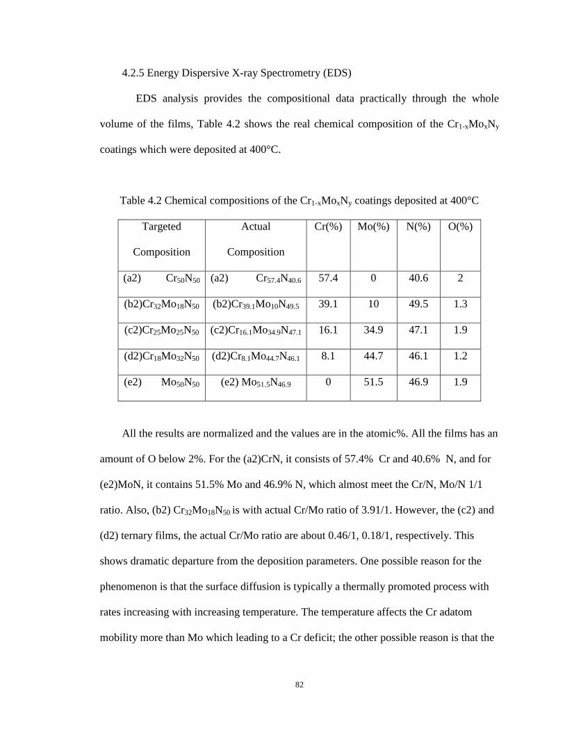
82
4.2.5 Energy Dispersive X-ray Spectrometry (EDS)
EDS analysis provides the compositional data practically through the whole
volume of the films, Table 4.2 shows the real chemical composition of the Cr1-xMoxNy
coatings which were deposited at 400°C.
Table 4.2 Chemical compositions of the Cr1-xMoxNy coatings deposited at 400°C
Targeted
Composition
Actual
Composition
Cr(%) Mo(%) N(%) O(%)
(a2) Cr50N50 (a2) Cr57.4N40.6 57.4 0 40.6 2
(b2)Cr32Mo18N50 (b2)Cr39.1Mo10N49.5 39.1 10 49.5 1.3
(c2)Cr25Mo25N50 (c2)Cr16.1Mo34.9N47.1 16.1 34.9 47.1 1.9
(d2)Cr18Mo32N50 (d2)Cr8.1Mo44.7N46.1 8.1 44.7 46.1 1.2
(e2) Mo50N50 (e2) Mo51.5N46.9 0 51.5 46.9 1.9
All the results are normalized and the values are in the atomic%. All the films has an
amount of O below 2%. For the (a2)CrN, it consists of 57.4% Cr and 40.6% N, and for
(e2)MoN, it contains 51.5% Mo and 46.9% N, which almost meet the Cr/N, Mo/N 1/1
ratio. Also, (b2) Cr32Mo18N50 is with actual Cr/Mo ratio of 3.91/1. However, the (c2) and
(d2) ternary films, the actual Cr/Mo ratio are about 0.46/1, 0.18/1, respectively. This
shows dramatic departure from the deposition parameters. One possible reason for the
phenomenon is that the surface diffusion is typically a thermally promoted process with
rates increasing with increasing temperature. The temperature affects the Cr adatom
mobility more than Mo which leading to a Cr deficit; the other possible reason is that the

83
confocal arrangement of the Cr and Mo guns cross-talked during the deposition, led to
the non-uniformed composition.
4.2.6 Stress
The elliptical curvature was observed with the profilometer, and after applied to
the Stoney formula, the stress in the films which were deposited at 400°C, was listed in
the Table.4.3. All these films show low stress. The binary (a2)CrN shows tensile stress of
1.23 GPa and (e2)MoN shows the compressive stress of -1.01 GPa, this due to the
thermal expansion coefficient difference among the Cr, Mo and the Si substrate. As the
simple combination principle, the lower stresses in the ternary films were obtained. The
stress of targeted compositional (b2) Cr32Mo18N50 (c2) Cr50Mo50N50 (d2) Cr18Mo32N50 are
0.41GPa, 0.64 GPa, and 0.48 GPa, respectively. The initial stress in the films could
improve the mechanical properties of the film at some level.
Table 4.3 Residual stresses in the Cr1-xMoxNy coatings deposited at 400°C
Sample Stress (GPa)
(a2) Cr57.4N40.6 1.23
(b2)Cr39.1Mo10N49.5 0.41
(c2)Cr16.1Mo34.9N47.1 0.64
(d2)Cr8.1Mo44.7N46.1 0.48
(e2) Mo51.5N46.9 -1.01

84
4.2.7 Atomic Force Microscopy (AFM)
All the deposited films were well adherent to Si substrate and exhibited smooth
surface with the roughness in a sub-10 nm range. Fig.4.18 shows the AFM 2.5μm x
2.5μm images of Cr1-xMoxNy films deposited at room temperature.
Fig.4.18 AFM images of (a1)CrN (b1)Cr32Mo18N50 (c1)Cr25Mo25N50 (d1)Cr18Mo32N50
(e1)MoN coatings deposited at room temperature
From these images and compare with the SEM images shown before, it was
suggested that binary CrN has some level of porosity which results in its higher
roughness and lower hardness in nanoindentation tests, while MoN has smoother surface
and slightly larger grain size. With different composition of Cr/Mo, the Cr1-xMoxNy films
have the properties between the CrN and MoN coatings. We believe that Cr32Mo18N50
coating (b1), which contains more Cr, still has many pores which results in a relatively
higher roughness. As the Mo content increased from (c1) Cr25Mo25N50 to (d1)
Cr18Mo32N50, the surface becomes smoother.
The thermal processing has been found to reduce roughness of the films that
survived the corresponding temperatures (Fig.4.19). This could be the result of the
reduction of porosity in Cr-rich films due to the oxide growth. The surface grain growth
seems to occur as seen in AFM images, which can be related to the partially amorphous
oxide layer formation. While not shown, several initial tests at higher temperatures
inevitably led to the increased roughness.
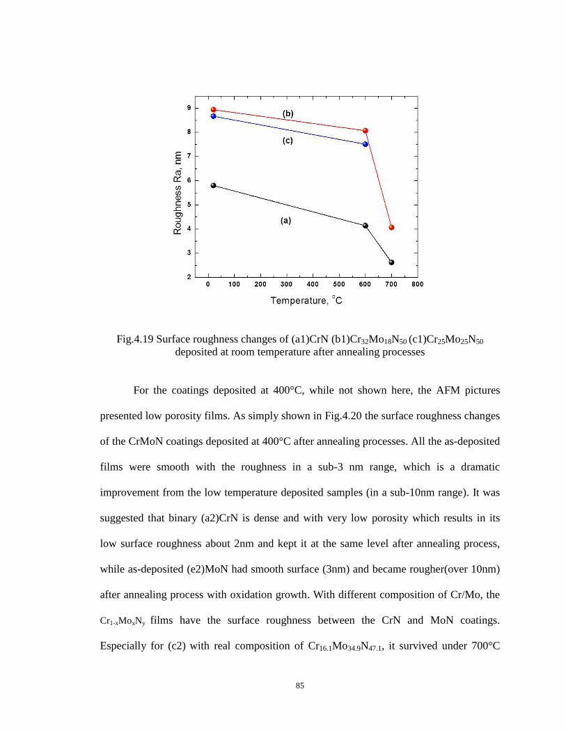
85
Fig.4.19 Surface roughness changes of (a1)CrN (b1)Cr32Mo18N50 (c1)Cr25Mo25N50
deposited at room temperature after annealing processes
For the coatings deposited at 400°C, while not shown here, the AFM pictures
presented low porosity films. As simply shown in Fig.4.20 the surface roughness changes
of the CrMoN coatings deposited at 400°C after annealing processes. All the as-deposited
films were smooth with the roughness in a sub-3 nm range, which is a dramatic
improvement from the low temperature deposited samples (in a sub-10nm range). It was
suggested that binary (a2)CrN is dense and with very low porosity which results in its
low surface roughness about 2nm and kept it at the same level after annealing process,
while as-deposited (e2)MoN had smooth surface (3nm) and became rougher(over 10nm)
after annealing process with oxidation growth. With different composition of Cr/Mo, the
Cr1-xMoxNy films have the surface roughness between the CrN and MoN coatings.
Especially for (c2) with real composition of Cr16.1Mo34.9N47.1, it survived under 700°C

86
annealing and still with surface roughness in the sub-4nm.
Fig. 4.20 Surface roughness changes of (a2)CrN (b2)Cr32Mo18N50 (c2)Cr25Mo25N50
(d2)Cr18Mo32N50 (e2)MoN coatings deposited at 400°C after annealing processes
4.3 Mechanical properties
4.3.1 Nanoindentation
Fig.4.21 shows the nanoindentation hardness and modulus value of Cr1-xMoxNy
films at low deposited temperature. The binary (a1)CrN coating has a hardness of 9 GPa,
whereas the binary (e1)MoN coating has a higher hardness at 15 GPa. The CrMoN
coatings have the hardness value between CrN and MoN coatings. The elastic modulus
qualitatively follows the evolution of the hardness. All the samples show an increase in
the hardness and modulus after the annealing below the delamination or severe oxidation

87
(i.e., MoN) thresholds. The hardness of (a1)CrN coating increased by about 40% and its
modulus increased about 50% after annealing at 600 oC, and the Cr1-xMoxNy coatings with
higher Cr content also showed a noticeable increase both in hardness and modulus. The
hardness of (b1)Cr32Mo18N50 film increased by about 20% and for (c1)Cr25Mo25N50 it
increased by about 30%. The increase of hardness after thermal treatment may due to the
reduction of porosity by the oxidation (rule of mixtures) of the coating. However, the
partial phase segregation cannot also be ruled out.
Fig.4.21 Hardness and Young’s Modulus changes of (a1)CrN (b1)Cr32Mo18N50
(c1)Cr25Mo25N50 (d1)Cr18Mo32N50 (e1)MoN coatings after annealing processes
For the coatings deposited at higher temperature (400°C), the mechanical
properties have been dramatically improved. The elastic modulus qualitatively follows
the evolution of the hardness. As shown in Fig.4.22, The binary (a2)CrN coating has a
hardness of 18 GPa, compared to the (a1)CrN, the hardness doubled with the increase of
the deposition temperature. The binary (e2)MoN coating has a higher hardness at 22GPa
compared to (e1) MoN at15 GPa. The (b2)(c2)(d2) CrMoN coatings have the hardness
value between (a2)CrN and (e2)MoN coatings, however, only have a slightly increase in
the hardness in comparison with the first set which were deposited at room temperature,

88
are still not desired. These results were indicated by the SEM cross-section pictures that
the binary films are much denser than the ternary films (columnar structure).
Fig.4.22 Hardness and Young’s Modulus of (a2)CrN (b2)Cr32Mo18N50 (c2)Cr25Mo25N50
(d2)Cr18Mo32N50 (e2)MoN coatings deposited at 400°C
Fig.4.23 shows the hardness changes of the CrMoN coatings deposited at 400°C
after annealing processes. For the samples after the annealing process at 600°C, (a2)CrN,
(b2) Cr32Mo18N50 and (c2)Cr25Mo25N50 show an increase in the hardness and modulus.
As the growth of the oxidation when the annealing temperature increased to 700°C, the
hardness of (a2)CrN and (b2)Cr32Mo18N50 film decreased by about 30%. It is very
promising that for (c2) Cr25Mo25N50 , the hardness increased nearly by linearly under the
thermal processes (Fig.4.22).

89
Fig.4.23 Hardness and Young’s Modulus changes of (a)CrN (b)Cr32Mo18N50
(c)Cr25Mo25N50 coatings deposited at 400°C after thermal processes
As discussed above, the mechanical properties of the ternary Cr1-xMoxNy coatings
are the critical issue for achieving the desired coatings, in order to overcome the defects
such as boundary defects and dislocation, two multilayer samples were prepared at
similar conditions with a layer periodicity of 10nm and 25nm, respectively. Table 4.4
shows the deposition parameters of the multilayer CrN/MoN coatings and comparison
with the Cr25Mo25N50 coatings which were deposited at room temperature and 400°C.

90
Table 4.4 Deposition parameters of multilayer coatings CrN/MoN (m1),(m2) and single
layer Cr25Mo25N50 coatings deposited at room temperature (c1) and high temperature (c2)
Sample Deposition
temperature
Layer
periodicity
(nm)
Layers Film
thickness(µm)
Cr
Bias
(V)
Mo
Bias
(V)
(m1)CrN/MoN 400°C 10 100 2 -900 -900
(m2)CrN/MoN 400°C 25 40 2 -600 -600
(c1)Cr25Mo25N50 200°C 1.5 -720 -780
(c2)Cr25Mo25N50 400°C 2.5 -720 -780
Fig 4.24 Cross-sectional SEM images of multilayer CrN/MoN (m1) and (m2)
coatings
Fig. 4.24 shows the cross-sectional image of the multilayer CrN/MoN coatings.
The layer structure is composed of two materials CrN, which is darker layer in the cross-
sectional image, and MoN, which is lighter layer presented. The Mo layers are thicker
than as expected, this corresponds to the EDS result of the chemical composition of the
single layer Cr25Mo25N50 coatings, which also presented higher Mo content.

91
Fig. 4.25 gives the surface morphology SEM images and AFM images. The
multilayer (m1) with thinner layer shows smoother surface with surface roughness of
3.6nm, whereas the multilayer (m2) with thicker layer shows a surface roughness of
7.4nm. Compared with the single layer (c2) Cr25Mo25N50 coating, the multilayer (m1)
Cr/MoN had the competitive surface roughness ((c2) Cr25Mo25N50 with surface roughness
of 3.3nm).
Fig. 4.25 Surface morphology SEM and AFM images showing the surface roughness of
multilayer CrN/MoN coatings
The nanoindentation test found the mechanical properties has been greatly
improved by multilayer (m1) CrN/MoN which contained thinner layers of 10nm, with
hardness of 21 GPa and Modulus of 310 GPa which is shown in Fig. 4.26.

92
Fig. 4.26 Mechanical properties of multilayer CrN/MoN coatings compared with the
Cr25Mo25N50 coatings
The multilayer CrN/MoN coating with thinner layer periodicity gives better
mechanical properties than that with thicker layer periodicity and those of the single
layers CrMoN coatings, which is due to the superlattice structure in the multilayer
coatings greatly improved the lattice deficit, dislocations, grain boundaries, etc.
4.3.2 Tribology
Fig.4.27 shows the average friction coefficient of Cr1-xMoxNy coatings with
various Mo contents (x value) which were deposited at 200°C against Ti ball. The
average coefficient of friction of CrN was at a value of 0.55, while the lower value of
0.41 was obtained in MoN film. This results is explained by the tribo-chemical reaction,
where the coating layer reacts with ambient H2O to form the MoO3 thin layer during
sliding process. The MoO3 layer can function as a solid lubricant to reduce direct contact

93
between the coating surface and Ti ball [99,100,101,102]
. The COF of ternary coatings are in
the range of between binary CrN and MoN coatings.
While wasn't shown here, with the increase of normal load, the coefficient of
friction decreases slightly, which can probably be explained by wear debris and
generating of lubricating surface layer with the increase of normal load. The long term
coefficient of friction remains a stable value.
Fig.4.27 Coefficient of Friction (COF) of Cr1-xMoxNy coatings deposited at 200 °C
As shown in Fig. 4.28, for the coatings deposited at 400°C, the COF of as-
deposited films behavior very similar to the coatings deposited at 200°C, decreased from
0.65 for CrN to 0.42 for MoN. The coating with Cr/Mo targeted ratio of 1/1 has the
lowest COF among the ternary films. After the coatings were annealed in air atmosphere
at 600°C and 700°C, the COF remains stable under the oxidation and delamination
threshold.

94
Fig.4.28 Coefficient of Friction (COF) of Cr1-xMoxNy coatings deposited at 400 °C
Conclusion:
Ternary chromium molybdenum nitride Cr1-xMoxNy films coatings were deposited on
silicon wafers by using a dual rf-magnetron sputtering system. While all films had low
roughness and were highly adherent to Si substrate, with lower roughness observed in the
films which were deposited at higher temperature. The overall properties of the coatings
deposited at higher temperature were improved compared with the coatings deposited at

95
room temperature. Table 4.5 shows the selected properties overview of the samples
deposited at 400°C.
Table 4.5 Selected properties overview of the Cr-Mo-N coatings deposited at 400°C
Films with real
composition
Delamination
/Cracking
@600°C
Hardness
increase
@600°C
Smooth
surface
@600°C
Delamination/
Cracking
@700°C
Hardness
increase
@700°C
Smooth
surface
@700°C
(a2)Cr57.4N40.6 NO YES YES NO NO YES
(b2)Cr39.1Mo10N49.5 NO YES YES NO NO NO
(c2)Cr16.1Mo34.9N47.1 NO YES YES NO YES YES
(d2)Cr8.1Mo44.7N46.1 NO NO YES YES NO NO
(e2)Mo51.5N46.9 YES NO NO YES NO NO
Only Cr-rich materials with the Cr/ Mo ratio of more than 16.9/34.9 were able to
withstand thermal treatment in air up to 700 oC. The MoN and Mo-rich ternary films
were completely oxidized and delaminated after annealing in air at 600 °C and 700°C for
one hour. The hardness of the films was below the expectation and this was assigned to
the porosity of Cr-containing films. However, Cr-rich films thermally processed at up to
600 oC show an increase both in hardness and Young’s modulus. The hardness of Cr1-
xMoxNy coatings which with Cr/Mo ratio of more than 3.91 increased by about 20% after
annealing, at the same time, the surface roughness of the films was reduced. Desired
mechanical properties were achieved in binary CrN and MoN films deposited at higher
temperature (400°C). Although the desired mechanical properties were not reached in

96
ternary films, the adjustment of Cr/Mo ratio during the deposition process allows to
obtaining ternary Cr1-xMoxNy coatings with the properties between those of binary CrN
and MoN.

97
CHAPTER 5
DISCUSSION AND CONCLUSION
For the low temperature deposition, all the films contain a single fcc phase. For
the high temperature deposition, the ternary films crystallize in mainly F.C.C phase with
a strong texture in the (111) direction. The molybdenum nitride films contain mainly the
γ-Mo2N phase and the chromium nitride films crystallize in the fcc CrN and hexagonal
Cr2N phase. The phase formation difference is probably due to the rephrase from the
deposition temperature. The phase transformation can be further discussed with reference
to the phase diagram of the Cr-Mo-N system, which is given in Fig. 5.1.
Fig. 5.1 Chromium-Molybdenum-Nitrogen ternary alloy phase diagram(based on 1991
Frisk K.)103

98
The formation of hexagonal Cr2N has a much narrow window of condition
compared to the formation of F.C.C CrN. Increasing the deposition temperature leads to
densification of porous column boundaries, defect incorporation, and enhanced
renucleation rate from ion bombardment-induced surface defects leading to a suppression
of the columnar-type growth. These high-energy ions effectively bombard the growing
film and a densely packed morphology results. The hardness increases in CrN system if
the content of the hexagonal phase increases. While the crystallites of all coatings consist
of crystallites of up to 23 nm. Apart from the crystal size, the morphology does not
change significantly for all films over the whole parameter range of this study.
Nanoindentation measurements revealed a maximum hardness value of about 22
GPa observed in MoN film, while the films with about equal amounts of chromium and
molybdenum appear to be softer ~hardness values in 11 GPa. The chromium nitride thin
films show hardness values of 18 GPa, which are significantly higher in comparison with
those of CrN deposited at lower temperature. Tensile stresses up to 1.23 GPa were
measured for the binary film, while the ternary films exhibit tensile stresses in lower
range. The values for the elastic modulus were in the range of 330 (MoN) and 185 GPa
(Cr18Mo32N50). The different hardness values of the binary and the ternary films are
mainly due to changes in the bonding character. Also, softening may caused by the grain
boundary sliding which is mainly attributed to the large amount of defects in the grain
boundaries that allows fast diffusion of atoms and vacancies with the applying of stress.
A solid solution is formed when two metals are completely soluble in liquid state
and also completely soluble in solid state. In other words, when homogeneous mixtures
of two or more kinds of atoms (of metals) occur in the solid state, they are known as solid

99
solutions. The more abundant atomic form is referred as solvent and the less abundant
atomic form is referred as solute104
. If the atoms of the solvent or parent metals are
replaced in the crystal lattice by atoms of the solute metal then the solid solution is
known as substitutional solid solution.
Hume Rothery formulated certain rules which govern the formation of
substitutional solid solutions. These are:
(a) Crystal structure factor: For complete solid solubility, the two elements should have
the same type of crystal structure i.e., both elements should have either F.C.C. or B.C.C.
or H.C.P. structure.
(b) Relative size factor: As the size (atomic radii) difference between two elements
increases, the solid solubility becomes more restricted. For extensive solid solubility the
difference in atomic radii of two elements should be less than about 15 percent. If the
relative size factor is more than 15 percent, solid solubility is limited. For example, both
silver and lead have F.C.C. structure and the relative size factor is about 20 percent.
Therefore the solubility of lead in solid silver is about 1.5 percent and the solubility of
silver in solid lead is about 0.1 percent. Copper and nickel are completely soluble in each
other in all proportions. They have the same type of crystal structure (F.C.C.) and differ
in atomic radii by about 2 percent.
(c) Chemical affinity factor: Solid solubility is favored when the two metals have lesser
chemical affinity. If the chemical affinity of the two metals is greater than greater is the
tendency towards compound formation. Generally, if the two metals are separated in the
periodic table widely then they possess greater chemical affinity and are very likely to
form some type of compound instead of solid solution.

100
(d) Relative valence factor: It is found that a metal of lower valence tends to dissolve
more of a metal of higher valence than vice versa. For example in aluminum-nickel alloy
system, nickel (lower valance) dissolves 5 percent aluminum but aluminum (higher
valence) dissolves only 0.04 percent nickel.
In the sputtered ternary Cr1-xMoxNy films, the Cr and the Mo atoms are randomly
distributed over the metal sublattice. CrN and MoN both have F.C.C structures, Mo
atoms may substitute for Cr atoms without disturbing the F.C.C structure of CrN, which
was shown in the XRD results. The films still have some secondary phase precipitates
due to the solid solubility of these two materials. The octahedral coordination can be
deformed, leading to local modifications of the covalent/ionic bonds between metal and
nitrogen atoms. Consequently, the charge distribution and covalence level of these bonds
are changed. Additionally, due to the distorted lattice (molybdenum) has larger covalent
and ionic radii compared to chromium, and nitrogen vacancies, metallic bonds are
reinforced [105,106]
. The number of metal–nitrogen bonds with covalent/ionic character is
diminished.
In conclusion, the adjustment of Cr/Mo ratio during the deposition process allows
to obtaining ternary Cr1-xMoxNy coatings with the properties between those of binary CrN
and MoN. Good thermal stability, low surface roughness and tribological properties have
been achieved by the desired Cr/Mo ratio of 16.1/34.9.
The mechanical properties were significantly improved by the multilayer CrN/MoN
coatings, and the surface roughness were comparable to those of the monolayer Cr-Mo-N
coatings. Further investigation of the multilayer CrN/MoN coatings, such as the thermal
stability and oxidation resistance, need to be conducted. The complex structure can show

101
advantages in the mechanical properties due to the overcome of the boundary defects and
dislocations. However, for the specific cutting tool application, whether multilayer
coating designs are really advantageous regarding the cutting performance will have to be
evaluated for each application. For example, the multilayer structured TiN/TiCN coatings
had negative effects on the cutting performance of cemented carbides, such as the
reduction of the thermal conductivity and a decrease of the resistance against abrasive
wear.107
It seems that for cutting operations with a high load of tribo-oxidation of the
multilayer coatings with oxide top layers have a high potential. The optimization of the
process to improve the mechanical properties with high thermal stability is the obvious
next step for the multilayer CrN/MoN coatings.

102
LIST OF REFERENCES
1 H Holleck, Journal of Vacuum Science&Technology 4(6),2661-2669,1986
2 The Random House Dictionary of the English Language, Random House, New York,
1967, p.1511.
3 William D. Sproul, Tribological coatings: from monolithic to nanocomposite and
nanolayered coating,2007
4 T. Cselle, O. Coddet, C. Galamand, P. Holubar, M. Jilek, J. Jilek, A. Luemkemann, M.
Morstein, Journal of Machine Manufacturing, volume XLIX,2009,Issue E1
5 T. Cselle1, O. Coddet, C. Galamand, P. Holubar, M. Jilek, J. Jilek, A. Luemkemann, M.
Morstein, Journal of Machine Manufacturing, Volume XLIX. 2009. Issue E1
6 Bertil Aronsson, The Origins and Growth of Cemented Carbide, Second Edition, pp.
81-104, Sandvik, Stockholm, 2004. ISRN SIMR/R--04/069--SE, ISSN 1403-848X.
7 A. Leyland and A. Matthews, Surf. Coat. Technol., 177 –178, 317, 2004.
8 A. Leyland and A. Matthews, “Optimisation of nanostructured tribological coatings,”in
Hard Nanostructured Coatings, Chapter 12, J. T. M. deHosson & A. Cavaleiro
(eds.),Springer, New York, (2006). ISBN 0-387-25462-3.
9 H. Holleck, J. Vac, Sci. Technol. A, Vol 4, No. 6, Nov/Dec 1986
10 M. Ürgen, O.L. Eryilmaz, A.F. Çakir, E.S. Kayali, B. Nilüfer and Y. Isik, Surf. Coat.
Technol. 94-95(1997)501-506
11 J.Almer, M. Oden, L.Hultman, G. Hakanson, J. Vac. Sci. Technol. A 18-1(2000) 121
12 D.B Lee, Y.C. Lee, S.C. Kwon, Surf. Coat. Technol. 141(2001) 227

103
13
N. Solak, F. Ustel, O.L. Eryilmaz, M. Urgen, A.F. Cakir, S. Aydin, Proceedings of 11
International Metallurgy and Materials Eng. Cong. Istanbul Turkey, 2002
14 C. Mitterer, F. Holler, F. Ustel, D. Heim, Surf. Coat, Technol. 125(2000) 233
15 H. Holleck, in: A. Kumar, Y.W. Chung, J.J. Moore, J.E. Smugeresky (Eds.), Surface
Engineering: Science and Technology I, The Minerals, Metals and Materials Society,
1999, pp.207-231.
16 T Kacsich, K P Lieb, A Schaper and O Schulte, J. Phys.: Condens. Matter 8 (1996)
10703–10719
17 G. V. Samsonov, Oxide Handbook, 2nd ed. _IFI/Plenum, New York, 1982.
18 H. Randhawa, P. C. Johnson, and R. Cunningham, J. Vac. Sci. Technol., A 6, 2136
~1988
19 O. Knotek, M. Bo¨hmer, T. Leyendecker, and F. Jungblut, Mater. Sci. Eng., A 105-
106, 481 ~1988
20 Y. Massiani, P. Gravier, L. Fedrizzi, and F. Marchetti, Thin Solid Films, 261, 202
~1994
21 H. Hasegawa, A. Kimura, and T. Suzuki, Vac. Sci. Technol., A 18(3), 2000
22 D.H. Jung, H.S. Park. H.D. Na, J.W. Lim, J.J. Lee, J.H. Joo, Surface and Coatings
Technology 169-170 (2003) 424.
23 J.J. Nainaparampil, J.S. Zabinski, A. Korenyi-Both, Thin Solid Films 333 (1998) 88.
24 S. Ulrich, H. Holleck, J. Ye, H. Leiste, R. Loos, M. Stuber, P.Pesch, S.Sattel, Thin
Solid Films 437 (2003) 164.
25 J. Vetter, E.Lugsheider, S.S. Guerreiro, Surface and Coatings Technology 98 (1998)
1233.

104
26
E. Martinez, R. Sanjines, A. Karimi, J. Esteve, F. Levy, Surface and Coatings
Technology 180-181 (2004) 570.
27 J. Almer, M. Oden, G. Hakansson, Thin Solid Films 385 (2001) 190.
28 S.H. Yao,Y.L. Su, Wear, 212 (1997) 85.
29 B. Rother, H. Kappl, Surface and Coatings Technology 96 (1997) 163.
30 M. Cekada, P.Panjan, B.Navinsek, F.Cvelbar, Vacuum 52 (1999) 461.
31 R. Saha, R.B. Inturi, J.A. Barnard, Surface and Coatings Technology 82 (1996) 42.
32 J.N. Tan, J.H. Hsieh, Surface and Coatings Technology 167 (2003) 154.
33 F. Regent, J. Musil, Surface and Coatings Technology 142-144 (2001) 146.
34 Z.L. Wu, et al., Surf. Coat. Technol. (2009) ; G.G. Fuentes et al. Thin Solid Films 517
(2009) 5894–5899
35 Handbook on deposition technologies for films and coatings, 2nd Ed., (R.F. Bunshah,
ed.), Noyes Publications, Park Ridge, NJ (1994)
36 Pierson, H.O., Handbook of Chemical Vapor Deposition, Noyes Publications, Park
Ridge, NJ (1992)
37 Deposition technologies for films and coatings, 2nd Ed., (F.F. Bunshah, ed.), P.463,
Noyes Publications, Park Ridge, NJ
38 R.F. Bunshah, Handbook of hard coatings, p15, (1994)
39 www.wikipedia.org
40 J. M. Schneider, et al., Appl. Phys. Lett. 74, 200 (1999).
41 J. M. Schneider and K. Larrsson, Appl. Phys. Lett. 80, 1144 (2002).
42 Movchan, B.A., and Demchishin, A.V., Fiz. Met. Metalloved, 28:83 (1969)
43 Barna, P.B. and M. Adamik, Thin Solid Films, 1998.317(1-2): p. 27-33

105
44
Thornton, J.A., J Vac Sci Technol, 1974. 11(4): p. 666-670
45 Anders, A., Thin Solid Films, 2010. 518(15): p. 4087-4090.
46 Thornton, J.A., J. Vac, Sci. Technol. A, 4:3059 (1986)
47 Dirks, A.G., and Leamy, H.J., Thin Solid Films, 47:219 (1977)
48 Thornton, J.A., J. Vac. Sci. Technol., 11:666(1974)
49 Thornton, J.A., Ann. Rev. Mater. Sci., 7:239(1977)
50 Almond, E.A., Vacuum, 34:835 (1984)
51 G.G. Stoney. Proc. R. Soc. Lond. A82, 172 (1909)
52 Haasen, P., in: Physical metallurgy, Cambridge university press, Cambridge (1978)
53 Komiya, S., Ono, S., and Umezu, N., Thin Solid Films, 45:473 (1977)
54 Angus, J.C., and Hayman, C.C., Science, 241:913 (1988)
55 Wierenga, P.E., Dirks, A.G., and Van den Brock, J.J., Thin Solid Films, 119:375
(1984)
56 Sam Zhang, et al, Surface and Coatings Technology 162 (2002) 42-48
57 T. Kacsich and K.P. Lieb, Thin Solid Films, 245,4(1994)
58 H.Y. Chen and F.H. Lu, Thin Solid Films, 515, 2179(2006)
59 F. Esaka and K. Furuya, J. Vac. Sci. Technol., A 15,2521(1997)
60 Y. Wang, R.Y. Lin, Mater. Sci. Eng., B 112(2004) 42
61 S.F. Murray, S.J. Calbrese, Lubr. Eng., 49(1992) 955
62 T. Suszko, W. Gulbinski, J. Jagielski, Surf. Coat. Technol., 194 (2005) 319
63 I.W. Lyo, H.-S. Ahn, D.-S. Lim, Surf. Coat. Technol., 163-164(2003) 413
64 J. Valli, U. Makela, H.T.G. Hentzell, J. Vac. Sci. Technol., A4 (6) (1986) 2850
65 N.S. Gajbhiye, R.S. Ningthoujam, Phys. stat. sol. (c)1, No. 12, 3449-3454 (2004)

106
66
Y.Wang, J.Seok and R. Lin, Mat, Res, Soc, Symp. Proc. Vol 750 (2003)
67 V.P. Anitha, S. Major, Surface and Coatings Technology 79 (1996) 50-54
68 N.Solak, et al. Surface and Coatings Technology 174-175(2003)713-719
69 P. Hones, et al. J. Vac. Sci. Technol. A17(3) (1999)
70 B.Gu, J.P. Tu, X.H. Zheng, Y.Z. Yang, and S.M. Peng, Surf. Coat. Technol. 202, 2189-
2193 (2008).
71 K.H. Kim, E.Y.Choi, S.G. Hong, B.G. Park, J.H. Yoon, J.H. Yong, Surf. Coat.
Technol. 201, 4068-4072 (2006).
72 C. Wiemer, Thesis Nr. 1535, EPFL, 1996.
73 H.A. Jehn, F. Thiergarten, E. Ebersbach, D. Fabian, Characterization of PVD titanium
chromium nitride hard coatings, Surface and Coatings Technology 50 (1991) 45.
74 Goldstein, J. (2003) Scanning electron microscopy and x-ray microanalysis. Kluwer
Adacemic/Plenum Pulbishers, 689 p
75 Reimer, L. (1998) Scanning electron microscopy : physics of image formation and
microanalysis. Springer, 527 p
76 Egerton, R. F. (2005) Physical principles of electron microscopy : an introduction to
TEM, SEM, and AEM. Springer, 202
77 Clarke, A. R. (2002) Microscopy techniques for materials science. CRC Press
(electronic resource)
78 D. B. Williams and C. B. Carter, Transmission Electron Microscopy - A Textbook for
Materials Science, Plenum Press, New York, 1996.

107
79
J. A. Chandler, X-Ray Microanalysis in the Electron Microscope, North-Holland
Publishing Co., Amsterdam, 1977.
80 J. W. Edington, Practical Electron Microscopy in Materials Science, Van Nostrand
Reinhold Co., New York, 1976
81 P. Hirsch, A. Howie, R. B. Nicholson, D. W. Pashley, and M. J. Whelan, Electron
Microscopy of Thin Crystals, Robert E. Krieger Publishing Co., Malabar, FL, 1977
82 David Brandon and Wayne D. Kaplan, microstructural characterization of materials,
2nd
ed. p67 (2008)
83 D.W. Preston & E.R. Dietz: The Art of Experimental Physics, Wiley, 1991. Section 10,
X-ray and Microwave Diffraction by Periodic Structures, Bragg Spectroscopy, pp 180-
1952
84 B. K. Vainshtein, Modern Crystallography I, Springer, Series in Solid-State Sciences
Vol. 15 (Springer-Verlag,New York, 1981).
85 Perry, A.J., and Jagner, M., Thin Solid Films, 171:197 (1989)
86 G.Binnig, H. Rohrer, C. Cerber, E.Weibel, Phys, Rev, Lett. 50, 120 (1983)
87 G. Binnig, C.F.Quate, C. Gerber, Phys. Rev, Lett. 56, 930 (1986)
88 Hans-Jürgen Butt,Brunero Cappella,Michael Kappl, 59,1-6, (2005)
89 C D Wagner, W M Riggs, L E Davis, J F Moulder, G E Muilenberg, Surface And
Interface Analysis (1981) Volume: 3, Issue: 4
90 Pirkko Kuisma-Kursula, X-Ray Spectrom. 29, 111–118 (2000)
91 I. C. Freestone,Mater. Res. Soc. Symp. Proc. 267, 739 (1992).
92 P. Vandiver, Early Pyrotechnology: the Evolution of the First Fire-using Industries.
Smithsonian Institution Press, Washington, DC (1982).

108
93
S J Bull, J. Phys. D: Appl. Phys, 38(2005) R393-R413
94 Anthony C. Fischer-Cripps, “Nanoindentation”, (2002)
95 Oliver W C and Pharr G M 1992 J. Mater. Res. 7 1564
96 Joslin D L and Oliver W C 1990 J. Mater. Res. 5 123
97 King R B 1987 Int. J. Solids Struct. 23 1657
98 JCPDS, X-ray Index Cards, 11-0065
99 S.F. Murray, S.J. Calabrese, Lubr. Eng. 49 (1992) 955
100 Tomasz Suszko, Witold Gulbinski, Jacek jagielski, Surf. Coat. Technol. 194
(2005)319.
101 In-Woong Lyo, Hyo-Sok Ahn, Surf. Coat. Technol. 163-164 (2003) 413
102 J. Valli, U. Makela, J. Vac, Sci. Technol., A4(6)(1986) 2850
103 Frisk K. , Chromium-Molybdenum-Nitrogen ternary alloy phase diagram, ASM alloy
phase diagrams center(2007)
104 L. Krishna Reddy, “Principles of engineering metallurgy”, P83-84, (2007)
105 L. Benco, J. Solid State Chem. 110, 58 (1994)
106 L. Ska´la and P. Capkova´, J. Phys.: Condens. Matter 2, 8293 (1990).
107 Knotek, O., Loffler, F., Kramer, G., Plansee Proceedings' 93, 3:236-250, 13th Int.
Plansee, Seminar, Reutte (1993)