Embed Size (px)
Citation preview

Page 1
ADS 2011:
The IC/Module/Package/Board Design Solution
“Realizing the Multi-Technology Vision”
July 2009
Agilent EEsof EDA Overview

Complete MMIC/Module ADS Desktop Design
Page 2

RF & Microwave Market Trends
Increasing Complexity & Integration
• Commercial wireless and Aerospace/Defense Industries are rapidly moving
from single packaged MMICs, to larger, more complex ICs in multi-chip RF
modules
• Today‟s flows combine multiple, poorly integrated tools, which are not able
to address multiple technology design and verification
• The IC, laminate, package, and PCB system need to be designed together,
interactively
• Electro-magnetic interactions between substrates need to be modeled
Page 3

ADS 2011: The IC/Module/Package/PCB Design SolutionRealizing the Multi-Technology Vision
Multi-Technology Circuit Design
• Multiple die (IC and IPD)
• Multiple substrates (die, laminate, LTCC,
package, PCB)
• Multiple process design kits (PDKs)
– GaAs (HBT, pHEMT), GaN, SiGe, Si …
Integrated Electro-Magnetic Solvers
• Multi-Technology EM simulation
– Full 3D EM Simulation
• Finite Element Simulator
• Parameterized Solid Models of Components
• Multi-layer 3D Planar EM simulation
• Easy EM simulation for the every engineerMounted on Board
Multiple ICs Multiple Technologies
On Laminate &
Packaged
Page 4
Designing Across Multiple Technologies
Page 5
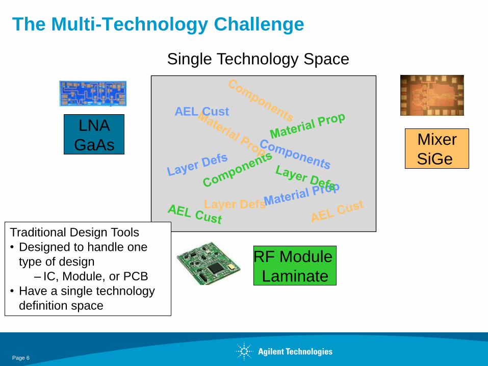
The Multi-Technology Challenge
LNA
GaAs Mixer
SiGe
RF Module
Laminate
Layer Defs
AEL Cust
Single Technology Space
Traditional Design Tools
• Designed to handle one
type of design
– IC, Module, or PCB
• Have a single technology
definition space
Page 6
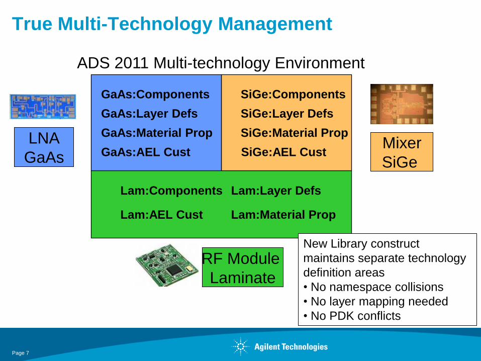
True Multi-Technology Management
LNA
GaAsMixer
SiGe
RF Module
Laminate
Lam:Components
Lam:Material Prop
Lam:Layer Defs
Lam:AEL Cust
SiGe:Components
SiGe:Material Prop
SiGe:Layer Defs
SiGe:AEL Cust
GaAs:Components
GaAs:Material Prop
GaAs:Layer Defs
GaAs:AEL Cust
ADS 2011 Multi-technology Environment
New Library construct
maintains separate technology
definition areas
• No namespace collisions
• No layer mapping needed
• No PDK conflicts
Page 7

Multi-Technology Design & Library Management
Page 8

Multi-Technology Simulation and Modeling
• Simulate critical circuits across multiple substrates
• Design closer to the margins
• Detect and solve issues before manufacturing
Page 9
Module
Laminate
Mixer
SiGe
LNA
GaAs

Native Physical Multi-Substrate Support
• Easily add one or more pre-defined
substrates
– IC in a package, IC in a module,
module on a board, etc.
• Unlimited levels of technology stacking
– i.e. IC on a module on a PCB
• Supports flip chips, wire bonding, and
backside mounting
• No modification of layers required
• Directly modify any of the designs
– No flattening required
• Works with all the ADS tools
– Layout, 3D Visualization, Momentum
and FEM, etc.
Easy to combine multiple substrates
Page 10
New graphical substrate editor

Page 11
ADS Integrated 3D EM FlowMomentum & FEM in ADS, 3D EM Components & EMPro/FDTD link
EMPro PlatformADS Platform
FDTD SimulatorFEM SimulatorMomentum Simulator
Parameterized
3D EM
Components
Layout
CAD Data

Multi-Technology EM SimulationCapabilities & Vision
• Discover coupling effects prior to
fabrication
• More effectively optimize design elements
for final packaging
• More easily make design trade-offs
• Help diagnose and solve performance
problems
Page 12
+ =
3D view FEMMomentum
+
Package IC IC
Multi-technology
EM Simulation
Improved RF Circuit Design and Simulation
Page 13

Views
Easily Manage Models & Design Representations
• Cells represent a single design
object
• Cell Views provide multiple
representations of that design
object
– Different schematic variants,
behavioral, measured, layout,
EM data views, etc.
– User defined
• Simplifies schematics
• Easily select simulation model
• Explore design variants
Cell name
Views
Page 14

Dynamic Simulation Model Selection
Design, by its nature, is evolutionary. Selecting model type and accuracy is key to this. This
makes it simple and virtually instantaneous.
• Easily select the model to use for
simulation
– Tradeoff speed vs. accuracy
• Works on one or more selected
components
• Current active model is shown on the
schematic
• Easily create a model priority list to
work on entire design hierarchy
Page 15

Control Model Selection Through Design Hierarchy
• User defined model priority policies
• Activate policy to specify which models
will be preferred
• Option to individually override
• Easy way to control model selection
for complex designs
– i.e. trade-off between speed and
accuracy
Page 16
Example “fast” policy
Example “accurate” policy
Selecting which policy to use

Major Improvements to Load PullFrom load pull to design in a few clicks
• New load pull data controller
– Handles Maury load pull data
• Direct, instant loading of load pull data
– Handles multiple files
– Easier review of data
• Immediately simulate matching network
– Easier design optimization, including
improved discrete optimization
– Automatic interpolation of scattered
measurement data
• Automatically display performance
parameters
Fast, Easy, Intuitive
Page 17

Data Display Improvements
• Improved Smith Chart graphics
– Better display of chart values
– Better overall look and data granularity
• Set color for a group of traces
– Easier interpretation of sweeps
• Improved Data Display Template Browser
– Real time quick search
– Direct editing of template properties
– Save As and Delete from the Browser
Page 18

Improved Accuracy for Conductor ModelsNew Multi-level Hemispherical Model
Available in Momentum and Circuit Simulation
Closer correlation to measured data Hammerstad
The original hemispherical model
Hemispherical
NEW Multi-level
2 4 6 8 10 12 14 16 180 20
-5
-4
-3
-2
-1
-6
0
freq, GHz
dB
(meas_2000m
il_ro
4350b..
S(2
,1))
dB
(yunhui_
bb4_hfc
orr
0..
S(2
,1))
dB
(S(2
,1))
dB
(yunhui_
bb4_hfc
orr
1_9..
S(2
,1))
SEM photograph of rough copper at
5000x magnification at a 30 degree angle.
Courtesy of Steven Hall et al. 2007
Measured Data
Agilent 5500
Atomic Force Microscope
• More accurately reflects conductor surface
• Can use AFM measurements to set params
Page 19

Other 2011 Improvements – Circuit Simulation
• Linear Simulation Speedup - up to 10X
– For fully-linear circuits with swept, tuned, or optimized simulations
• Improved Transmission line models (including multi-layer library)
– More accurate broad-band skin effect calculation
– New, advanced method of calculating surface roughness loss
– More accurate calculation of Power/Ground Plane loss
• Output simulator results in Matlab format
– New controller makes it possible to filter the output
• New models supported
– NXP SiMKit 3.4, PSP 102.3.4 and 103.1.1, Mextram 504.8, BSIMSOI 4.3.0, BSIM 4.6.5,
HiSIM_HV 1.2.0, MOSVAR 1.1, R3, PSPICE diode
• Support for Verilog A now included as part of ADS Core for use with all
simulators
Page 20

Making EM Simulation
Part of Everyone’s Design Flow
Page 21

New Graphical Layer Definition
• Graphical, unified entry of layer and stackup data
– Defines layers and properties for Layout, Momentum, and FEM
• Easy drag and drop operations
– Easily select and modify properties
• Simpler, faster, and less error prone
Page 22

New Streamlined EM SetupMaking EM Work for Everyone
• Single dialog replaces 8 – Easily navigate & review the setup options
• Same setup for Momentum, Momentum RF, & FEM
– Easy to try different solvers on the same design
• Setup is automatically saved and can be reused for other EM simulations
Previous EM Setup ADS 2011
Page 23

Reusing Saved EM Setup ConfigurationsMaking EM Work for Everyone
• Makes it possible for non-experts to create
accurate EM models
• Big productivity improvement for all users
• Easier to experiment with different setup
options
Foundry
PDK
EM
Expert
Packaged
With
ADS
Design
Engineer
Designer‟s
own setups
Saves Mouse Clicks (30 down to 3)
Use saved setups
on new work
Page 24
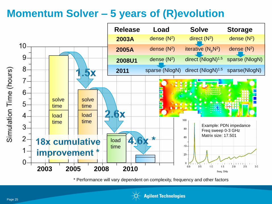
Example: PDN impedance
Freq sweep 0-3 GHz
Matrix size: 17.501
2005 2008 2010
solve
time
load
time
solve
time
load
time
load
time
2003
Release Load Solve Storage
2005A
2008U1
2011
dense (N2) direct (N3) dense (N2)
dense (N2) iterative (NpN2) dense (N2)
dense (N2) direct (NlogN)1.5 sparse (NlogN)
sparse (NlogN) direct (NlogN)1.5 sparse(NlogN)
2003A
Momentum Solver – 5 years of (R)evolution
Page 25
* Performance will vary dependent on complexity, frequency and other factors

Preprocessor Mesher (2nd generation ) Solver
New Momentum 2nd Generation Mesher
• Increased accuracy, robustness and performance
– Fast floating-point interval arithmetic
• Improved mesh quality
– Avoids slivers
– Improved handling of small and wide shapes
– New algorithm for edge mesh and overlap extraction
• Reduced mesh complexity
– New quadranglesrectangle
NEW
quadrilateral
triangle
Page 26
OLD
NEW

Improved Causal substrate model in Momentum
Dielectric Loss Model
• Uses the causal Svensson/Djordjevic model
• Same technology as in ADS circuit simulator
Substrate Material editor
Page 27

New Integrated EM Port Viewer/Editor
Features of new Port Editor
• Copy a value and paste to
multiple ports
• New filtering
– Quickly find ports by
attributes
– Filter on one or multiple
attributes
• Automatic port generation
• Automatic port re-
sequencing
Page 28
Auto
Multi-port Editor
Combined
Multi-port
Viewer & Editor
Single port Editor

Expanded Bondwire Support
• New, fast analysis of bondwires in Momentum
– Automatically modeled as part of Momentum
simulation
– Calculates self and mutual inductance
– FEM provides the most accurate analysis
• Bondwires work for both Momentum and FEM
– Easily create the bondwire in Layout
– Full parametric control of bondwire profile
• Jedec Bondwire – Follows the JEDEC
standard parameters
• Shape Bondwire – More flexible control of the
bondwire profile
• Bondwires now have edit handles
Page 29
Set parameters
Create and edit in 2D
Render in 3D

Performance w/ & w/o package
Accurately predict real performance
QFN DesignerPredict Packaged Performance in Minutes
Page 30
Quickly synthesize complex package,
combine with IC & PCB data
Configure QFN package

Layout Usability: Object Handles
• Directly work on objects – quick & efficient
• Objects with handles
– Arcs, Circles, Polylines, Polygons,
Rectangles, Text
– Transmission Lines, Paths, Wires,
Traces, Annotations, Wire Labels, Rulers,
Dimension Lines
• Infrastructure available for end user
customization
– Add handles to pdk components and
design kits
– Customizable behavior
Page 31

Layout Command Line & Toolbar
• Command line provides efficient keyboard entry for common functions
• User can add their own functions to the command line
• The toolbar provides single click operations for frequently used features
– Set vertex selection on/off, control pin-number display and align shapes
Page 32

Layout Command Line - Current Functions
Page 33

New Look: Redesigned IconsModern look, easier to understand, new icons: menu cmds
Schematic & Layout icons & toolbars
Command Line Editor & Toolbar
Page 34

Support for International Character Set
• Can create annotations / documentation with international characters
• Provided in schematic and data display
Page 35

Other 2011 Improvements
• Desktop LVS Viewer can now display Calibre errors
• Backside component support
• Allegro/ADS link (IFF for Allegro) now included in shipping product
• New entry mode for circles and rectangles
– Use CTRL key and first point will be the center of the shape
• New Array Reference (AREFs) objects to Layout
– Much more memory efficient way to create large arrays of objects
• Advanced Model Composer (AMC) models can now be created with FEM
• Layout connectivity engine is up to 40X faster than previous releases
• Layout layers can now have sub-layers (purposes)
– Can visually distinguish different objects drawn on a layer
Page 36
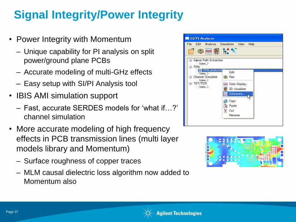
Signal Integrity/Power Integrity
• Power Integrity with Momentum
– Unique capability for PI analysis on split
power/ground plane PCBs
– Accurate modeling of multi-GHz effects
– Easy setup with SI/PI Analysis tool
• IBIS AMI simulation support
– Fast, accurate SERDES models for „what if…?‟
channel simulation
• More accurate modeling of high frequency
effects in PCB transmission lines (multi layer
models library and Momentum)
– Surface roughness of copper traces
– MLM causal dielectric loss algorithm now added to
Momentum also
Page 37

For More Information
Page 38
Agilent ADS 2011 Web page (new feature details)
www.agilent.com/find/eesof-ads2011
ADS 2011 on YouTube
www.youtube.com/user/AgilentEEsof
ADS 2011 Overview (Quick Start Video, Multi-technology Tutorials, …)
www.agilent.com/find/eesof-ads2011-overview

ADS 2011 Summary
• RF design has moved to complex ICs in multi-chip RF modules
• Today‟s design flows are not able to address multiple technology design
• The IC, laminate, package, and PCB need to be designed together
• Electro-magnetic interactions between substrates need to be modeled
• ADS 2011 is the only EDA software able to address these multi-
technology design challenges
• ADS 2011 is the only solution to the PI “split power/ground” problem.
Agilent EEsof EDA
“Innovative Solutions,
Breakthrough Results”
Page 39


![[Technical Paper] Thermal Performance of 3D IC Package](https://img.dokumen.tips/doc/110x75/61cfbd1528e41322d21d2625/technical-paper-thermal-performance-of-3d-ic-package-.jpg)