Embed Size (px)
Citation preview
Linköping Studies in Science and Technology
Dissertation No. 1305
The HiPIMS Process
Daniel Lundin
Plasma & Coatings Physics Division
Department of Physics, Chemistry and Biology
Linköping University, Sweden
2010

© Daniel Lundin 2010
ISBN: 978-91-7393-419-0
ISSN: 0345-7524
Printed by LiU-Tryck, Linköping, Sweden, 2010

I
Abstract
The work presented in this thesis involves experimental and theoretical studies related to a thin film deposition technique called high power impulse magnetron sputtering (HiPIMS), and more specifically the plasma properties and how they influence the coating. HiPIMS is an ionized physical vapor deposition technique based on conventional direct current magnetron sputtering (DCMS). The major difference between the two methods is that HiPIMS has the added advantage of providing substantial ionization of the sputtered material, and thus presents many new opportunities for the coating industry. Understanding the dynamics of the charged species and their effect on thin film growth in the HiPIMS process is therefore essential for producing high-quality coatings. In the first part of the thesis a new type of anomalous electron transport was found. Investigations of the transport resulted in the discovery that this phenomenon could quantitatively be described as being related and mediated by highly nonlinear waves, likely due to the modified two-stream instability, resulting in electric field oscillations in the MHz-range (the lower hybrid frequency). Measurements in the plasma confirmed these oscillations as well as trends predicted by the theory of these types of waves. Using electric probes, the degree of anomalous transport in the plasma could also be determined by measuring the current density ratio between the azimuthal current density (of which the Hall current density is one contribution) and the discharge current density, / DJ Jϕ . The results were verified in another series of measurements using Rogowski probes to directly gain insight into the internal currents in the HiPIMS discharge. The results provided important insights into understanding the mechanism behind the anomalous transport. It was furthermore demonstrated that the current ratio / DJ Jϕ is inversely proportional to the transverse resistivity, η⊥ , which governs how well momentum in the direction of the current is transferred from the electrons to the ions in the plasma. By looking at the forces involved in the charged particle transport it was expected that the azimuthally rotating electrons would exert a volume force on the ions tangentially outwards from the circular race track region. The effect of having an anomalous transport would therefore be that the ions were transported across the magnetic field lines and to a larger extent deflected sideways, instead of solely moving from the target region towards a substrate placed in front of the target some distance away. From the experiments it was confirmed that a substantial fraction of sputtered material is transported radially away from the cathode and lost to the walls in HiPIMS as well as in DCMS, but more so for HiPIMS giving one possible explanation to why the

II
deposition rate is lower for HiPIMS compared to DCMS. Moreover, in a separate investigation on the energy flux it could be determined that the heating due to radial energy flux reached as much as 60 % of the axial energy flux, which is likely a result of the anomalous transport of charged species present in the HiPIMS discharge. Also, the recorded ion energy flux confirmed theoretical estimations on this type of transport regarding energy and direction. In order to gain a better understanding of the complete discharge regime, as well as providing a link between the HiPIMS and DCMS processes, the current and voltage characteristics were investigated for discharge pulses longer than 100 μs. The current behavior was found to be strongly correlated with the chamber gas pressure. Based on these experiments it was suggested that high-current transients commonly seen in the HiPIMS process cause a depletion of the working gas in the area in front of the target, and thereby a transition to a DCMS-like high voltage, lower current regime, which alters the deposition conditions. In the second part of the thesis, using the results and ideas from the fundamental plasma investigations, it was possible to successfully implement different coating improvements. First, the concept of sideways deposition of thin films was examined in a dual-magnetron system providing a solution for coating complex shaped surfaces. Here, the two magnetrons were facing each other having opposing magnetic fields forcing electrons, and thereby also ionized material to be transported radially towards the substrate. In this way deposition inside tubular substrates can be made in a beneficial way. Last, the densification process of thin films using HiPIMS was investigated for eight different materials (Al, Ti, Cr, Cu, Zr, Ag, Ta, and Pt). Through careful characterization of the thin film properties it was determined that the HiPIMS coatings were approximately 5-15 % denser compared to the DCMS coatings. This could be attributed to the increased ion bombardment seen in the HiPIMS process, where the momentum transfer between the growing film and the incoming ions is very efficient due to the equal mass of the atoms constituting the film and the bombarding species, leading to a less pronounced columnar microstructure. The deposition conditions were also examined using a global plasma model, which was in good agreement with the experimental results.

III
Populärvetenskaplig sammanfattning
Denna avhandling beskriver experimentella och teoretiska studier av en beläggningsteknik för tunna filmer kallad ”High power impulse magnetron sputtering” (HiPIMS), vilket kan översättas med hög-effektspulsad magnetronsputtering. Tunna filmer är skikt av material med en tjocklek i storleksordningen ett fåtal atomlager till några mikrometer. Anledningen till att vi intresserar oss för denna typ av ytbeläggningar är främst möjligheten att kombinera egenskaper hos de tunna filmerna med övriga egenskaper från det underliggande materialet, ofta kallat substrat, för att därigenom erhålla förbättrade kemiska, mekaniska eller elektriska egenskaper. Därutöver kan helt nya fenomen uppstå när vi skalar ner tjockleken, vilket tillämpas inom elektronikindustrin och bidragit till populariteten kring så kallade nanomaterial. I dag hittar vi tunna filmer överallt i vår vardag, från antireflexbehandlade glasögon, aluminiumbeläggningen inuti chipspåsar, friktionsdämpande och nötningsbeständiga skikt i motorer till alla möjliga slags komponenter inuti datorer och mobiltelefoner. Själva beläggningstekniken HiPIMS bygger på en plasmabaserad metod där man skapar ytskikt under vakuumförhållanden. Genom att pumpa ut nästan all luft ur en vakuumkammare och därefter tillsätta små mängder av en gas, oftast argon, så kan man med hjälp av en pulsad elektrisk urladdning mellan två elektroder tända ett plasma, det vill säga jonisera den gas som finns där. Materialet som man vill använda i beläggningen (target) är placerat på en av elektroderna och är spänningssatt till minus flera hundratals volt under själva pulsen. Denna elektrod kallas även magnetron, då den dessutom består av ett magnetpaket som koncentrerar plasmat bättre till regionen ovanför target. Det innebär att de positiva jonerna i plasmat attraheras mot den negativa elektroden och bombarderar på så vis beläggningsmaterialet och stöter ut atomer, vilket kallas sputtering. De lösgjorda atomerna kan därefter färdas ut i vakuumkammaren och belägga substratet. Till skillnad från konventionell sputtering så genererar HiPIMS-processen ett cirka tusen gånger tätare plasma, vilket leder till att de sputtrade atomerna med stor sannolikhet kommer att kollidera med en elektron då de transporteras genom plasmat. Därmed genereras ett joniserat flöde av beläggningsmaterial (laddade partiklar), vilket i motsats till neutrala atomer kan styras med elektriska och magnetiska fält. Således har vi erhållit en ny möjlighet till att styra beläggningen och därigenom förbättra kvalitén på de tunna filmerna, vilket av naturliga skäl är av stort intresse för industrin.
IV
Fokus för denna avhandling har legat på att studera och karakterisera själva transporten av partiklar i HiPIMS-urladdningen med avseende på hastighet/energi och riktning för att därefter se hur förhållandena i plasmat påverkar filmtillväxten. I avhandlingen diskuteras en ny typ av anomal transport av elektroner, vilka färdas i vinkelrät riktning mot magnetronens magnetfält. Denna transport kan inte förklaras med klassiska kollisionsbaserade processer. Istället har vi funnit att det är en instabilitet som uppstår i plasmat, där en hastighetsskillnad mellan joner och elektroner leder till att oscillationer genereras och elektroner kan därigenom lättare transporteras tvärs magnetfältslinjer. En konsekvens av den anomala transporten är en kraft på jonerna, som innebär att de knuffas ut i en riktning parallell med magnetronytan och förloras till väggarna på vakuumkammaren, istället för att följa en rak kurs från target till substrat. Genom att utnyttja detta fenomen har vi visat att man kan belägga filmer av mycket god kvalitet och vidhäftning på komplexa substrat (icke-plana objekt) såsom insidan på rör. Dessutom har gasdynamiken under HiPIMS-processen studerats för att klargöra vad som händer under förloppet av en högeffektspuls samt perioden efter pulsen. Härigenom står det klart att pulsförloppet är starkt beroende av mängden tillgänglig gas, samt att det under urladdningen sker en stark uppvärmning av gasen vilket får den att expandera och därigenom förtunnas i området ovanför magnetronen. Ett viktigt resultat av detta är att gasförtunning leder till minskat jonbombardemanget på target och därmed minskad beläggningshastighet. Det finns således stora möjligheter att optimera pulskaraktäristiken i HiPIMS-urladdningen för att erhålla en bättre process. Slutligen visar vi också i praktiska experiment och genom datorsimulering att konsekvensen av ett joniserat flöde av beläggningsmaterial leder till tätare filmer av högre densitet jämfört med konventionell sputtering. Denna upptäckt är av stort intresse då man belägger så kallade diffusionsbarriärer och kan vara av stort värde för solcells- och bränslecellsindustrin. Vidare visas också att detta flöde inte nämnvärt hettar upp själva substratet, vilket möjliggör högkvalitativa tunnfilmer på temperaturkänsliga material såsom olika plaster.

V
Preface
The work presented in this doctorate thesis is a result of my PhD studies conducted since May 2006 in the Plasma & Coatings Physics Division at Linköping University. The goal of my doctorate project is to gain insight into the physics of HiPIMS plasmas as well as thin film growth using HiPIMS. The research is financially supported by the Swedish Research Council (VR), the Swedish Foundation for Strategic Research (SSF) and by the European Commission within the 6th framework (integrated project: InnovaTiAl). The results are presented in seven appended papers, which are preceded by an introduction giving an overview of the research field and describing the methods used in the research. The introductory chapters are to a large extent based and expanded on my previously published licentiate thesis1.
Linköping, April 2010
1 D. Lundin, Plasma properties in high power impulse magnetron sputtering, Linköping University, Linköping, Sweden (2008)

VI

VII
Publications included in the thesis
Fundamentals of HiPIMS plasma 1. “Anomalous transport in high power impulse magnetron sputtering”
D. Lundin, U. Helmersson, S. Kirkpatrick, S. Rohde, and N. Brenning Plasma Sources Sci. Technol. 17, 025007 (2008) Selected for inclusion in the IOP Select collection as well as Highlights of 2008 in Plasma Sources Science and Technology
2. “Cross-field ion transport during high power impulse magnetron sputtering”
D. Lundin, P. Larsson, E. Wallin, M. Lattemann, N. Brenning, and U. Helmersson Plasma Sources Sci. Technol. 17, 035021 (2008)
3. “Transition between the discharge regimes of high power impulse magnetron
sputtering and conventional direct current magnetron sputtering” D. Lundin, N. Brenning, D. Jädernäs, P. Larsson, E. Wallin, M. Lattemann, M.A. Raadu, and U. Helmersson
Plasma Sources Sci. Technol. 18, 045008 (2009) 4. “Thermal flux measurements in high power impulse magnetron sputtering” D. Lundin, M. Stahl, H. Kersten, and U. Helmersson J. Phys. D 42, 185202 (2009) 5. “Internal current measurements in high power impulse magnetron
sputtering” D. Lundin, S. Al Sahab, N. Brenning, C. Huo, and U. Helmersson In final preparation Fundamentals of HiPIMS growth 6. “Dual-magnetron open field sputtering system for sideways deposition of thin
films” A. Aijaz, D. Lundin, P. Larsson, and U. Helmersson Surf. Coat. Technol. 204, 2165 (2010) 7. “On the film density using high power impulse magnetron sputtering”
M. Samuelsson, D. Lundin, J. Jensen, M.A. Raadu, J.T. Gudmundsson, and U. Helmersson
Submitted for publication

VIII
My contribution to the included publications Paper 1 I was involved in the planning, performed the characterization and analysis, and wrote a major part of the paper. Paper 2 I was responsible for the planning, performed a large part of the characterization and analysis, and wrote the paper. Paper 3 I was involved in the planning, took part in the characterization and analysis, and wrote a major part of the paper. Paper 4 I was responsible for the planning, contributed to the characterization and analysis, and wrote the paper. Paper 5 I was responsible for the planning, performed a large part of the characterization and analysis, and wrote a major part of the paper. Paper 6 I contributed extensively to the planning, supervised the plasma characterization, film deposition and analysis, and was involved in writing the paper. Paper 7 I contributed to the planning, took part in the film deposition and film characterization as well as the analysis, performed the plasma modeling and wrote the paper.

IX
Related publications not included in the
thesis
1. “A bulk plasma model for DC and HIPIMS magnetrons” N. Brenning, I. Axnäs, M.A. Raadu, D. Lundin, and U. Helmersson Plasma Sources Sci. Technol. 17, 045009 (2008) 2. “On the electron energy in the high power impulse magnetron sputtering discharge” J.T. Gudmundsson, P. Sigurjonsson, P. Larsson, D. Lundin, and U. Helmersson J. Appl. Phys. 105, 123302 (2009) 3. “Faster-than-Bohm cross-B electron transport in strongly pulsed plasmas” N. Brenning, R. Merlino, D. Lundin, M.A. Raadu, and U. Helmersson Phys. Rev. Lett. 103, 225003 (2009)

X

XI
Acknowledgements
The investigations presented in this thesis are a result of a fruitful team work and I owe my deepest gratitude towards my co-workers for their great efforts and commitment. I would in particular like to acknowledge my two supervisors: Ulf Helmersson, for always asking difficult questions, making me progress, and most of all for believing in me and giving me the freedom to explore the world of plasma and thin films. Nils Brenning, for making me see the bigger picture. Your creativity and enthusiasm have guided me throughout my graduate studies. I would also like to thank my colleagues and friends in the Plasma & Coatings Physics division together with the Thinfilm Physics and Nanostructured Materials divisions, and here mention a few names: Petter Larsson, for being my co-pilot during most of the experiments. You steered me clear of failure on numerous occasions and helped me understand things that I was unable to see. Special thanks are also due to Mattias Samuelsson, Asim Aijaz and my former colleagues Daniel Jädernäs and Erik Wallin for joining me on these adventures. During my PhD studies I have had the honor to work with several great researchers around the world, whose help is invaluable to me:
o Catalin Vitelaru, Tiberiu Minea, Caroline Boisse-Laporte, Jean Bretagne and several others at Université Paris-Sud, France
o Jón Tómas Guðmundsson and Páll Sigurjónsson at the University of Iceland, Iceland
o Ingvar Axnäs, Michael Raadu and Jan Wistedt at the Royal Institute of Technology, Sweden
o Holger Kersten and Marc Stahl at the University of Kiel, Germany o Martina Lattemann at TU Darmstadt and Forschungszentrum Karlsruhe,
Germany o Jones Alami at Sulzer Metaplas, Germany o Johan Böhlmark at Sandvik, Sweden
I am indeed fortunate to have been among so many talented people. Last but not the least, I am very grateful towards my family and friends, the ones who are still around and the ones who departed, for all the support and love you have given me throughout all these years.

XII

XIII
Contents
ABSTRACT ......................................................................................................I
POPULÄRVETENSKAPLIG SAMMANFATTNING .......................................III
PREFACE....................................................................................................... V
PUBLICATIONS INCLUDED IN THE THESIS............................................. VII
RELATED PUBLICATIONS NOT INCLUDED IN THE THESIS.................... IX
ACKNOWLEDGEMENTS ............................................................................. XI
CONTENTS ................................................................................................. XIII
VARIABLES AND CONSTANTS ............................................................... XVII
1 INTRODUCTION ......................................................................................1
1.1 Thin film growth ......................................................................................................................1
1.2 Thin film deposition .................................................................................................................1
1.3 Purpose and outline..................................................................................................................3
2 PLASMA FOR MATERIAL PROCESSING..............................................5
2.1 Background...............................................................................................................................5
2.2 Plasma for thin film deposition ...............................................................................................5
2.3 Plasma fundamentals ...............................................................................................................8
2.4 Sputtering ...............................................................................................................................11
3 PLASMA DYNAMICS ............................................................................15
3.1 Particle motion .......................................................................................................................15
XIV
3.2 Plasma oscillations .................................................................................................................17
3.3 Plasma transport ....................................................................................................................18
3.4 Diffusion and resistivity .........................................................................................................20
3.5 Plasma instabilities.................................................................................................................22
3.6 Anomalous transport .............................................................................................................25
4 PLASMA ANALYSIS .............................................................................29
4.1 Background.............................................................................................................................29
4.2 Electrostatic probes................................................................................................................29
4.3 Magnetic probes .....................................................................................................................31
4.4 Langmuir probes....................................................................................................................32
4.5 Thermal probes ......................................................................................................................35
4.6 Mass spectrometry .................................................................................................................37
5 PLASMA MODELING ............................................................................39
5.1 Background.............................................................................................................................39
5.2 Global models .........................................................................................................................40
6 MAGNETRON SPUTTERING ................................................................43
6.1 Background.............................................................................................................................43
6.2 Ionized PVD............................................................................................................................45
7 HIPIMS ...................................................................................................47
7.1 Background.............................................................................................................................47
7.2 Fundamentals of HiPIMS......................................................................................................47
7.3 Challenges facing HiPIMS.....................................................................................................50
8 THIN FILM CHARACTERIZATION ........................................................53
8.1 Background.............................................................................................................................53
8.2 Scanning electron microscopy...............................................................................................53
8.3 Ion beam analysis ...................................................................................................................55

XV
9 SUMMARY OF RESULTS......................................................................59
9.1 Paper 1 - Anomalous electron transport in high power impulse magnetron sputtering ................................................................................................................................59
9.2 Paper 2 - Cross-field ion transport during high power impulse magnetron sputtering ................................................................................................................................60
9.3 Paper 3 - Transition between the discharge regimes of high power impulse magnetron sputtering and conventional direct current magnetron sputtering ................60
9.4 Paper 4 - Energy flux measurements in high power impulse magnetron sputtering ................................................................................................................................61
9.5 Paper 5 - Internal current measurements in high power impulse magnetron sputtering ................................................................................................................................62
9.6 Paper 6 - Dual-magnetron open field sputtering system for sideways deposition of thin films .............................................................................................................................62
9.7 Paper 7 - On the film density using high power impulse magnetron sputtering ..............63
10 ONGOING AND FUTURE RESEARCH .................................................65
11 REFERENCES .......................................................................................67
PAPER 1-7 ....................................................................................................73

XVI

XVII
Variables and constants
B magnetic field vector c speed of light C heat capacity D diffusion coefficient D dielectric field vector ε0 permittivity of free space e elementary (electron) charge E electric field vector Φ flux F force vector η resistivity I current J current density vector k Boltzmann’s constant; wave number or wave vector (k) λD Debye length μ0 permeability of free space m electron mass M ion mass n density ω angular frequency p pressure P power ρ charge density rL Larmor (gyro) radius Rc radius of magnetic field line curvature σ cross sectional area; conductivity τ collision time T temperature u fluid velocity v particle velocity V electric potential

XVIII

1
1 Introduction
1.1 Thin film growth Thin films are layers of material with a thickness ranging from a few atomic layers (~nm) to a few micrometers, and can today be found just about everywhere in our society; from anti-reflective coatings on eyeglasses to computer chips. The advantage is the combination of the surface properties of the thin film with the bulk properties of the underlying material, leading to enhanced chemical, mechanical or electrical properties to name a few. Furthermore, new physical properties sometimes arise for objects in the nanoscale size range, which is for example used in the electronic industry. The history of making thin films dates back to the metal ages, and particularly to the ancient craft of gold beating. The Egyptians were the first to practice this art about 4000 years ago [1], which a multitude of different jewelry bear witness about. Famous examples are the decorative gold leafs from ancient Luxor with a thickness of about 0.3 micrometers. As a reference a normal sheet of paper is about 100 micrometers. However, thin films used in other cases as for mere decorative purposes were produced much later. In the early 1800s, electroplating, the first widespread thin film deposition technique, was invented by the Italian chemist Luigi V. Brugnatelli [2]. The resulting thin films were not of great quality. Instead it was in 1852, when W.R. Grove first studied what became known as sputtering [3] (a way of depositing thin films, which will be discussed in more detail in section 2.4), that modern thin film science began. Grove used a tip of wire as the coating source and sputtered a deposit onto a highly polished silver surface held close to the wire at a pressure of about 0.5 Torr. In 1878 A.W. Wright of Yale University published a paper in the American Journal of Science and Arts on the use of an “electrical deposition apparatus” that he used to create mirrors [4]. At about the same time the famous T. Edison filed a patent application for vacuum coating equipment to deposit coatings on wax cylinder phonographs [5, p. 11]. Since it could not be proven certain that Wright had used sputtering to produce these thin film mirrors, it meant that Edison won in court on being the inventor to thin film deposition through sputtering. Edison could therefore be said to be the first person to make commercial use of sputtering.
1.2 Thin film deposition There are numerous ways of producing thin films, such as electroplating, evaporation, sputter deposition, chemical vapor deposition and combinations of these methods. Here, only the most commonly used methods will be discussed followed by a brief description of a recently developed technique called high power impulse magnetron sputtering (HiPIMS), which has been the main technique used in this thesis. The

2
interested reader is referred to references 6 and 7 for more information on thin film deposition. Electroplating is very common within industry [8] and is one of the most simple and cost effective processes for depositing metal coatings. Here, the object to be coated is lowered into a solution (for example an acid), into which a metal is dissolved. By applying a negative charge to the object, positive metal ions are attracted, and a coating forms on the surface. Unfortunately high-quality, dense, defect-free films are hard to achieve using this method, which also produces considerable amounts of hazardous waste. Two other widespread methods, known to produce thin films of greater quality are chemical vapor deposition (CVD) [6, chapter 6] and physical vapor deposition (PVD) [6, chapter 5]. For CVD, volatile gases (precursors) are let into a deposition chamber. By adding heat, the gas will start to react and form new reactive species. The initial gas as well as the new products will diffuse and form a coating on any surface present in the chamber [6, p. 279]. The technique is widespread within industry, since it provides a high productivity and has the advantage of generating homogenous coatings on complex-shaped surfaces. Another reason for using CVD is the ability to deposit a great variety of coatings, from metals to organic compounds with high control of the coating composition [6, p. 278]. One major drawback in CVD is that very high temperatures are needed to make the different constituents react in the gas phase on a surface [6, p. 286]. This means that several applications are excluded due to the risk of melting and/or damaging the object to be coated (in thin film deposition we usually call this a substrate). For example, different thermal expansion coefficients between the coating and the substrate make CVD less suitable for coatings on steel, plastics and electrical components. In some cases this problem can be solved by using a plasma2 instead of heating, to activate the process (so called plasma-enhanced CVD) [9]. PVD is a general term describing how films are deposited by the condensation of a vaporized form of a material onto various surfaces. The vapor of the thin film material is created by physical means from a solid deposition source. One such PVD method is sputter deposition [6, chapter 5]. Here, the deposition source is often called a target and atoms from it are evaporated by physical bombardment of particles from for example a plasma3 inside the deposition system. These atoms are then transported through the deposition chamber and condensate at the substrate, forming a film. The process is in general based on a diode configuration with facing electrodes constituting the anode and the cathode, where the plasma is located in between. In such an arrangement the target plays the role of the cathode. The most common PVD methods are arc evaporation and magnetron sputtering (see for example reference 10 for more details). Strictly speaking, sputtering is not the mechanism used in arc evaporation. Instead an extreme high-current discharge is used to melt the target material in a small spot and eject it out into the chamber. Coatings made by arc evaporation have in general good adhesion, but sometimes a rough film 2 A plasma is defined as a collection of freely moving charged particles that is in average electrically neutral. We will learn more about plasmas in the next chapter. 3 In sputter deposition, the plasma is created by letting in a gas followed by applying an electrical discharge of hundreds of volts.

3
surface due to the presence of macroparticles from the process. In magnetron sputtering an external magnetic field is used to better confine the plasma close to the sputtering region, which we will look more into in chapter 6. The advantage of this configuration is higher deposition rates compared to simple DC sputtering without magnetic confinement as well as reduced background gas pressure [6, p. 222-223], which results in coatings of good quality with very low levels of impurities [11]. In 1999 a new PVD technique based on magnetron sputtering, called HiPIMS was developed by Kouznetsov [12], building on previous works by Mozgrin et al. [13] Bugaev et al. [14] and Fetisov et al. [15]. It used high-power pulses to ionize more of the sputtered material, which led to additional improvement of the thin film quality and will be further discussed in chapter 7. Until his death in 2008, Kouznetsov filed several HiPIMS patents (see for example reference 16 ), which he put into his company Chemfilt AB (later called Chemfilt Ionsputtering AB). There are many advantages inherent to the HiPIMS process. It is very easy to set up if a conventional magnetron sputtering system is present. In principle, all you need to change is the power supply. Furthermore, with a large fraction of ionized sputtered material, the resulting coatings have been found to be denser and one can also control the deposition flux to a much greater extent using for example an external bias (see section 7.2 and references therein). In addition, already in the early days of HiPIMS it was discovered that that the transport of charged particles in this type of plasma is more efficient than can be explained by standard theory [17, 18]. It is by obvious reasons very interesting to further investigate this promising technique and in particular the dynamics of the plasma as well as understand what underlying mechanisms are responsible for the change in thin film properties.
1.3 Purpose and outline The purpose of this work has been to expand on existing HiPIMS studies and models of plasmas to include recent findings in the field of plasma transport. Both experiments and theory have been worked out in order to achieve a better understanding of the HiPIMS plasma and possible consequences of the mechanisms operating in this type of discharge. Furthermore, investigations on the lower deposition rate for HiPIMS compared to conventional sputtering have been carried out. One of the main motivations for this work, besides the fundamental knowledge gained, has been to make HiPIMS an industrially attractive thin film deposition technique, which has meant including studies related to thin film deposition using HiPIMS as well as characterization of the resulting films. The outline of the introductory chapters preceding the papers is as follows. First a general overview of plasma physics used in thin film growth, and sputtering in particular, is given. This is followed by a chapter on the plasma dynamics in order to understand the principles behind the transport of charged particles. After this, the basic principles of the plasma analysis techniques used are presented as well as a chapter on plasma modeling. Magnetron sputtering and particularly HiPIMS are then developed in the chapters that follow. In addition, a chapter on the thin film characterization techniques employed in this work is also included. The thesis is concluded with a summary of the results and a short outlook, which hopefully will inspire future work in this field of research.

4

5
2 Plasma for material processing
2.1 Background Historically the term ‘plasma’ was introduced by Irving Langmuir in 1928 [19] when he investigated oscillations in an ionized gas. He used the word to describe a region containing a balanced number of charges of ions and electrons. Today we define a plasma as a collection of freely moving charged particles that is in average electrically neutral [20, p. 6], and we often refer to it as the “Fourth State of Matter” because of its unique physical properties, distinct from solids, liquids and gases. Examples of plasmas include the sun (and other stars) and the aurora borealis (northern light), making up about 99% of our visible universe4 [21, p. 1]! We can also observe a plasma in for example fluorescent light bulbs, neon signs and lightning. A plasma is sometimes erroneously called an extremely hot gas, but by heating up a gas it is possible to create a plasma. At a sufficiently high temperature the gas molecules will decompose to form freely moving gas atoms. If the temperature is further increased these gas atoms will release some of their electrons resulting in free, randomly moving electrons and ions. A plasma has been generated if enough gas atoms are ionized making the collective motion controlled by electromagnetic forces. Even in a weakly ionized plasma5 the dynamics of the system is governed by effects caused by a small number of strongly interacting ions and electrons compared to the large number of weakly interacting neutrals.
2.2 Plasma for thin film deposition As was briefly described in the introductory chapter, the common way of generating a plasma for material processing by magnetron sputtering is to use two metal electrodes: a cathode and an anode (usually the grounded chamber walls) enclosed in an evacuated vacuum chamber. In order to generate the plasma a source of power is needed, such as a direct current (DC) power supply. A simple sketch describing this typical setup is seen in Figure 1.
4 The discussion on dark matter is here disregarded. 5 Only a small fraction of the atoms are ionized.

6
PS
M
AC/DC
TMP
FVP
gas
Figure 1. Schematic drawing of a simple sputter deposition system showing a deposition chamber connected to a power supply (PS). The deposition chamber consists of a top-mounted magnetron and target (M). A turbo molecular pump (TMP) and a fore vacuum pump (FVP) are also connected to the chamber. A substrate is placed in the center on a substrate table and is immersed in the plasma (sketched below the magnetron). Through a gas inlet (lower-right in the system) a working gas, such as argon, is let in. A working gas, such as argon (Ar) is introduced into the chamber. The gas serves as the medium where the electrical discharge is initiated and sustained. The pressure used is around 1 mTorr - 1 Torr (0.13 – 133 Pa). By applying a few hundred volts6 to the cathode there will be a visible glow between the cathode and the anode, and a plasma is being maintained from this glow discharge [ 22 ]. The mechanism of transferring the working gas to a plasma can be seen as the analog of dielectric breakdown in an insulating solid, where the dielectrics will start conducting current at a critical voltage. In the case of the gas it starts with a free electron, caused by e.g. background radiation or thermal energy, being accelerated towards the anode by an electric field, created by the voltage difference applied between the electrodes. The accelerated electron will gain energy and eventually collide with neutral gas atoms and ionize them. The following reaction will take place:
e- + Ar → 2e- + Ar+.
The resulting two electrons can now bombard two other neutrals, while the Ar ion will be accelerated and collide with the cathode releasing, among other particles, electrons (often called secondary electrons). This regime is called the Townsend discharge [6, p. 149-150], and very little current is flowing due to the small amount of charge carriers (see Figure 2). The cascade of ionizing collisions will ultimately result in a large current causing the gas to break down, and eventually the discharge becomes self-sustaining, meaning that enough secondary electrons are generated to produce the required amount of ions to regenerate the same number of electrons. The gas begins to glow and there is a sharp voltage drop, and we are now in the normal glow regime [6, p. 150]. With increasing power the current density will eventually be rather evenly distributed over the entire cathode surface. If one increases the power even further the abnormal 6 This is valid for magnetron sputtering. Without the confining magnetic field several kV are required.
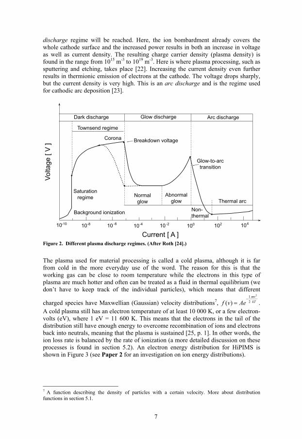
7
discharge regime will be reached. Here, the ion bombardment already covers the whole cathode surface and the increased power results in both an increase in voltage as well as current density. The resulting charge carrier density (plasma density) is found in the range from 1015 m-3 to 1019 m-3. Here is where plasma processing, such as sputtering and etching, takes place [22]. Increasing the current density even further results in thermionic emission of electrons at the cathode. The voltage drops sharply, but the current density is very high. This is an arc discharge and is the regime used for cathodic arc deposition [23].
Volta
ge [
V ]
Current [ A ]
Dark discharge Glow discharge Arc discharge
Townsend regime
Breakdown voltageCorona
Glow-to-arctransition
Thermal arcAbnormal
glowNormal
glow
Saturationregime
Background ionization Non-thermal
10 10 10 10 10 10 10 10-10 -8 -6 -4 -2 0 2 4
Figure 2. Different plasma discharge regimes. (After Roth [24].)
The plasma used for material processing is called a cold plasma, although it is far from cold in the more everyday use of the word. The reason for this is that the working gas can be close to room temperature while the electrons in this type of plasma are much hotter and often can be treated as a fluid in thermal equilibrium (we don’t have to keep track of the individual particles), which means that different
charged species have Maxwellian (Gaussian) velocity distributions7, 21
2( )mvkTf v Ae
−= .
A cold plasma still has an electron temperature of at least 10 000 K, or a few electron-volts (eV), where 1 eV = 11 600 K. This means that the electrons in the tail of the distribution still have enough energy to overcome recombination of ions and electrons back into neutrals, meaning that the plasma is sustained [25, p. 1]. In other words, the ion loss rate is balanced by the rate of ionization (a more detailed discussion on these processes is found in section 5.2). An electron energy distribution for HiPIMS is shown in Figure 3 (see Paper 2 for an investigation on ion energy distributions).
7 A function describing the density of particles with a certain velocity. More about distribution functions in section 5.1.

8
0 5 10 15 20 25 30 35 40 45−2
0
2
4
6
8
10
12
14
16x 10
17 The Electron Energy Distribution Function (EEDF)
Electron energy [ eV ] Figure 3. An electron energy distribution taken in a HiPIMS discharge 80 μs after pulse initiation. Here we see a large fraction of low-energy electrons as well as a small high-energy tail. Note that the signal is rather weak above 12 eV and the noise is here affecting the recorded value. (Courtesy of A. Aijaz.) A common misunderstanding is that a high temperature is connected to great heat transfer. The reason why the hot electrons do not melt the whole system is because there are so few of them inside the chamber, which means that the heat conduction is very low.
2.3 Plasma fundamentals Now we have come to a situation where a plasma is maintained in the vacuum chamber. Since plasmas can be considered as charged fluids, they will obey Maxwell’s equations, meaning that electromagnetic forces will govern the particle motion in a rather complex way8. Later on a more detailed study of the particle orbits will be presented. For the moment let us have a look at how the plasma interacts with the wall of the chamber by investigating one of Maxwell’s equations called the Poisson equation (or Gauss’ law), 0 ( )i ee n nε∇ ⋅ = ∇ ⋅ = −D E , (2.1) where ni and ne are the positive ion and electron densities respectively. The equation relates the electric field to the charge balance at a certain point. By using the fact that the electric field can be derived from a potential according to
8 As will be shown in the next chapter, the particle motion is described by Maxwell’s equations coupled with the Lorentz force equation. Another aspect of the plasma is the fluid character, meaning that fluid equations will come into play. This will not be discussed here.

9
V= −∇E (2.2) the following expression can be derived 2
0( / )( )i eV e n nε∇ = − − . (2.3) Equation (2.3) can be solved using the Boltzmann relation9 ( /
0eV T
en n e= with Te given in eV) [21, p. 9-10], the approximation 0in n≈ and the boundary conditions 0V =
when x →±∞ . In 1D this results in /0
DxV V e λ−= , where
1/2
0
0
eD
Tenελ
⎛ ⎞= ⎜ ⎟⎝ ⎠
(2.4)
is called the Debye length. It is the length scale on which charge densities can exist; on greater distances charge imbalances do not affect the plasma. In the case of processing plasmas λD usually amounts to at least a few tens of μm. This is indeed a very important finding, because it leads to the notion that in the bulk of the plasma there are more or less equal amounts of negative and positive particles (ni ≈ ne = n0) making the plasma quasineutral. Here n0 is the plasma density. The only place where the quasineutrality can be violated is in the sheath between the plasma and another boundary such as the chamber walls. In reality the thickness of the sheath is found to be about 5λD [25, p. 5]. In the sheath the ions outnumber the electrons, or ni > ne. The potential of the wall is negative relative to the plasma due to fact that the electrons move faster than the ions and therefore leave the plasma to a greater extent. This process goes on until a large enough potential difference between the plasma and the walls has been built up resulting in a negative, repelling sheath drop. Thus the plasma potential, Vp, is often positive (usually a couple of volts) relative the walls, see Figure 4. Furthermore, we have to keep in mind that these loss processes will not deplete the plasma of charge carriers as long as we uphold the large potential drop on the cathode, since electrons are continuously fed into the plasma through secondary electron emission and ionization processes in order to sustain the plasma (these balancing processes are discussed more in section 5.2). Also worth mentioning is that objects not connected to ground, introduced in the plasma will in general take on a slightly negative potential with respect to the plasma potential. This is known as the floating potential, Vf, and is also due to the higher mobility of the electrons. How this knowledge can be used in practice is discussed in section 4.4 on the Langmuir probe technique.
9 The Boltzmann relation gives the electron plasma density depending on the plasma potential and electron temperature, which is valid in the absence of high-frequency variations.

10
Anodesheath
AnodeCathode
0
Potential
Vp
Cathodesheath
Figure 4. Potential distribution from a DC discharge. Here the cathode is the negatively biased magnetron and the anode is the chamber walls. Vp is the plasma potential. The fall in potential is indicated for each sheath region. (Adapted from M. Ohring [6].) Regarding material processing, the discussion on sheaths become very important, since the ions naturally gain a directed velocity when coming close to and eventually strike the chamber wall or a substrate placed in the chamber [25, p. 9]. The reason for this is the imbalance ni > ne found in the sheath, which leads to the Bohm sheath criterion [20, p. 169], stating that ions will stream into any sheath with a velocity, us, at least as large as the ion acoustic velocity, cs:
1/2
es s
eTu cM
⎛ ⎞> =⎜ ⎟⎝ ⎠
(2.5)
The obvious question is then why the ions get a much larger, directed velocity compared to the thermal velocity one would expect them to have? The answer is that there is a small electric field in the presheath, between the plasma and the sheath, which accelerates ions to an energy of at least ½(kTe) [25, p. 9]. Thus, the plasma can exist with a material boundary (such as a chamber wall) only if there is an isolation consisting of a sheath and a presheath. As we previously discussed, there is a potential drop in the sheath repelling electrons and at the same time attracting ions to the boundary. At a non-conducting wall this potential drop adjusts itself automatically so that an almost equal flux of ions and electrons are leaving the bulk plasma and thereby preserving quasineutrality.
In magnetron10 processing plasmas it also becomes important to investigate high-voltage sheaths, since a high voltage is applied to the cathode in order to ignite the plasma. There are a few theories about the sheath evolution in this case, such as the matrix sheath model and the Child law sheath, both described by Lieberman and Lichtenberg [20, p. 175-178]. We will here focus on the widely used Child law sheath, which comes about assuming that the electron density can be neglected in a region close to the negative cathode. Without going through the derivations, the Poisson equation is solved with the assumption of a constant ion current density, which is found to be
10 For magnetrons see chapter 6.
11
1 2 3 2
00 0 2
4 29
VeJM s
ε ⎛ ⎞= ⎜ ⎟⎝ ⎠
, (2.6)
Where -V0 is the cathode potential and s is the sheath thickness. With the general expression for current density eJ en u= and setting su c= as derived above, it is possible to write the high-voltage sheath thickness as
3 4
0223 D
e
VsT
λ⎛ ⎞
= ⎜ ⎟⎝ ⎠
. (2.7)
For a typical magnetron plasma the Child law sheath can be around 100 Dλ or slightly less than 1 cm (around 1 mm in the HiPIMS case). According to the previous assumption that this region is devoid of electrons the gas will here not be excited and the sheath region therefore appears dark, which was already early on discovered in the experiments with gas discharges [21, p. 295].
2.4 Sputtering A phenomenon that is not part of the discharge dynamics, but important for the growth of thin films, is cathode sputtering, which is a process where material from the cathode is ejected by impinging positive gas ions from the plasma11. In more detail, the gas ions found in the discharge cross the sheath region while gaining energy, strike the cathode surface and physically remove (or sputter away) cathode atoms through momentum transfer [6, p. 174-180]. In 1852 W.R. Grove was the first to study what became known as “sputtering” although others had observed the effect while studying glow discharges [3]. Besides sputtering, incoming ions can also stick to the surface (adsorb), scatter, or get implanted in the first few atomic layers of the cathode. A few other events can also take place, such as surface heating 12 and alteration of the surface topography, making ion bombardment into something we can see as playing a round of “atomic pool” [6, p. 171 and p. 174]. What the outcome will be when an incoming ion breaks up the close-packed atoms in the cathode material is highly dependent on the material properties and ion energy [26]. It is therefore meaningful to introduce the concept of sputter yield, S(E), as number of sputtered atoms per incident particle [6, p. 174]. For the most commonly used materials (such as Cu, Ti and Cr) the sputter yield is in the range of 0.5 – 2, which for example can be seen by using the free software package SRIM [27], simulating ion-matter interactions based on numerous experimental results. It is in general good to have as high sputter yield as possible, since this means a higher deposition rate of sputtered material. The main events of sputtering have been identified based on a sputtering theory due to P. Sigmund [28]: a) Single knock-on (low energy), b) linear cascade, and c) spike (high energy). In principle one can summarize it as the higher the incoming ion energy, the 11 This is true in the case of thin film deposition using magnetrons, but other types of bombarding particles can be used. We can for example also have metals sputtering metals, which is discussed below in this section. Furthermore, in the sputtering event electrons are also ejected and they are usually called secondary electrons. 12 A substantial fraction of the kinetic energy of the ion is used for heating up the target.

12
greater the chance to affect several atoms in the bulk material resulting in more collisions and more sputtered atoms. This is true up to a certain energy (usually around 100 keV) [29], after which we often detect a drop in the sputtering yield due to less interaction between the incoming ion and the bulk atoms (reduction of the nuclear stopping power). Finally, after an atom has been sputtered it is available to interact with the plasma. Before moving on to studying the dynamics of the individual particles in the plasma, let us first get a general overview of the collective behavior of the sputtered particles as well as gas particles present in the bulk plasma. The below given description is based on a target material pathway model by Christie [30], which was later on improved by Vlcek et al. [31]. Also added to the picture is a discussion on the gas dynamics, which is taken from Paper III. Figure 5 shows a schematic view on the collective particle dynamics, where the roman numerals correspond to the different processes taking place (described below).
A
G M
lost lost
Target
Substrate
II
III
I
IV
V
VI
VII
VIII
IX
X
XI
XII
Figure 5. Schematic of the phenomenological model for ionized plasma magnetron discharges based on works by Christie [30], Vlcek et al. [31] and Lundin et al. [32]. The letters G and M respectively stand for gas and metal ions. Starting from the target side, where the sputtering takes place it is straightforward to realize that two types of ions can be accelerated over the high voltage sheath region

13
and impinge on the target surface, namely gas ions (I) and also metal ions (II) that have previously been sputtered and then ionized. These two types will sputter away different amounts of target material depending on their respective sputter yield (III). A factor that is affecting this rate is the applied voltage to the target, V0, in a way such that 0( ) ~S E V [33]. In general, the sputter yield also increases for heavier inert gases (argon has a higher sputter yield than helium), with a correction due to better momentum transfer for similar masses of the particles involved in the collision (for example, argon sputters more zirconium than what xenon does) [34]. As a rule of thumb the self-sputter yield (target ions sputtering the target) is lower than the argon sputter yield [35]. After the sputtering event the target material (metal) neutrals are transported out into the plasma. On their way to the substrate there is a probability of an ionizing event (IV) through for example a collision with an electron (for more details on this type of interactions see section 5.2). A fraction of those ions will be close enough to the cathode fall having a low enough kinetic energy as to be back-attracted to the target surface (V) and take part in the sputtering [30]. Controlling the potential profile in the cathode region will therefore greatly affect the number of metal ions incident on the target surface [36]. The rest of the ions will escape into the bulk plasma (VI), where they either will be lost to the walls or end up at the substrate position (VII). Regarding the sputtered neutrals that have not undergone an ionizing collision a few things can happen: They might later on be ionized in the bulk of the plasma (VIII) due to enhanced electron confinement (see section 6.1 on magnetrons), while being too far away to be affected by the negative potential drop, lost to the chamber walls, or arrive at the substrate to take part in the film growth (IX). During the transport there is also a likelihood that metal neutrals will collide with the neutral gas background (X). These collisions lead to heating of the gas followed by expansion (decrease in gas density in front of the target), in a process that is called gas rarefaction. It has extensively been investigated in magnetron discharges both experimentally and theoretically [37, 38, 39, 40, 41] during the last three decades. Up till now we have neglected that a few percent of the bombarding gas ions will not participate in sputtering, but merely be neutralized at the target surface and reflected back to the plasma (XI). These reflected sputtering gas atoms will have an inherently high energy, since they were first accelerated towards the cathode (as ions) by the high potential cathode fall and most of that energy was not transferred to the target atoms [42]. A fraction of the reflected gas neutrals will also collide with the neutral background (XII) and thereby enhancing the gas rarefaction, while others will quickly leave the bulk plasma region and be pumped away. The reduction of gas density would not be much of a problem if the refill process would be fast enough. Unfortunately this does not seem to be the case in all types of magnetron discharges, and it is believed to be particularly serious in HiPIMS [43], which is also further investigated in Paper III.

14

15
3 Plasma dynamics
3.1 Particle motion Due to the rather complex nature of a plasma, which in some sense can be described as an ordered system of particles and at the same time as a disordered fluid, it is not always straightforward to analyze. Still we can try to find a way to see what is happening inside the plasma, also called the plasma dynamics, by studying some simple cases of particle motion. As we have previously seen the plasma consists of a large number of charged particles and thus Maxwell’s equations describe the behavior of electric and magnetic fields affecting these species [20, p. 24].
t
∂∇× = −
∂BE (3.1)
0 2
1c t
μ ∂∇× = +
∂EB J (3.2)
0
ρε
∇⋅ =E (3.3)
0∇⋅ =B . (3.4) They contain very important information in the field of electromagnetism, which have helped us to understand a great part of the physics in today’s modern society: from radio and TV communication to various space phenomena. Here E is the electric field, B is the magnetic field, ρ is the charge density, and J is the current density. Equations (3.1) (Faraday’s law of induction) and (3.2) (Ampère’s circuital law) relate the spatial and temporal behavior of the electric and magnetic fields to each other. They can be combined to form a wave equation, telling us how electromagnetic waves propagate (more about waves in plasmas in section section 3.5 and Paper 1). Equation (3.3) (Gauss’ law) states that an electrical charge will give rise to a divergent electric field, and equation (3.4) (Gauss’ law for magnetism) tells us that there are no magnetic monopoles. This means that cutting a magnetic compass needle in two will not result in one piece attracted towards north and the other attracted towards south, but instead two smaller, ordinary compass needles. Another, often used equation is the continuity equation [21, p. 66],
( ) 0n nt
∂+∇ ⋅ =
∂u , (3.5)

16
which states that, in the absence of ionization and recombination, the particles in the plasma are conserved. u is the fluid velocity and n the density. The reason for mentioning it at this point is that it governs the overall behavior of all particles and we will learn more about treating the plasma as a fluid in chapter 5. Now we return to the matter of trying to describe the behavior of the plasma. Fortunately it is possible to look at single particle motion and thereby get a feeling for the plasma dynamics. The equation that describes the motion of a charged particle under the influence of electric and magnetic fields is called the Lorentz force equation [20, p. 27]: ( )q= + ×F E v B (3.6) Here F is the force acting on a particle of charge q and velocity v in the presence of an electric field E and a magnetic field B. This equation states that a positively charged particle will be accelerated along the direction of the electric field (in the opposite direction had it been a negatively charged particle), and it will move in circles around a guiding center in a plane perpendicular to the magnetic field [25, p. 22]. The resulting motion 13 (or drift velocity), ( ) 2
E B B= ×v E B , will be directed perpendicular to both E and B, as displayed in Figure 6.
+
.E
B
vE/B
Ion Electron
Figure 6. Single particle motion in combined electric and magnetic fields. B points out of the plane of the paper. (Adapted from F. F. Chen [21].) The drift is usually called Hall drift or E B drift, due to the fact that the drift velocity for both positively and negatively charged particles is E B ∝v E B . Furthermore, the radius of the gyrating motion is called the Larmor radius [21, p. 20] and is roughly about 1 mm for an electron and on the same scale as the vacuum chamber (tens of cm)
13 We are here only considering charge particle motion perpendicular to B.
17
for an ion for the type of plasma described in this thesis (more details on how to calculate the Larmor radius is found in section 4.4). This means that the electrons are well confined in the plasma due to the small gyration radius. The ions on the other hand, having a much larger gyration radius, can more or less freely cross the magnetic field lines and are therefore weakly confined. In PVD plasmas, the plasma dynamics consists of more than the E/B drift. Other important drift velocities (which are more thoroughly described in Paper 1) are: (1) the curved magnetic vacuum field gyro centre drift, ,e Ru , which for an isotropic Maxwellian distribution can be written as [21, p. 30]:
, 2 2
2 e ce R
c
kTe R B
×=
R Bu (3.7)
and (2) the pressure gradient (or diamagnetic drift) drift, ,e pu ∇ [21, p. 69]:
, 2e pe
pen B∇∇ ×
=Bu . (3.8)
Here Rc is the curvature radius of the magnetic field lines and ∇p is the pressure gradient. Notice that we have here used the letter u describing the velocity for a large group of particles travelling in the same manner instead of the single particle velocity v. What is interesting is that all three drift contributions are in the same direction, and are of significant amplitude in the HiPIMS discharge (see Paper 1), which is furthermore of essence when explaining the fast charged particle transport operating in this regime. This we will learn more about in the following sections in this chapter.
3.2 Plasma oscillations So far we know that a plasma for material processing, such as thin film deposition, is classified as a cold plasma, but still can have an electron temperature of tens of thousands of Kelvin (a few eV). It is therefore not surprising that the charged particles in this type of plasma have a high thermal speed. A question that arises is what happens when there is a small separation of charge, i.e. that the electron cloud is slightly displaced from the cloud of positive ions at a certain moment. The situation would look somewhat like in Figure 7.

18
+
+
+
+
+
+
+
+
+
+
+
+
+
+
+
+
+
Figure 7. Electron cloud slightly displaced from the cloud of positive ions. In the middle the quasineutral plasma. This problem can be solved using Maxwell’s equations together with the Lorentz force equation14, and the result is that such a displacement disturbs the charge balance, and thereby an electric field is set up to attract the electrons back again. When moving back, the electrons overshoot and pass the ion cloud, and once more there is a need to compensate for the displacement. In this way an oscillating motion arises. The frequency of these oscillations is called the electron plasma frequency [21, p. 85]. When taking into account that the ions are not immobile, it becomes clear that the ions also oscillate. This is called the ion plasma frequency, and the two oscillations combined constitute the plasma frequency, which is somewhere in the range of 109 Hz for the plasmas considered here. As we shall see later on in this chapter there are other types of oscillations, which will be important for the transport properties in the plasma (see also Paper 1).
3.3 Plasma transport Up till now we have seen plasmas as a mixture of charged particles often combined with a neutral background, but in reality plasmas are never homogenous, which means that there will always be a variation of density (density gradient) as we move around in the plasma region. To equalize this difference in density, plasma in high density regions will diffuse towards regions with lower densities. As the plasma diffuses (i.e. a transport of charged species) there will be a large amount of collisions. A collision, where there is no loss of kinetic energy is called an elastic collision. Here we will discuss inelastic collisions in which part of the kinetic energy is for example converted to heat (as we saw in section 2.4) or excitation/ionization energy. The simplest ones to consider are between ions or electrons and neutrals causing ionization of the neutrals. When, say an electron, hits a neutral it will most of the time bounce away from it. It is therefore a good idea to assign to the neutral an effective cross sectional area, or momentum transfer cross section, σ, which means that when an electron hits such an area its momentum will change and the change should be 14 Here we treat the plasma as a fluid. The full derivation of plasma oscillations can be found in reference 21, chapter 4.

19
comparable to the size of the original momentum [21, p. 155], i.e. the particles will interact. In general the cross section depends on the energy of the incoming particle, as displayed in Figure 8.
Figure 8. Momentum transfer cross section for argon, showing the Ramsauer minimum. (After [25, 44].) In sputtering plasmas the most common process gas used is argon, which is why the focus will be on the collisional dynamics for this gas. In chapter 5 we will continue to discuss collisions and see how one can apply this fundamental knowledge in order to model the plasma characteristics during a discharge. The most important events for electron collisions in argon are: (1) electron impact excitation, (2) elastic scattering and (3) electron-neutral ionization (electron impact ionization) [45]. If the incoming electron has enough energy it can disturb the electrons orbiting the argon atom, causing an inelastic collision [25, p. 12]. In some cases only the outermost electron is pushed to a higher energy level, thus leaving the atom in an excited state. Eventually the atom decays into a metastable state or back to the ground level, emitting a photon of certain energy. The concept of exciting particles and record the photon produced in the de-excitation is often used in plasma physics to track certain species, using for example lasers [46]. The elastic scattering process is called Rutherford scattering and happens when an electron is diffracted in the Coulomb potential of atoms and molecules [47]. Rutherford scattering is used in many electron diffraction techniques, such as reflection high-energy electron diffraction (RHEED) to characterize crystalline samples. Last, if the incoming particle has enough energy it will tear off an electron of the neutral and thus ionize it. The ionization cross section, σion, is very important in thin film processing, since it gives an idea of how probable it is to ionize any given particle. It usually starts at a threshold energy, which is the minimum energy required to ionize one specific neutral, and then it increases rapidly up to around 50-100 eV, where it starts to decrease [25, p. 13]. This is because the electrons have too high energies, and thereby too high velocities, to be able to interact long enough with the neutrals and ionize them.

20
3.4 Diffusion and resistivity Now we will use our knowledge about collisions and particle motion to look at the overall behavior of plasma motion, or diffusion. Diffusion of plasma in a magnetic field is rather complicated, because the particle motion is anisotropic (not the same in all directions). As we have come to understand, diffusion comes about because there is a density gradient in the plasma. If both ions and electrons had Larmor radii smaller than the chamber dimensions, then all the charged particles would be magnetized, meaning that they would gyrate around the magnetic field lines. In reality ions have a much larger Larmor radius and are less affected by the magnetic field. The classical way of solving this cross-B drift problem for the electrons is through collisions. Here, electrons and ions colliding with one another or with a neutral might lead to a shift of their guiding centers and diffusion across magnetic field lines as displayed in Figure 9. To see how this comes about one can solve the fluid equations for electrons and ions (we will look more into the fluid nature of the plasma in chapter 5) and find that besides cross-B drifts due to electric fields and gradients in the magnetic field (as described in section 3.1) it is found that there is indeed a cross-B collision-based diffusion process, where the diffusion coefficient scales as B-2 (a way to measure the diffusion rate). Furthermore, electrons diffuse more slowly than ions due to their smaller Larmor radius, which is the opposite result compared to diffusion along the magnetic field [21, p. 172].
+
+
Diffusion
B+
Figure 9. Collision between an electron and an ion resulting in a shift of the guiding centers and a cross-field diffusion. The dashed orbits show the particle transport after the collision. The magnetic field line is here directed into the plane of the paper. (Adapted from F.F. Chen [25].) Electrons do not always follow this classical picture based on collisions, but instead work out new ways of diffusing in the plasma. Several plasma experiments on diffusion during the first half of the 20th century were not able to confirm the B-2
dependence expected from classical theory of collisions. Notably is the helium plasma

21
experiment by Lehnert and Hoh [48], where they investigated the cross-B diffusion of electrons when varying the magnetic field strength. What they found was that the experiments followed the expected classical diffusion closely up to a critical point in the magnetic field strength, when suddenly the cross-B diffusion started to increase with increasing magnetic field strength. The idea of an anomalous transport was born and a few years later the first theories of its origin was presented by Kadomtsev and Nedospasov, who had discovered that a plasma instability developed at high magnetic field strengths [49]. Similar ideas were used in Paper I, where instabilities in the plasma were found to enhance the diffusion of electrons. This will be dealt with in some detail in the next two sections, but first we need to know more about plasma resistivity and the widely accepted Bohm diffusion, commonly seen in many magnetron experiments [18, 50, 51]. A very important consequence of the interaction between electrons, ions and neutrals is the constant transfer of momentum (or energy). A somewhat simplified picture is that a friction arises when groups of different species drift with respect to each other. One way to express this is through the resistivity, η . It is important, since it tells us about the magnitude of the momentum transfer in an event of interaction15, meaning that with a higher resistivity there will be a much greater force transferred to the ions from the (often faster) electrons and thereby increasing the energy of the ions. Classical resistivity, cη , is defined as the momentum exchange between charged particle species (usually electrons and ions) [21, p. 179], in the direction of the current, which means that the resistivity in the plasma is related to collisions, so called Coulomb collisions. Note that this assumes that collisions involving neutrals are negligible. This way of defining the resistivity is called the Spitzer resistivity16 [21, p. 181] written as,
( ) ( )
2 1 2
2 3 20
ln4c
e
e mkT
πηπε
≈ Λ (3.9)
Here ln Λ is the Coulomb logarithm and can in almost all situations be approximated by 10. As was mentioned earlier, this classical picture of collisions resulting in diffusion and classical resistivity was seldom found to fit experimental results. Instead the measured cross-field diffusion, D⊥ , scaled as B-1 leading to a faster transport of charged particles. This anomalous type of transport was first discovered by Bohm, Burhop and Massey [52] and Bohm gave the semiempirical formula
116
eB
kTD DeB⊥ ≈ ≡ (3.10)
The value 1/16 has no theoretical justification, but the Bohm diffusion is obeyed in many experiments, also in the field of magnetron discharges as was mentioned above. 15 We will here not restrict ourselves only to collisions, since we will come to see in the next section that we can transfer momentum in a plasma instability mediated by the plasma wave field. 16 Note that the plasma resistivity is independent of density, which is not so intuitive (one would probably expect that more particles lead to more collisions, and thereby a higher resistivity).

22
That this type of cross-B diffusion differs dramatically from classical diffusion is proved by many. Chen gives one example of a 100 eV plasma confined in a 1 T magnetic field, where the Bohm diffusion is four orders of magnitude faster than classical diffusion using the Spitzer resistivity [21, p. 191]! In this thesis the classical resistivity has been slightly modified due to the existence of a plasma instability exciting a wave (see the next section and Paper 1). The macroscopic cross-B resistivity can then be rewritten as [53]
e
e
n EJ n
ϕ
ϕ
η⊥
< >=
< >. (3.11)
This type of friction between azimuthally rotating waves17 in the plasma gives rise to a wave resistivity, given by the previous expression, where averaged quantities are calculated due to density and electric field variations in time. Another way to look at the situation is to consider the effective electron momentum transfer time, often called the effective electron collision time, EFFτ , which is related to the cross-B resistivity through
2EFF e ge EFF e
m Be n en
ητ ω τ⊥ = = (3.12)
where the last step is made using the electron angular gyro frequency /ge eB mω = [21, p. 179]. In order to relate the wave resistivity to the plasma transport it is necessary to calculate a value of η⊥ . This is possible through the product ge EFFω τ (seen in the equation above), which will be further analyzed in section 3.6. For now we will just state that the reported anomalous transport is approximately one order of magnitude faster compared to Bohm diffusion, making it somewhat of a world record holder of charged particle transport across magnetic field lines [54]!
3.5 Plasma instabilities Plasma instabilities are generally characterized by a growth of some of the internal states of the plasma, which makes it leave its equilibrium state. An analogy would be a marble balancing on a ledge. Here, a small perturbation would make it fall off and completely lose its equilibrium, as seen in Figure 10. In the case of the plasma this could mean that confinement is lost and the plasma drifts away. The issue of plasma equilibrium and stability is a rather complex one, since we are here forced to deal with the plasma as a whole and not only focus on the single particle motion as was done in section 3.1. What is important to remember is that the plasma is rarely in a state of true thermodynamic equilibrium, although all forces are in balance (an unstable equilibrium). This means that there is always a certain amount of free energy available that might cause self-excitation of plasma waves resulting in an instability [21, p. 209], which will decrease the free energy and bring the plasma closer to
17 The ϕ direction of the electric field and the current density is the azimuthal direction around the circular magnetron (see chapter 6 for more information on magnetrons).

23
thermodynamic equilibrium. The main question is whether the instability will grow or will be dampened out.
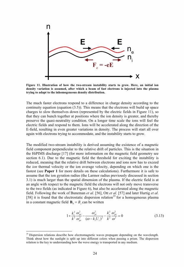
Figure 10. A ball resting in an unstable equilibrium. A small perturbation will make it roll downhill. The most central part of this work is related to anomalous transport (a fast transport of charged species) in conjunction with plasma instabilities. This is because the instabilities can affect the resistivity in the plasma and thereby the momentum transfer between electrons and ions, which ultimately will affect the transport properties of the charged species in the plasma. In a series of measurements with different types of electric field probes (presented in Paper 1) it was found that the modified two-stream instability (MTSI) can grow in the HiPIMS plasma. This is why it is worth spending some time investigating the matter.
The modified two-stream instability is a special case of the two-stream instability, which is taken as a good starting point for our discussion. The two-stream instability grows in a non-magnetized plasma provided that the relative drift between electrons and ions exceeds the electron thermal velocity, i.e. ( )1 2
,e i e th eU u u u kT m= − > = [21, p. 214]. This relative motion results in a Doppler shift between the plasma frequencies of the electrons and ions. If the wave vector18, k, of the oscillations fulfills the condition ωpe – kU = ωpi, oscillations in the two distributions of particles will enhance each other and the instability will start to grow exponentially [55]. Here ωpe and ωpi are the angular electron and ion plasma frequencies. One way of looking at this is by considering a region of the plasma where there is a small ion density variation in the plasma, as shown in Figure 11 for the 1D case. At a certain moment a beam of electrons is injected into the plasma.
18 A wave vector specifies the direction of the propagating wave. It is also related to the wavelength.
24
x
neni
E
Fe = -eE
E
n
Figure 11. Illustration of how the two-stream instability starts to grow. Here, an initial ion density variation is assumed, after which a beam of fast electrons is injected into the plasma trying to adapt to the inhomogeneous density distribution.
The much faster electrons respond to a difference in charge density according to the continuity equation (equation (3.5)). This means that the electrons will build up space charges to slow themselves down (represented by the electric fields in Figure 11), so that they can bunch together at positions where the ion density is greater, and thereby preserve the quasi-neutrality condition. On a longer time scale the ions will feel the electric fields and respond to them. Ions will be accelerated along the direction of the E-field, resulting in even greater variations in density. The process will start all over again with electrons trying to accommodate, and the instability starts to grow.
The modified two-stream instability is derived assuming the existence of a magnetic field component perpendicular to the relative drift of particles. This is the situation in the HiPIMS discharge [17] (for more information on the magnetic field geometry see section 6.1). Due to the magnetic field the threshold for exciting the instability is reduced, meaning that the relative drift between electrons and ions now has to exceed the ion thermal velocity or the ion average velocity, depending on which one is the fastest (see Paper 1 for more details on these calculations). Furthermore it is safe to assume that the ion gyration radius (the Larmor radius previously discussed in section 3.1) is much larger than the spatial dimension of the plasma. If the electric field is at an angle with respect to the magnetic field the electrons will not only move transverse to the two fields (as indicated in Figure 6), but also be accelerated along the magnetic field. Following the work of Buneman et al. [56], Ott et al. [57] and later Hurtig et al. [58] it is found that the electrostatic dispersion relation19 for a homogeneous plasma in a constant magnetic field 0 yB=B can be written
2 2 2 22
2 2 2 2 21 0( )
pe pi y pez
ge z z
kkk k U k
ω ω ωω ω ω
+ − − =−
(3.13)
19 Dispersion relations describe how electromagnetic waves propagate depending on the wavelength. Think about how the sunlight is split up into different colors when passing a prism. The dispersion relation is the key to understanding how the wave energy is transported in any medium.

25
where ωge is the angular electron gyration frequency (sometimes called the cyclotron frequency). Uz is the relative velocity and ki is the wave vector along i. One important case is propagation along the angle *θ of equal effective mass. It is the angle between the wave vector and the normal to the magnetic field, where the ions and electrons appear to have the same mass when subjected to an electric field, or written as */ sinm M θ= (3.14) The growth rate of the instability at *θ has been found to be max / 2lhγ ω= , where
/lh eB mMω ≈ is the lower hybrid frequency. This is another type of plasma oscillations, which is usually in the MHz regime for HiPIMS plasmas (see Paper 1). The instability gives rise to a sheared drift of electrons across the magnetic field lines (violating the frozen-in condition 20 [ 59 ] on very short timescales) directed momentarily by the direction of the oscillating electric field. Thus, the MTSI would be the driving mechanism behind the cross-B drift generating electric field oscillations in the lower hybrid regime. The energy from the relative drift between the charged species is used to excite the instability and oscillation energy is gained at the expense of the drift energy [21, p. 209]. Worth noting is that the lower hybrid frequency is somewhere between the gyro frequencies for ions and electrons meaning that it will affect both types of charged species, unlike for example high-frequency oscillations near the electron plasma frequency, which cannot affect the motion of the heavy ions. This will have interesting consequences when we now turn to discuss the anomalous transport of charged species.
3.6 Anomalous transport We are now ready to connect the parts on diffusion, resistivity and plasma instabilities and be able to draw some rather fascinating conclusions regarding the transport of charged species in pulsed plasmas (of which the HiPIMS plasma is one example). In the previous sections we found that the classical resistivity (eq. (3.9)) can be modified by a wave resistivity (eq. (3.12)) due to the existence of the modified two-stream instability. Furthermore, it was seen that the product ge EFFω τ between the electron angular gyro frequency, geω , and the effective electron momentum transfer time (also called the effective electron collision time), EFFτ , is a key parameter when it comes to determining how fast the cross-B diffusion really is for any given situation. The good news is that this wave resistivity can, in the case of for example magnetron discharges where the current is driven by an electric field, be found from a macroscopic measurement of the current density ratio / DJ Jϕ . Here Jϕ is the azimuthally rotating current density above the circular magnetron seen in Figure 12 and DJ the discharge current density running perpendicular to the magnetic field lines 20 Essentially it states that in a perfectly conducting fluid the magnetic field lines move with the fluid. This means that motion along the field lines do not change the field but motions transverse to the field carry the field with them.

26
(Figure 21). That this is true is seen in the following expression of the ratio between the Hall and Pedersen conductivites21 ( Hσ and Pσ ) [ 60, p. 50]:
2 2
2 2
2 2
1
1
ge EFFe
ge EFFHge EFF
ge EFFD P e
ge EFF
enEBJ E
J E enEB
ϕ
ω τω τσ ω τ
ω τσω τ
⋅ ⋅+
= = =⋅ ⋅
+
. (3.15)
In HiPIMS and mid-frequency pulsed magnetrons, recent measurements in different devices (see Paper 1 and references 17 and 61) agree on a value close to / ~ 2DJ Jϕ , which is roughly an order of magnitude lower than what is expected from classical theory of diffusion and electrical conductivity using collisions to move electrons across the magnetic field, or Bohm diffusion (8 30DJ Jϕ< < ) [17, 18, 62]. To sum up the results so far it can be concluded that a low ratio of / DJ Jϕ (or equivalently a low ge EFFω τ ), increases the transverse resistivity and thereby increasing the cross-B diffusion of electrons. This is why Paper 5 is dedicated to measuring the current density ratio, since it directly gives us a link to understand the charged particle transport in our plasma discharges. Last we will look at how the anomalous electron transport affects the ions, which was studied in Paper 2. From the equation of the macroscopic wave resistivity (eq. (3.11)) it can be seen that we would modify our classic picture of cross-B transport provided that there is a correlation between the oscillating density and electric wave field. In Paper 1 it was found that there indeed is an oscillating electric wave field and that the currents present in the HiPIMS discharge drives the MTSI. From earlier work on the same instability, where the same type of anomalous transport was detected, it was also found that variations in the plasma density were correlated to the electric field oscillations [53]. Due to this correlation, the waves give a net force ˆei eeE nϕ=F φ from the electrons to the ions, in the azimuthal direction (see Figure 12). Therefore a cross-field ion transport directed tangentially outwards in the HiPIMS discharge is expected.
21 Conductivity is a measure of a material's ability (in this case the plasma) to conduct an electric current. Hall conductivity is for the direction perpendicular to both the magnetic and electric fields (in the direction of E×B), while the Pedersen conductivity is for the direction perpendicular to the magnetic field and parallel to the electric field (cross-B).

27
Jφ
JφJφ
Eφ
EφEφFei
Fei
Figure 12. Illustration of the cross-field ion transport when facing the circular magnetron. Fei is the force on the ions, Jφ the azimuthal current density, and Eφ is the oscillating electric wave field, which is correlated to variations in plasma density, indicated by the grey and white stripes. Furthermore, since we now also have the possibility to look at the transverse resistivity from the point of effective collision time (eq. (3.12)), which governs how well momentum is transferred from the electrons to the ions, the situation can be formulated in a slightly different way: By investigating the forces involved in the charged particle transport it becomes clear that the azimuthal force on the ions,
ei een ϕη⊥= −F J , exerts a volume force on the ions tangentially outwards from the circular race track region. If the anomalous transport caused a decrease of / DJ Jϕ by an order of magnitude, then η⊥ would be expected to increase by an order of magnitude and thus increase the azimuthal force. As previously stated, it is therefore expected that the ions would be transported across the magnetic field lines and to a larger extent be deflected sideways, as shown in Figure 12.

28

29
4 Plasma Analysis
4.1 Background This chapter introduces the fundamentals of plasma diagnostics used in this work. It will by no means be a complete description of all techniques available, but rather a summary on the techniques used in the appended papers. In general, these techniques were used to characterize the plasma regarding dynamics and composition. Thus, they constitute a link between theory and experiments, and as such they are valuable tools in many plasma based processes. In thin film growth the information extracted from analyzing the plasma is important, since it tells us about the properties of the material flux transported in the plasma, which is often required in order to understand why coatings have certain properties (see for example reference 63 and 64).
4.2 Electrostatic probes For investigations of electric fields and oscillations in the plasma, electric probe arrays of different geometries were used in Paper 1, as seen in Figure 13.

30
Figure 13. Electric field probes and transformer used for measuring oscillations. (a) Impedance matching unit with connector sides. (b) Four-pin probe measuring Eρ and Eφ. The distance between the probe tips is 6 mm. (c) Fork-probe measuring azimuthal phase velocity, vφ. The distance between the probe tips is 4 mm. (d) Probe measuring Ez oscillations. The distance between the probe tips is 10 mm. The electric field is obtained from the difference in floating potential between pairs of cylindrical probe tips in the arrays. For accurate measurements, appropriate impedance matching is needed [65] and thus, two different impedance matching circuits, mounted inside the ceramic shaft of the probe, were used. In the study of the instability, oscillations in the MHz-range should be detected while filtering out the influence of the voltage pulse produced by the power supply22. It is easy to see how complicated this is by the following calculations: the amplitude of the electric field in our measurements is approximately 100 V m-1 and the distance between two probe tips is roughly 10 mm, resulting in a measured signal of 1 V. At the same time the HiPIMS voltage pulse might be up to 1 kV, which complicates matters substantially. For frequencies above 300 kHz a 40:1 transformer, wound on a ferrite toroid which transforms the 50 Ω of the oscilloscope to 80 kΩ was connected to the probes. For frequencies from tens of Hz up to a hundred kHz, this transformer has too low sensitivity and also too large phase shifts, so a conventional resistive divider of 10 kΩ/50 Ω was used instead. It has lower sensitivity at higher frequencies, but a flat low-frequency response (see Paper 1 for more details on the use of these probes).
22 Another feature is that this setup suppresses common-mode interference, which is a type of disturbance affecting both the signal and the signal return.

31
4.3 Magnetic probes There are many types of different magnetic probes that can be used to diagnose the plasma. A very popular type is the Rogowski coil, seen in Figure 14, which provides a way to directly measure the total alternating current (AC) flowing through its center [66, p. 15-17]. In Paper 5 such a probe was used to determine the internal currents in the HiPIMS plasma. The probe consists of a helical coil of wire with the lead from one end returning through the centre of the coil to the other end, so that both terminals are at the same end of the coil (back winding). Each turn of the Rogowski coil produces a voltage proportional to the rate of change of the magnetic flux through the turn. Assuming a uniform magnetic field density throughout each turn, the rate of change of the magnetic flux is equal to the rate of change of magnetic field density times the cross-sectional area for each turn. For a coil with n turns this results in
coild dBV n nAdt dtφ
= = . (4.1)
The magnetic field due to a long conductor carrying current is calculated through Ampère’s law
00 2l
II Br
μμπ
⋅ = ⇒ =∫ B dl , (4.2)
where r is the perpendicular radial distance from the conductor to the point at which the magnetic field is calculated. In combining the two equations above the total voltage of the probe is found to be
0
2coilnA dIV
r dtμπ
= . (4.3)
This probe signal is then integrated to yield the total current. It is not possible to measure DC currents with this type of probe, since the voltage that is induced in the coil is proportional to the rate of change of the current.

32
Figure 14. A Rogowski probe used in determining the internal currents in the HiPIMS discharge together with a sketch of the solenoidal coil showing the internal structure of the probe. The Rogowski coil is made having no ferromagnetic material in the core unlike a standard current transformer. Since it has no permeable core, the coil cannot be driven into saturation, which means it can respond linearly to extremely large currents [67]. Being of low inductance it can also respond to very high frequency pulses.
4.4 Langmuir probes One relatively straightforward technique to determine plasma parameters, such as electron temperature and density, floating and plasma potentials is known as the Langmuir probe. It was introduced in 1923 by I. Langmuir [68], who later analyzed them in great detail together with H. Mott-Smith [69]. The assumption of this probe technique is that, unlike a large electrode surface affecting the plasma, the Langmuir probe is small producing only small local plasma perturbations. When performing the measurements the Langmuir probe is immersed in the plasma and biased positively or negatively with respect to ground to draw electron or ion current, respectively. The relationship between the bias voltage, VB, and the collected current is referred to as the current-voltage characteristic. Figure 15 shows a typical I-V characteristic, where Vp is the plasma potential and Vf is the floating potential.

33
Vp
Vf
ion saturation electronsaturation
Figure 15. A typical I-V characteristic for a Langmuir probe measurement. For VB = Vp the probe has the same voltage as the plasma itself and draws mainly current from the more mobile electrons. In Langmuir probe measurements this current is often designated as positive as seen in Figure 15. Increasing VB beyond this point (VB > Vp) means that more and more electrons are attracted and in most cases, depending on probe geometry, the electron saturation current will eventually be reached. If instead decreasing the current so that VB < Vp then electrons will be repelled. At the point where the bias voltage equals the floating potential, i.e. VB = Vf, the electron and ion currents to the probe are equal meaning that I = 0. For VB < Vf the recorded current starts to be dominated by ion current. Soon the ion saturation current will be reached. The magnitude of the ion saturation current is much smaller than the electron saturation current due to the greater mass of the ions making them less mobile. The analysis of the Langmuir probe data that was carried out in Paper 6 is based on work by Gudmundsson and Magnus [ 70 , 71 , 72 ], who use the Druyvesteyn formulation (see for example Lieberman and Lichtenberg [20, p. 189] for a more thorough description) to extract not only the electron density and effective electron temperature, but also the electron energy distribution function (EEDF), ( )eg V , from the recorded I-V curves. By obtaining the first and second derivatives of the I-V curves it is possible to both get: 1) The plasma potential by identifying the maximum of e BdI dV as well as 2) the EEDF itself, which is found by
( )1 2 2
2 2
2 2 ee
d Im eVg Ve A m dV
⎛ ⎞= ⎜ ⎟⎝ ⎠
. (4.4)
Here Ie is the electron current and A is the probe area. From eq. (4.4) it is possible to
calculate the electron density through the change of variables 21
2mv
eε = according to
34
0
( )e en g dε ε∞
= ∫ , (4.5)
as well as the average energy
( )0
1e
e
g dn
ε ε ε ε∞
= ∫ . (4.6)
From the average energy the effective electron temperature can be calculated
according to Godyak [73] as 23effT ε= .
The Druyvesteyn approach works well also when measuring non-Maxwellian distributions [20, p. 191], which is often found in HiPIMS plasmas due to a highly energetic tail of electrons [74, 75]. Furthermore, it has also been shown that the EEDF is insensitive to the ratio of the probe dimensions to the Debye length [76, p. 95-134], which often is required in order to assume collision-less sheath conditions. Following the work of Kagan and Perel [77] it is seen that the above described method is suitable for cylindrical Langmuir probes, which were used in Paper 6. On the other hand it is necessary to verify that the electron collection at the probe tip is not distorted by the magnetic fields present in the magnetron discharge. In other words it is required that the electron Larmor radius, or often called gyro radius, rL, is greater than the probe radius (see section 3.1 for more details on the motion of a single electron). The electron Larmor radius is defined as
LmvreB
⊥= , (4.7)
where v⊥ is the electron velocity perpendicular to the magnetic field, which is (close to the cathode region, where the magnetic field is the strongest) calculated according to
1 2
02eVvm⊥
⎛ ⎞= ⎜ ⎟⎝ ⎠
. (4.8)
As previously V0 is the cathode potential. For the typical HiPIMS case using an upper limit for the magnetic field strength of 50 mT and a discharge voltage of 1 kV, we find that 2Lr ≈ mm. Worth noticing is that electrons of lower energies will of course have a considerably smaller Larmor radius. An electron with 2.5 eV will for example have a radius of 0.1 mm. In Paper 6 a tungsten wire of radius 0.0625pr = mm was used, meaning that the magnetic field only has a small perturbing effect on the Langmuir probe measurements. Still, for low electron energies and/or very close to the target race track we are approaching the limit of applicability of the small probe regime.
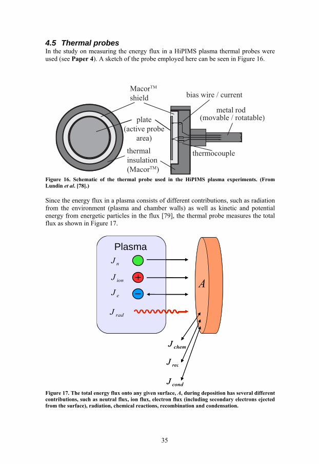
35
4.5 Thermal probes In the study on measuring the energy flux in a HiPIMS plasma thermal probes were used (see Paper 4). A sketch of the probe employed here can be seen in Figure 16.
bias wire / current
metal
thermalinsulation(MacorTM)
MacorTM
shield
plate(active probe
area)
Figure 16. Schematic of the thermal probe used in the HiPIMS plasma experiments. (From Lundin et al. [78].) Since the energy flux in a plasma consists of different contributions, such as radiation from the environment (plasma and chamber walls) as well as kinetic and potential energy from energetic particles in the flux [79], the thermal probe measures the total flux as shown in Figure 17.
A
J n
J ion
J e
J rad
J cond
J rec
J chem
Plasma
A
J n
J ion
J e
J rad
J cond
J rec
J chem
Plasma
Figure 17. The total energy flux onto any given surface, A, during deposition has several different contributions, such as neutral flux, ion flux, electron flux (including secondary electrons ejected from the surface), radiation, chemical reactions, recombination and condensation.

36
The principle for measuring the total energy flux with this type of probe has been described in Paper 4, but will also here be given for completeness. These type of measurements are based on the rate of change in temperature of the probe surface,
SdTdt
, which implies monitoring the temperature dynamics on the probe surface during
the heating process (plasma-on phase) as well as during the cooling (plasma-off phase), which is seen in Figure 18 [80].
0 20 40 60 80 100 120 14045
50
55
60
65
70
Sub
stra
te te
mpe
ratu
re, T
S [
°C ]
Time [ s ]
HeatingCooling
Figure 18. Temperature characteristics from a calibration of the thermal probe used in Paper 4 displaying a heating and cooling curve. The change of enthalpy of the substrate can be described by
SS
dTH Cdt
= (4.9)
where CS is the absolute heat capacity of the probe surface including the connected wires. The power balance during the heating process can be described by [81] heat in outH P P= − (4.10) and during the cooling process by cool outH P= − . (4.11) If we now assume that the incoming power, Pin, is constant during the heating process and the heat loss, Pout, is only a function of TS, then for each temperature, T , measured during the heating and the subsequent cooling of the probe surface the incoming power can be calculated by subtracting eq. (4.11) from eq. (4.10) such that

37
( ) S Sin heat cool ST
heat cool T
dT dTP T H H Cdt dt
⎡ ⎤⎛ ⎞ ⎛ ⎞⎡ ⎤= − = −⎢ ⎥⎜ ⎟ ⎜ ⎟⎣ ⎦ ⎝ ⎠ ⎝ ⎠⎣ ⎦. (4.12)
Furthermore, if the slopes of SdTdt
are determined under the condition that the
measurement starts and ends at equilibrium temperature (in our case room temperature) along with the exact knowledge of the heat capacity, then Pin can easily be determined. The total energy flux is thus obtained by dividing Pin by the probe surface area. Last, the heat capacity, CS, can be estimated by applying a known power to the probe surface e.g. by using a laser [82].
4.6 Mass spectrometry In order to characterize the different elemental species in the deposition flux other techniques are needed than the previously discussed probes. In this work, a method known as mass spectrometry was employed to look at the energy distributions of different ions present in the plasma. The setup is as follows (a more detailed description can be found in reference 83, chapter 4): An extraction probe with a small orifice is inserted into the plasma, into which gas atoms and ions enter. The mass spectrometer uses both electric and magnetic fields to filter incoming ions with respect their energy as well as mass-to-charge ratio. This also means that when studying neutrals, they first have to be ionized. By activating an ionization stage situated inside the extraction orifice consisting of a hot filament ejecting electrons, the neutral atoms become ionized through impact ionization (see also section 3.3). There are different types of filters used to filter out ions depending on their energy. The instrument used in Paper 2 was an energy-resolved mass spectrometer and a Bessel box was utilized [84]. It is a rather simple construction, which consists of electrodes that retard and focus the incoming ions, and thereby letting ions of a certain energy pass [85]. The final stage in the filtering process is a mass filter, and the most commonly used type is called a quadrupole mass filter [86, p. 88]. It uses four parallel electrodes onto which a constant (DC) plus a time-varying (AC) potential are applied. For given DC and AC values the ion trajectories through the electrodes will vary depending on the mass-to-charge ratio, in a way that only the desired ions will pass the filter while the others will be deviated from their original path. Finally the ions will be detected with a secondary electron multiplier (or a Faraday cup) and counted for in the included software.

38

39
5 Plasma modeling
5.1 Background Much can be said about plasma modeling and, as we will see, there is seldom a unique solution to the modeling problem. In general, models of plasma discharges can be highly valuable, since they allow us to test theory and fundamental mechanisms, which can be compared with experimental results. By running the models it is possible to get insight into the key plasma parameters, which sometimes can be extremely difficult to measure, and ultimately optimize the discharge itself through improvements of the experiment. One simple approach is to look at the plasma as a single fluid and then to introduce collisions so as to be able to model the interaction between the different particles. In this case it is assumed that the plasma can be described using a limited number of average parameters, such as mean velocity, density, temperature and pressure [87]. In the case of magnetron plasmas this requires that the sputtered material has undergone “enough” collisions to be thermalized with the surrounding plasma neutrals [88]. Calculating the mean free path for different species in order to see whether a particle will undergo a collision or not for a given distance will be done later on in this chapter. These rather crude approximations have been found to provide a surprisingly good description of different phenomena in the plasma [89, chapter 4]. In the case where there are very few particle collisions in the plasma, for example for high-energy electrons, it is not possible anymore to talk about average quantities characterizing the process, since we are no longer in thermodynamical equilibrium. This means that the concept of particle velocities having a Maxwellian distribution with a single temperature has to be abandoned (see also section 2.2). Instead it is necessary to introduce a more detailed representation of the plasma behavior, which can be found by a description using the six-dimensional (r, v) space in what is called kinetic theory23. In such a theory the behavior of the different species present in the plasma is described by statistical distributions of their positions and velocities given by the distribution function ( ), ,f tr v , which is the density of particles in (r, v) space at time t. We will here not dwell any longer on the kinetic approach, but merely show that the connection between the kinetic and fluid theories lies in taking the moments
23 Of course there is always the possibility of tracking every single particle in the plasma using Maxwell’s equations given in section 3.1. However, this is a far too complicated approach requiring tremendous computational power.

40
of ( ), ,f tr v , i.e. integrating the distribution function over the velocity coordinates, to retrieve the average quantities for the fluid description:
( ) ( ), , ,i in t f t d∞
−∞= ∫r r v v (5.1)
( ) ( ) ( )1, , ,,i i
i
t f t dn t
∞
−∞= ∫u r v r v v
r, (5.2)
where ( ),in tr is the average density and ( ),i tu r is the mean velocity of all particles of type i [89, chapter 12]. Knowledge of the distribution function is clearly vital and allows us to calculate the plasma parameters. One way of obtaining the distribution function for the electrons is through Langmuir probe measurements, described in section 4.4. In summary, fluid and kinetic theories can respectively be identified as macroscopic and microscopic models of the plasma. In this work the fluid approach was used in Paper VII in order to look at the process of ionization of sputtered materials. This is why we need to look further into the details of such a model.
5.2 Global models The modeling work presented in this thesis is a new, time-dependent (zero-dimensional) plasma model based on works by Ashida et al. [90], Hopwood [91], and Gudmundsson [92]. The working principle is a set of balance equations tracking the production and loss of different particles in the plasma. In this thesis we have focused on the gas particles present: Ar neutrals (Ar), Ar ions (only Ar+) and Ar metastables (Ar*). Furthermore, the metal neutrals (M) as well as metal ions (M+) together with the electrons (e-) were also accounted for. This means that the following plasma reactions were taken into consideration as displayed in Table 1. Reaction Description
*Ar e Ar e − −+ → + Excitation of Ar to metastable level +Ar e Ar 2e − −+ → + Electron impact ionization of Ar
*Ar e Ar e − −+ → + De-excitation of metastable Ar atoms * +Ar e Ar 2e − −+ → + Ionization of metastable Ar
+M e M 2e − −+ → + Electron impact ionization of M +M Ar M Ar ++ → + Charge exchange
Table 1. Plasma reactions taken into account in the global model. Penning ionization ( *Ar M Ar M e+ −+ → + + ) was not taken into account, since it is expected to be a negligible process during the HiPIMS discharge [92]. To set up the equations for the rate of change of the different species it is necessary to know the reaction rates, reactionk . For the work presented in Paper VII these were taken from Hopwood [91], Lee et al. [93, 94], and calculated from the electron impact ionization cross sections given by Freund et al. [95]. One simple example of how the density of metal ions changes in time can thereby be modeled as:

41
,
Mmiz e M chexc Ar M wall M M
dnk n n k n n k n
dt+
+ ++= + − , (5.3)
where the rates for electron impact ionization, charge exchange and loss of ions to chamber walls describe the different processes taking place. Furthermore, the electron density is found directly from the ion densities by assuming charge neutrality. The electron temperature is followed using a differential equation taking account of the energy exchange with other particles and the input power, hence called the power balance. This equation has essentially three contributions: 1) The external electrical input power, 2) the total electron energy loss due to collisions, and 3) surface losses (particles leaving the modeled plasma region). Furthermore, the model uses an experimentally determined time profile for the electrical power input. The fraction of the power assumed to be deposited in the ionization region is determined by matching the experimentally measured input current to the calculated total ion current to the target. The result can be seen in Figure 19. This is an approach, which takes into consideration the fact that there is a large potential drop over the cathode sheath. Physically it means that ions are accelerated to the target in the sheath region, and deposit energy there.
Time [ μs ]
Cur
rent
[ A
]
Figure 19. Comparison between the experimental current curve used as input in the global model and the calculated ion current to the target. In order to get a feeling for the rate of ionization it is often instructive to calculate the ionization mean free path for a given neutral atom travelling in the discharge plasma. This was done in Paper 7 for various metal atoms as well as for argon and it was found to be on the order of 1 cm for the HiPIMS discharge, meaning that an ionizing event is likely to happen here since the plasma region is of the order of tens of cm. As a comparison, in a typical DCMS discharge the ionization mean free path is approximately 50 cm [96] resulting in considerably less ionization (see sections 6.2 and 7.2 for more details on the difference between HiPIMS and conventional

42
magnetron discharges). For more details on the specific differential equations used see Paper 7 and reference 92. The loss of particles across bounding surfaces is most easily described by recalling the discussion on diffusion, where the simple case was that particles in high-density regions will diffuse towards regions of lower-density (section 3.4). The same situation is true for the ions also, where the ion density is quite small at the edge of the plasma. This is why terms including wallk will be present. At the same time there is of course also an influx of neutral gas (refill), which is treated as a diffusion process that would exactly balance the Ar diffusion losses if the Ar density and temperature equals the (pre-defined) background density. Finally, the global time-dependent plasma model was employed to estimate the degree of ionization of Ar as well as the sputtered metal, ( )i i nn n n+ , depending on electron density and target material for a typical HiPIMS discharge. Here, in is the metal ion density and nn the metal neutral density. An example of such a result is shown in Figure 20.
Figure 20. Estimated degrees of ionization for argon (Ar) as well as for the sputtered metal during a typical HiPIMS discharge. The metal was in this case titanium (Ti). Notice that the curve for Ar has been amplified ten times. It is important to keep in mind that the background gas is often much denser compared to the sputtered material density, which is why we only have a few percent degree of ionization in the case of Ar compared to Ti.

43
6 Magnetron sputtering
6.1 Background In the late 1930s Penning invented a way to better confine electrons near a surface by using electric and magnetic fields, resulting in increased ionization of the plasma in the vicinity of the surface. The Penning discharge was a first step towards the construction of a magnetron24 [97]. In the 1970s and 1980s variations of Penning’s invention was developed by several researchers, notably Penfold and Thornton [98] and later on Mattox, Cuthrell, Peeples and Dreike [99]. These new magnetrons allowed sputtering at lower pressures (~ mTorr) and lower voltages (~ 500 V), while having higher deposition rates than what had previously been attained using DC sputtering without magnets. The reason for the magnetron being excellent in confining the plasma is the magnetic field configuration combined with an electric field, such as the one generated by applying an electrical voltage. One example is where the magnets are placed with one pole positioned at the central axis of a circular magnetron, and the second pole placed in a ring configuration around the outer edge, as displayed in Figure 21.
24 Actually the first types of magnetrons were not used for material processing, but instead for generating microwaves in radars. These were called cavity magnetrons and were developed in the 1920s. Today we find these magnetrons inside all microwave ovens.
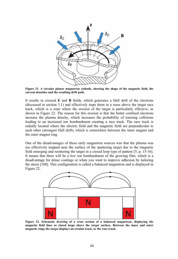
44
JDJD
z
Jφ
B
Figure 21. A circular planar magnetron cathode, showing the shape of the magnetic field, the current densities and the resulting drift path. It results in crossed E and B fields, which generates a Hall drift of the electrons (discussed in section 3.1) and effectively traps them in a torus above the target race track, which is a zone where the erosion of the target is particularly effective, as shown in Figure 22. The reason for this erosion is that the better confined electrons increase the plasma density, which increases the probability of ionizing collisions leading to an increased ion bombardment creating a race track. The race track is radially located where the electric field and the magnetic field are perpendicular to each other (strongest Hall drift), which is somewhere between the inner magnet and the outer magnet ring. One of the disadvantages of these early magnetron sources was that the plasma was too effectively trapped near the surface of the sputtering target due to the magnetic field emerging and reentering the target in a closed loop type of pattern [5, p. 15-16]. It means that there will be a low ion bombardment of the growing film, which is a disadvantage for dense coatings or when you want to improve adhesion by tailoring the stress [100]. This configuration is called a balanced magnetron and is displayed in Figure 22.
NN N
Figure 22. Schematic drawing of a cross section of a balanced magnetron, displaying the magnetic field lines as closed loops above the target surface. Between the inner and outer magnetic rings the target displays an erosion track, or the race track.

45
Instead it was the invention of the unbalanced magnetron by Window and Savvides in 1986 that offered a better solution [101]. The unbalanced magnetron allows some electrons to escape from the confining E×B field and create plasma in regions away from the target surface, which ultimately leads to a better transport of charged particles to the substrate. A sketch of an unbalanced magnetron is shown in Figure 23. An additional feature with this configuration is that when the escaping magnetic field is linked to other unbalanced magnetron sources (north to south poles) the plasma generation area can be significantly increased. This is called a closed-field magnetron configuration [102, 103], which is actually the opposite of what was investigated in Paper 6 (see also section 9.6).
NNN
Figure 23. Schematic drawing of a cross section of an unbalanced magnetron, displaying the magnetic field lines as only partially closed loops above the target surface. Here, the electrons can more easily escape and travel towards the substrate region.
6.2 Ionized PVD As we have come to understand, magnetron sputtering is an important industrial process for many applications ranging from deposition of hard coatings to deposition of functional coatings for electronic applications. Due to increasing demands from industry there is a constant need for improved coatings. It has led to a continuous effort in developing new and better sputtering techniques in order to tailor and enhance properties like hardness, wear and corrosion resistance, as well as specific electrical and optical behavior. One such possibility is direct control over the sputtered flux through increased ionization of the sputtered material [104]. Another advantage is that bombarding ions can transfer momentum to the surface atoms of the coating, which in turn leads to increased adatom25 mobility [10, p. 803]. This has beneficial consequences for the microstructure of the thin film [ 105 ] regarding enhanced mechanical and chemical properties. However, in glow discharge processes such as magnetron sputtering it is relatively easy to achieve a large fraction of gas ions (like Ar+), whereas ions from the sputtered metal are rare [106, 107, 108]. For many applications it is desired to increase the amount of metal ions, since this means
25 An adatom is an atom that has arrived and lies on the surface of the growing film.

46
greater control of the deposition flux in terms of direction and energy. One example is the use of a negative potential on the substrate for deposition of thin films into vias and trenches, where a neutral flux would tend to cover the upper part of the walls while leaving the bottom only partly covered [12]. When the deposition flux reaching the substrate consists of more ions than neutrals the process is referred to as ionized PVD, or IPVD [109]. There are many different IPVD-techniques available today. Some techniques increase the ionization of the atoms by post-vaporization ionization using plasmas and magnetic coils to generate ions that can be accelerated to the substrate surface when applying a negative bias [107]. Another technique is the previously mentioned cathodic arc evaporation (see for example references 110 and 111 ), which uses the fact that very localized; extremely high current discharges can create a dense plasma resulting in a high degree of ionization around a particular spot. A third possibility is the use of hollow cathode magnetron sputtering [112, 113]. The hollow cathode traps electrons in a hollow cylinder or between two parallel plates. It works like two electrostatic mirrors reflecting electrons between the sheaths until they are thermalized through collisions, and thus increasing the plasma density and the probability of ionizing any material passing through [114]. In summary it is clear that the perspective of having advantages like: improvement of the film quality by denser films [ 115 ] and enhanced adhesion, decreasing the deposition temperature [116], and better control over the deposition flux, is more than enough reason to continue developing new IPVD techniques. It is in this light that high power impulse magnetron sputtering (HiPIMS) has become so interesting, and is used as the main process in this thesis.

47
7 HiPIMS
7.1 Background High power impulse magnetron sputtering (HiPIMS), or sometimes referred to as high power pulsed magnetron sputtering (HPPMS), is an ionized PVD method based on conventional direct current magnetron sputtering (DCMS). As discussed in the previous chapter very little of the sputtered material in these conventional magnetron discharges is ionized, since the plasma power density is not high enough (or simply speaking that the electrical discharge power is not high enough). We will below come to understand that by increasing the power density will on one hand increase the plasma density and ionize more of the sputtered material, but on the other hand eventually melt the target, which of course is a less desirable effect. Instead, by applying very high power in repeated, short pulses, the average power is kept low enough for the cooling system to keep the target temperature below the melting point [12]. The technique of using pulsed plasma discharges on a conventional sputtering source was investigated by several researches such as Mozgrin et al. [13], Bugaev et al. [14] and Fetisov et al. [15], in the mid 90s, but it was not until Kouznetsov et al. published the much cited work on a new pulsed power magnetron technique in 1999 [12] when the concept of HiPIMS was spread to researchers in the field.
7.2 Fundamentals of HiPIMS There are several advantages inherent to the HiPIMS process of which a few will be discussed here. First of all, it is very easy to set up if a conventional magnetron sputtering system is present. In principle, all you need to change is the power supply making it possible to deliver high power pulses to the magnetron in the range of a few kW cm-2 while keeping the time-average power on a DCMS level of typically W cm-2 [35]. Such a HiPIMS discharge pulse can be seen in Figure 24. The particular length of the pulse is often kept in the range 10-500 μs [32, 117] with a pulse frequency from tens of Hz to several kHz [109, 118]. The voltage during the pulse is in most HiPIMS processes usually around 500-1000 V and the peak current density reaches a few A cm-2 (see for example reference 119).

48
Figure 24. A typical voltage-current plot on a HiPIMS discharge. The plot is taken from the investigation on gas depletion in Paper III, where a Cr target was used. The current density is about 1 A cm-2. Furthermore, a large fraction of the sputtered material is ionized resulting in denser films [120, 121], since the ion flux enhances surface mobility of the adatoms and thereby reducing film porosity (see reference 105 and Paper 7). The reason why material (metal) ions are so abundant has to do with the above mentioned high power density in the HiPIMS discharge, which causes a tremendous increase of charge carriers as the voltage is increased (see section 2.2 on discharge characteristics). In numbers this means that the electron density in the ionization region close to the target surface is on the order of 1018-1019 m-3 [122, 123]. For an electron density around 1019 m-3 the ionization mean free path is about 1 cm (see section 5.2), while for an electron density of 1017 m-3, commonly observed in a DCMS discharge, the ionization mean free path is approximately 50 cm for typical discharge conditions [96]. Thus, given the high electron density in the HiPIMS discharge we would expect a significant fraction of the sputtered material to be ionized, which also has been verified in a great number of publications [12, 124, 125, 126]. On the other hand, there are differences in the degree of ionization of the sputtered material depending on what material is used (a couple of percent to almost fully ionized depending on material [125, 127]). As we previously saw in chapter 5 on plasma modeling this has to do with the ionization rate of the material, which largely depends on the electron impact cross section in the HiPIMS regime [92] as well as the ionization potential varying from material to material (see for example 91 and Paper 7). Still, it is safe to conclude that the HiPIMS discharge is an IPVD technique resulting in a large flux of ionized sputtered material. Also worth mentioning is that the presence of multiply charged ions of some sputtered materials such as Ti and Al (but not C) has led to the onset of self-sputtering regimes characterized by a second increase of the current beyond the value of the initial peak current, if the pulse is sustained for a long enough time in combination with high negative discharge voltages [128, 129]. The sustained

49
self-sputtering has been proposed to be due to secondary electron emission caused by the multiply charged material ions (potential emission), which are accelerated in the target sheath [128]. The singly ionized sputtered atoms can not contribute to this process, since they often do not exceed the ionization energy threshold and the subsequent release of secondary electrons into the plasma. This has led to the possibility that HiPIMS processes can be run without the use of a process gas, which opens up the field of ultra-clean sputtering [130]. So far we have seen that sputtered material is abundantly ionized and we will now turn to discuss that by varying the substrate bias voltage the direction as well as the energy of the ionized deposition flux can be tailored for certain purposes. This is because charged species can be accelerated and guided in the deposition chamber by using electric or magnetic fields. It means that HiPIMS is a suitable technique for coating complex shaped surfaces, where sometimes the film growth will be perpendicular to the initial flux from the target surface, and thus making the process suitable for e.g. trench filling applications in the semiconductor industries [12]. These ideas were nicely demonstrated by Alami et al. [120] using electric fields (substrate bias) to deposit the sidewall of a trench and by Bohlmark et al. [131] using magnetic fields to guide the ionized material. The same principles were combined with the findings on anomalous charge transport in HiPIMS (Paper 1 and 2 as well as section 3.6) to coat for example the inside of tubular objects, investigated in Paper 6. Another advantage of generating a large fraction of ions in HiPIMS is the possibility of using it for surface pretreatment. Here bombarding ions sputter away oxide layers existing on most material surfaces and thereby cleaning the substrate prior to deposition. During the process some ions are also implanted in the substrate. This results in a gradual change in composition between the substrate and the film grown on top. Pre-treatment of surfaces in this way has been shown to improve adhesion [121, 132] and thus enhance wear and corrosion properties [133]. Moreover, the HiPIMS plasma generates large quantities of highly energetic ions [74]. From ion energy measurements in HiPIMS discharges it has been found that the average ion energy is around 20 eV without using any substrate bias (see reference 74 and Paper 2). As it turns out, ion energies in the range 20 – 30 eV have been shown to have a densifying effect on thin films [134], which is a very fortunate result. Finally, Table 2 sums up a few important parameters for the HiPIMS process. They are not to be seen as exact values, but rather a help to determine what type of discharge we are dealing with.
Parameter Value
Peak power density 103 W cm-2
Average power density 1 W cm-2
Current density 1-10 A cm-2
Discharge voltage 500-1000 V
Process gas pressure 10-3-10-2 Torr (0.1 – 1 Pa)
Magnetic field strength 0.010-0.100 T
Electron density 1018-1019 m-3

50
Electron temperature 1-5 eV
Ion energy (average for metal ions) 20 eV
Debye length 10-6-10-5 m
Electron gyroradius 10-4-10-3 m
Ion gyroradius 10-1 m
Electron gyrofrequency 109 Hz
Ion gyrofrequency 104 Hz
Lower hybrid frequency 106 Hz
Electron plasma frequency 109 Hz
Ion plasma frequency 108 Hz
Ionization mean free path 10-2 m
Table 2. A summary of important parameters for the HiPIMS discharge.
7.3 Challenges facing HiPIMS The lower deposition rate for HiPIMS compared to DCMS for the same average power is a drawback26, and is one of the most discussed topics in this field of research. In a review on HiPIMS by Helmersson et al. [109] it was found that the rates are typically in the range of 25-35 % compared to DCMS, which makes the technique less attractive for industrial use. Before going on and discussing situations where there is no issue with the deposition rate, let us first have a look at the ideas on why there sometimes is a reduction. Already discussed in the section on sputtering (section 2.4), Christie [30] suggested that the back-attraction of metal ions to the target followed by self-sputtering causes a reduction in the amount of sputtered particles reaching the substrate (Figure 5). Konstantinidis et al. [117] found that the amount of ions reaching the substrate is affected by the plasma conductivity, which was seen by creating a secondary plasma between the magnetron and the substrate using an external coil. Furthermore, Bugaev et al. [14] and Bohlmark et al. [131] showed that the magnetic confinement of the sputtered material affected the deposition rate. Emmerlich et al. [33] highlighted the non-linear energy dependence of the sputtering yield (discussed in section 2.4), meaning that it does not make sense to compare HiPIMS and DCMS deposition rates for the same average power if not taking this dependence into account. When comparing with experimental results they saw trends confirming their experiments, but it could not fully explain the differences. In this thesis the main focus has been to characterize and understand the transport mechanisms in HiPIMS, which led to the discovery of an anomalous transport of charged species (section 3.6). As we earlier saw, it resulted in an increase of ions being transported parallel to the target surface and lost to the walls instead of arriving at the substrate position, and thus reducing the deposition rate. It is most likely a combination of the factors mentioned above, and possibly others that affect the deposition rate. Also worth noticing is that the addition of a reactive gas, such as N2 or O2, in the HiPIMS process, has resulted in the opposite results. In this case, rates 26 One could also mention the risk of arcs, ejecting microdroplets out into the deposition chamber. With modern arc suppression units this is not considered to be a problem anymore.

51
equal to or even higher than for DCMS have been found in deposition of Al2O3 [118] and ZrO2 [135]. The reason for this is suggested to be increased process stability (reduction of hysteresis) as well as a high erosion rate during the HiPIMS discharge, which effectively cleans the target surface and thus displaces the onset of target poisoning27 to higher reactive gas flows. Furthermore, there are also many situations where the quality of the coating is far more important than the time it takes to produce that coating and one should, as always, be careful when making these comparisons based on only one or a few properties. In conclusion we see that the deposition rate is a complex matter, connected with a whole range of different parameters. This is of course also a major reason to why it is so interesting!
27 Target poisoning is compound formation on the target surface. Usually the compound has a higher binding energy compared to the pure metal, which dramatically decreases the deposition rate.

52

53
8 Thin film characterization
8.1 Background Throughout this thesis we have sought to test our ideas on how the HiPIMS plasma affects the growth of thin films. This has of course led us to deposit a fair number of coatings using several different targets (see for example Paper 2, 6 and 7). In order to analyze the end result, a few different thin film characterization techniques have been employed. As with the plasma analysis in chapter 4, this is by no means an exhaustive list of available techniques.
8.2 Scanning electron microscopy Scanning electron microscopy (SEM) is a popular material characterization technique used both in industry and academia. The reasons for this are several: the simplicity to use, where none or little sample preparation is required (the sample needs only to be conductive), and the SEM’s capability of producing images of high resolution as well as a large depth of field, which allows a large amount of the sample to be in focus at any given time. By using the SEM it is often possible to distinguish features on the scale of 10 nm [136, chapter 1].

54
Electron gun
Anode
Magnetic lens
Scanning coils
Stage with specimen
Backscatteredelectrons
Secondaryelectrons
Electronbeam
Figure 25. Schematic drawing of the SEM’s electron column showing the electron gun, lenses and deflection system. The SEM uses electrons instead of light to form an image. A beam of electrons is produced at the top of the microscope by for example heating a metallic filament (one type of electron gun), and attracted towards the anode [6, p. 585]. The electron beam follows a vertical path through the column of the microscope. It makes its way through electromagnetic lenses, which focus and direct the beam down towards the sample. The lenses also control the scanning procedure by moving the beam. This microscopy technique is operating under vacuum conditions, and usually we also find pumps located at the base of the column, producing a working pressure of around 10-4-10-3 Pa. Once the electron beam hits the sample it will generate backscattered and secondary electrons that are ejected from the sample. With a standard detector, such as the Everhart-Thornely detector or the Inlens detector both backscattered and secondary electron signals can be collected [136, chapter 2] giving information about the surface and the subsurface (a depth of a few angstroms) [6, p. 587]. Through amplification of the signal topographical images of the sample surface can readily be obtained. Furthermore, by cleaving the sample it is also straightforward to produce cross-sectional images, such as depicted in Figure 26. In this way the film thickness and microstructure were investigated in Paper 2, 6 and 7.

55
Figure 26. Cross-sectional SEM image of a Ti sample grown on top of a Si substrate using HiPIMS. The sample exhibits a smooth surface free of voids and large porosities. (From Paper 7.) The SEM can also be used to detect compositional information, since X-ray photons are emitted in the process. The technique is called energy-dispersive x-ray spectroscopy (EDX), which utilizes x-rays that are characteristic of an element's atomic structure to be identified uniquely from each other.
8.3 Ion beam analysis In many cases it is necessary to go beyond a high-resolution image of the sample and try to gain insight into the composition and elemental depth profiles in the near-surface layer of solids. By using ion beams in the MeV-range it is possible to do this and the common name for several of these techniques is ion beam analysis (IBA) [137, 138]. All IBA methods are highly sensitive and allow the detection of elements in the sub-monolayer range. The depth resolution is typically in the range of a few nanometers to a few ten nanometers. The analyzed depth ranges from a few ten nanometers to a few ten micrometers. Two different IBA methods, discussed here in more detail, are known as Rutherford backscattering (RBS) and elastic recoil detection analysis (ERDA) [139, chapter 3], which also have the benefit of giving reliable elemental quantification with an accuracy of a few percent without using any complex calibration (unlike for example EDX). Both these methods were used in Paper VII in order to obtain thin film surface densities [140] and the degree of contaminants present. In general RBS and ERDA are rather similar techniques. In RBS the ion beam is used to backscatter against atoms of the sample. The energy loss of these backscattered ions is then measured, after which mass and depth information can be obtained as seen in Figure 27.

56
E0
E1*
ΔEin
ΔEout
E1
Et Figure 27. A sketch of the incoming ion beam of energy E0 used in RBS. There is a gradual reduction of the particle’s kinetic energy as it traverses the sample, due to many small-angle scattering events (ΔEin and ΔEout). Eventually the particle will undergo large-angle scattering (Et), travel in the direction of E1 and finally be detected. For ERDA the ion beam instead knocks out atoms in the sample, and these recoil atoms are then detected. In time-of-flight ERDA, mass and depth information is obtained through a combination of measuring the energy of the recoiling atoms as well as their velocity resulting in a 2D spectrum [137]. RBS and ERDA are complementary techniques. RBS is suitable for detecting heavy elements using ion beams consisting of light ions such as He ions, while ERDA is better for light to medium atoms using a heavy ion beam such as I ions [141]. Both techniques have a good mass separation for lighter elements, but worse for heavier elements. In order to get a good mass resolution in RBS it is necessary to have thin samples, because thick layers of heavy elements may cause an overlap of detected light elements in the measured spectrum [137]. This means that it would be hard to detect the different constituents, which is seen in Figure 28.
Al
Si
Pb?
Figure 28. RBS measurement and simulation of an approximately 1 μm thick Al coating on a Si substrate. Al is lighter than Si and therefore shows up as a peak around 850 keV overlapped with the Si peak. In this measurement small amounts of impurities, possibly Pb, is detected around 1750 keV.

57
Furthermore, both methods require little sample preparation, and very small quantities of the sample are needed meaning sample areas of a few tens of mm2, and a thickness in the nm range. Both RBS and ERDA are non-destructive methods [142]. The time to run the analysis is relatively fast, and a spectrum can usually be obtained after 15 min for RBS and around 30 min for ERDA, if disregarding the time it takes to mount the samples and align the ion beam. The time consuming part is mainly the analysis of the measured spectrum, which is performed using a computer software, such as the SIMNRA 6.04 code [143]. Here it is important to have insight into what elements might be in the film, in order to make as good fitting as possible. This also means that both methods are good for quantification of known elements, but less suitable for unknown samples.

58

59
9 Summary of results
9.1 Paper 1 - Anomalous electron transport in high power impulse magnetron sputtering
In sections 3.5-3.6 a new type of anomalous transport operating in the HiPIMS regime was discussed in connection to changes in resistivity and plasma instabilities. It all started with measurements of magnetic field changes in HiPIMS discharges by Bohlmark et al. [17] done on the same experimental setup as used in this work. They found a surprisingly high speed of electron transport across the magnetic field lines during the HiPIMS discharge, which could not be explained by classical theory of diffusion and electrical conductivity, moving electrons across the magnetic field lines using collisions, or Bohm diffusion (described in section 3.4). As we saw in section 3.6, the degree of anomalous transport can be estimated by measuring the azimuthal current density, Jϕ , and the discharge current density, DJ , generated by cross-B transported electrons. By doing so, it is possible to calculate the current density ratio. In DCMS, measurements of / DJ Jϕ give typical values in the range 8 30DJ Jϕ< < [17, 18, 62]. In HiPIMS and mid-frequency pulsed magnetrons, recent measurements in different devices [17, 61]) agree on a value close to / 2DJ Jϕ ≈ (with an estimated error by a factor of 2), which is roughly an order of magnitude lower than for DCMS. Paper 1 was therefore dedicated to verifying the low current density ratio indicating faster-than-Bohm cross-B transport as well as trying to explain the underlying mechanisms behind this phenomenon. It was demonstrated that in HiPIMS discharges the Hall current was only one contribution out of three to the total azimuthal current. A more detailed analysis of the / DJ Jϕ ratio showed that the value / 2DJ Jϕ ≈ was indeed attained, in agreement with Bohlmark’s investigation [17] on anomalous electron transport in HiPIMS plasmas. Further investigations of the anomalous transport resulted in the discovery that this phenomenon could quantitatively be described as being related and mediated by highly nonlinear waves, likely due to the modified two-stream instability (MTSI), resulting in electric field oscillations in the MHz-range (the lower hybrid frequency, see section 3.5). Measurements in the plasma confirmed these oscillations as well as trends predicted by the theory of these types of waves. The results provided important insights into understanding the mechanism behind the anomalous transport.

60
9.2 Paper 2 - Cross-field ion transport during high power impulse magnetron sputtering
An important result of the theory of anomalous transport is that the current ratio / DJ Jϕ is inversely proportional to the transverse resistivity, η⊥ , which governs how
well momentum is transferred from the electrons to the ions (as described in more detail in section 3.6). An analysis of the forces involved in the anomalous particle transport showed that, besides an enhanced electron mobility, there is an azimuthal force on the ions, i eenϕ ϕη⊥= −F J , directed tangentially outwards from the circular race track region (see Figure 12). If the anomalous transport caused a decrease of
/ DJ Jϕ by an order of magnitude, then η⊥ would be expected to increase by an order of magnitude and thus increase the azimuthal force. It is therefore expected that the ions would be transported across the magnetic field lines and to a larger extent be deflected sideways, instead of solely moving from the target region towards a substrate placed in front of the target some distance away. The above presented theory was verified in two separate experiments consisting of: (1) a comparison between deposition rates on substrates placed perpendicularly near the side of the target surface and a reference substrate placed parallel in front of the target, and (2) an investigation of the ion energy distributions of the side-deposited ions. The measurements were performed for both HiPIMS and DCMS. It was found that a substantial fraction of sputtered material is transported radially away from the cathode and lost to the walls in HiPIMS as well as DCMS, but more so for HiPIMS giving one possible explanation to why the deposition rate on substrates placed in front of the target is lower compared to DCMS. Furthermore, ion energy distributions of sideways transported Ti+ measured in the HiPIMS plasma at different axial distances from the target race track clearly showed a high energy tail with ion energies above 20 eV. These results were only seen in the HiPIMS pulses and not in the conventional DCMS discharge, consistent with the much weaker (Bohm regime) cross-B transport. Important conclusions from this work were that the ion energy distribution measurements confirmed the theoretical model on anomalous transport, resulting in a previously neglected cross-B side-transport.
9.3 Paper 3 - Transition between the discharge regimes of high power impulse magnetron sputtering and conventional direct current magnetron sputtering
The different plasma properties seen in HiPIMS, such as a dramatic plasma density increase [122, 123], higher degree of ionization [12] and highly energetic ions [74], compared to DCMS were in this work investigated at the level of the discharge, since the current-voltage characteristics is the fundamental modification of these two processes. The aim of the study was to apply long enough HiPIMS pulses in order to identify similar steady-state conditions as achieved during DCMS. Two different current regimes could clearly be distinguished during the pulses: (1) A high-current transient followed by (2) a plateau at lower current. At high applied negative voltages the high-current transient had the characteristics of HiPIMS pulses, while at lower voltages the plateau values agreed with currents in DCMS using the same applied voltage. The current behavior was found to be strongly correlated with the chamber
61
gas pressure, where increasing gas pressure resulted in increasing peak current and plateau current. Based on these experiments and estimates of plasma transport and gas dynamics during the discharge, it was suggested that the high-current transients cause a depletion of the working gas in the area in front of the target, and thereby a transition to a DCMS-like high voltage, lower current regime. This loss of gas has previously been studied in magnetron discharges [37, 38], but then only related to gas rarefaction (see section 2.4), where the depletion of gas is mainly through collisional heating between the background gas and sputter-ejected target atoms as well as reflected sputtering gas atoms, followed by thermal expansion. In this work further mechanisms were taken into account, such as a direct loss of ionized gas, which is accelerated towards the target surface, then neutralized and still energetic enough to pass quickly through the near-cathode region. Furthermore, the importance of the gas refill mechanism was studied for different off-times which provided insight into the required time it takes for the influx of neutral gas to diffuse into the most intense area of the discharge. In conclusion it was found that the reduction of gas during HiPIMS processes can dramatically alter the discharge characteristics and thereby the resulting deposition conditions.
9.4 Paper 4 - Energy flux measurements in high power impulse magnetron sputtering
The investigation on energetic ions continued by measuring the total energy flux in the HiPIMS discharge using thermal probes (described in section 4.5). The reason for this work was that a large flux of highly energetic ionized material is often found to be detrimental to the growing film, since it may induce compressive stress as the bombarding species are distorting the lattice of the sputtered films [6, p. 748], which will eventually cause the film to peel off. Furthermore, the heating due to the energetic species present in the HiPIMS plasma [74] might melt thermally sensitive substrates, such as plastics. In this work it was found that the substrate heating is reduced in the HiPIMS process compared to DCMS at the same average power. This was explained by the lower deposition rate, which was estimated to about 20 % of the DCMS rate for Ti, resulting in fewer bombarding particles per time unit. When taking this fact into account it was concluded that approximately 90 % more energy per incoming particle is deposited on the substrate in the HiPIMS case. Moreover, by mapping out the total thermal flux in the radial direction (parallel to the magnetron surface) as well as the axial direction (perpendicular to the magnetron surface) it was seen that the heating due to radial energy flux reached as much as 60 % of the axial energy flux, which was likely a result of the anomalous transport of charged species present in the HiPIMS discharge, resulting in a strong cross-B side-transport of ionized sputtered material, as seen in Paper 2. Last, the electronic and ionic contributions to the energy flux were separated by using an applied bias to the thermal probe. The experimental results were compared to theoretical calculations on energy flux of charged species, and they were found to be in good agreement.
62
9.5 Paper 5 - Internal current measurements in high power impulse magnetron sputtering
The anomalous transport previously investigated in Paper 1 and 2 showed that the current density ratio, / DJ Jϕ , could characterize the transport present in the HiPIMS discharge for any given time. Up till this point it had not been possible to directly measure this ratio, but merely estimate a value based on measurements of the electric field. This problem was resolved in the present publication, where we used Rogowski coils, which, unlike electrical probes, require no further information regarding the plasma characteristics when determining the current density (see section 4.3). The new data indicated spatial and temporal variations of / DJ Jϕ during the HiPIMS discharge, governing the cross-B resistivity and also the energy of the charged particles. Based on these findings a phenomenological model was constructed, which describes the evolution of the current density in this type of plasma discharge. The core of the model is based on six different types of current systems, which characterize the operating transport mechanisms such as current transport along and across magnetic field lines, as well as the initiation, build-up and steady-state of a HiPIMS plasma. The previously reported faster-than-Bohm cross-B electron transport was verified in the experiments, but was not found to be present in the whole discharge volume. These results on the plasma dynamics contributed to ongoing HiPIMS modeling of for example the axial electric field distribution, governing the back-attraction of ionized sputtered material, and might furthermore provide a link between the different resistivities reported in HiPIMS, pulsed-DC, and DC magnetron discharges.
9.6 Paper 6 - Dual-magnetron open field sputtering system for sideways deposition of thin films
The cross-B side-transport of ionized sputtered material described in Paper 2 was investigated in a new type of deposition geometry, where the aim was to coat tubular and complex shaped surfaces, such as the interior of cylindrical shaped substrates. In the experiments an open-field co-axial dual-magnetron system was set up28 where two identical Ti targets were synchronously driven. The open-field configuration causes the plasma to follow the magnetic field lines and extend towards the side walls of the deposition chamber and thus facilitate the desired sideways transport. In this study we tried to optimize the growth conditions by changing the distance between the magnetrons, the process pressure as well as utilizing both DCMS and HiPIMS. It was found that the sideways deposition of high-quality films can be made at reasonable deposition rates. High electron densities of the order of 10-18 m-3 were determined by Langmuir probe measurements in the case of HiPIMS discharges, which in turn provided a high degree of ionized sputtered material as verified by optical emission spectroscopy. Furthermore, SEM investigations of the films grown at several positions perpendicular to the surfaces of the two magnetrons indicated no flaking or irregularities, and thus confirming the strength of this method.
28 This means that the magnetic field configuration is arranged in such a way that the field lines from one magnetron are not linked to the other, i.e. the polarity of the opposing magnetrons are identical.

63
9.7 Paper 7 - On the film density using high power impulse magnetron sputtering
Previous studies on transport of ions in the HiPIMS discharge showed highly energetic metal ions (see reference 74 and Paper 2), which were speculated to have a densifying effect on the film growth [120, 121]. Still there were no conclusive evidence (mainly due to lack of investigations) that this effect is a general trend, or how large improvement it might be, since the results varied from a few percent [119] to about 30 % [127]. This is why an in-depth study using eight different metallic materials (Al, Ti, Cr, Cu, Zr, Ag, Ta, and Pt) to investigate the densification process was performed in Paper 7. No compound materials were used in order to minimize the complexity of the system. The density values for the HiPIMS films were measured and compared with results from thin films grown under equivalent conditions using DCMS in addition to tabulated bulk values. The impurity content and its effect on the density were also analyzed using ion beam analysis (section 8.3) in order to get as good density values as possible. It was concluded that even at unfavorable deposition conditions (no substrate bias or additional heating) the HiPIMS films exhibited an overall ~ 5-15 % density increases compared to DCMS. By using a global plasma model to estimate the plasma conditions during deposition, the results could be attributed to the increased ion bombardment, leading to a less pronounced columnar microstructure [105, 134]. Furthermore, the deposition rates were found to be lower for HiPIMS compared to DCMS, as was previously discussed in section 7.3, but for several materials this decrease was not as pronounced as previously reported in the literature. This was shown in the case of Ta, Pt, and Ag with rateHiPIMS/rateDCMS ~ 70-85 %, while still achieving denser coatings.

64

65
10 Ongoing and future research
The world of plasma still remains to a great extent undiscovered, with big questions within the fields of fusion plasmas [144], space plasmas [145] and dusty plasmas [146] yet to be solved. As you might imagine, the combination of thin film deposition and plasma physics definitely leaves some room for new discoveries, although I have done my best to answer a few things in my research on HiPIMS.
One very important aspect of future work on HiPIMS is the theoretical modeling, which has so far been reasonably successful in verifying experimental results regarding particle transport, gas rarefaction, electrical field and potential distributions etc. In order to fully understand the underlying mechanisms operating in the HiPIMS discharge more work in this area is needed. In general, the question regarding how to handle processes that vary on sub-microseconds to seconds within the limit of computational power is yet to be answered. Remains to be decided is also how one should tackle the spatial differences, where global modeling is likely not accurate enough. Along this line of thought we are working on developing new HiPIMS models together with our colleagues at the Royal Institute of Technology in Stockholm. The results generated so far are very promising [147], but much work remains, in particular with benchmarking the simulations to experimental results from the HiPIMS community.
Another fascinating part of the HiPIMS process is the film growth. As has been shown in this work (and references herein) there are numerous results showing new and promising results regarding film quality. Many plasma-related phenomena have been discussed, but less is known when it comes to film growth using this technique. It is therefore time to go beyond the description of a high fraction of ionized sputtered material with an inherent high energy to include more details in order to fully characterize the growth mechanisms. The aim should be to connect the plasma characteristics, such as the dynamics of the different species present as well as the electromagnetic field profiles, to the growth process. In doing so, we will eventually be able to answer what type of pulse and discharge environment are required in order to generate certain growth conditions.
When we investigated the transport properties in HiPIMS plasmas, rotating spoke formations were discovered. This has previously been detected in other plasma experiments outside the field of thin film deposition [148, 149]. It would be highly
66
interesting to investigate this matter further and be able to characterize what happens. This could be another clue to the charged particle transport in HiPIMS.
The possibility of additional plasma characterization is far from exhausted. There is still a need to do correlated density and electric field measurements to fully characterize the cross-B transport. Furthermore the question on the degree of gas depletion taking place in the HiPIMS discharge, affecting both the discharge as well as the film growth, is not yet completely resolved. In this area, work has been carried out together with our colleagues at Université Paris-Sud, France, which shows promising results.
Finally, at the time of this thesis no “killer application” has to my knowledge been identified for HiPIMS. There are several interesting possibilities, such as reactive HiPIMS [118, 135], etch processes [133], denser coatings (Paper 7), ultra-clean sputtering [130] etc, but we have so far failed to unleash the full capability of this technology. Luckily the interest for HiPIMS is ever increasing [35] and I have great hopes for what is yet to come.
67
11 References
[1] E.D. Nicholson, Gold Bull. 12, 161 (1979) [2] P.L. Cavallotti Electrochimica Acta 50, 4523 (2005) [3] W.R. Grove, Phil. Trans. Royal Soc. 87, B142 (1852) [4] A.W. Wright, Am. J. Sci. Arts 14, 169 (1878) [5] D.M. Mattox, The Foundations of Vacuum Coating Technology, Noyes Publications / William Andrew Publishing, New York, USA (2003) [6] M. Ohring Materials Science of Thin Films, Academic Press, San Diego, CA, USA, (2002) [7] J.L. Vossen and W. Kern (eds.), Thin Film Processes II, Academic Press, New York, USA (1991) [8] J.E. Gray and B. Luan, J. Alloys Compd. 336, 88 (2002) [9] R. Reif and W. Kern in J.L. Vossen and W. Kern (eds.), Thin Film Processes II, Academic Press, New York, USA (1991) [10] K.S. Sree Harsha, Principles of Physical Vapor Deposition of Thin Films, Elsevier Science, Oxford, UK (2006) [11] H.F. Winters and E. Kay, J. Appl. Phys. 38, 3928 (1967) [12] V. Kouznetsov, K. Macák, J.M. Schneider, U. Helmersson, and I. Petrov, Surf. Coat. Technol. 122, 290 (1999) [13] D.V. Mozgrin, I.K. Fetisov, and G.V. Khodachenko, Plasma Phys. Rep. 25, 255 (1999) [14] S.P. Bugaev, N.N. Koval, N.S. Sochugov, and A.N. Zakharov, Proceedings of the XVIIth International Symposium on Discharges and Electrical Insulation in Vacuum, p. 1074, Berkeley, CA, USA, July 21-26 (1996) [15] I.K. Fetisov, A.A. Filippov, G.V. Khodachenko, D.V. Mozgrin, and A.A. Pisarev, Vacuum 53, 133 (1999) [16] V. Kouznetsov, U.S. Patent No. 6,296,742 B1 (2001) [17] J. Bohlmark, U. Helmersson, M. VanZeeland, I. Axnäs, J. Alami, and N. Brenning, Plasma Sources Sci. Technol. 13, 654 (2004) [18] S.M. Rossnagel and H.R. Kaufman, J. Vac. Sci. Technol. A 5, 2276 (1987) [19] I. Langmuir, Proc. Nat. Acad. Sci. U.S. 14, 627 (1928) [20] M.A. Lieberman and A.J. Lichtenberg, Principles of Plasma Discharges and Materials Processing, John Wiley & Sons, New York, USA (2005) [21] F.F. Chen, Introduction to Plasma Physics and Controlled Fusion Vol. I: Plasma Physics, Plenum, New York, USA (1984) [22] S.M. Rossnagel in J.L. Vossen and W. Kern (eds.), Thin Film Processes II, Academic Press, New York, USA (1991) [23] D.M. Sanders, J. Vac. Sci. Technol. A 7, 2339 (1989)

68
[24] J.R. Roth, Industrial Plasma Engineering Volume 1: Principles, Institute of Physics Publishing, Bristol, UK (1995) [25] F.F. Chen and J.P. Chang, Lecture notes on principles of plasma processing, Kluwer Academic/Plenum Publishers, New York, USA (2003) [26] S.R. Kasi, H. Kang, C.S. Sass, and J.W. Rabalais, Surf. Sci. Rep. 10, 1 (1989) [27] http://www.srim.org accessed 29 March 2010 [28] P. Sigmund, Phys. Rev. 184, 383 (1969) [29] P. Sigmund, Nucl. Inst. and Meth. in Phys. Res. B 27, 1 (1987) [30] D.J. Christie, J. Vac. Sci. Technol. A 23, 330 (2005) [31] J. Vlcek, P. Kudlacek, K. Burcalova, and J. Musil, J. Vac. Sci. Technol. A 25, 42 (2007) [32] D. Lundin, N. Brenning, D. Jädernäs, P. Larsson, E. Wallin, M. Lattemann, M.A. Raadu, and U. Helmersson, Plasma Sources Sci. Technol. 18, 045008 (2009) [33] J. Emmerlich, S. Mráz, R. Snyders, K. Jiang, J.M. Schneider, Vacuum 82, 867 (2008) [34] P.R. Puckett, S.L. Michel, and W.E. Hughes in J.L. Vossen and W. Kern (eds.), Thin Film Processes II, Academic Press, New York, USA (1991) [35] K. Sarakinos, J. Alami, and S. Konstantinidis, Surf. Coat. Technol. 204, 1661 (2010) [36] P. Poolcharuansin and J.W. Bradley, Plasma Sources Sci. Technol. 19, 025010 (2010) [37] D.W. Hoffman, J. Vac. Sci. Technol. A 3, 561 (1985) [38] S.M. Rossnagel, J. Vac. Sci. Technol. A 6, 19 (1988) [39] A. Palmero, H. Rudolph, and F.H.P.M Habraken, Appl. Phys. Lett. 87, 071501 (2005) [40] A. Palmero, H. Rudolph, and F.H.P.M Habraken, Thin Solid Films 515, 631 (2006) [41] I. Kolev and A. Bogaerts, J. Appl. Phys. 104, 093301 (2008) [42] H. Matsui, H. Toyoda, and H. Sugai, J. Vac. Sci. Technol. A 23, 671 (2005) [43] S. Kadlec, Plasma Proc. Polym. 4, S419 (2007) [44] M. Suzuki, T. Taniguchi, and H. Tagashira, J. Phys. D 23, 842 (1990) [45] J.T. Gudmundsson, Notes on the electron excitation rate coefficients for argon and oxygen discharge, Science Institute, University of Iceland, Reykjavik, Iceland (2002) [46] M. Wolter, H.T. Do, H. Steffen, and R. Hippler, J. Phys. D 38, 2390 (2005) [47] E. Rutherford, Philos. Mag. 6, 21 (1909) [48] F.C. Hoh and B. Lehnert, Phys. Fluids 3, 600 (1960) [49] B.B. Kadomtsev and A.V. Nedospasov, J. Nucl. Energy, Part C Plasma Phys. 1, 230 (1960) [50] S.M. Rossnagel and H.R. Kaufman, J. Vac. Sci. Technol. A 5, 88 (1987) [51] J.W. Bradley, Plasma Sources Sci. Technol. 7, 572 (1998) [52] D. Bohm, E.H.S. Burhop, and H.S.W. Massey, The Characteristics of Electrical Discharges in Magnetic Fields McGraw-Hill, New York, USA (1949) [53] T. Hurtig, N. Brenning, and M.A. Raadu, Phys. Plasmas 11, 33 (2004) [54] N. Brenning, R. L. Merlino, D. Lundin, M. A. Raadu, and U. Helmersson, Phys. Rev. Lett. 103, 225003 (2009) [55] T. Hurtig, Doctoral Thesis: Plasma cloud penetration across magnetic barriers, Royal Institute of Technology, Stockholm, Sweden, (2004)

69
[56] O. Buneman, Plasma Physics 4, 111 (1962) [57] E. Ott, J.B. McBride, J.H. Orens, and J.P. Boris, Phys. Rev. Lett. 28, 88 (1972) [58] T. Hurtig, N. Brenning, and M.A. Raadu, Phys. Plasmas 12, 012308 (2005) [59] H. Alfvén, Ark. Mat. Astron. Fys. 29(2), 1 (1943) [60] C.-G. Fälthammar, Space Physics, Department of Plasma Physics, Royal Institute of Technology, Stockholm, Sweden (1991) [61] A. Vetushka and J.W. Bradley, J. Phys. D 40, 2037 (2007) [62] J.W. Bradley, S. Thompson, and Y. Aranda Gonzalvo, Plasma Sources Sci. Technol. 10, 490 (2001) [63] M. Lattemann, A.P. Ehiasarian, J. Bohlmark, P.Å.O. Persson, and U. Helmersson, Surf. Coat. Technol. 200, 6495 (2006) [64] J. Neidhardt, L. Hultman, B. Abendroth, R. Gago, and W. Möller , J. Appl. Phys. 94, 7059 (2003) [65] T. Hurtig and J. Wistedt, Rev. Sci. Instruments 74, 1153 (2003) [66] I.H. Hutchinson, Principles of Plasma Diagnostics (2nd ed.), Cambridge University Press, Cambridge, UK (2002) [67] M. Argueso, G. Robles, and J. Sanz, Rev. Sci. Instrum. 76, 065107 (2005) [68] I. Langmuir, Science 58, 290 (1923) [69] H. Mott-Smith and I. Langmuir, Phys. Rev. 28, 727 (1926). [70] J.T. Gudmundsson, Memorandum No. UCB/ERL M97/38, Electron Research Laboratory, University of California, Berkeley, USA (1997) [71] F. Magnus and J.T. Gudmundsson, Technical Report RH-20-02, Science Institute, University of Iceland, Iceland (2002) [72] F. Magnus and J.T. Gudmundsson, Rev. Sci. Instrum. 79, 073503 (2008) [73] V.A. Godyak, R.B. Piejak, and B.M. Alexandrovich, Plasma Sources Sci. Technol. 1, 36 (1992) [74] J. Bohlmark, M. Lattemann, J. T. Gudmundsson, A.P. Ehiasarian, Y. Aranda Gonzalvo, N. Brenning, and U. Helmersson, Thin Solid Films 515, 1522 (2006) [75] A. Hecimovic and A.P. Ehiasarian, J. Phys. D 42, 135209 (2009) [76] V.A. Godyak in O. Auciello et al. (eds.), Plasma-Surface Interactions and Processing of Materials, Kluwer Academic Publishers, Dordrecht, The Netherlands (1990) [77] Y.M. Kagan and V.I. Perel, Sov. Phys. Usp. 6, 767 (1964) [78] D. Lundin, M. Stahl, H. Kersten, and U. Helmersson, J. Phys. D 42, 185202 (2009) [79] H. Kersten, H. Deutsch, H. Steffen, G.M.W. Kroesen, and R. Hippler, Vacuum 63, 385 (2001) [80] J.A. Thornton, Thin Solid Films 54, 23 (1978) [81] H. Kersten, E. Stoffels, W.W. Stoffels, M. Otte, C. Csambal, H. Deutsch, and R. Hippler, J. Appl. Phys. 87, 3637 (2000) [82] M. Wolter, M. Stahl, and H. Kersten, Vacuum 83, 768 (2009) [83] J. Gross, Mass Spectrometry - A Textbook, Springer-Verlag Berlin Heidelberg, Germany (2004) [84] N. Takahashi, K. Yanagishita, T. Hayashi, H. Akimichi, and Y. Tuzi, Appl. Surf. Sci. 169, 752 (2001) [85] H. Yoshikawa and R. Shimizu, Jpn. J. Appl. Phys. 29 386 (1990) [86] E. de Hoffmann and V. Stroobant, Mass Spectrometry: Principles and Applications (Third ed.), John Wiley & Sons Ltd, Chichester, England (2007)

70
[87] M.A. Raadu, Plasma Physics Part II, Royal Institute of Technology, Stockholm, Sweden, (2000) [88] J. Hopwood and F. Qian, J. Appl. Phys. 78, 758 (1995) [89] T.J.M. Boyd and J.J Sanderson, The Physics of Plasmas, Cambridge University Press, Cambridge, UK (2003) [90] S. Ashida, C. Lee, M.A. Lieberman, J. Vac. Sci. Technol. A 13(5), 2498 (1995) [91] J.A. Hopwood in J.A. Hopwood (ed.), Thin Films: Ionized Physical Vapor Deposition, Academic Press, San Diego, USA (2000) [92] J.T. Gudmundsson, J. Phys.: Conf. Ser. 100, 082013 (2008) [93] M.-H. Lee and C.-W. Chung, Phys. Plasmas 12, 073501 (2005) [94] C. Lee and M.A. Lieberman, J.Vac.Sci.Technol. A 13(2) 368-380 (1995) [95] R.S. Freund, R.C. Wetzel, R.J. Shul, and T.R. Hayes, Phys. Rev. A 41, 3575 (1990) [96] J.T. Gudmundsson, Vacuum (2010), in press [97] F.M. Penning, U.S. Patent No. 2,146,025 (1939) (German Patent filed 1935) [98] J.A. Thornton and A.S. Penfold in J.L. Vossen and W. Kern (eds.), Thin Film Processes, Academic Press, New York, USA (1978) [99] D.M. Mattox, R.E. Cuthrell, C.R. Peeples, and P.L. Dreike, Surf. Coat. Technol. 33, 425 (1987) [100] A. Anders, Thin Solid Films (2010), in press [101] B. Window and N. Savvides, J. Vac. Sci. Technol. A 4, 196 (1986) [102] W.D. Sproul, P.J. Rudnick, M.E. Graham, and S.L. Rohde, Surf Coat Technol. 43/44, 270 (1990) [103] P.J. Kelly and R.D. Arnell, Vacuum 56, 159 (2000) [104] I. Petrov, L. Hultman, U. Helmersson, J.-E. Sundgren, and J.E. Greene, Thin Solid Films 169, 299 (1989) [105] I. Petrov, F. Adibi, J.E. Greene, L. Hultman, and J.-E. Sundgren, Appl. Phys. Lett. 63, 36 (1993) [106] C. Christou and Z.H. Barber, J. Vac. Sci. Technol. A 18, 2897 (2000) [107] S.M. Rossnagel and J. Hopwood, J. Vac. Sci. Technol. B 12, 449 (1994) [108] S. Konstantinidis, A. Ricard, M. Ganciu, J. P. Dauchot, C. Ranea, and M. Hecq, J. Appl. Phys. 95, 2900 (2004) [109] U. Helmersson, M. Lattemann, J. Bohlmark, A.P. Ehiasarian, and J.T. Gudmundsson, Thin Solid Films 513, 1 (2006) [110] Philip C. Johnson in J.L. Vossen and W. Kern (eds.), Thin Film Processes II, Academic Press, New York, USA (1991) [111] W.D. Davis and H.C. Miller, J. Appl. Phys. 40, 2212 (1969) [112] Z. Wang and S.A. Cohen, J. Vac. Sci. Technol. A 17, 77 (1999) [113] E. Klawuhn, G.C. D'Couto, K.A. Ashtiani, P. Rymer, M.A. Biberger, and K.B. Levy, J. Vac. Sci. Technol. A 18, 1546 (2000) [114] D. Söderström, Doctoral Thesis: Modelling and Applications of the Hollow Cathode Plasma, Uppsala University, Uppsala, Sweden (2008) [115] S. Kadlec, J. Musil, V. Valvoda, W.-D. Münz, H. Petersein, and J. Schroeder, Vacuum 41, 2233 (1990) [116] J.M. Schneider, W.D. Sproul, A.A. Voevodin, and A. Matthews, J. Vac. Sci. Technol. A 15, 1084 (1997) [117] S. Konstantinidis, J. P. Dauchot, M. Ganciu, and M. Hecq, Appl. Phys. Lett. 88, 021501 (2006)

71
[118] E. Wallin and U. Helmersson, Thin Solid Films 516, 6398 (2008) [119] J. Alami, K. Sarakinos, F. Uslu, and M. Wuttig, J. Phys. D 42, 015304 (2009) [120] J. Alami, P.O.Å. Persson, D. Music, J.T. Gudmundsson, J. Bohlmark, and U. Helmersson, J. Vac. Sci. Technol. A 23, 278 (2005) [121] A.P. Ehiasarian, P.Eh. Hovsepian, L. Hultman, and U. Helmersson, Thin Solid Films 457, 270 (2004) [122] J.T. Gudmundsson, P. Sigurjonsson, P. Larsson, D. Lundin, and U. Helmersson, J. Appl. Phys. 105, 123302 (2009) [123] J. Bohlmark, J.T. Gudmundsson, J. Alami, M. Lattemann, and U. Helmersson, IEEE Trans. Plasma Sci. 33, 346 (2005) [124] J. Vlcek, P. Kudlacek, K. Burcalova, and J. Musil, Europhys. Lett. 77, 45002 (2007) [125] J. Bohlmark, J. Alami, C. Christou, A.P. Ehiasarian, and U. Helmersson, J. Vac. Sci. Technol. A 23, 18 (2005) [126] K. Macák, V. Kouznetsov, J. Schneider, U. Helmersson, and I. Petrov, J. Vac. Sci. Technol. A 18, 1533 (2000) [127] B.M. DeKoven, P.R. Ward, R.E. Weiss, D.J. Christie, R.A. Scholl, W.D. Sproul, F. Tomasel, and A. Anders, Proceedings of the 46th Annual Technical Conference Proceedings of the Society of Vacuum Coaters, p. 158, San Francisco, CA, USA, May 3-8 (2003) [128] A. Anders, J. Andersson, and A. Ehiasarian, J. Appl. Phys. 102, 113303 (2007) [129] A. Anders, Appl. Phys. Lett. 92, 201501 (2008) [130] J. Andersson and A. Anders, Appl. Phys. Lett. 92, 221503 (2008) [131] J. Bohlmark, M. Östbye, M. Lattemann, H. Ljungcrantz, T. Rosell, and U. Helmersson, Thin Solid Films 515, 1928 (2006) [132] A.P. Ehiasarian, W.-D. Münz, L. Hultman, and U. Helmersson, Proceedings of the 45th Annual Technical Conference Proceedings of the Society of Vacuum Coaters, p. 328, Lake Buena Vista, FL, USA, April 13-18 (2002) [133] A.P. Ehiasarian, W.-D. Münz, L. Hultman, U.Helmersson, and I. Petrov, Surf. Coat. Technol. 163-164, 267 (2003) [134] F. Eriksson, N. Ghafoor, F. Schäfers, E.M. Gullikson, and J. Birch, Thin Solid Films 500, 84 (2006) [135] K. Sarakinos, J. Alami, C. Klever, and M. Wuttig, Surf. Coat. Technol. 202, 5033 (2008) [136] J. Goldstein, D.E. Newbury, D.C. Joy, C.E. Lyman, P. Echlin, E. Lifshin, L.C. Sawyer, and J.R. Michael, Scanning Electron Microscopy and X-ray Microanalysis (Third ed.), Springer, New York, USA (2003) [137] K.-P. Lieb, Contemp. Phys. 40, 385 (1999) [138] K.G. Malmqvist, Rad. Phys. Chem. 71, 817 (2004) [139] H. Bubert and H. Jenett, Surface and Thin Film Analysis: Principles, Instrumentation, Applications, Wiley-VCH Verlag GmbH (2002) [140] C. Wang, P.Brault, and T. Sauvage, Eur. Phys. J. Appl. Phys. 31, 17 (2005) [141] J. Jensen, Course Notes: Ion Beam Materials Analysis, Linköping University, Linköping, Sweden (2008) [142] J.R. Bird and J.S. Williams in J.R. Bird and J.S. Williams (eds.), Ion beams for Materials Analysis, Academic Press, Australia (1989) [143] M. Mayer , Nucl. Instr. Meth. B 194, 177 (2002), http://www.simnra.com/ accessed April 7 2010

72
[144] http://www.iter.org/ accessed March 19 2010 [145] M.L. Goldstein, Astrophys. and Space Sci. 277, 349 (2001) [146] V.E. Fortov, A.V. Ivlev, S.A. Khrapak, A.G. Khrapak, and G.E. Morfill, Phys. Reports 421, 1 (2005) [147] N. Brenning, I. Axnäs, M.A. Raadu, D. Lundin, and U. Helmerson, Plasma Sources Sci. Technol. 17, 045009 (2008) [148] B. Lehnert, Nuclear Fusion 11, 485 (1971) [149] N. Brenning, Trita-EPP-89-01, Royal Institute of Technology, Stockholm, Sweden (1989)


![CrN/NbN coatings deposited by HIPIMS techniques: a ...strathprints.strath.ac.uk/13650/1/strathprints013650.pdf · Analytical Instruments], scratch adhesion test (CSM-REVETEST), ball](https://img.dokumen.tips/doc/110x75/5e450b7154d9fd445709442b/crnnbn-coatings-deposited-by-hipims-techniques-a-analytical-instruments.jpg)