Embed Size (px)
Citation preview
in collaboration with Confindustria Veneto
MASTER THESIS
in
“Surface Treatments for Industrial Applications”
WILL HIGH POWER IMPULSE MAGNETRON
SPUTTERING (HIPIMS) BE THE RIGHT
TECHNIQUE FOR Nb/Cu COATED 1.5GHz
SUPERCONDUCTING CAVITIES?
Supervisor: Prof. V. Palmieri
Co-Supervisor: Dr. C. Pira Student: Eng. Yin Meng
Matr. N. 938769
Academic Year 2009-10
UNIVERSITÀ DEGLI
STUDI DI PADOVA
ISTITUTO NAZIONALE DI
FISICA NUCLEARE Facoltà di Scienze MM.NN.FF.
Facoltà di Ingegneria
Laboratori Nazionali di
Legnaro
Will HIPIMS be the right technique for Nb/Cu coated 1.5GHz superconducting cavities?
-1-
Index
Abstract ........................................................................................... 3
1 Introduction..................................................................................... 4
1.1 Accelerating structures ...................................................................................... 4
1.2 Superconducting ............................................................................................... 7
1.3 Thin film ......................................................................................................... 12
2 Magnetron Sputtering ....................................................................... 14
2.1 Fundamentals .................................................................................................. 14
2.2 DC magnetron sputtering (DCMS) ................................................................. 17
2.3 Film growth ..................................................................................................... 21
3 HIPIMS ....................................................................................... 26
3.1 Fundamental .................................................................................................... 26
3.2 Electrical parameters ....................................................................................... 28
3.3 Properties ........................................................................................................ 29
3.4 Applications .................................................................................................... 32
4 Experiment system .......................................................................... 34
4.1 Introduction ..................................................................................................... 34
4.2 Vacuum system ............................................................................................... 36
4.3 Control system ................................................................................................ 39
4.4 The cathode ..................................................................................................... 41
4.5 The power supply ............................................................................................ 43
4.6 The coil ........................................................................................................... 44
5 Experimental details ........................................................................ 46
5.1 Ultrasonic Cleaning ........................................................................................ 46
5.2 Assembling samples and cavity ...................................................................... 47
5.3 Pumping and baking ....................................................................................... 49
5.4 Sputtering ........................................................................................................ 50
Will HIPIMS be the right technique for Nb/Cu coated 1.5GHz superconducting cavities?
-2-
5.5 Disassembling ................................................................................................. 52
6 The characterization techniques ........................................................... 53
6.1 Measurement of the thickness ......................................................................... 53
6.2 Measurement of the reticular parameters ........................................................ 55
6.3 Measurement of the superconducting properties ............................................ 57
7 Summary of results .......................................................................... 61
7.1 Deposition conditions ..................................................................................... 61
7.2 Deposition rate ................................................................................................ 62
7.3 Microstructure Analysis ................................................................................ 64
7.4 Superconducting properties ............................................................................ 69
8 Conclusions .................................................................................. 73
Acknowledgements ............................................................................ 75
References ...................................................................................... 76
Will HIPIMS be the right technique for Nb/Cu coated 1.5GHz superconducting cavities?
-3-
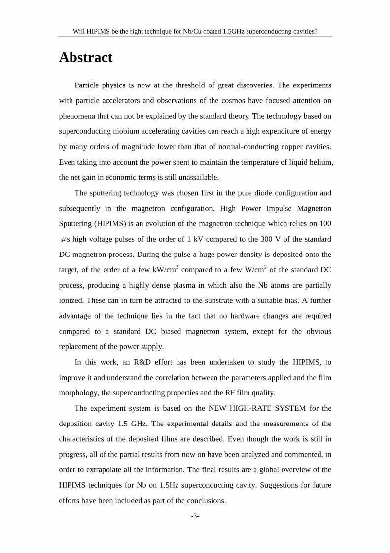
Abstract
Particle physics is now at the threshold of great discoveries. The experiments
with particle accelerators and observations of the cosmos have focused attention on
phenomena that can not be explained by the standard theory. The technology based on
superconducting niobium accelerating cavities can reach a high expenditure of energy
by many orders of magnitude lower than that of normal-conducting copper cavities.
Even taking into account the power spent to maintain the temperature of liquid helium,
the net gain in economic terms is still unassailable.
The sputtering technology was chosen first in the pure diode configuration and
subsequently in the magnetron configuration. High Power Impulse Magnetron
Sputtering (HIPIMS) is an evolution of the magnetron technique which relies on 100
μs high voltage pulses of the order of 1 kV compared to the 300 V of the standard
DC magnetron process. During the pulse a huge power density is deposited onto the
target, of the order of a few kW/cm2 compared to a few W/cm
2 of the standard DC
process, producing a highly dense plasma in which also the Nb atoms are partially
ionized. These can in turn be attracted to the substrate with a suitable bias. A further
advantage of the technique lies in the fact that no hardware changes are required
compared to a standard DC biased magnetron system, except for the obvious
replacement of the power supply.
In this work, an R&D effort has been undertaken to study the HIPIMS, to
improve it and understand the correlation between the parameters applied and the film
morphology, the superconducting properties and the RF film quality.
The experiment system is based on the NEW HIGH-RATE SYSTEM for the
deposition cavity 1.5 GHz. The experimental details and the measurements of the
characteristics of the deposited films are described. Even though the work is still in
progress, all of the partial results from now on have been analyzed and commented, in
order to extrapolate all the information. The final results are a global overview of the
HIPIMS techniques for Nb on 1.5Hz superconducting cavity. Suggestions for future
efforts have been included as part of the conclusions.
Will HIPIMS be the right technique for Nb/Cu coated 1.5GHz superconducting cavities?
-4-
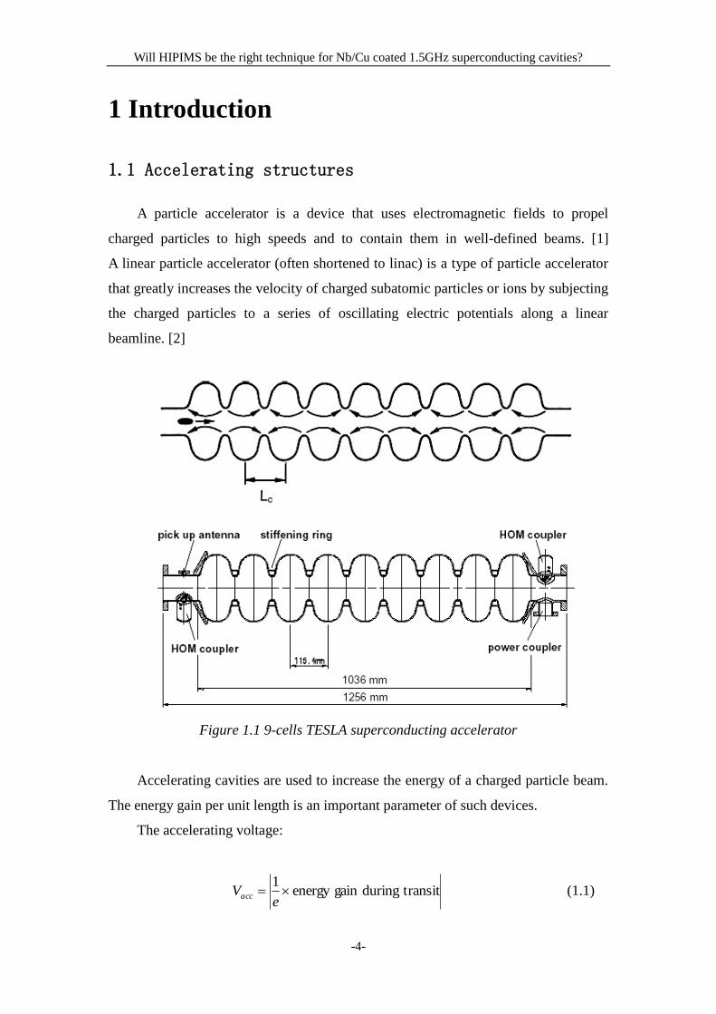
1 Introduction
1.1 Accelerating structures
A particle accelerator is a device that uses electromagnetic fields to propel
charged particles to high speeds and to contain them in well-defined beams. [1]
A linear particle accelerator (often shortened to linac) is a type of particle accelerator
that greatly increases the velocity of charged subatomic particles or ions by subjecting
the charged particles to a series of oscillating electric potentials along a linear
beamline. [2]
Figure 1.1 9-cells TESLA superconducting accelerator
Accelerating cavities are used to increase the energy of a charged particle beam.
The energy gain per unit length is an important parameter of such devices.
The accelerating voltage:
transitduringgain energy 1
eVacc (1.1)
Will HIPIMS be the right technique for Nb/Cu coated 1.5GHz superconducting cavities?
-5-
For particles travelling with the velocity of light c on the symmetry axis in
z–direction and an accelerating mode with eigenfrequency ω this gives:
d
c
zi
zacc dzezEV0
)(
(1.2)
The key parameters of the superconducting accelerating structures are Eacc, Epk
and Hpk.
d
VE a c c
a c c (1.3)
Epk is the highest electric field inside the accelerating structure
Hpk is the highest magnetic field inside the accelerating structure
For a typical TESLA-type cavity, the theoretical maximum accelerating gradient
is about 55 MV/m [3]. At the moment the standard Eacc, achievable in the industrial
production, is about 25-30 MV/m for working TESLA-type accelerating cavities
based on bulk niobium material.
In order to sustain the radiofrequency fields in the cavity, an alternating current
is flowing in the cavity walls. This current dissipates power in the wall as it
experiences a surface resistance.
The power which is dissipated in the cavity:
A
ssA
ssd i s s dAHRdAHRP 22
2
1
2
1 (1.4)
where:
Rs is the global surface resistance
Hs is the magnetic field amplitude
The quality factor Q0:
d i s sP
UQ
0 (1.5)
where:
U is the energy stored in the electromagnetic field in the
Will HIPIMS be the right technique for Nb/Cu coated 1.5GHz superconducting cavities?
-6-
accelerating cavity:
V
dVHU 2
02
1 (1.6)
Also,
sR
GQ 0 (1.7)
where:
G is the geometrical constant; it depends on the geometry of a cavity
and field distribution of the excited mode
A
V
dAH
dVHG
2
2
0 (1.8)
The quality factor can also be defined as:
f
fQ
0 (1.9)
where:
f is the resonance frequency
Δf the full width at half height of the resonance curve in an unloaded
cavity
One can see that the efficiency with which a particle beam can be accelerated in
a radiofrequency cavity depends on the surface resistance. The smaller the resistance
the lower the power dissipated in the cavity walls, the higher the radiofrequency
power available for the particle beam. This is the fundamental advantage of
superconducting cavities as their surface resistance is much lower and outweighs the
power needed to cool the cavities to liquid helium temperatures.
Will HIPIMS be the right technique for Nb/Cu coated 1.5GHz superconducting cavities?
-7-
1.2 Superconducting
Superconductivity is an electrical resistance of exactly zero which occurs in
certain materials below a characteristic temperature. It is also characterized by a
phenomenon called the Meissner effect, the ejection of any sufficiently weak
magnetic field from the interior of the superconductor as it transitions into the
superconducting state. The occurrence of the Meissner effect indicates that
superconductivity cannot be understood simply as the idealization of perfect
conductivity in classical physics. By now a large number of elements and compounds
(mainly alloys and ceramics) have been found showing these behaviors.
Two different types of superconductors were discovered, called respectively type
I and type II. They have certain common features, but differ also in some important
ways. In addition, any external magnetic field up to a critical field B< Bcrit is expelled.
This magnetic field expulsion is called the Meissner-Ochsenfeld effect. This behavior
significantly differs from the properties of an ideal conductor where the field would
be trapped inside the material. Even if the field is switched off, an ideal conductor
would keep the magnetic field and become a permanent magnet as the currents
induced by the field will continue to flow.
Experimentally, Bc can be determined from the area below the magnetization
curve of the material. If the field exceeds a critical value Bc in superconductors of type
I the superconductivity breaks down and the normal conducting state is restored.
This critical field depends on the critical temperature:
2
1)0()(c
ccT
TBTB (1.10)
For the second type of superconductor the magnetic field will start to penetrate
the material above the lower critical field Bc1. Magnetic fluxons enter the material and
their number increases with increasing field. If one raises the field further to a value
of Bc2 the material becomes normalconducting. The temperature dependence of the
critical magnetic fields Bc1 and Bc2 is the same as for the Bc of a type I
Will HIPIMS be the right technique for Nb/Cu coated 1.5GHz superconducting cavities?
-8-
superconductor.
For superconducting cavities niobium shows the most interesting properties. The
general features of superconductivity as well as the special properties of niobium are
described.
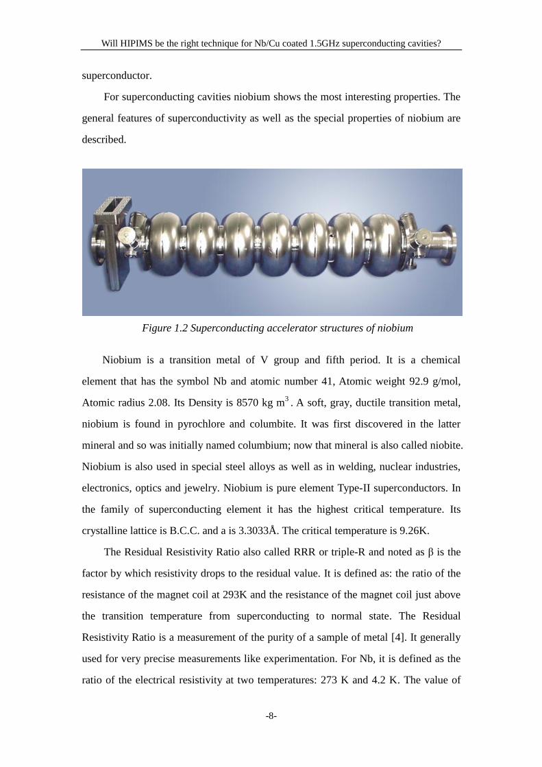
Figure 1.2 Superconducting accelerator structures of niobium
Niobium is a transition metal of V group and fifth period. It is a chemical
element that has the symbol Nb and atomic number 41, Atomic weight 92.9 g/mol,
Atomic radius 2.08. Its Density is 8570 kg m3
. A soft, gray, ductile transition metal,
niobium is found in pyrochlore and columbite. It was first discovered in the latter
mineral and so was initially named columbium; now that mineral is also called niobite.
Niobium is also used in special steel alloys as well as in welding, nuclear industries,
electronics, optics and jewelry. Niobium is pure element Type-II superconductors. In
the family of superconducting element it has the highest critical temperature. Its
crystalline lattice is B.C.C. and a is 3.3033Å. The critical temperature is 9.26K.
The Residual Resistivity Ratio also called RRR or triple-R and noted as β is the
factor by which resistivity drops to the residual value. It is defined as: the ratio of the
resistance of the magnet coil at 293K and the resistance of the magnet coil just above
the transition temperature from superconducting to normal state. The Residual
Resistivity Ratio is a measurement of the purity of a sample of metal [4]. It generally
used for very precise measurements like experimentation. For Nb, it is defined as the
ratio of the electrical resistivity at two temperatures: 273 K and 4.2 K. The value of
Will HIPIMS be the right technique for Nb/Cu coated 1.5GHz superconducting cavities?
-9-
RRR indicates the purity and the low-temperature thermal conductivity of a material,
and is often used as a material specification for superconductors.
For pure Nb used in radio-frequency cavities of linear accelerators, the low
temperature resistivity is defined as the normal-state value extrapolated to 4.2 K, but
this value doesn’t differ much from the 10K value.
)2.4(
)273(
K
KRRR
(1.11)
RRR values serves as a convenient measure of the purity of the metal.
High-purity niobium has higher RRR values; the theoretical limit is 35000 and is
determined by scattering of electrons by lattice vibration.
In a sputtered cavity, the grain size and the purity of the thin film are such that
the mean free path l is very small (10-100 nm) nevertheless the Q0 of such a cavity is
twice that of a cavity made from high RRR bulk niobium.
The mean free path in the niobium is strongly influenced by interstitial impurities
like oxygen, nitrogen and carbon, as well as residual tantalum impurities.
The critical parameter for Superconducting Radio Frequency (SRF) cavities is
the surface resistance Rs, and is where the complex physics comes into play. For
normal-conducting copper cavities operating near room temperature, Rs is simply
determined by the empirically measured bulk electrical conductivity σ by
2
0sR (1.12)
For Type II superconductors in RF fields, Rs can be viewed as the sum of the
superconducting BCS resistance and temperature-independent residual resistances,
resBCSs RRR (1.13)
The BCS resistance derives from BCS theory, which proposed by Bardeen,
Cooper, and Schrieffer. The theory describes superconductivity as a microscopic
effect caused by a condensation of pairs of electrons into a boson-like state [5] [6] [7].
Will HIPIMS be the right technique for Nb/Cu coated 1.5GHz superconducting cavities?
-10-
They assumed that electrons below Tc begin to condense to pairs of electrons, the
so called Cooper pairs. The two electrons in a pair have opposite momentum and spin.
They experience an attractive force mediated via quantized lattice vibrations called
phonons. This bound state of the two electrons is energetically favorable. As the
overall spin of these two paired electrons is zero, many of these pairs can co-exist
coherently, just like other bosons. The coherence length describes the distance over
which the electrons are correlated.
It is given by:
Fhv
(1.14)
where:
vF denotes the velocity of the electrons near the Fermi level
2 is the energy necessary to break up a Cooper pair.
Typical values for the coherence length in niobium are around 39 nm. If one
interprets the coherence length as the size of a Cooper pair, one immediately sees that
it spans over many lattice constants.
Within the BCS theory the energy gap can be calculated:
TkB76.1 (1.15)
One way to view the nature of the BCS RF resistance is that the superconducting
cooper pairs, which have zero resistance for DC current, have finite mass and
momentum which has to alternate sinusoidal for the AC currents of RF fields, thus
giving rise to a small energy loss. The BCS resistance for niobium can be
approximated when the temperature is less than half of niobium's superconducting
critical temperature, T <Tc/2, by:
T
efR
T
BCS
/67.17
9
13 )105.1
(102
(1.16)
Tc=9.3 K for niobium, so that this approximation is valid for T<4.65 K.
Will HIPIMS be the right technique for Nb/Cu coated 1.5GHz superconducting cavities?
-11-
The superconductor's residual resistance arises from several sources, such as
random material defects, hydrides that can form on the surface due to hot chemistry
and slow cool-down, and others that are yet to be identified. One of the quantifiable
residual resistance contributions is due to an external magnetic field pinning magnetic
fluxons in a Type II superconductor. The pinned fluxon cores create small
normal-conducting regions in the niobium that can be summed to estimate their net
resistance.
For niobium, the magnetic field contribution to Rs can be approximated by:
fHRR extHres
121049.9 (1.17)
where:
Hext is any external magnetic field
The residual resistance is usually dominated by lattice imperfections, chemical
impurities, adsorbed gases and trapped magnetic field. Well prepared niobium
surfaces show a residual resistance of a few nΩ
Using the above approximations for a niobium a SRF cavity at 1.8K, 1.3GHz,
and assuming a magnetic field of 10mOe (0.8A/m), the surface resistance components
would be:
RBCS=4.55nΩ
Rres=RH=3.42nΩ
Rs=7.97nΩ.
If for this cavity G=270Ω then the ideal quality factor would be Qo=3.4×10¹⁰
[8]
[9] [10] [11].
Will HIPIMS be the right technique for Nb/Cu coated 1.5GHz superconducting cavities?
-12-
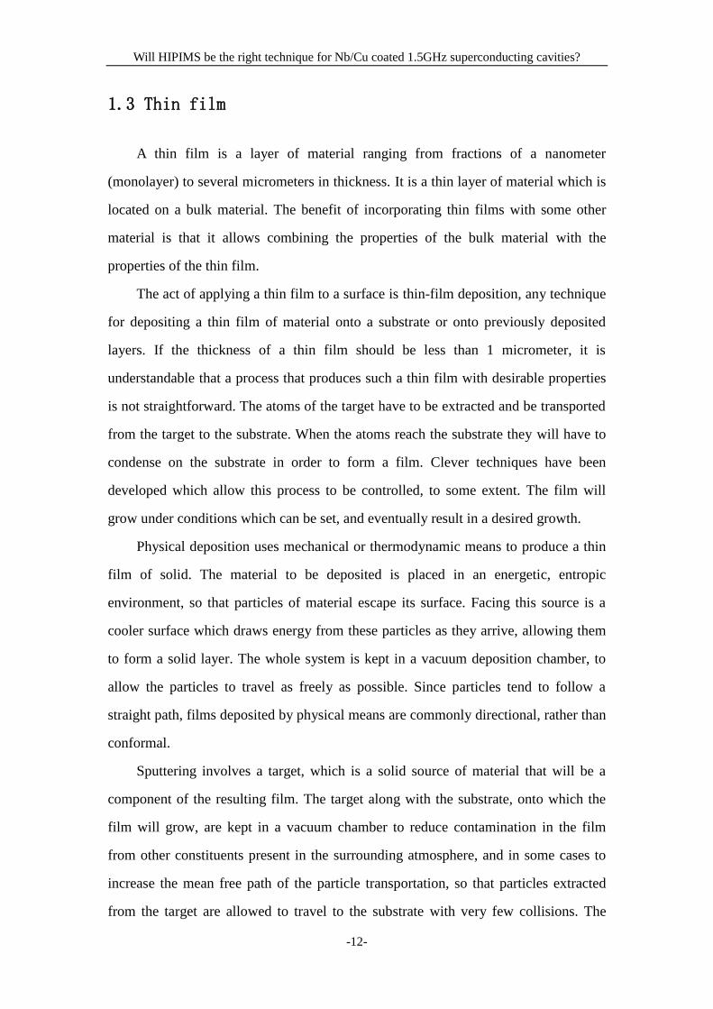
1.3 Thin film
A thin film is a layer of material ranging from fractions of a nanometer
(monolayer) to several micrometers in thickness. It is a thin layer of material which is
located on a bulk material. The benefit of incorporating thin films with some other
material is that it allows combining the properties of the bulk material with the
properties of the thin film.
The act of applying a thin film to a surface is thin-film deposition, any technique
for depositing a thin film of material onto a substrate or onto previously deposited
layers. If the thickness of a thin film should be less than 1 micrometer, it is
understandable that a process that produces such a thin film with desirable properties
is not straightforward. The atoms of the target have to be extracted and be transported
from the target to the substrate. When the atoms reach the substrate they will have to
condense on the substrate in order to form a film. Clever techniques have been
developed which allow this process to be controlled, to some extent. The film will
grow under conditions which can be set, and eventually result in a desired growth.
Physical deposition uses mechanical or thermodynamic means to produce a thin
film of solid. The material to be deposited is placed in an energetic, entropic
environment, so that particles of material escape its surface. Facing this source is a
cooler surface which draws energy from these particles as they arrive, allowing them
to form a solid layer. The whole system is kept in a vacuum deposition chamber, to
allow the particles to travel as freely as possible. Since particles tend to follow a
straight path, films deposited by physical means are commonly directional, rather than
conformal.
Sputtering involves a target, which is a solid source of material that will be a
component of the resulting film. The target along with the substrate, onto which the
film will grow, are kept in a vacuum chamber to reduce contamination in the film
from other constituents present in the surrounding atmosphere, and in some cases to
increase the mean free path of the particle transportation, so that particles extracted
from the target are allowed to travel to the substrate with very few collisions. The
Will HIPIMS be the right technique for Nb/Cu coated 1.5GHz superconducting cavities?
-13-
extraction of particles is a rather complicated process with several steps involved. But
simply explained it can be achieved by applying a negative voltage to the target to
attract positive ions from a working gas inside the chamber. The working gas is
usually argon, which does not react with the film. Thus by using an inert working gas
contamination can be avoided despite the fact that the base pressure usually is high
enough (in the order of 1-100mTorr) to expose the substrate to a significant number of
impinging atoms. In fact, if air would be present instead of argon, a monolayer would
form in about 10-6
s at room temperature. When the ions are attracted onto the target
they will be neutralized and the released energy ideally causes an atom at the surface
of the target to escape in a direction towards the substrate. This is a sputtering event,
and the target atom can now be transported towards the substrate, eventually condense
on the surface and start building a thin film [14].
Will HIPIMS be the right technique for Nb/Cu coated 1.5GHz superconducting cavities?
-14-
2 Magnetron Sputtering
2.1 Fundamentals
Sputtering is a process whereby atoms are ejected from a solid target material
due to bombardment of the target by energetic particles. It is commonly used for
thin-film deposition, etching and analytical techniques [15] [16]. Sputtering
deposition is a physical vapor deposition (PVD) method of depositing thin films.
A material-bombarding particle, like a single atom, ion or molecule with a
relatively high potential energy can give rise to the ejection of secondary electrons or
other phenomenon, like breaking or rearranging chemical bonds. If the kinetic energy
of the bombarding particles exceeds the binding energy of the atoms, atoms of the
lattice are pushed into new position; surface migration of the atoms and surface
damage can arise [17] [18].
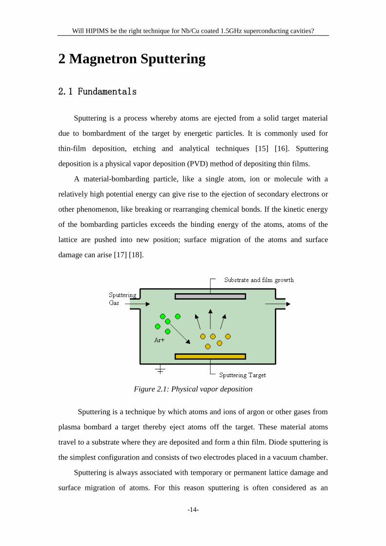
Figure 2.1: Physical vapor deposition
Sputtering is a technique by which atoms and ions of argon or other gases from
plasma bombard a target thereby eject atoms off the target. These material atoms
travel to a substrate where they are deposited and form a thin film. Diode sputtering is
the simplest configuration and consists of two electrodes placed in a vacuum chamber.
Sputtering is always associated with temporary or permanent lattice damage and
surface migration of atoms. For this reason sputtering is often considered as an
Will HIPIMS be the right technique for Nb/Cu coated 1.5GHz superconducting cavities?
-15-
inconvenience as it causes erosion of the electrodes, damage to active surface layers
in thermionic low work-function cathodes, undesirable deposits on walls and
observation windows etc. One can say that sputtering is responsible for limiting the
useful life of a lot of devices including old electronic vacuum triodes (television)
valves or even gas lasers.
If a DC voltage is applied between two electrodes spaced at some distance d
apart in a gas at low pressure, a small current will flow. This is caused by small
number of ions and electrons, which are always present in a gas due ionization, by
cosmic radiation. On their way from the cathode to the anode, the electrons make a
fixed number of ionizing collisions per unit length. Each ionization process produces
further electrons, while resulting ions are accelerated toward the cathode. If the
applied voltage is enough, ions striking the cathode can eject secondary electrons
from its surface. Emission ratio of secondary electrons of most materials is of the
order of 0.1, so several ions are needed to bombard a given area of the cathode in
order to release secondary electrons. If the power supplied is not high enough, the
bombardment is concentrated near the edges of the cathode. When the power supplied
increases, the bombardment covers the entire cathode surface and a constant current is
achieved.
The two processes of ionization by electron impact and secondary emission of
electrons by ions, control the current I in the system, described by the equation
)1(1
0
d
d
e
eII
(2.1)
where:
I0 is the primary electron current generated at the cathode by the external
source
αis the number of ions per unit length produced by the electrons
d is the spacing between the electrodes
γ is the number of secondary electrons emitted per incident ion.
Will HIPIMS be the right technique for Nb/Cu coated 1.5GHz superconducting cavities?
-16-
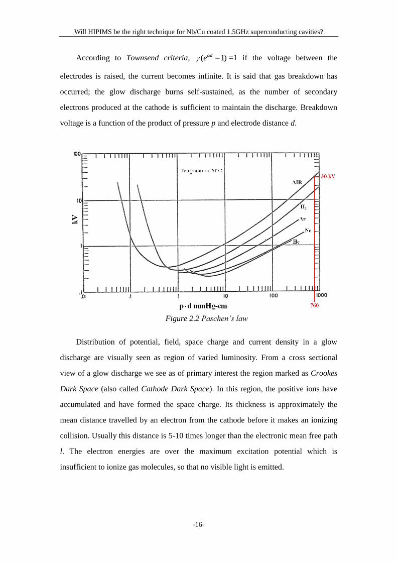
According to Townsend criteria, )1( de =1 if the voltage between the
electrodes is raised, the current becomes infinite. It is said that gas breakdown has
occurred; the glow discharge burns self-sustained, as the number of secondary
electrons produced at the cathode is sufficient to maintain the discharge. Breakdown
voltage is a function of the product of pressure p and electrode distance d.
Figure 2.2 Paschen’s law
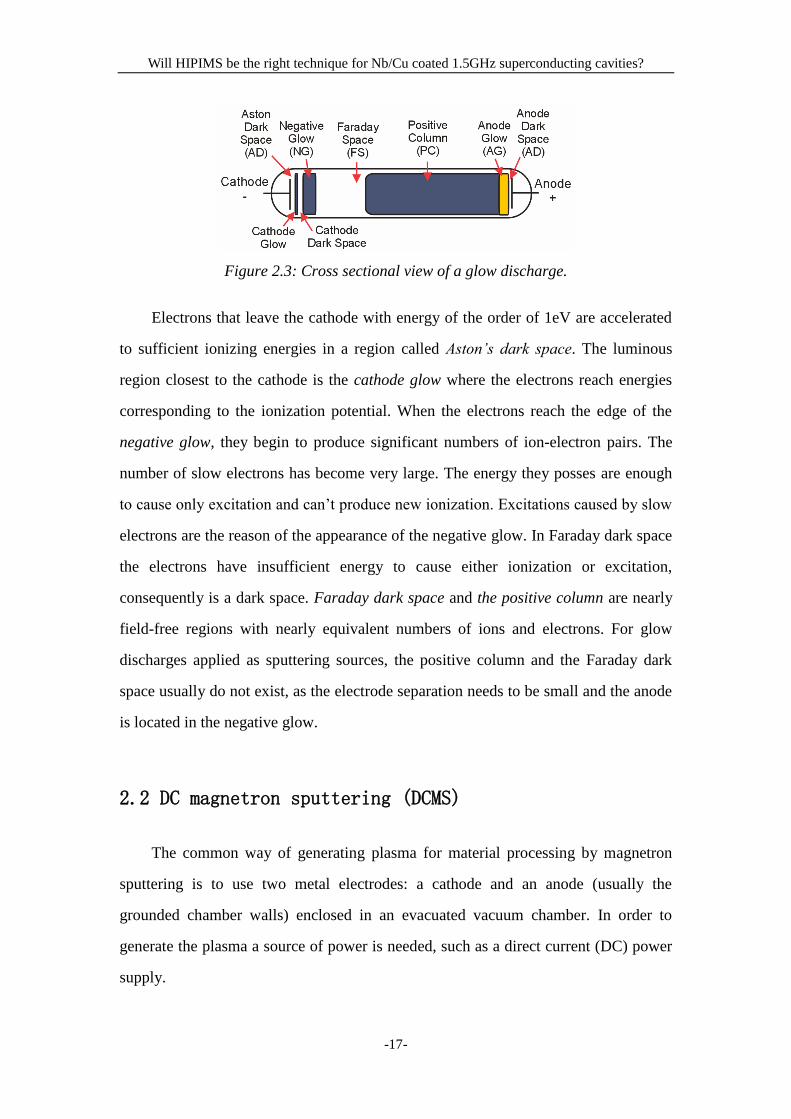
Distribution of potential, field, space charge and current density in a glow
discharge are visually seen as region of varied luminosity. From a cross sectional
view of a glow discharge we see as of primary interest the region marked as Crookes
Dark Space (also called Cathode Dark Space). In this region, the positive ions have
accumulated and have formed the space charge. Its thickness is approximately the
mean distance travelled by an electron from the cathode before it makes an ionizing
collision. Usually this distance is 5-10 times longer than the electronic mean free path
l. The electron energies are over the maximum excitation potential which is
insufficient to ionize gas molecules, so that no visible light is emitted.
Will HIPIMS be the right technique for Nb/Cu coated 1.5GHz superconducting cavities?
-17-
Figure 2.3: Cross sectional view of a glow discharge.
Electrons that leave the cathode with energy of the order of 1eV are accelerated
to sufficient ionizing energies in a region called Aston’s dark space. The luminous
region closest to the cathode is the cathode glow where the electrons reach energies
corresponding to the ionization potential. When the electrons reach the edge of the
negative glow, they begin to produce significant numbers of ion-electron pairs. The
number of slow electrons has become very large. The energy they posses are enough
to cause only excitation and can’t produce new ionization. Excitations caused by slow
electrons are the reason of the appearance of the negative glow. In Faraday dark space
the electrons have insufficient energy to cause either ionization or excitation,
consequently is a dark space. Faraday dark space and the positive column are nearly
field-free regions with nearly equivalent numbers of ions and electrons. For glow
discharges applied as sputtering sources, the positive column and the Faraday dark
space usually do not exist, as the electrode separation needs to be small and the anode
is located in the negative glow.
2.2 DC magnetron sputtering (DCMS)
The common way of generating plasma for material processing by magnetron
sputtering is to use two metal electrodes: a cathode and an anode (usually the
grounded chamber walls) enclosed in an evacuated vacuum chamber. In order to
generate the plasma a source of power is needed, such as a direct current (DC) power
supply.
Will HIPIMS be the right technique for Nb/Cu coated 1.5GHz superconducting cavities?
-18-
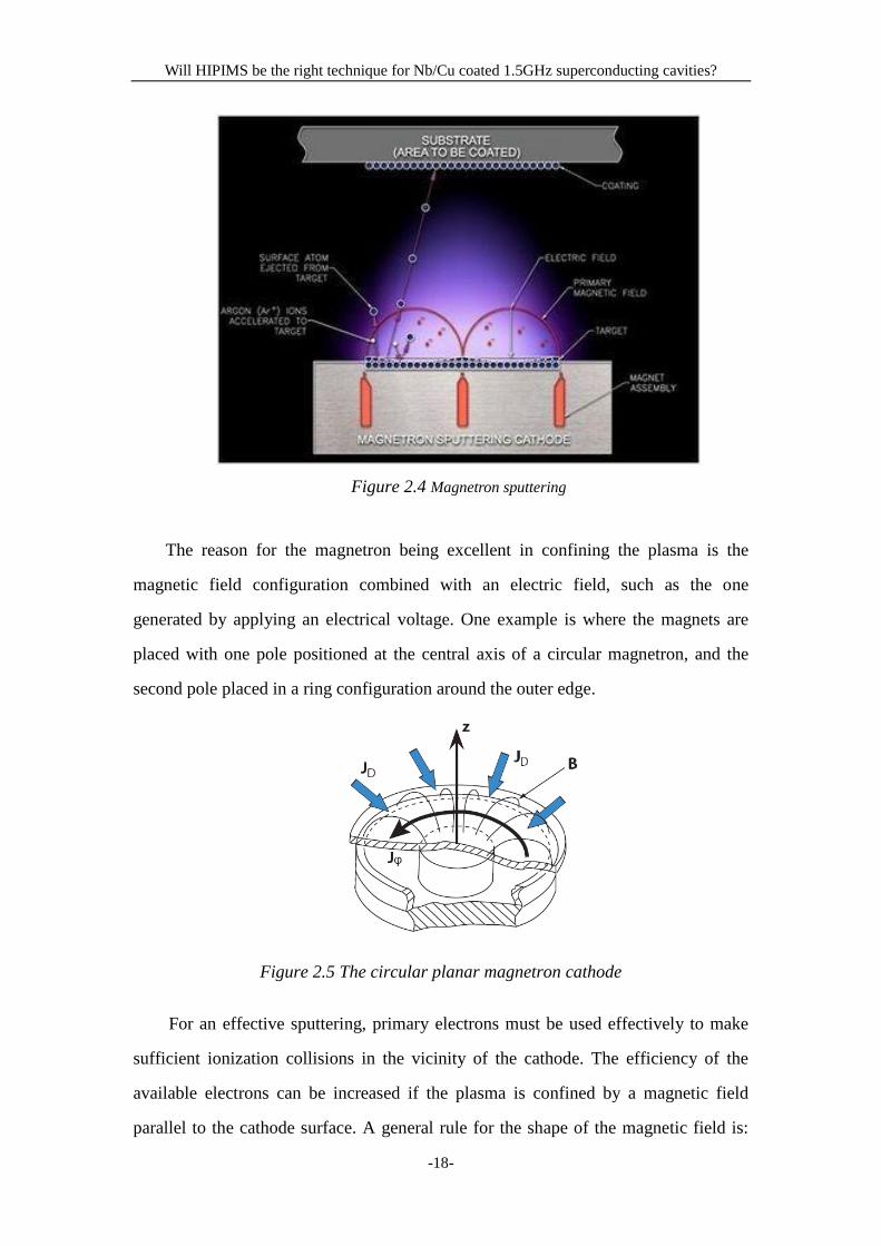
Figure 2.4 Magnetron sputtering
The reason for the magnetron being excellent in confining the plasma is the
magnetic field configuration combined with an electric field, such as the one
generated by applying an electrical voltage. One example is where the magnets are
placed with one pole positioned at the central axis of a circular magnetron, and the
second pole placed in a ring configuration around the outer edge.
Figure 2.5 The circular planar magnetron cathode
For an effective sputtering, primary electrons must be used effectively to make
sufficient ionization collisions in the vicinity of the cathode. The efficiency of the
available electrons can be increased if the plasma is confined by a magnetic field
parallel to the cathode surface. A general rule for the shape of the magnetic field is:
Will HIPIMS be the right technique for Nb/Cu coated 1.5GHz superconducting cavities?
-19-
Magnetic field must bore from the cathode and die onto the target. That means that a
plasma confinement is achieved, while magnetic and/or electrostatic mirrors trap the
electrons. The magnetic field traps and forces electrons to describe helical paths
around the lines of magnetic force.
The magnets are arranged in such a way that they create a closed drift region;
electrons are trapped, and rely on collisions to escape. By trapping the electrons in
this way, the probability for ionization is increased by orders of magnitudes. Ions are
also subjected to the same force, but due to their larger mass, the Larmor radius often
exceeds the dimensions of the plasma.
Larmor radius:
B
W
B
V
e
mVr Ee
c
Eg 37.3)(
(2.2)
where:
VE is the drift speed of electrons
W is the energy associated with the electron motion perpendicular to
the field
Although in general one says that the ions are not directly confined, they are so
indirectly by trapping the electrons, to keep the quasi neutrality of the plasma. The
trapping of electrons and ions creates dense plasma, which in turn leads to an
increased ion bombardment of the target, giving higher sputtering rates and, therefore,
higher deposition rates at the substrate. The electron confinement also allows for a
magnetron to be operated at much lower voltages compared to basic sputtering (~ 500
V instead of 2-3 kV) and be used at lower pressures (typically mTorr region). This is
an advantage since less material is lost to the chamber wall and back to the target
through scattering in the discharge gas. The shape of the magnetic field efficiently
erodes the target where the magnetic field lines are parallel to the target surface; a
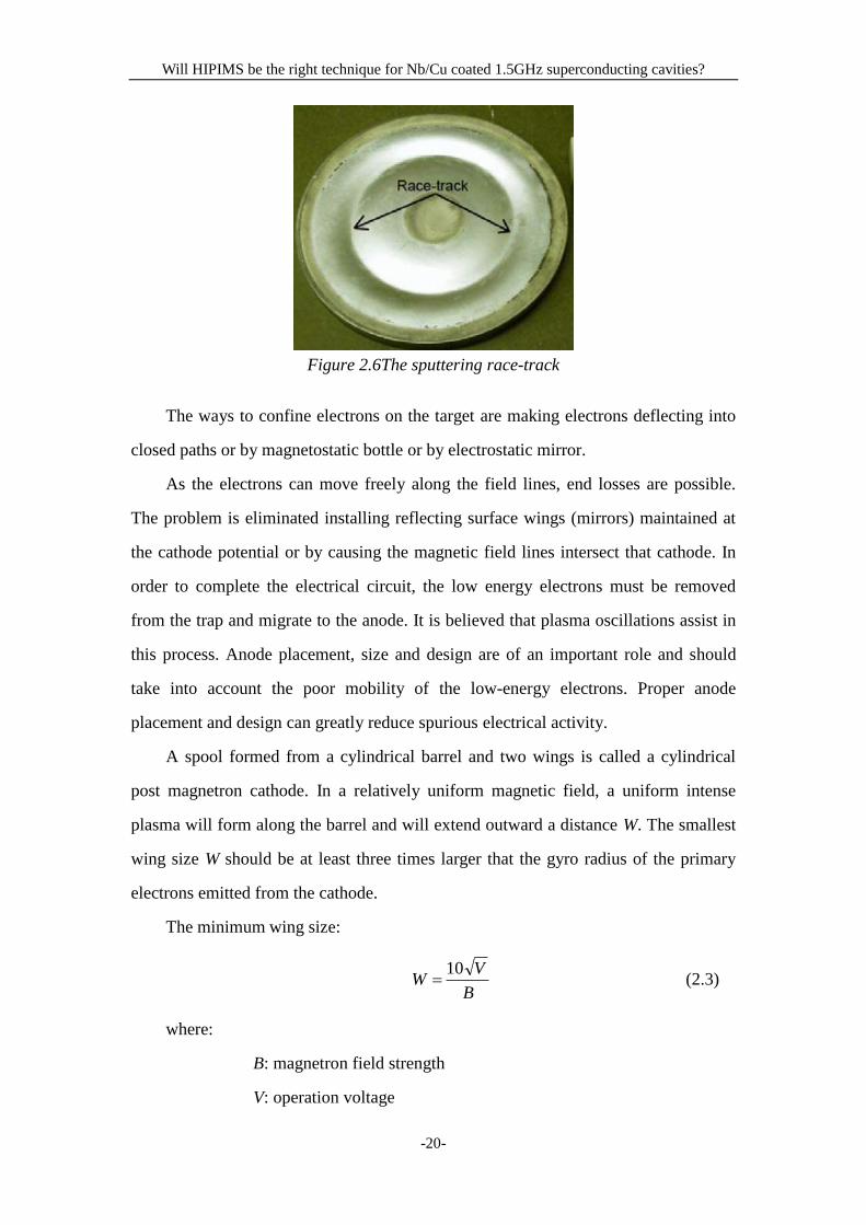
so-called race-track is created.
Will HIPIMS be the right technique for Nb/Cu coated 1.5GHz superconducting cavities?
-20-
Figure 2.6The sputtering race-track
The ways to confine electrons on the target are making electrons deflecting into
closed paths or by magnetostatic bottle or by electrostatic mirror.
As the electrons can move freely along the field lines, end losses are possible.
The problem is eliminated installing reflecting surface wings (mirrors) maintained at
the cathode potential or by causing the magnetic field lines intersect that cathode. In
order to complete the electrical circuit, the low energy electrons must be removed
from the trap and migrate to the anode. It is believed that plasma oscillations assist in
this process. Anode placement, size and design are of an important role and should
take into account the poor mobility of the low-energy electrons. Proper anode
placement and design can greatly reduce spurious electrical activity.
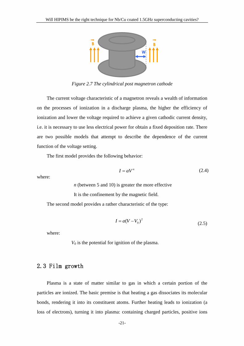
A spool formed from a cylindrical barrel and two wings is called a cylindrical
post magnetron cathode. In a relatively uniform magnetic field, a uniform intense
plasma will form along the barrel and will extend outward a distance W. The smallest
wing size W should be at least three times larger that the gyro radius of the primary
electrons emitted from the cathode.
The minimum wing size:
B
VW
10 (2.3)
where:
B: magnetron field strength
V: operation voltage
Will HIPIMS be the right technique for Nb/Cu coated 1.5GHz superconducting cavities?
-21-
Figure 2.7 The cylindrical post magnetron cathode
The current voltage characteristic of a magnetron reveals a wealth of information
on the processes of ionization in a discharge plasma, the higher the efficiency of
ionization and lower the voltage required to achieve a given cathodic current density,
i.e. it is necessary to use less electrical power for obtain a fixed deposition rate. There
are two possible models that attempt to describe the dependence of the current
function of the voltage setting.
The first model provides the following behavior:
(2.4)
where:
n (between 5 and 10) is greater the more effective
It is the confinement by the magnetic field.
The second model provides a rather characteristic of the type:
2
0 )( VVaI (2.5)
where:
V0 is the potential for ignition of the plasma.
2.3 Film growth
Plasma is a state of matter similar to gas in which a certain portion of the
particles are ionized. The basic premise is that heating a gas dissociates its molecular
bonds, rendering it into its constituent atoms. Further heating leads to ionization (a
loss of electrons), turning it into plasma: containing charged particles, positive ions
B
W
B
B
naVI
Will HIPIMS be the right technique for Nb/Cu coated 1.5GHz superconducting cavities?
-22-
and negative electrons [19].
Plasmas are used in a number of ways in the field of thin film production and
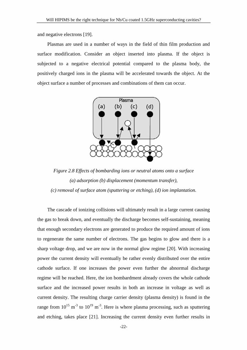
surface modification. Consider an object inserted into plasma. If the object is
subjected to a negative electrical potential compared to the plasma body, the
positively charged ions in the plasma will be accelerated towards the object. At the
object surface a number of processes and combinations of them can occur.
Figure 2.8 Effects of bombarding ions or neutral atoms onto a surface
(a) adsorption (b) displacement (momentum transfer),
(c) removal of surface atom (sputtering or etching), (d) ion implantation.
The cascade of ionizing collisions will ultimately result in a large current causing
the gas to break down, and eventually the discharge becomes self-sustaining, meaning
that enough secondary electrons are generated to produce the required amount of ions
to regenerate the same number of electrons. The gas begins to glow and there is a
sharp voltage drop, and we are now in the normal glow regime [20]. With increasing
power the current density will eventually be rather evenly distributed over the entire
cathode surface. If one increases the power even further the abnormal discharge
regime will be reached. Here, the ion bombardment already covers the whole cathode
surface and the increased power results in both an increase in voltage as well as
current density. The resulting charge carrier density (plasma density) is found in the
range from 1015
m-3
to 1019
m-3
. Here is where plasma processing, such as sputtering
and etching, takes place [21]. Increasing the current density even further results in
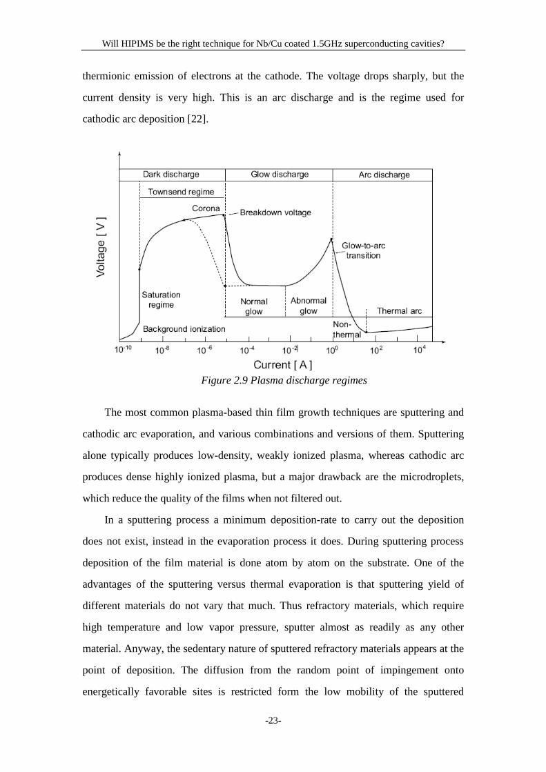
Will HIPIMS be the right technique for Nb/Cu coated 1.5GHz superconducting cavities?
-23-
thermionic emission of electrons at the cathode. The voltage drops sharply, but the
current density is very high. This is an arc discharge and is the regime used for
cathodic arc deposition [22].
Figure 2.9 Plasma discharge regimes
The most common plasma-based thin film growth techniques are sputtering and
cathodic arc evaporation, and various combinations and versions of them. Sputtering
alone typically produces low-density, weakly ionized plasma, whereas cathodic arc
produces dense highly ionized plasma, but a major drawback are the microdroplets,
which reduce the quality of the films when not filtered out.
In a sputtering process a minimum deposition-rate to carry out the deposition
does not exist, instead in the evaporation process it does. During sputtering process
deposition of the film material is done atom by atom on the substrate. One of the
advantages of the sputtering versus thermal evaporation is that sputtering yield of
different materials do not vary that much. Thus refractory materials, which require
high temperature and low vapor pressure, sputter almost as readily as any other
material. Anyway, the sedentary nature of sputtered refractory materials appears at the
point of deposition. The diffusion from the random point of impingement onto
energetically favorable sites is restricted form the low mobility of the sputtered
Will HIPIMS be the right technique for Nb/Cu coated 1.5GHz superconducting cavities?
-24-
material. The microstructure and properties of coating deposited is, however,
influenced a lot from the plasma sputtering environment, which can be manipulated
[23]. Without any modification of the plasma environment one can obtain primitive
growth structures that are not strongly interbonded.
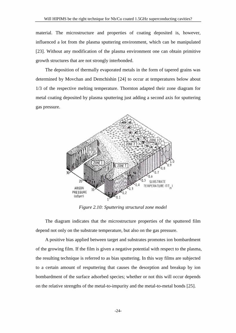
The deposition of thermally evaporated metals in the form of tapered grains was
determined by Movchan and Demchishin [24] to occur at temperatures below about
1/3 of the respective melting temperature. Thornton adapted their zone diagram for
metal coating deposited by plasma sputtering just adding a second axis for sputtering
gas pressure.
Figure 2.10: Sputtering structural zone model
The diagram indicates that the microstructure properties of the sputtered film
depend not only on the substrate temperature, but also on the gas pressure.
A positive bias applied between target and substrates promotes ion bombardment
of the growing film. If the film is given a negative potential with respect to the plasma,
the resulting technique is referred to as bias sputtering. In this way films are subjected
to a certain amount of resputtering that causes the desorption and breakup by ion
bombardment of the surface adsorbed species; whether or not this will occur depends
on the relative strengths of the metal-to-impurity and the metal-to-metal bonds [25].
Will HIPIMS be the right technique for Nb/Cu coated 1.5GHz superconducting cavities?
-25-
The impurity fraction:
RN
Nf
ii
iii
(2.4)
where:
Ni is the number of atoms of species i bombarding unit area of film in
unit time during deposition
αi is the effective sticking coefficient of the species i during deposition
R is the deposition rate of the film
Considering the bias:
RN
Nf
ii
iii
(2.5)
where:
β is a function of the bias current due to impurities ions
From early morphology studies, the film structure is highly correlated with the
deposition rate and the adatom surface mobility [26, 27]. By increasing the incident
atom energy and incident flux, we can expect increased substrate temperature right at
the surface, and higher adatom surface mobility, which leads to the larger grain size.
Based on this and the findings in [28], Schucan et. al., have tried to use Ar/He mixture
as working gas to increase the argon ionization efficiency during sputtering [29].
Unfortunately rare gas trapping reduces the grain size and affects the grain growth.
The investigation of the rare gas trapping of Ar, Ke and Xe is reported in [30].
Sputtering film technique has the following drawbacks:
· the working gas is trapped in the film; it may cause intrinsic defects inside of
the grain. And the impurities of the working gas are not good for the thin film.
· the deposition energy is low, which does not help to avoid columnar grains.
Will HIPIMS be the right technique for Nb/Cu coated 1.5GHz superconducting cavities?
-26-
3 HIPIMS
3.1 Fundamental
High Power Impulse Magnetron Sputtering (HIPIMS), also known as High
Power Pulsed Magnetron Sputtering (HPPMS) is a method for physical vapor
deposition of thin films which is based on magnetron sputter deposition. HIPIMS
utilizes extremely high power densities of the order of kWcm−2
in short pulses
(impulses) of tens of microseconds at low duty cycle (on/off time ratio) of < 10%. A
distinguishing feature of HIPIMS is its high degree of ionization of the sputtered
metal and high rate of molecular gas dissociation.
HIPIMS was first reported in 1999 by Kouznetsov et al, [31-37] who also
patented the technique together with the company Chemfilt R&D. The basis of the
technique is to increase the plasma density in front of a sputtering source, and, thereby,
decreasing the mean ionization distance for the sputtered particles. The increase in
plasma density is simply achieved by applying a high electrical power. The electrical
power applied to the target surface has to be high enough so electron densities of the
order of 1019
–1020
m-3
are reached in the vicinity of the sputtering source. In reality
this corresponds to electrical power of the order of kWcm-2
on the target surface,
which is too much to be run in constant mode with conventional target cooling. The
solution to this problem is to apply the high power in pulses with a low duty factor.
The duty factor is the ratio of the pulse on time and the cycle time. The target cooling
is limited by the average power rather than the peak power, and by applying the
power in pulses the average power can be kept at where the cooling is sufficient. The
discharge is uniformly distributed over the target surface. This is necessary to avoid
the formation of microdroplets.
The peak power that must be delivered to the target is typically of the order of
kWcm-2
, meaning that the power supply must be able to deliver a peak electrical
power in the range 10kW-5MW, depending on the target size. The pulse is then
repeated with such a frequency that the average power is kept low.
Will HIPIMS be the right technique for Nb/Cu coated 1.5GHz superconducting cavities?
-27-
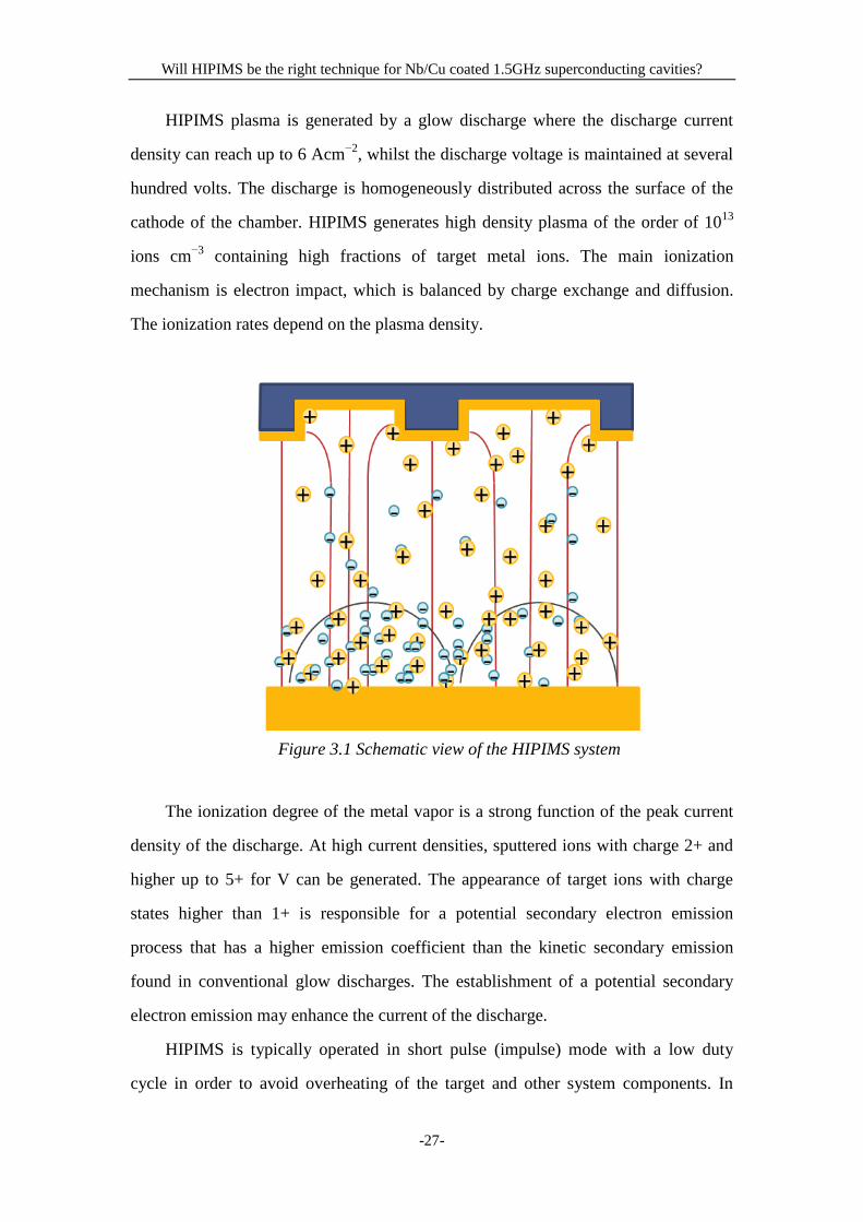
HIPIMS plasma is generated by a glow discharge where the discharge current
density can reach up to 6 Acm−2
, whilst the discharge voltage is maintained at several
hundred volts. The discharge is homogeneously distributed across the surface of the
cathode of the chamber. HIPIMS generates high density plasma of the order of 1013
ions cm−3
containing high fractions of target metal ions. The main ionization
mechanism is electron impact, which is balanced by charge exchange and diffusion.
The ionization rates depend on the plasma density.
Figure 3.1 Schematic view of the HIPIMS system
The ionization degree of the metal vapor is a strong function of the peak current
density of the discharge. At high current densities, sputtered ions with charge 2+ and
higher up to 5+ for V can be generated. The appearance of target ions with charge
states higher than 1+ is responsible for a potential secondary electron emission
process that has a higher emission coefficient than the kinetic secondary emission
found in conventional glow discharges. The establishment of a potential secondary
electron emission may enhance the current of the discharge.
HIPIMS is typically operated in short pulse (impulse) mode with a low duty
cycle in order to avoid overheating of the target and other system components. In
Will HIPIMS be the right technique for Nb/Cu coated 1.5GHz superconducting cavities?
-28-
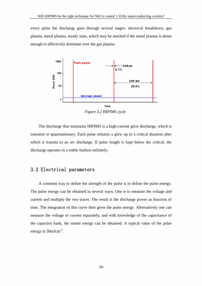
every pulse the discharge goes through several stages: electrical breakdown, gas
plasma, metal plasma, steady state, which may be reached if the metal plasma is dense
enough to effectively dominate over the gas plasma
Figure 3.2 HIPIMS cycle
The discharge that maintains HIPIMS is a high-current glow discharge, which is
transient or quasistationary. Each pulse remains a glow up to a critical duration after
which it transits to an arc discharge. If pulse length is kept below the critical, the
discharge operates in a stable fashion infinitely.
3.2 Electrical parameters
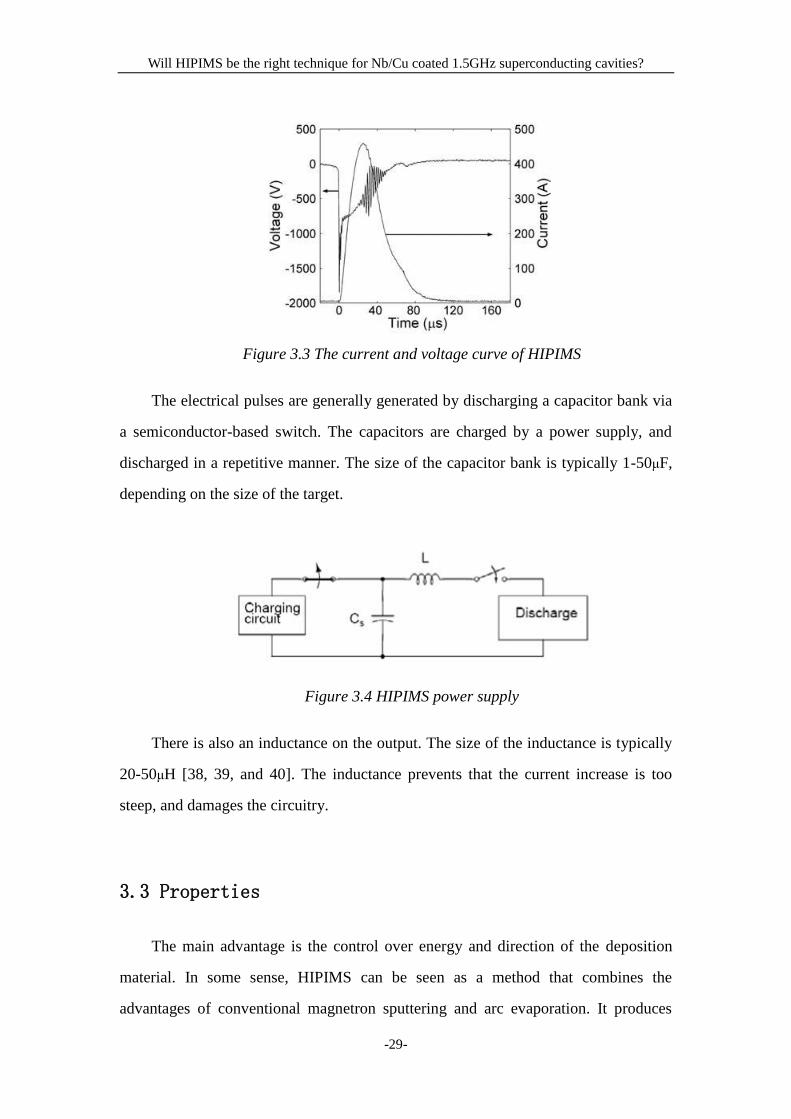
A common way to define the strength of the pulse is to define the pulse energy.
The pulse energy can be obtained in several ways. One is to measure the voltage and
current and multiply the two traces. The result is the discharge power as function of
time. The integration of this curve then gives the pulse energy. Alternatively one can
measure the voltage or current separately, and with knowledge of the capacitance of
the capacitor bank, the stored energy can be obtained. A typical value of the pulse
energy is 50mJcm-2
.
Will HIPIMS be the right technique for Nb/Cu coated 1.5GHz superconducting cavities?
-29-
Figure 3.3 The current and voltage curve of HIPIMS
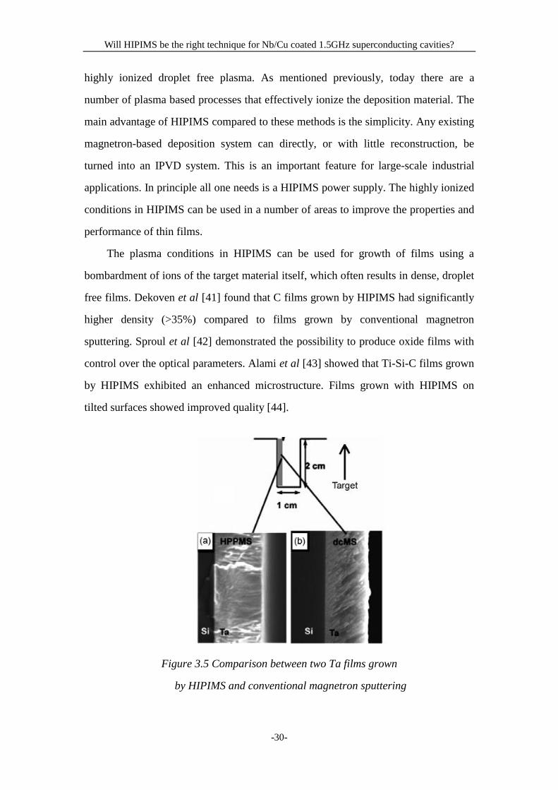
The electrical pulses are generally generated by discharging a capacitor bank via
a semiconductor-based switch. The capacitors are charged by a power supply, and
discharged in a repetitive manner. The size of the capacitor bank is typically 1-50μF,
depending on the size of the target.
Figure 3.4 HIPIMS power supply
There is also an inductance on the output. The size of the inductance is typically
20-50μH [38, 39, and 40]. The inductance prevents that the current increase is too
steep, and damages the circuitry.
3.3 Properties
The main advantage is the control over energy and direction of the deposition
material. In some sense, HIPIMS can be seen as a method that combines the
advantages of conventional magnetron sputtering and arc evaporation. It produces
Will HIPIMS be the right technique for Nb/Cu coated 1.5GHz superconducting cavities?
-30-
highly ionized droplet free plasma. As mentioned previously, today there are a
number of plasma based processes that effectively ionize the deposition material. The
main advantage of HIPIMS compared to these methods is the simplicity. Any existing
magnetron-based deposition system can directly, or with little reconstruction, be
turned into an IPVD system. This is an important feature for large-scale industrial
applications. In principle all one needs is a HIPIMS power supply. The highly ionized
conditions in HIPIMS can be used in a number of areas to improve the properties and
performance of thin films.
The plasma conditions in HIPIMS can be used for growth of films using a
bombardment of ions of the target material itself, which often results in dense, droplet
free films. Dekoven et al [41] found that C films grown by HIPIMS had significantly
higher density (>35%) compared to films grown by conventional magnetron
sputtering. Sproul et al [42] demonstrated the possibility to produce oxide films with
control over the optical parameters. Alami et al [43] showed that Ti-Si-C films grown
by HIPIMS exhibited an enhanced microstructure. Films grown with HIPIMS on
tilted surfaces showed improved quality [44].
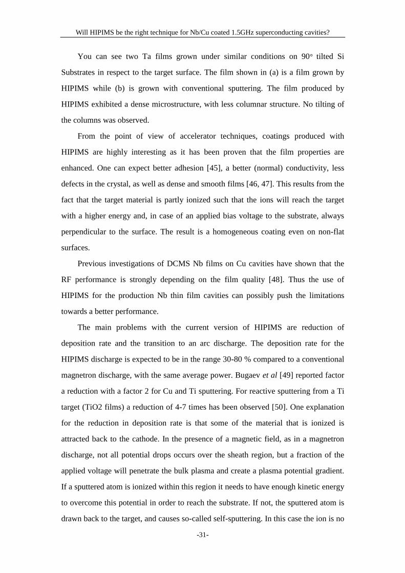
Figure 3.5 Comparison between two Ta films grown
by HIPIMS and conventional magnetron sputtering
Will HIPIMS be the right technique for Nb/Cu coated 1.5GHz superconducting cavities?
-31-
You can see two Ta films grown under similar conditions on 90° tilted Si
Substrates in respect to the target surface. The film shown in (a) is a film grown by
HIPIMS while (b) is grown with conventional sputtering. The film produced by
HIPIMS exhibited a dense microstructure, with less columnar structure. No tilting of
the columns was observed.
From the point of view of accelerator techniques, coatings produced with
HIPIMS are highly interesting as it has been proven that the film properties are
enhanced. One can expect better adhesion [45], a better (normal) conductivity, less
defects in the crystal, as well as dense and smooth films [46, 47]. This results from the
fact that the target material is partly ionized such that the ions will reach the target
with a higher energy and, in case of an applied bias voltage to the substrate, always
perpendicular to the surface. The result is a homogeneous coating even on non-flat
surfaces.
Previous investigations of DCMS Nb films on Cu cavities have shown that the
RF performance is strongly depending on the film quality [48]. Thus the use of
HIPIMS for the production Nb thin film cavities can possibly push the limitations
towards a better performance.
The main problems with the current version of HIPIMS are reduction of
deposition rate and the transition to an arc discharge. The deposition rate for the
HIPIMS discharge is expected to be in the range 30-80 % compared to a conventional
magnetron discharge, with the same average power. Bugaev et al [49] reported factor
a reduction with a factor 2 for Cu and Ti sputtering. For reactive sputtering from a Ti
target (TiO2 films) a reduction of 4-7 times has been observed [50]. One explanation
for the reduction in deposition rate is that some of the material that is ionized is
attracted back to the cathode. In the presence of a magnetic field, as in a magnetron
discharge, not all potential drops occurs over the sheath region, but a fraction of the
applied voltage will penetrate the bulk plasma and create a plasma potential gradient.
If a sputtered atom is ionized within this region it needs to have enough kinetic energy
to overcome this potential in order to reach the substrate. If not, the sputtered atom is
drawn back to the target, and causes so-called self-sputtering. In this case the ion is no
Will HIPIMS be the right technique for Nb/Cu coated 1.5GHz superconducting cavities?
-32-
longer available for deposition, and the rate drops. A plot of the deposition rate for
HIPIMS compared to conventional sputtering versus the ratio between the
self-sputtering yield, and the Ar yield (that is the dominant mechanism in
conventional sputtering) is evidence that self-sputtering is an important mechanism in
HIPIMS.
The other problem with HIPIMS is the arcing tendency on the cathode surface.
There are mainly two types of arcs. Heavy arcs and light arcs. The light arc is minor
problem, since it does not produce large number of microdroplets, as the heavy arc
does. The light arc can be seen as a little spark on the target surface that does not
extend further into the bulk plasma. The heavy arc can however be a serious problem.
Heavy arcs can sometimes be observed as extended plasma columns going from the
cathode into the bulk plasma. The arc locally heats the target, and microdroplets can
be ejected.
3.4 Applications
HIPIMS is currently taking the first steps towards industrial applications. The
unique features of the discharge should be well suited for a number of application
areas.
One of them is surface pre-treatment. The highly ionized and metallic plasma is
well suited for combined etching and ion implantation. These might involve adhesion
enhancer for coatings on various tools (etching) and adhesion layer for coatings on
various substrates
Another is film growth. The current version of HIPIMS, with the reduced
deposition rate, should be applied to products where the increase in production cost is
small in comparison to the gain in film quality. These can be areas where really thin
films are desired or for coatings on expensive products, for example high-tech
electronics.
Will HIPIMS be the right technique for Nb/Cu coated 1.5GHz superconducting cavities?
-33-
A few suggested application areas are:
1) Metallization in general
2) Interconnects in IC structures
3) Protective overcoats on hard disks and read-write heads
4) Deposition onto complex shaped objects
5) Coatings on medical products
6) Conducting & transparent electrodes in flat panel displays touch panel
displays, solar cells, etc.
7) Al coatings in numerous applications
8) Optical coatings: anti-reflective and anti-static coatings, optical filters
9) Wear-corrosion-resistive coatings: cutting tools, tribological applications, etc.
10) Ag mirrors
11) Coatings on plastics
Will HIPIMS be the right technique for Nb/Cu coated 1.5GHz superconducting cavities?
-34-
4 Experiment system
4.1 Introduction
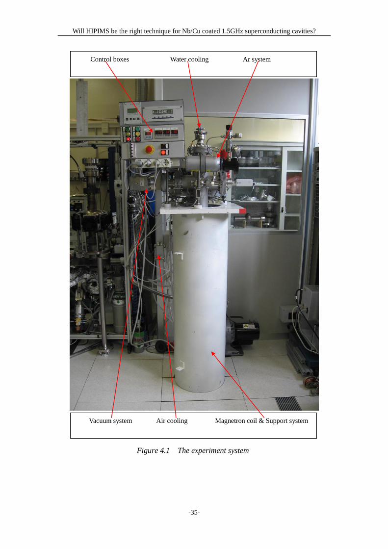
The experiment system is consisted of the following parts:
1 The vacuum system. High to ultra-high vacuum removes the obstruction of air,
allowing particle beams to deposit.
2 The control system. Including control box and baking box, manages and
commands the behavior of the experiment system.
3 The cooling system. Including water cooling and air cooling, transfers the
thermal energy out of the experiment system.
4 The Ar supply system. Argon is preferred for the sputter coating; it is the
cheapest noble gases, since it is a byproduct of the production of liquid oxygen and
liquid nitrogen from a cryogenic air separation unit, both of which are used on a large
industrial scale. Also, argon is the most plentiful since it has the highest concentration
in the atmosphere. The bulk of argon applications arise simply because it is inert and
relatively cheap.
5 The magnetron coil and support system. The magnetron coil is used to produce
the external magnetic field, for not limiting the Curie temperature permanent magnets
and to simplify the structure of the maximum post magnetron and minimize the
problems related to high temperatures that have occurred during the preliminary tests.
Also, all the system is standing upon the coil.
Will HIPIMS be the right technique for Nb/Cu coated 1.5GHz superconducting cavities?
-35-
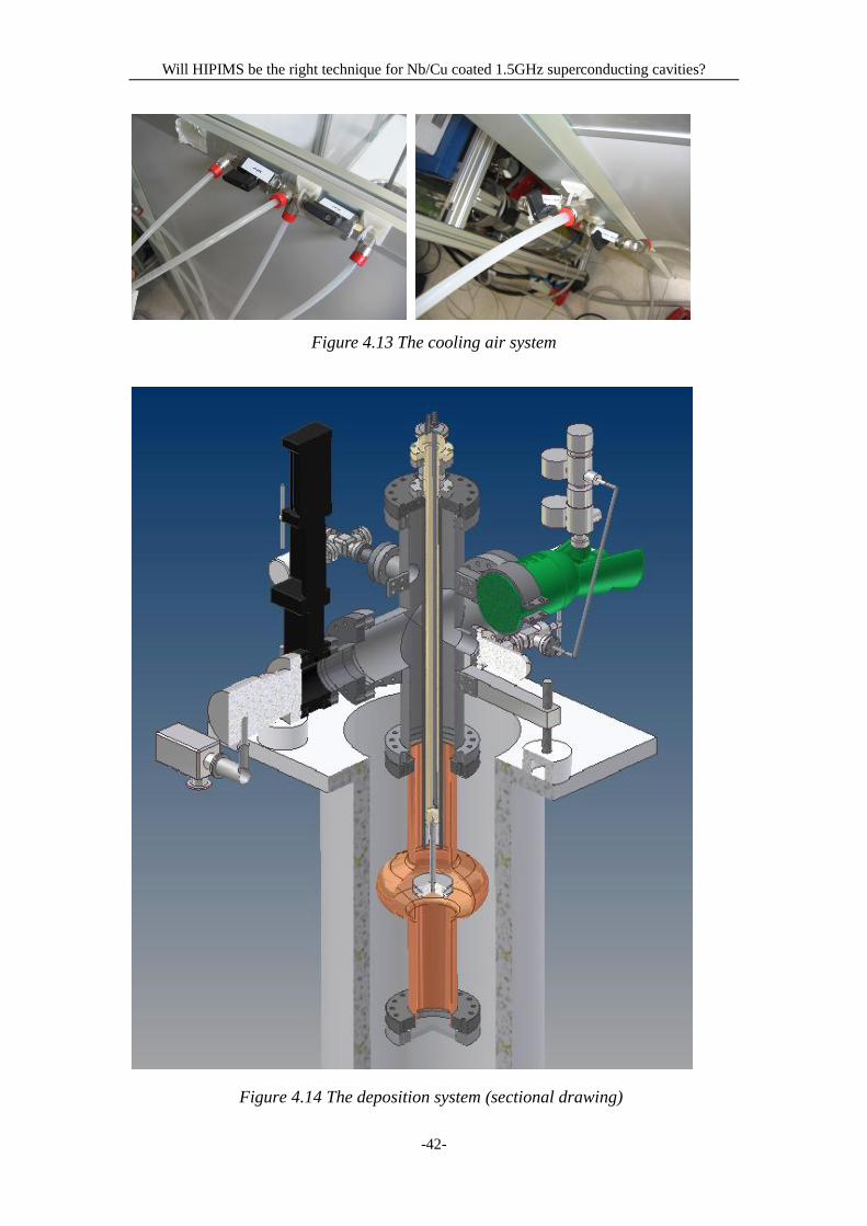
Figure 4.1 The experiment system
Control boxes Water cooling Ar system
Vacuum system Air cooling Magnetron coil & Support system
Will HIPIMS be the right technique for Nb/Cu coated 1.5GHz superconducting cavities?
-36-
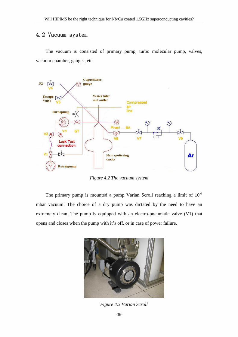
4.2 Vacuum system
The vacuum is consisted of primary pump, turbo molecular pump, valves,
vacuum chamber, gauges, etc.
Figure 4.2 The vacuum system
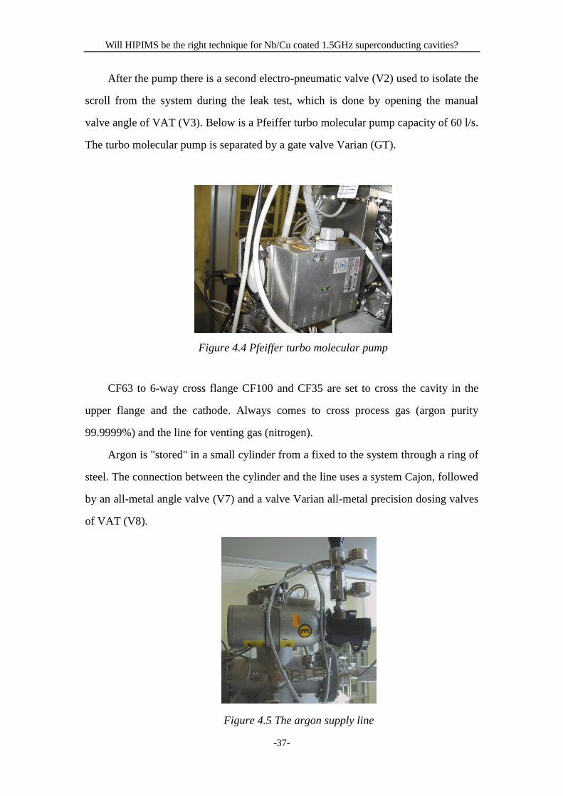
The primary pump is mounted a pump Varian Scroll reaching a limit of 10-2
mbar vacuum. The choice of a dry pump was dictated by the need to have an
extremely clean. The pump is equipped with an electro-pneumatic valve (V1) that
opens and closes when the pump with it’s off, or in case of power failure.
Figure 4.3 Varian Scroll
Will HIPIMS be the right technique for Nb/Cu coated 1.5GHz superconducting cavities?
-37-
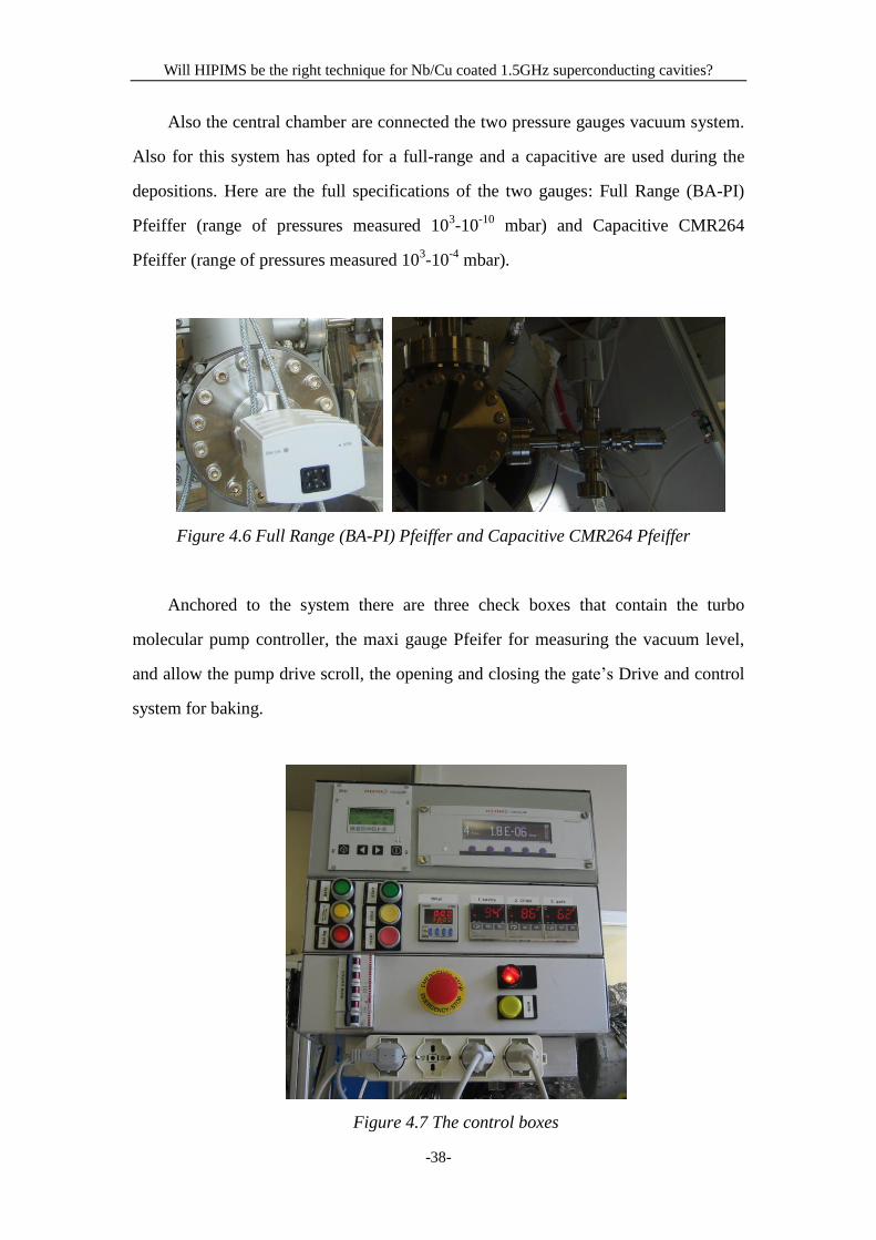
After the pump there is a second electro-pneumatic valve (V2) used to isolate the
scroll from the system during the leak test, which is done by opening the manual
valve angle of VAT (V3). Below is a Pfeiffer turbo molecular pump capacity of 60 l/s.
The turbo molecular pump is separated by a gate valve Varian (GT).
Figure 4.4 Pfeiffer turbo molecular pump
CF63 to 6-way cross flange CF100 and CF35 are set to cross the cavity in the
upper flange and the cathode. Always comes to cross process gas (argon purity
99.9999%) and the line for venting gas (nitrogen).
Argon is "stored" in a small cylinder from a fixed to the system through a ring of
steel. The connection between the cylinder and the line uses a system Cajon, followed
by an all-metal angle valve (V7) and a valve Varian all-metal precision dosing valves
of VAT (V8).
Figure 4.5 The argon supply line
Will HIPIMS be the right technique for Nb/Cu coated 1.5GHz superconducting cavities?
-38-
Also the central chamber are connected the two pressure gauges vacuum system.
Also for this system has opted for a full-range and a capacitive are used during the
depositions. Here are the full specifications of the two gauges: Full Range (BA-PI)
Pfeiffer (range of pressures measured 103-10
-10 mbar) and Capacitive CMR264
Pfeiffer (range of pressures measured 103-10
-4 mbar).
Figure 4.6 Full Range (BA-PI) Pfeiffer and Capacitive CMR264 Pfeiffer
Anchored to the system there are three check boxes that contain the turbo
molecular pump controller, the maxi gauge Pfeifer for measuring the vacuum level,
and allow the pump drive scroll, the opening and closing the gate’s Drive and control
system for baking.
Figure 4.7 The control boxes
Will HIPIMS be the right technique for Nb/Cu coated 1.5GHz superconducting cavities?
-39-
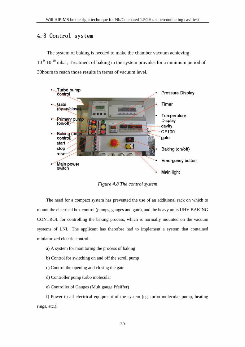
4.3 Control system
The system of baking is needed to make the chamber vacuum achieving
10-9
-10-10
mbar, Treatment of baking in the system provides for a minimum period of
30hours to reach those results in terms of vacuum level.
Figure 4.8 The control system
The need for a compact system has prevented the use of an additional rack on which to
mount the electrical box control (pumps, gauges and gate), and the heavy units UHV BAKING
CONTROL for controlling the baking process, which is normally mounted on the vacuum
systems of LNL. The applicant has therefore had to implement a system that contained
miniaturized electric control:
a) A system for monitoring the process of baking
b) Control for switching on and off the scroll pump
c) Control the opening and closing the gate
d) Controller pump turbo molecular
e) Controller of Gauges (Multigauge Pfeiffer)
f) Power to all electrical equipment of the system (eg, turbo molecular pump, heating
rings, etc.).
Will HIPIMS be the right technique for Nb/Cu coated 1.5GHz superconducting cavities?
-40-
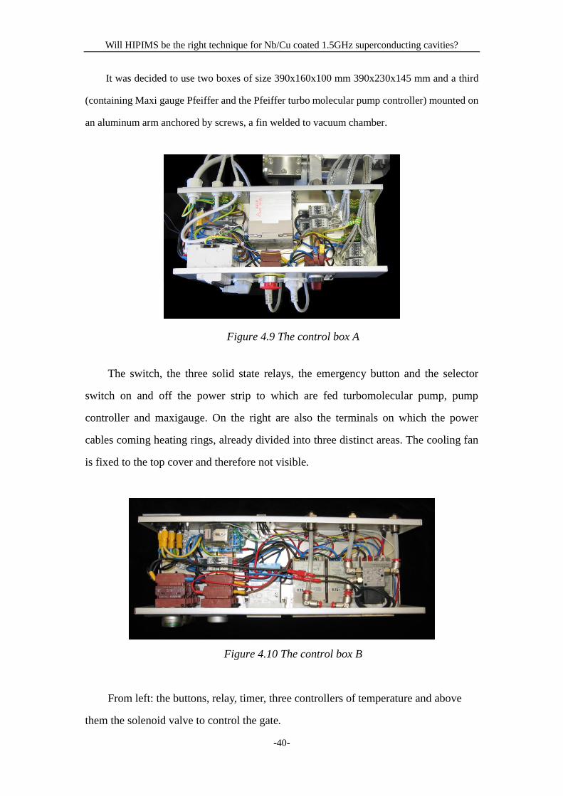
It was decided to use two boxes of size 390x160x100 mm 390x230x145 mm and a third
(containing Maxi gauge Pfeiffer and the Pfeiffer turbo molecular pump controller) mounted on
an aluminum arm anchored by screws, a fin welded to vacuum chamber.
Figure 4.9 The control box A
The switch, the three solid state relays, the emergency button and the selector
switch on and off the power strip to which are fed turbomolecular pump, pump
controller and maxigauge. On the right are also the terminals on which the power
cables coming heating rings, already divided into three distinct areas. The cooling fan
is fixed to the top cover and therefore not visible.
Figure 4.10 The control box B
From left: the buttons, relay, timer, three controllers of temperature and above
them the solenoid valve to control the gate.
Will HIPIMS be the right technique for Nb/Cu coated 1.5GHz superconducting cavities?
-41-
4.4 The cathode
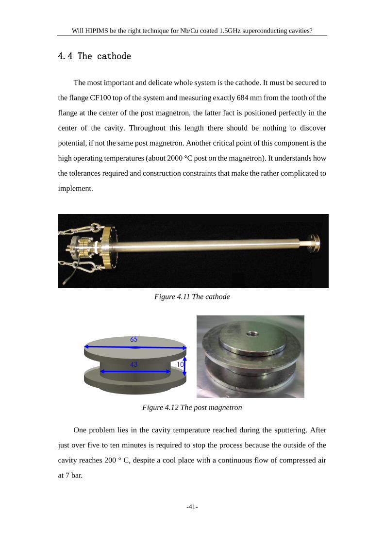
The most important and delicate whole system is the cathode. It must be secured to
the flange CF100 top of the system and measuring exactly 684 mm from the tooth of the
flange at the center of the post magnetron, the latter fact is positioned perfectly in the
center of the cavity. Throughout this length there should be nothing to discover
potential, if not the same post magnetron. Another critical point of this component is the
high operating temperatures (about 2000 °C post on the magnetron). It understands how
the tolerances required and construction constraints that make the rather complicated to
implement.
Figure 4.11 The cathode
Figure 4.12 The post magnetron
One problem lies in the cavity temperature reached during the sputtering. After
just over five to ten minutes is required to stop the process because the outside of the
cavity reaches 200 ° C, despite a cool place with a continuous flow of compressed air
at 7 bar.
43
65
10
Will HIPIMS be the right technique for Nb/Cu coated 1.5GHz superconducting cavities?
-42-
Figure 4.13 The cooling air system
Figure 4.14 The deposition system (sectional drawing)
Will HIPIMS be the right technique for Nb/Cu coated 1.5GHz superconducting cavities?
-43-
4.5 The power supply
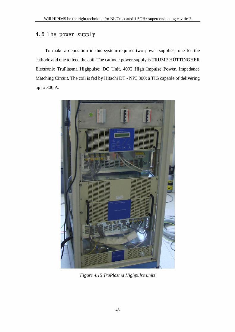
To make a deposition in this system requires two power supplies, one for the
cathode and one to feed the coil. The cathode power supply is TRUMF HÜTTINGHER
Electronic TruPlasma Highpulse: DC Unit, 4002 High Impulse Power, Impedance
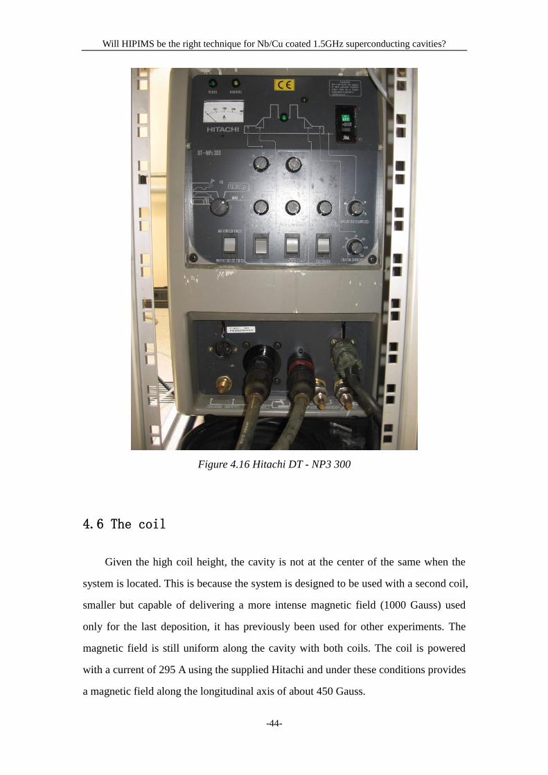
Matching Circuit. The coil is fed by Hitachi DT - NP3 300; a TIG capable of delivering
up to 300 A.
Figure 4.15 TruPlasma Highpulse units
Will HIPIMS be the right technique for Nb/Cu coated 1.5GHz superconducting cavities?
-44-
Figure 4.16 Hitachi DT - NP3 300
4.6 The coil
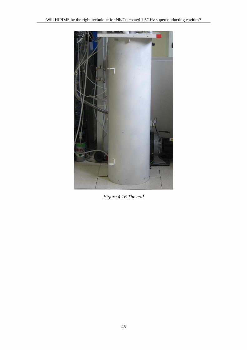
Given the high coil height, the cavity is not at the center of the same when the
system is located. This is because the system is designed to be used with a second coil,
smaller but capable of delivering a more intense magnetic field (1000 Gauss) used
only for the last deposition, it has previously been used for other experiments. The
magnetic field is still uniform along the cavity with both coils. The coil is powered
with a current of 295 A using the supplied Hitachi and under these conditions provides
a magnetic field along the longitudinal axis of about 450 Gauss.
Will HIPIMS be the right technique for Nb/Cu coated 1.5GHz superconducting cavities?
-45-
Figure 4.16 The coil
Will HIPIMS be the right technique for Nb/Cu coated 1.5GHz superconducting cavities?
-46-
5 Experimental details
5.1 Ultrasonic Cleaning
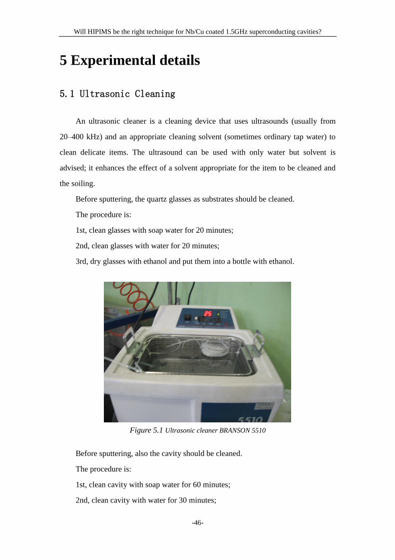
An ultrasonic cleaner is a cleaning device that uses ultrasounds (usually from
20–400 kHz) and an appropriate cleaning solvent (sometimes ordinary tap water) to
clean delicate items. The ultrasound can be used with only water but solvent is
advised; it enhances the effect of a solvent appropriate for the item to be cleaned and
the soiling.
Before sputtering, the quartz glasses as substrates should be cleaned.
The procedure is:
1st, clean glasses with soap water for 20 minutes;
2nd, clean glasses with water for 20 minutes;
3rd, dry glasses with ethanol and put them into a bottle with ethanol.
Figure 5.1 Ultrasonic cleaner BRANSON 5510
Before sputtering, also the cavity should be cleaned.
The procedure is:
1st, clean cavity with soap water for 60 minutes;
2nd, clean cavity with water for 30 minutes;
Will HIPIMS be the right technique for Nb/Cu coated 1.5GHz superconducting cavities?
-47-
3rd, dry cavity with ethanol and air, and then cover them with aluminum.
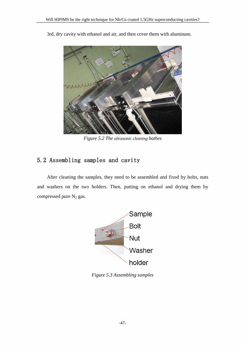
Figure 5.2 The ultrasonic cleaning bathes
5.2 Assembling samples and cavity
After cleaning the samples, they need to be assembled and fixed by bolts, nuts
and washers on the two holders. Then, putting on ethanol and drying them by
compressed pure N2 gas.
Figure 5.3 Assembling samples
Will HIPIMS be the right technique for Nb/Cu coated 1.5GHz superconducting cavities?
-48-
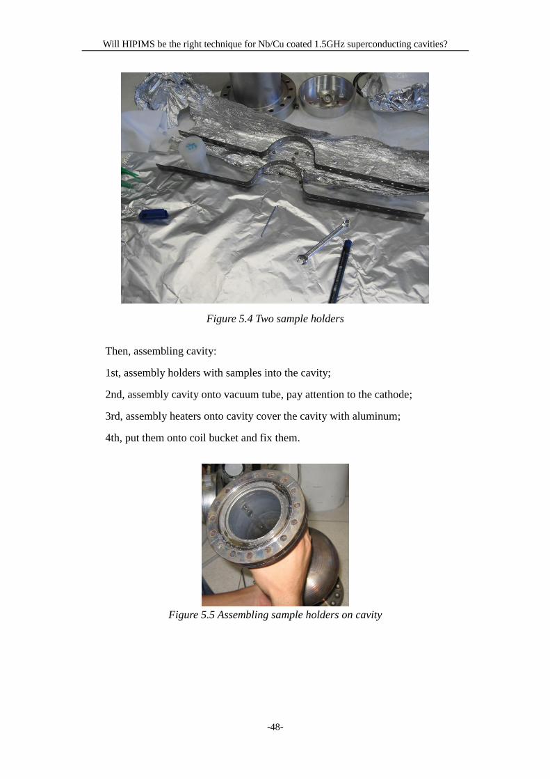
Figure 5.4 Two sample holders
Then, assembling cavity:
1st, assembly holders with samples into the cavity;
2nd, assembly cavity onto vacuum tube, pay attention to the cathode;
3rd, assembly heaters onto cavity cover the cavity with aluminum;
4th, put them onto coil bucket and fix them.
Figure 5.5 Assembling sample holders on cavity
Will HIPIMS be the right technique for Nb/Cu coated 1.5GHz superconducting cavities?
-49-
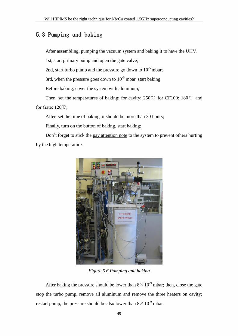
5.3 Pumping and baking
After assembling, pumping the vacuum system and baking it to have the UHV.
1st, start primary pump and open the gate valve;
2nd, start turbo pump and the pressure go down to 10-5
mbar;
3rd, when the pressure goes down to 10-6
mbar, start baking.
Before baking, cover the system with aluminum;
Then, set the temperatures of baking: for cavity: 250℃ for CF100: 180℃ and
for Gate: 120℃;
After, set the time of baking, it should be more than 30 hours;
Finally, turn on the button of baking, start baking;
Don’t forget to stick the pay attention note to the system to prevent others hurting
by the high temperature.
Figure 5.6 Pumping and baking
After baking the pressure should be lower than 8×10⁻⁹
mbar; then, close the gate,
stop the turbo pump, remove all aluminum and remove the three heaters on cavity;
restart pump, the pressure should be also lower than 8×10⁻⁹
mbar.
Will HIPIMS be the right technique for Nb/Cu coated 1.5GHz superconducting cavities?
-50-
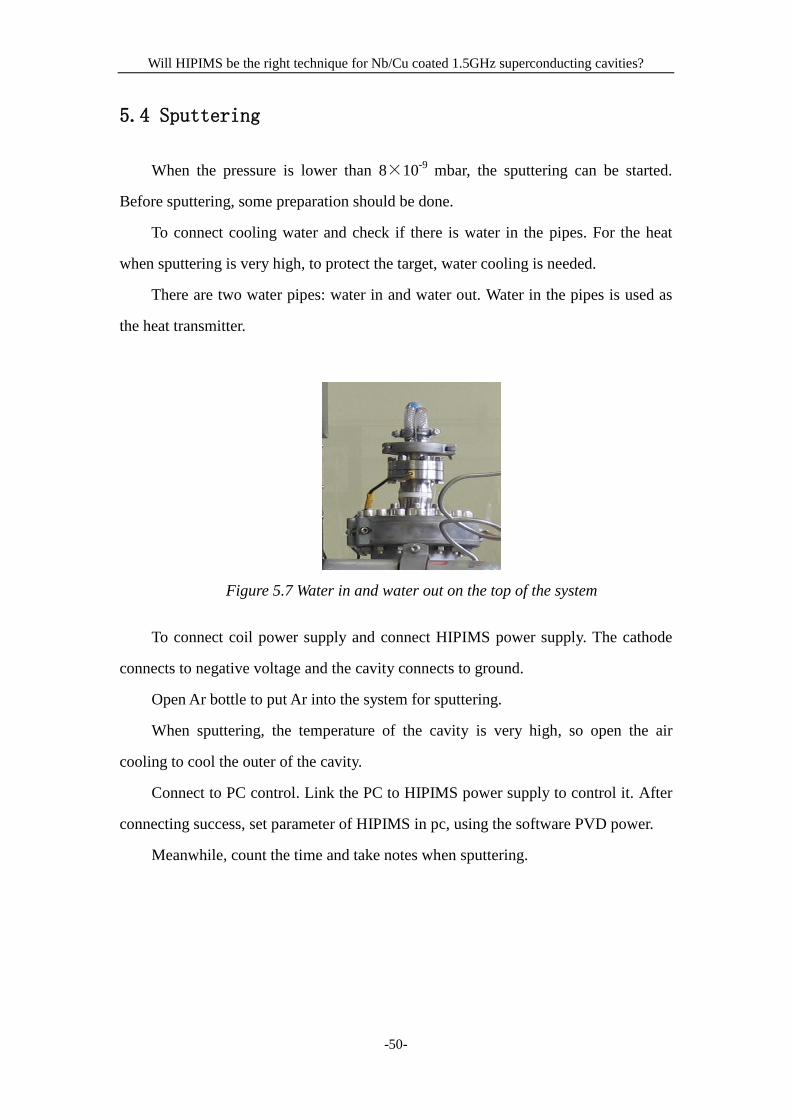
5.4 Sputtering
When the pressure is lower than 8×10⁻⁹
mbar, the sputtering can be started.
Before sputtering, some preparation should be done.
To connect cooling water and check if there is water in the pipes. For the heat
when sputtering is very high, to protect the target, water cooling is needed.
There are two water pipes: water in and water out. Water in the pipes is used as
the heat transmitter.
Figure 5.7 Water in and water out on the top of the system
To connect coil power supply and connect HIPIMS power supply. The cathode
connects to negative voltage and the cavity connects to ground.
Open Ar bottle to put Ar into the system for sputtering.
When sputtering, the temperature of the cavity is very high, so open the air
cooling to cool the outer of the cavity.
Connect to PC control. Link the PC to HIPIMS power supply to control it. After
connecting success, set parameter of HIPIMS in pc, using the software PVD power.
Meanwhile, count the time and take notes when sputtering.
Will HIPIMS be the right technique for Nb/Cu coated 1.5GHz superconducting cavities?
-51-
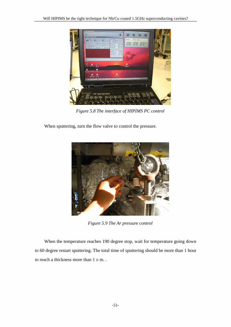
Figure 5.8 The interface of HIPIMS PC control
When sputtering, turn the flow valve to control the pressure.
Figure 5.9 The Ar pressure control
When the temperature reaches 190 degree stop, wait for temperature going down
to 60 degree restart sputtering. The total time of sputtering should be more than 1 hour
to reach a thickness more than 1μm. .
Will HIPIMS be the right technique for Nb/Cu coated 1.5GHz superconducting cavities?
-52-
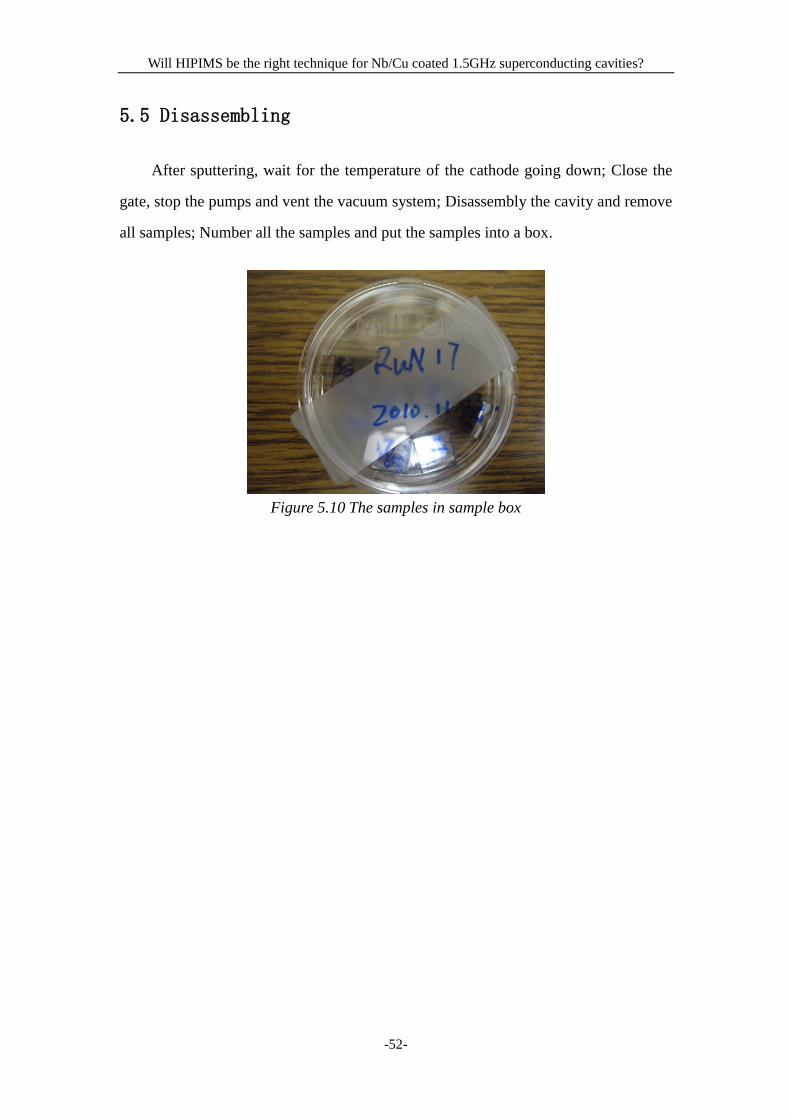
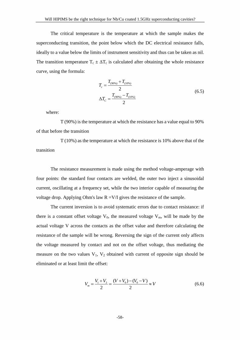
5.5 Disassembling
After sputtering, wait for the temperature of the cathode going down; Close the
gate, stop the pumps and vent the vacuum system; Disassembly the cavity and remove
all samples; Number all the samples and put the samples into a box.
Figure 5.10 The samples in sample box
Will HIPIMS be the right technique for Nb/Cu coated 1.5GHz superconducting cavities?
-53-
6 The characterization techniques
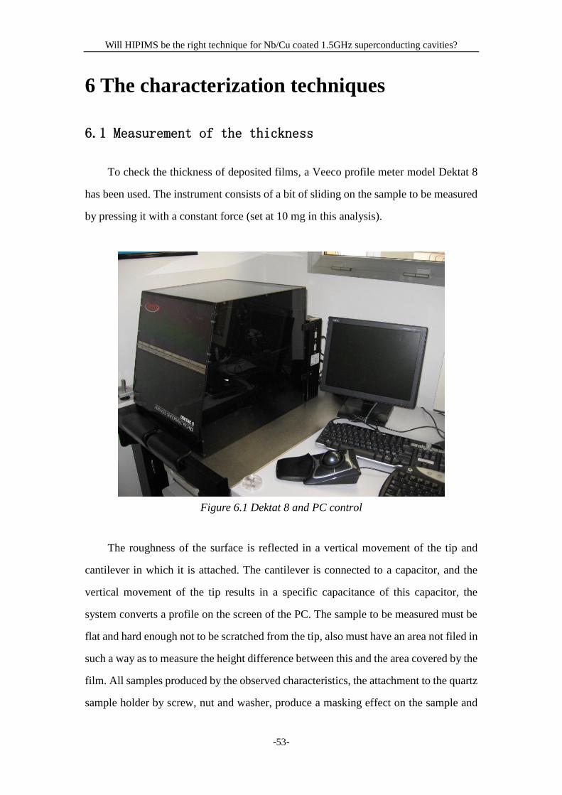
6.1 Measurement of the thickness
To check the thickness of deposited films, a Veeco profile meter model Dektat 8
has been used. The instrument consists of a bit of sliding on the sample to be measured
by pressing it with a constant force (set at 10 mg in this analysis).
Figure 6.1 Dektat 8 and PC control
The roughness of the surface is reflected in a vertical movement of the tip and
cantilever in which it is attached. The cantilever is connected to a capacitor, and the
vertical movement of the tip results in a specific capacitance of this capacitor, the
system converts a profile on the screen of the PC. The sample to be measured must be
flat and hard enough not to be scratched from the tip, also must have an area not filed in
such a way as to measure the height difference between this and the area covered by the
film. All samples produced by the observed characteristics, the attachment to the quartz
sample holder by screw, nut and washer, produce a masking effect on the sample and
Will HIPIMS be the right technique for Nb/Cu coated 1.5GHz superconducting cavities?
-54-
thus allow the analysis to the profile meter. The scan is performed from the area that
had not been filed with the movie, to prevent an error in the selection of scan length, to
bring out the tip from the sample, causing serious damage.
The Scan parameters are:
Scan Type: Standard Scan
Stylus: Radius 5μm
Length: 2500μm
Duration: 20sec
Force: 10mg
Measurement Range: 65500nm
Profile: Hills & Valleys
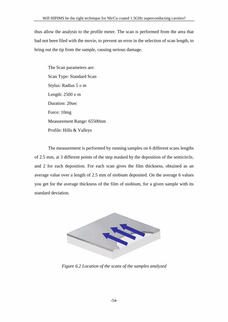
The measurement is performed by running samples on 6 different scans lengths
of 2.5 mm, at 3 different points of the step masked by the deposition of the semicircle,
and 2 for each deposition. For each scan gives the film thickness, obtained as an
average value over a length of 2.5 mm of niobium deposited. On the average 6 values
you get for the average thickness of the film of niobium, for a given sample with its
standard deviation.
Figure 6.2 Location of the scans of the samples analyzed
Will HIPIMS be the right technique for Nb/Cu coated 1.5GHz superconducting cavities?
-55-
6.2 Measurement of the reticular parameters
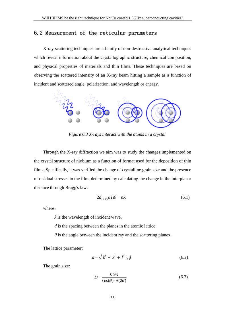
X-ray scattering techniques are a family of non-destructive analytical techniques
which reveal information about the crystallographic structure, chemical composition,
and physical properties of materials and thin films. These techniques are based on
observing the scattered intensity of an X-ray beam hitting a sample as a function of
incident and scattered angle, polarization, and wavelength or energy.
Figure 6.3 X-rays interact with the atoms in a crystal
Through the X-ray diffraction we aim was to study the changes implemented on
the crystal structure of niobium as a function of format used for the deposition of thin
films. Specifically, it was verified the change of crystalline grain size and the presence
of residual stresses in the film, determined by calculating the change in the interplanar
distance through Bragg's law:
nd h k l s i n2 )( (6.1)
where:
λ is the wavelength of incident wave,
d is the spacing between the planes in the atomic lattice
θ is the angle between the incident ray and the scattering planes.
The lattice parameter:
2 2 2
h k la h k l d (6.2)
The grain size:
)2()cos(
9.0
D (6.3)
Will HIPIMS be the right technique for Nb/Cu coated 1.5GHz superconducting cavities?
-56-
2 Relative intensity Miller indices (hkl)
38.51 100 1 1 0
55.59 16 2 0 0
69.65 20 2 1 1
82.53 5 2 2 0
95.00 4 3 1 0
107.73 1 2 2 2
121.45 4 3 2 1
137.69 <1 4 0 0
Table 6.1 diffraction peaks of film of niobium
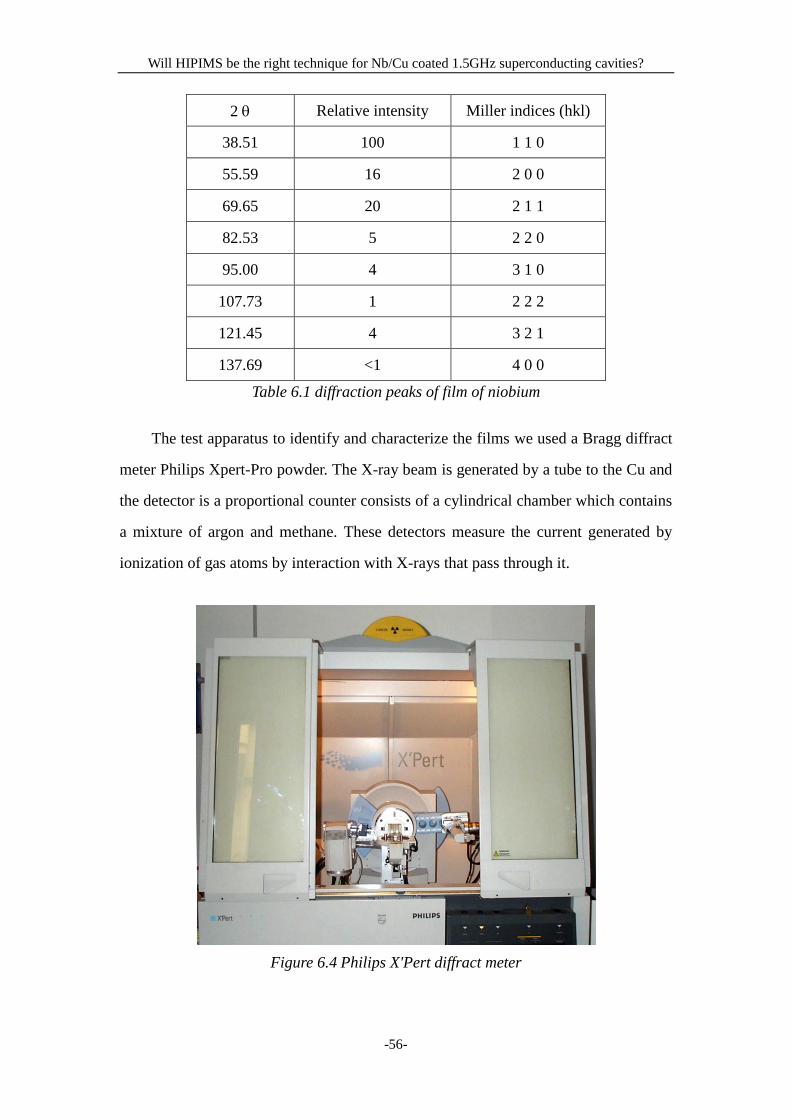
The test apparatus to identify and characterize the films we used a Bragg diffract
meter Philips Xpert-Pro powder. The X-ray beam is generated by a tube to the Cu and
the detector is a proportional counter consists of a cylindrical chamber which contains
a mixture of argon and methane. These detectors measure the current generated by
ionization of gas atoms by interaction with X-rays that pass through it.
Figure 6.4 Philips X'Pert diffract meter
Will HIPIMS be the right technique for Nb/Cu coated 1.5GHz superconducting cavities?
-57-
For the characterization of powders and bulk samples used is the standard
configuration of the diffract meter with both arms moving. For the characterization of
thin films, on the arm of the detector was mounted a collimator for analysis of thin
films from 0.18°, it consists of a series of parallel plates that restrict the viewing angle
of the incoming beam to 0.18°. The scan in this case is performed with grazing
incident beam to the sample, while the arm is moved on which is mounted on X-ray
detector.
With a quick scan type identifies the exact location of the peak (110) of niobium
for the test sample, while the film to that in the massive material and stress-free at
2=38,503° may be shifted slightly due to phenomena of stress or errors induced by
imperfect flatness of the sample or the sample holder assembly is not exactly
horizontal. Source and detector are positioned so that the sample is in a position of
reflection peak for (110), will not be changed for the duration of the measurement.
6.3 Measurement of the superconducting properties
The superconducting theory is described in chapter one. The behavior of a
superconducting material is essentially characterized by two basic parameters: The
Residual Resistivity Ratio (RRR) and the critical temperature (Tc).
The Residual Resistivity Ratio (RRR) is calculated by:
)10(
)300(
KR
KRRRR (6.4)
Since the residual strength is essentially determined by the amount of impurities
present in the sample, RRR provides an estimate of the immediate quality of the
material: the higher the more the sample is pure, that acts as a "good" superconductor. It
is also a dimensionless parameter which has the advantage of being able to leave by the
geometric dimensions that remain constant with changes in temperature and therefore
cancel out.
Will HIPIMS be the right technique for Nb/Cu coated 1.5GHz superconducting cavities?
-58-
The critical temperature is the temperature at which the sample makes the
superconducting transition, the point below which the DC electrical resistance falls,
ideally to a value below the limits of instrument sensitivity and thus can be taken as nil.
The transition temperature Tc ± ΔTc is calculated after obtaining the whole resistance
curve, using the formula:
(90%) (10%)
(90%) (10%)
2
2
c
C
T TT
T TT
(6.5)
where:
T (90%) is the temperature at which the resistance has a value equal to 90%
of that before the transition
T (10%) as the temperature at which the resistance is 10% above that of the
transition
The resistance measurement is made using the method voltage-amperage with
four points: the standard four contacts are welded, the outer two inject a sinusoidal
current, oscillating at a frequency set, while the two interior capable of measuring the
voltage drop. Applying Ohm's law R =V/I gives the resistance of the sample.
The current inversion is to avoid systematic errors due to contact resistance: if
there is a constant offset voltage V0, the measured voltage Vm, will be made by the
actual voltage V across the contacts as the offset value and therefore calculating the
resistance of the sample will be wrong. Reversing the sign of the current only affects
the voltage measured by contact and not on the offset voltage, thus mediating the
measure on the two values V1, V2 obtained with current of opposite sign should be
eliminated or at least limit the offset:
0 01 2( ) ( )
2 2m
V V V VV VV V
(6.6)
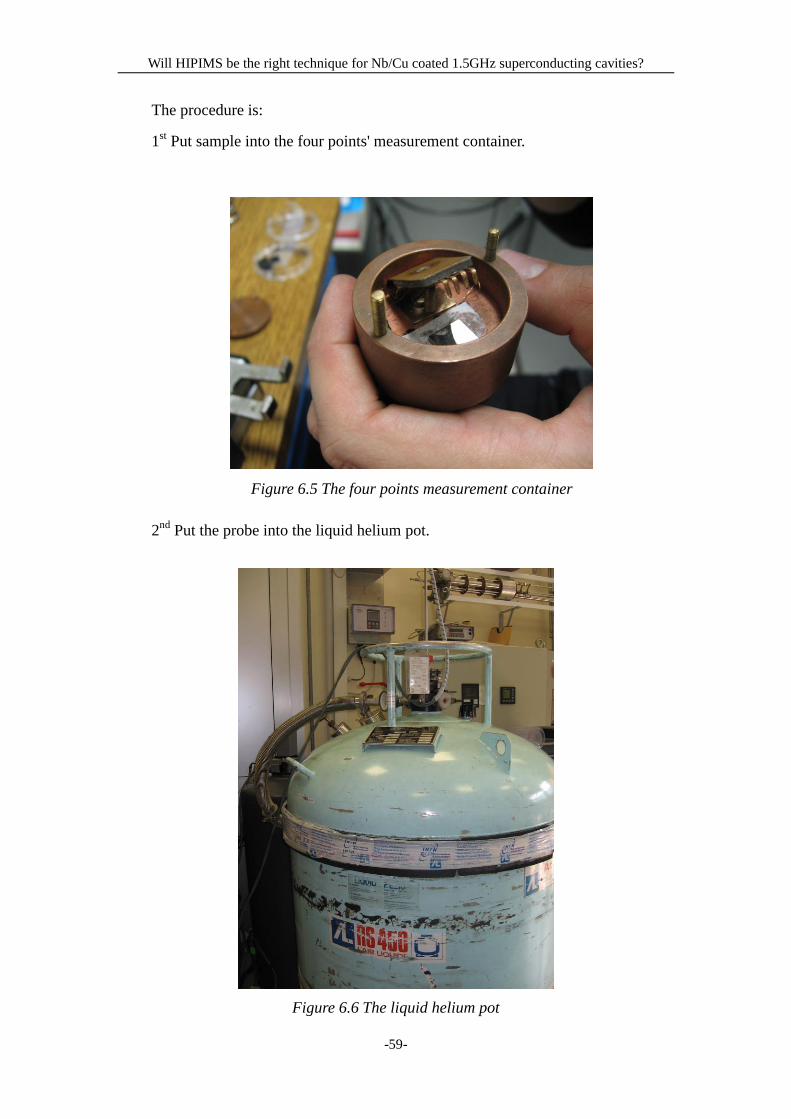
Will HIPIMS be the right technique for Nb/Cu coated 1.5GHz superconducting cavities?
-59-
The procedure is:
1st Put sample into the four points' measurement container.
Figure 6.5 The four points measurement container
2nd
Put the probe into the liquid helium pot.
Figure 6.6 The liquid helium pot
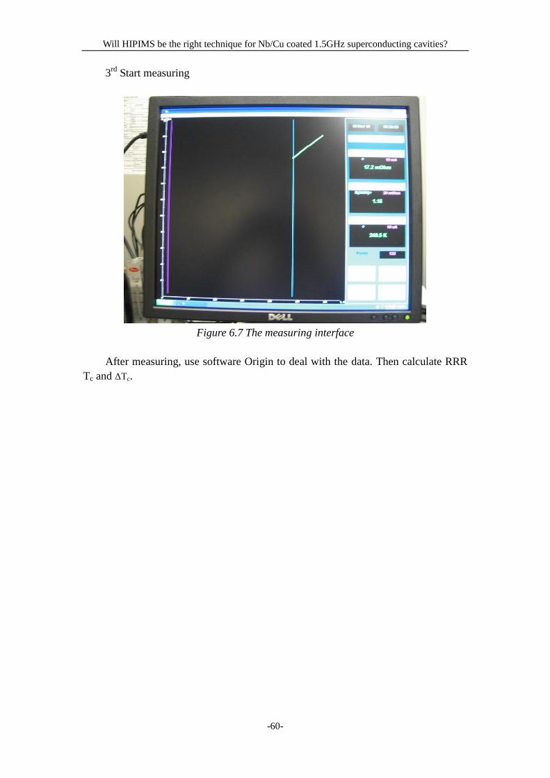
Will HIPIMS be the right technique for Nb/Cu coated 1.5GHz superconducting cavities?
-60-
3rd
Start measuring
Figure 6.7 The measuring interface
After measuring, use software Origin to deal with the data. Then calculate RRR
Tc and ΔTc.
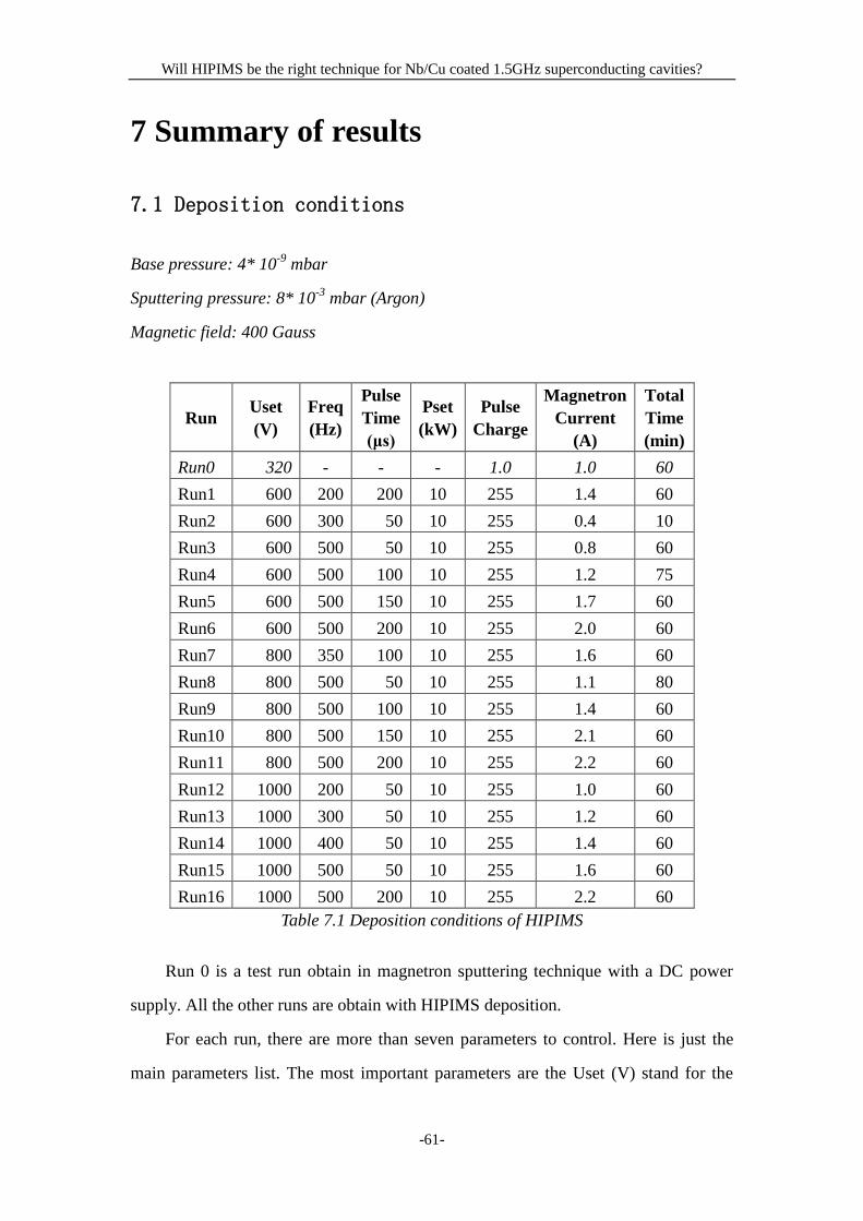
Will HIPIMS be the right technique for Nb/Cu coated 1.5GHz superconducting cavities?
-61-
7 Summary of results
7.1 Deposition conditions
Base pressure: 4* 10-9
mbar
Sputtering pressure: 8* 10-3
mbar (Argon)
Magnetic field: 400 Gauss
Run Uset
(V)
Freq
(Hz)
Pulse
Time
(μs)
Pset
(kW)
Pulse
Charge
Magnetron
Current
(A)
Total
Time
(min)
Run0 320 - - - 1.0 1.0 60
Run1 600 200 200 10 255 1.4 60
Run2 600 300 50 10 255 0.4 10
Run3 600 500 50 10 255 0.8 60
Run4 600 500 100 10 255 1.2 75
Run5 600 500 150 10 255 1.7 60
Run6 600 500 200 10 255 2.0 60
Run7 800 350 100 10 255 1.6 60
Run8 800 500 50 10 255 1.1 80
Run9 800 500 100 10 255 1.4 60
Run10 800 500 150 10 255 2.1 60
Run11 800 500 200 10 255 2.2 60
Run12 1000 200 50 10 255 1.0 60
Run13 1000 300 50 10 255 1.2 60
Run14 1000 400 50 10 255 1.4 60
Run15 1000 500 50 10 255 1.6 60
Run16 1000 500 200 10 255 2.2 60
Table 7.1 Deposition conditions of HIPIMS
Run 0 is a test run obtain in magnetron sputtering technique with a DC power
supply. All the other runs are obtain with HIPIMS deposition.
For each run, there are more than seven parameters to control. Here is just the
main parameters list. The most important parameters are the Uset (V) stand for the
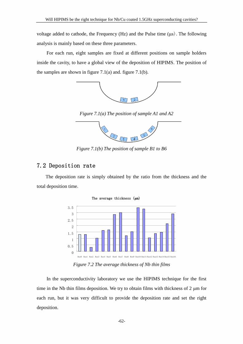
Will HIPIMS be the right technique for Nb/Cu coated 1.5GHz superconducting cavities?
-62-
voltage added to cathode, the Frequency (Hz) and the Pulse time (μs).The following
analysis is mainly based on these three parameters.
For each run, eight samples are fixed at different positions on sample holders
inside the cavity, to have a global view of the deposition of HIPIMS. The position of
the samples are shown in figure 7.1(a) and. figure 7.1(b).
Figure 7.1(a) The position of sample A1 and A2
Figure 7.1(b) The position of sample B1 to B6
7.2 Deposition rate
The deposition rate is simply obtained by the ratio from the thickness and the
total deposition time.
Figure 7.2 The average thickness of Nb thin films
In the superconductivity laboratory we use the HIPIMS technique for the first
time in the Nb thin films deposition. We try to obtain films with thickness of 2 μm for
each run, but it was very difficult to provide the deposition rate and set the right
deposition.
The average thickness (μm)
0
0.5
1
1.5
2
2.5
3
3.5
Run0 Run1 Run2 Run3 Run4 Run5 Run6 Run7 Run8 Run9 Run10 Run11 Run12 Run13 Run14 Run15 Run16
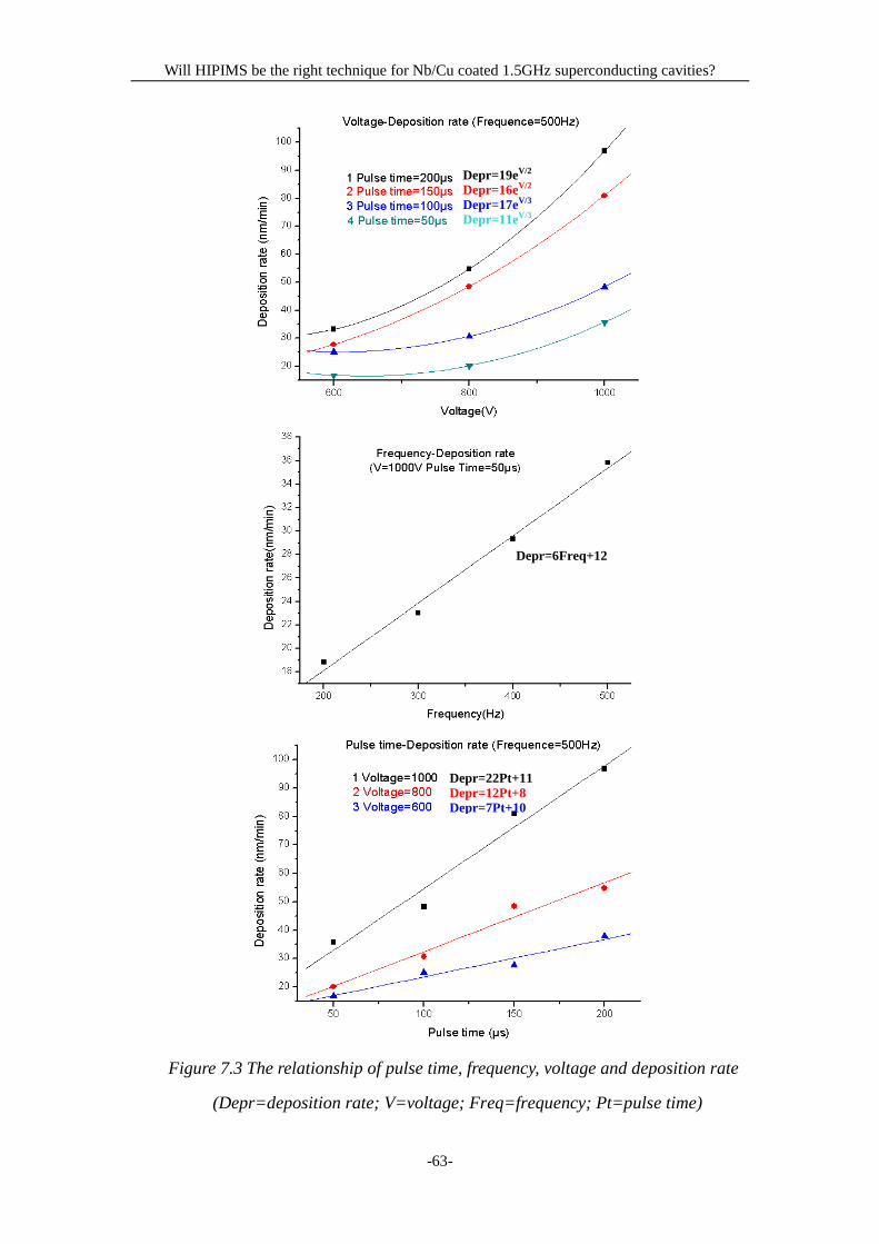
Will HIPIMS be the right technique for Nb/Cu coated 1.5GHz superconducting cavities?
-63-
Figure 7.3 The relationship of pulse time, frequency, voltage and deposition rate
(Depr=deposition rate; V=voltage; Freq=frequency; Pt=pulse time)
Depr=19eV/2
Depr=16eV/2
Depr=17eV/3
Depr=11eV/3
Depr=6Freq+12
Depr=22Pt+11 Depr=12Pt+8 Depr=7Pt+10
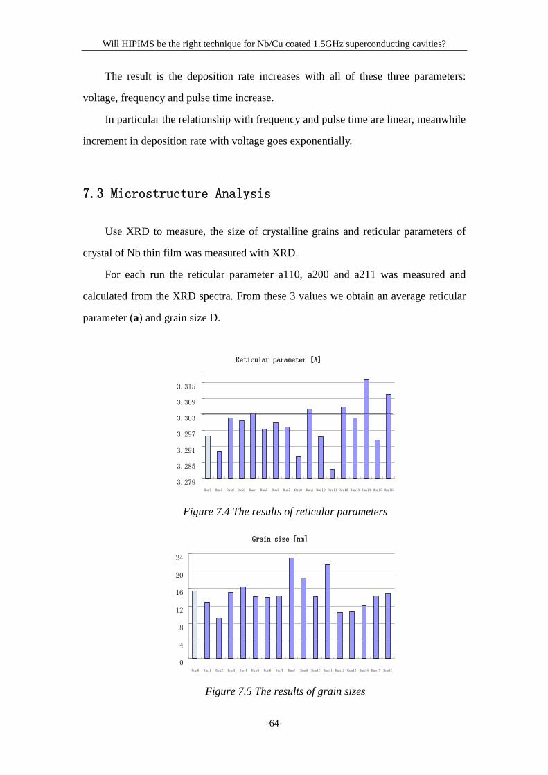
Will HIPIMS be the right technique for Nb/Cu coated 1.5GHz superconducting cavities?
-64-
The result is the deposition rate increases with all of these three parameters:
voltage, frequency and pulse time increase.
In particular the relationship with frequency and pulse time are linear, meanwhile
increment in deposition rate with voltage goes exponentially.
7.3 Microstructure Analysis
Use XRD to measure, the size of crystalline grains and reticular parameters of
crystal of Nb thin film was measured with XRD.
For each run the reticular parameter a110, a200 and a211 was measured and
calculated from the XRD spectra. From these 3 values we obtain an average reticular
parameter (a) and grain size D.
Figure 7.4 The results of reticular parameters
Figure 7.5 The results of grain sizes
Grain size [nm]
0
4
8
12
16
20
24
Run0 Run1 Run2 Run3 Run4 Run5 Run6 Run7 Run8 Run9 Run10 Run11 Run12 Run13 Run14 Run15 Run16
Reticular parameter [A]
3.279
3.285
3.291
3.297
3.303
3.309
3.315
Run0 Run1 Run2 Run3 Run4 Run5 Run6 Run7 Run8 Run9 Run10 Run11 Run12 Run13 Run14 Run15 Run16
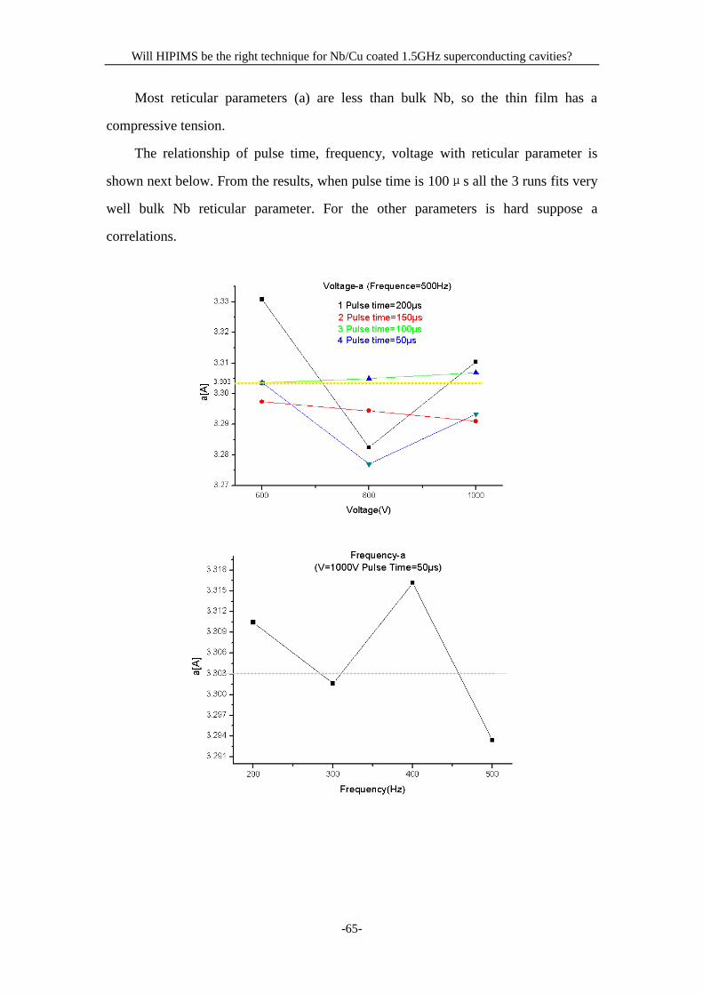
Will HIPIMS be the right technique for Nb/Cu coated 1.5GHz superconducting cavities?
-65-
Most reticular parameters (a) are less than bulk Nb, so the thin film has a
compressive tension.
The relationship of pulse time, frequency, voltage with reticular parameter is
shown next below. From the results, when pulse time is 100μs all the 3 runs fits very
well bulk Nb reticular parameter. For the other parameters is hard suppose a
correlations.
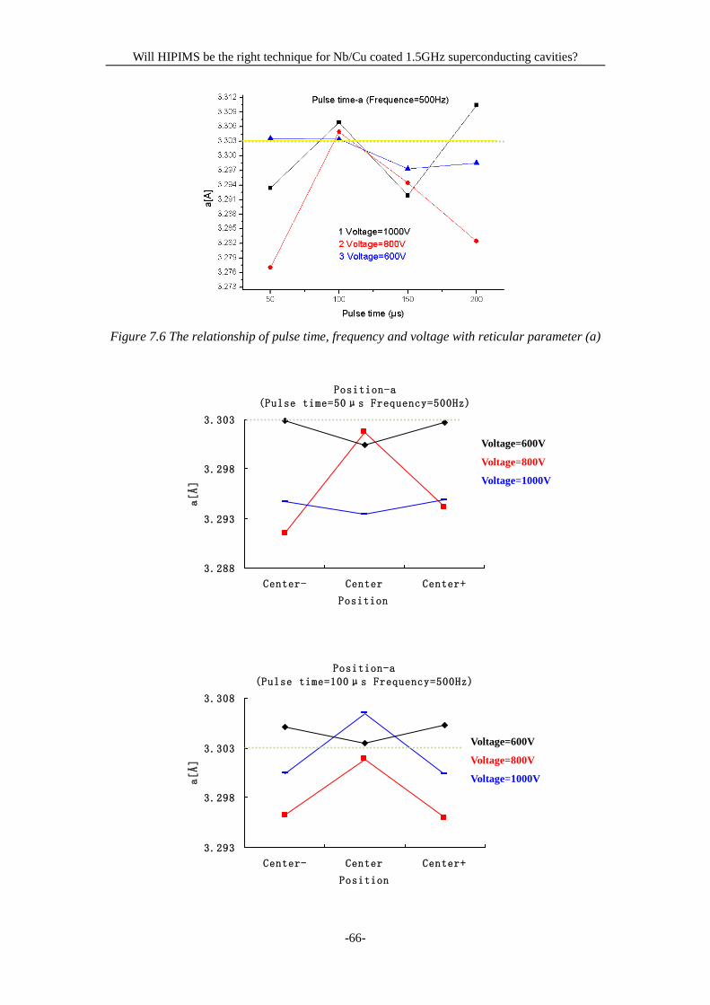
Will HIPIMS be the right technique for Nb/Cu coated 1.5GHz superconducting cavities?
-66-
Figure 7.6 The relationship of pulse time, frequency and voltage with reticular parameter (a)
Position-a
(Pulse time=50μs Frequency=500Hz)
3.288
3.293
3.298
3.303
Center- Center Center+
Position
a[Å]
Position-a
(Pulse time=100μs Frequency=500Hz)
3.293
3.298
3.303
3.308
Center- Center Center+
Position
a[Å]
Voltage=600V
Voltage=800V
Voltage=1000V
Voltage=600V
Voltage=800V
Voltage=1000V
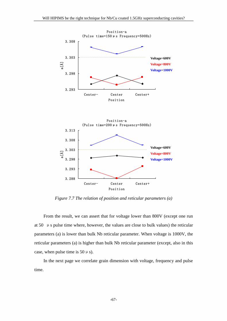
Will HIPIMS be the right technique for Nb/Cu coated 1.5GHz superconducting cavities?
-67-
Position-a
(Pulse time=150μs Frequency=500Hz)
3.293
3.298
3.303
3.308
Center- Center Center+
Position
a[Å]
Position-a
(Pulse time=200μs Frequency=500Hz)
3.288
3.293
3.298
3.303
3.308
3.313
Center- Center Center+
Position
a[Å]
Figure 7.7 The relation of position and reticular parameters (a)
From the result, we can assert that for voltage lower than 800V (except one run
at 50 μs pulse time where, however, the values are close to bulk values) the reticular
parameters (a) is lower than bulk Nb reticular parameter. When voltage is 1000V, the
reticular parameters (a) is higher than bulk Nb reticular parameter (except, also in this
case, when pulse time is 50μs).
In the next page we correlate grain dimension with voltage, frequency and pulse
time.
Voltage=600V
Voltage=800V
Voltage=1000V
Voltage=600V
Voltage=800V
Voltage=1000V
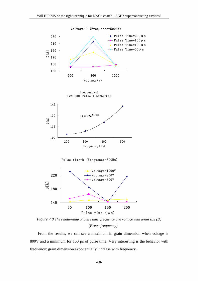
Will HIPIMS be the right technique for Nb/Cu coated 1.5GHz superconducting cavities?
-68-
Voltage-D (Frequence=500Hz)
130
150
170
190
210
230
600 800 1000
Voltage(V)
D[Å]
Pulse Time=200μs
Pulse Time=150μs
Pulse Time=100μs
Pulse Time=50μs
Frequency-D
(V=1000V Pulse Time=50μs)
100
115
130
145
200 300 400 500
Frequency(Hz)
D[Å]
Pulse time-D (Frequence=500Hz)
140
180
220
50 100 150 200
Pulse time (μs)
D[Å]
Voltage=1000V
Voltage=800V
Voltage=600V
Figure 7.8 The relationship of pulse time, frequency and voltage with grain size (D)
(Freq=frequency)
From the results, we can see a maximum in grain dimension when voltage is
800V and a minimum for 150 µs of pulse time. Very interesting is the behavior with
frequency: grain dimension exponentially increase with frequency.
D = 92e0.1Freq
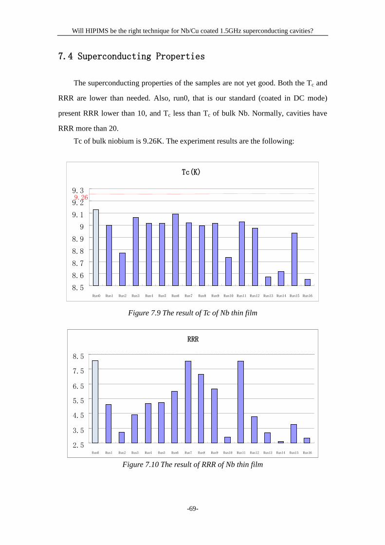
Will HIPIMS be the right technique for Nb/Cu coated 1.5GHz superconducting cavities?
-69-
7.4 Superconducting Properties
The superconducting properties of the samples are not yet good. Both the Tc and
RRR are lower than needed. Also, run0, that is our standard (coated in DC mode)
present RRR lower than 10, and Tc less than Tc of bulk Nb. Normally, cavities have
RRR more than 20.
Tc of bulk niobium is 9.26K. The experiment results are the following:
Figure 7.9 The result of Tc of Nb thin film
Figure 7.10 The result of RRR of Nb thin film
RRR
2.5
3.5
4.5
5.5
6.5
7.5
8.5
Run0 Run1 Run2 Run3 Run4 Run5 Run6 Run7 Run8 Run9 Run10 Run11 Run12 Run13 Run14 Run15 Run16
Tc(K)
8.5
8.6
8.7
8.8
8.9
9
9.1
9.2
9.3
Run0 Run1 Run2 Run3 Run4 Run5 Run6 Run7 Run8 Run9 Run10 Run11 Run12 Run13 Run14 Run15 Run16
9.26
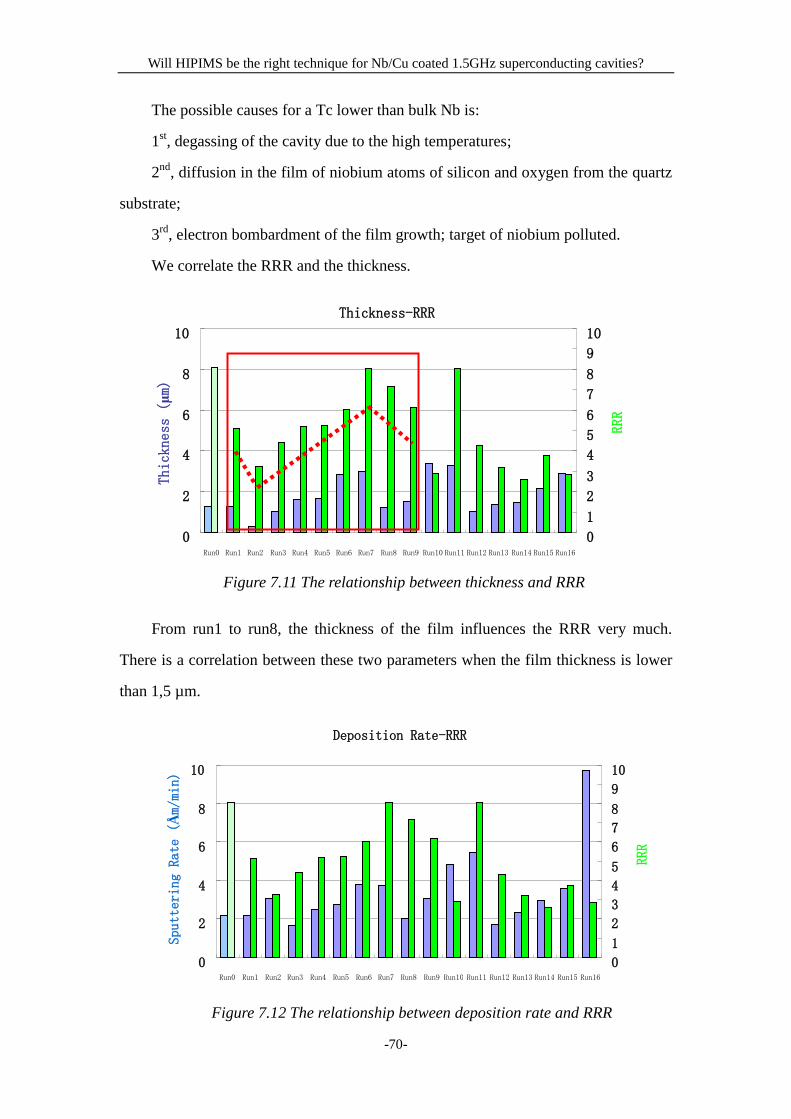
Will HIPIMS be the right technique for Nb/Cu coated 1.5GHz superconducting cavities?
-70-
The possible causes for a Tc lower than bulk Nb is:
1st, degassing of the cavity due to the high temperatures;
2nd
, diffusion in the film of niobium atoms of silicon and oxygen from the quartz
substrate;
3rd
, electron bombardment of the film growth; target of niobium polluted.
We correlate the RRR and the thickness.
Figure 7.11 The relationship between thickness and RRR
From run1 to run8, the thickness of the film influences the RRR very much.
There is a correlation between these two parameters when the film thickness is lower
than 1,5 µm.
Figure 7.12 The relationship between deposition rate and RRR
Deposition Rate-RRR
0
2
4
6
8
10
Run0 Run1 Run2 Run3 Run4 Run5 Run6 Run7 Run8 Run9 Run10 Run11 Run12 Run13 Run14 Run15 Run16
Sputtering Rate
(Åm/min)
0
1
2
3
4
5
6
7
8
9
10
RRR
Thickness-RRR
0
2
4
6
8
10
Run0 Run1 Run2 Run3 Run4 Run5 Run6 Run7 Run8 Run9 Run10 Run11 Run12 Run13 Run14 Run15 Run16
Thickness (μm)
0
1
2
3
4
5
6
7
8
9
10
RRR
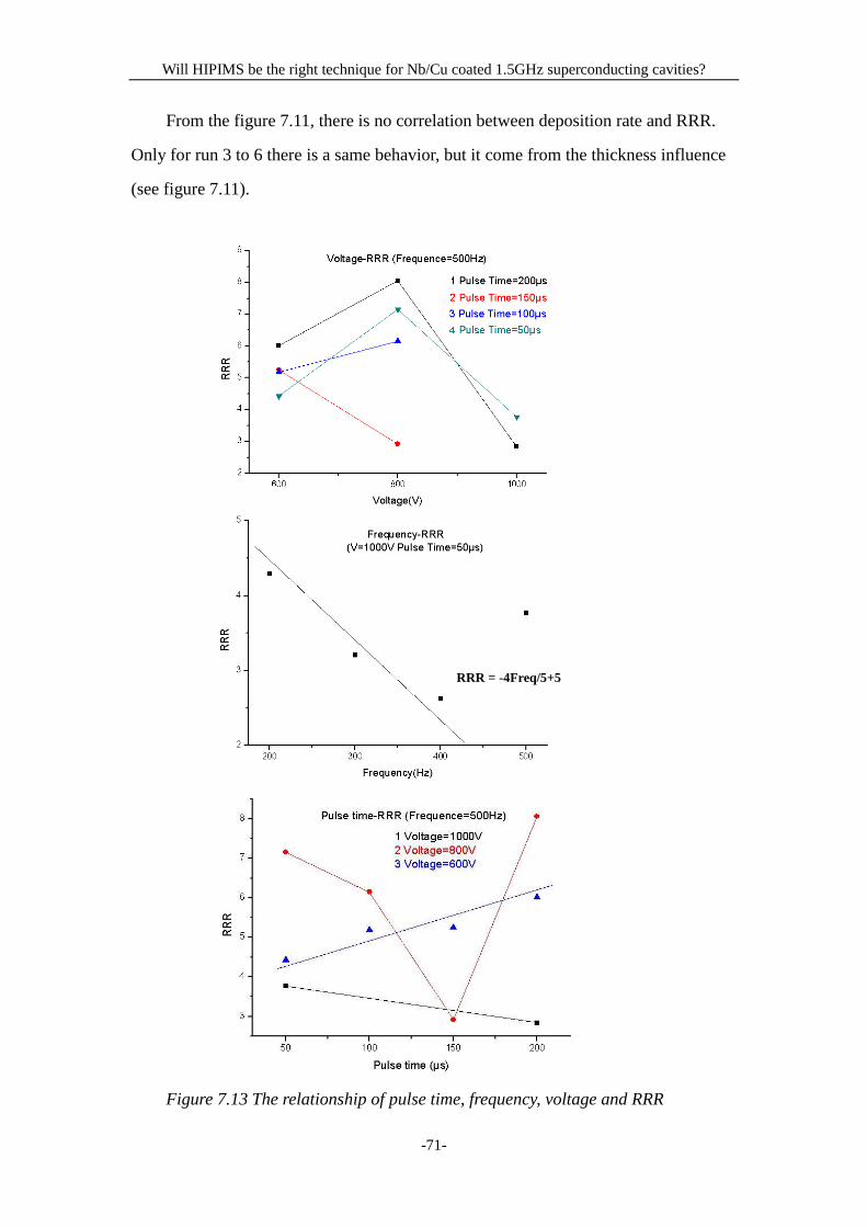
Will HIPIMS be the right technique for Nb/Cu coated 1.5GHz superconducting cavities?
-71-
From the figure 7.11, there is no correlation between deposition rate and RRR.
Only for run 3 to 6 there is a same behavior, but it come from the thickness influence
(see figure 7.11).
Figure 7.13 The relationship of pulse time, frequency, voltage and RRR
RRR = -4Freq/5+5
Will HIPIMS be the right technique for Nb/Cu coated 1.5GHz superconducting cavities?
-72-
In the previous page we correlate the RRR with voltage, frequency and pulse
time. From this graphs we arrive at the following considerations.
Voltage-RRR relationship: except for run 101 data, there is a maximum in RRR
for 800V voltage, then RRR decreases at very low values for 1000 V. We obtain the
same behavior with grain size.
Frequency-RRR relationship: RRR decreases linear with frequency. This
behavior is inverse respect grain dimension (see figure 7.8). We remove 500 Hz point
from the analysis, because in run 15 RRR is influenced from the thickness. 200, 300,
400 Hz had thickness lower than 1.5 µm; 500 Hz data have thickness higher than 2
µm. This means that the thickness uniformity is very important if you want to
understand the behavior of the RRR.
Pulse time-RRR relationship: we haven’t found relationship between pulse time
and RRR.
1 (Voltage=800V, Pulse time=150µs, Frequency=500Hz). In this run the BN insulator was changed.
The high degassing of this new important part is probably the reason of the very low RRR.
Will HIPIMS be the right technique for Nb/Cu coated 1.5GHz superconducting cavities?
-73-
8 Conclusions
During this work, HIPIMS have been developed to improve the quality of the
niobium film on copper. Finally, will be to transfer it to the deposition of cavities.
Preliminary tests were performed to understand the behavior of HIPIMS and the
parameters of the relationships between input and output.
The problem is to be suitable for works at high temperatures. Now, for each run,
we must stop when the temperature up to 200 degree (baking temperature is 220
degree). And for such a high power, it is very easy to reach that temperature.
After each run, we characterize the film from the point of view of microstructure
properties and superconducting properties.
The values of RRR and Tc of deposited films were found to be quite low. There
are some possible causes, such as degassing of the cavity due to the high temperatures,
diffusion in the film of niobium atoms of silicon and oxygen from the quartz substrate,
electron bombardment of the growing film, target of niobium polluted, etc.
We tried to correlate voltage, frequency and pulse time with microstructure and
superconductive properties and we found some characteristic behaviors:
1. the deposition rate increases with all of these three parameters: voltage,
frequency and pulse time increase. In particular the relationship with
frequency and pulse time are linear, meanwhile increment in deposition rate
with voltage goes exponentially.
2. Most reticular parameters are lower than bulk Nb value, so the thin film has a
compressive tension.
3. From the results, we can see a maximum in grain dimension when voltage is
800V and a minimum for 150 µs of pulse time. Very interesting is the behavior
with frequency: grain dimension exponentially increases with frequency.
4. The thickness of the film influences the RRR very much. There is a correlation
between these two parameters when the film thickness is lower than 1,5 µm.
Will HIPIMS be the right technique for Nb/Cu coated 1.5GHz superconducting cavities?
-74-
5. Voltage-RRR relationship: there is a maximum in RRR for 800V voltage, then
RRR decreases at very low values for 1000 V. We obtain the same behavior
with grain size.
6. Frequency-RRR relationship: RRR decreases linearly with frequency. This
behavior is opposite to the one shown by grain dimension (see figure 7.8). We
remove 500 Hz point from the analysis, because in run 15 RRR is influenced
from the thickness. 200, 300, 400 Hz had thickness lower than 1.5 µm; 500 Hz
data have thickness higher than 2 µm. This means that the thickness
uniformity is very important if you want to understand the behavior of the
RRR.
7. Pulse time-RRR relationship: we haven’t found relationship between pulse
time and RRR.
Suggestions for further research:
1st A more efficiently cooling system for the cavity; a cooling water chamber will
be done to put the cavity inside to have a better cooling condition.
2nd
, A bias will be added to improve superconducting properties. The bias
permits to lead the Nb ions produced during the HIPIMS discharge.
3rd
, Use SIMS analysis for silicon and oxygen diffuse in the film by quartz or use
sapphire substrates in place of quartz to prevent the spread of silicon and oxygen in
the film growth;
4th
, Analyze the target in order to verify the value of RRR and Tc.
Will HIPIMS be the right technique for Nb/Cu coated 1.5GHz superconducting cavities?
-75-
Will HIPIMS be the right technique for Nb/Cu coated 1.5 GHz SC Cavities?
At the end of this preliminary work with HIPIMS I will try to answer to the
difficult question on the title of thesis.
We didn’t arrive to obtain high values of RRR for our samples, maximum values
was around 9. But also in DC mode we obtained the same results in the same system,
so this means it’s not a problem of technique, but there is something wrong in our
deposition system. We talked about it before: the uncooled cathode and high
temperature reached by the cavity during the process are the principal candidates of
the film pollution. On the other hands we found that HIMPIMS parameters (in
particular voltage and frequency) influence the microstructure and the RRR of the
coated films. This means that if we found the right deposition parameters we would
obtain a high quality superconductive film.
At the moment the goal it is to identify and solve the problem of pollution of the
film, in order to obtain high RRR values. Only after having obtained high purity films,
HIPIMS can be studied deeply and used for deposition of the entire surface of the
cavity. After that the second stage of optimization of the deposition will be possible to
deposit a copper cavity and measure the features.
Will HIPIMS be the right technique for Nb/Cu coated 1.5GHz superconducting cavities?
-76-
Acknowledgements
I would like to acknowledge my supervisor: Prof. V. PALMIERI, for giving me
the great opportunity to study and work on sputtering and superconducting cavities,
making me progress, and most of all for believing in me to explore HIPIMS of Nb for
superconducting cavities.
I would like to acknowledge my Assistance supervisor: Dr. CRISTIAN PIRA,
for directing me to work and answering my questions, giving me the freedom to do
the experiments and helping me a lot on the thesis.
I would also like to thank my colleagues and friends in the Surface treatments
laboratory together: Silvia MARTIN, Giorgio KEPPEL, Winder GONZALEZ, Oscar
AZZOLINI, Antonio ROSSI, Vanessa RAMPAZZO, LI Jinhai, Dmytro CHIRKOV,
Hanieh JAHAN FAR, Iman MORADI, Giovanni TERENZIANI, and Gabriela
ACOSTA.
I am fortunate to have been working among so many talented people.
Last but not the least, I am very grateful towards my family and friends, the ones
who are still around and the ones who departed, for all the support and love you have
given me throughout all these years.
Will HIPIMS be the right technique for Nb/Cu coated 1.5GHz superconducting cavities?
-77-
References
[1] Livingston, M. Stanley & Blewett, John, Particle Accelerators, New York:
McGraw-Hill, (1962)
[2] Widerøe, R. (subscription required) Archiv Elektronik und Uebertragungstechnik
21: 387, (1928)
[3] H. Padamsee, Superconducting Sci.Technol. 14 (2001) R28–R51.
[4] Sanjay Malhotra, Method For Measuring Residual Resistivity Ratio ( RRR ) on
Standard C Bench using Keithley voltmeters
[5] B. Bonin, Materials for superconducting cavities, in: Superconductivity in Particle
Accelerators, S. Turner, CERN, May 1996, p. 191, CERN 96-03.
[6] K. Saito, P. Kneisel, Temperature Dependence of the Surface Resistance of
Niobium at 1300 MHz - Comparison to BCS Theory, in: Proceedings of the 9th
Workshop on RF Superconductivity, Santa Fe, New Mexico, USA, (1999)
[7] J. Halbritter, Calculation of the BCS surface resistance, Z. f.Phys. 238 (1970) 466.
[8] 2004 CERN Accelerator School: Superconductivity and cryogenics for
accelerators and detectors
[9] 1996 CERN Accelerator School: Superconductivity in particle accelerators
[10]1989 CERN Accelerator School: Course on superconductivity in particle
accelerators
[11]B. Aune et al., "Superconducting TESLA cavities", Phys. Rev. ST Accel. Beams
3, 092001 (2000). A thorough presentation of the many aspects of an SRF cavity
[12]2009 Conference on RF Superconductivity
[13]SRF Tutorials at the 2009 Conference on RF Superconductivity
[14] Wutz M., Adam H., Walcher W. and Steckelmacher W. Theory and Practice of
Vacuum Technology, Friedrich Vieweg & Sohn Verlag (1989)
[15]R. Behrisch (ed.) Sputtering by Particle bombardment:. Springer, Berlin. ISBN
978-3540105213, (1981)
[16] P. Sigmund, Nucl. Instr. Meth. Phys. Res. B "Mechanisms and theory of physical
sputtering by particle impact". Nuclear Instruments and Methods in Physics Research
Section B Beam Interactions with Materials and Atoms 27: 1.
doi:10.1016/0168-583X(1987)90004-8.
[17]R. Behrisch and W. Eckstein (eds.) Sputtering by Particle bombardment:
Experiments and Computer Calculations from Threshold to Mev Energies. Springer,
Berlin, (2007)
[18] L. Maissel, R. Glang, Handbook of Thin Film Technology, McGraw-Hill, New
York, (1970)
[19] Sturrock, Peter A. Plasma Physics: An Introduction to the Theory of
Astrophysical, Geophysical & Laboratory Plasmas.. Cambridge University Press.
(1994)
[20] M. Ohring Materials Science of Thin Films, Academic Press, San Diego, CA,
USA, (2002)
[21] S.M. Rossnagel in J.L. Vossen and W. Kern (eds.), Thin Film Processes II,
Will HIPIMS be the right technique for Nb/Cu coated 1.5GHz superconducting cavities?
-78-
Academic Press, New York, USA (1991)
[22] D.M. Sanders, J. Vac. Sci. Technol. A 7, 2339 (1989)
[23] D. Hoffman, R. McCune, Microstructural control of plasma sputtered refractory
coatings, in: S. Rossnagel, J. Cuomo, W. Westwoood (Eds.), Handbook of plasma
processing technology, Noyes publications, (1990)
[24] B. Movchan, A. Demchishin, Study of the structure and properties of thin
vacuum condenstaes of nickel, titaniom, tungsten, aluminium oxide, and zirconium
oxide, Fiz.Metal.Metalloved 28 (1969) 653.
[25] L. Maissel, P. Schaible, Thin Films Deposited by Bias Sputtering, J.Appl.Phys.
36 (1965) 237.
[26] J. Thornton, Influence of apparatus geometry and deposition conditions on the
structure and topography of thick sputtered coatings, Journ. of Vacuum Sci. and Tech.
11 (1974) 666.
[27] A. C. Raghuram, R. F. Bunshah, Journ. of Vacuum Sci. and Tech. 9 (1974) 1389.
[28] G. Orlandi, C. Benvenuti, S. Calatroni, F. Scalambrin, Expected dependence of
Nbcoated RF cavity performance on the characteristics of niobium, in: Proceedings of
the 6th Workshop on RF Superconductivity, CEBAF, USA, (1993)
[29] G. M. Schucan, C. Benvenuti, S. Calatroni, Niobium films produced by
magnetron sputtering using an Ar-He mixture as discharge gas, note 94-23.
[30] C. Benvenuti et. al., Rare gas trapping in sputtered Nb films, in: Proceedings of
the 7th Workshop on RF Superconductivity, Gif-sur-Yevette, France, (1995)
[31] V. Kouznetsov, K. Macák, J.M. Schneider, U. Helmersson, and I. Petrov, Surf.
Coat. Technol. 122, 290, (1999)
[32] K. Macák, V. Kouznetsov, J. Schneider, U. Helmersson, and I. Petrov, J. Vac.
Sci. Technol. A 18, 1533, (2000)
[33] V. Kouznetsov, U.S. Patent No. 6,296,742 B1, (2001)
[34] V. Kouznetsov, US Patent 2004/0020760 A1, (2004)
[35] V. Kouznetsov, Swedish Patent 525231, (2005)
[36] V. Kouznetsov, WO 2005/005684 A1, (2005)
[37] A.P. Ehiasarian, R. New, W.-D. Münz, L. Hultman, U. Helmersson, and V.
Kouznetsov, Vacuum 65, 147, (2002)
[38] V. Kouznetsov, U.S. Patent No. 6,296,742 B1 (2001)
[39] D.J. Christie, W.D. Sproul, D.C. Carter, and F. Tomasel, Proceedings of the 47th
Annual Technical Conference Proceedings of the Society of Vacuum Coaters, 113
(2004)
[40] D.J. Christie, F. Tomasel, W.D. Sproul, and D.C. Carter, J. Vac. Sci. Technol. A
22,1415 (2004)
[41] B.M. DeKoven, P.R. Ward, and R.E. Weiss, D.J. Christie, R.A. Scholl, W.D.
Sproul, F. Tomasel, and A. Anders, Proceedings of the 46th Annual Technical
Conference Proceedings of the Society of Vacuum Coaters, 158, (2003)
[42] W.D. Sproul, D.J. Christie, and D.C. Carter, Proceedings of the 47th Annual
Technical Conference of the Society of Vacuum Coaters, 96, (2004)
[43] J. Alami, Dissertation No 948, Linköping Studies in Science and Technology,
(2005)
Will HIPIMS be the right technique for Nb/Cu coated 1.5GHz superconducting cavities?
-79-
[44] J. Alami, P.O.Å. Persson, D. Music, J.T. Gudmundsson, J. Bohlmark, and U.
Helmersson, J. Vac. Sci. Technol. A 23, 278, (2005)
[45] A.P. Ehiasarian et al., Vacuum 65 (2002) 147154
[46] J. Alami et al., J. Vac. Sci. Technol. A 23 (2005) 278
[47] J. Alami et al., Thin Solid Films 515 (2006) 1731
[48] C. Benvenuti et al., Physica C 316 (1999) 153
[49] S.P. Bugaev, N.N. Koval, N.S. Sochugov, and A.N. Zakharov, Proceedings of
the XVIIth International Symposium on Discharges and Electrical Insulation in
Vacuum, 1074, (1996)
[50] J.A. Davis, W.D. Sproul, D.J. Christie, and M. Geisler, Proceedings of the 47th
Annual Technical Conference Proceedings of the Society of Vacuum Coaters, 215,
(2004)