Embed Size (px)
Citation preview
The effects of semicon on space charge behaviour
under different temperature conditions for
HVDC cable insulation
M. Hao, A. Fazal, A. S. Vaughan, G. Chen
Tony Davis High Voltage Laboratory
University of Southampton
Southampton, SOl7 lBJ, UK
H. Wang, C. Zhang, Y. Zhou
Global Energy Interconnection Research Institute
Beijing, China
Abstract—One of the major concerns related to HVDC
applications is the presence of space charge within the dielectrics,
which distorts the electric field distribution and contributes to
accelerated ageing and consequent failure of the cable insulation.
In this paper, an attempt is made to explore the space charge
characteristics using different electrode materials and
temperature conditions to highlight the variation in space charge
formation and distribution in the system using pulsed electro
acoustic (PEA) technique. To simulate a real cable manufacturing
process, XLPE insulation was sandwiched between two layers of
thermal bonded semicon material. The experimental results
revealed that the semiconductive materials has a greater influence
on the space charge formation. It was found the electrode
materials play a vital role in determining the charge distribution
in the insulation and significant dependence on the electrode
materials under the same applied stress and temperature
conditions. Thermal bonded semicon samples have a stronger
charge injection and greater charge amount within the bulk and
high temperature can greatly increase the charge mobility for both
polarities as well as enhances charge injection. These findings are
discussed in conjunction with unbonded sample (conventional
setup) for the space charge measurements.
Keywords — Space charge; PEA; XLPE; HVDC cable;
semiconducting material; charge injection
I. INTRODUCTION
Polyethylene (PE) base insulation is most widely used in
high voltage direct current (HVDC) transmission. In most
applications, it is essential to modify PE material to enhance
certain properties. For example, introducing crosslinks between
the polymer chains in which a network is formed thereby
improving heat and chemical resistance, stress cracking and
shrinkage as well as excellent dielectric strength and electrical
resistivity [1]. This has resulted crosslinked polyethylene
(XLPE) as the most common polymeric insulation used in
power transmission up to 500 kV [2]. The typical construction
of power cables includes a conductor surrounded by insulation
and semi-conductive (semicon) screens. The semicon provides
a smooth interface between the insulation and the conducting
parts, thus preventing the concentration of electrical stress
within the insulation material. For insulation materials, XLPE
offers key characteristics including low dielectric loss and high
breakdown strength. Although, most polymers are excellent
electrical insulators, charge carriers do exist with these
materials [3]. For example, accumulation of space charge in the
insulating material is one of the cause for unexpected
breakdown [4]. It has been reported extensively in the literature
that the space charge can be formed in polymeric insulation
under DC conditions and this poses a threat to the reliability of
the cable [5]. For DC applications, space charge in the XLPE
insulation material is a major concern and it is known to affect
electrical conduction and can distort the electric field
distribution in the system [6, 7]. Moreover, the localized charge
trapping caused by the crosslinking byproducts can result in
increased space charge accumulations and leading to the
enhancement of local electric field distortions in XLPE [5, 8,
9]. The enhanced electric stress could further cause breakdown,
particularly, under the operational high temperature [10-12].
The future development in HVDC XLPE insulated cables
requires a fundamental understanding of potential failure
mechanisms and for this reason studies on space charge
formation under the conditions of different semicon electrode
material and temperature is vital for understanding the space
charge characteristics of the insulation material. For the space
charge characteristics, PEA method is most widely used for
HVDC cables and it has been recognized that the electrodes
have a significant effect on the space charge formation and
dynamics [13, 14]. This technique utilizes interaction between
high voltage pulses and charge layers accumulated in the
insulating material to produce acoustic pressure waves, which
transverse across the material [15].
By focusing on different semicon electrode materials, this
paper reports on the space charge dynamics under DC electric
stress at various temperature conditions using PEA technique.
With the aim to simulate the structure of a real power cable,
XLPE samples were sandwiched between two layers of HVDC
cable grade semi-conductive material. This was necessary as
the traditional PEA arrangement may not represent the real
extruded HVDC cable, where the semi-conductive material is
thermal bonded to the insulation.

II. EXPERIMENTAL
A. Materials
The samples used in this study were produced from HV cable-grade low density polyethylene (LDPE) and two types of semicon materials were from the same grade loaded with carbon black. Insulating materials were supplied by the Smart Grid Research Institute (China) and the crosslinking agent dicumyl peroxide (DCP) was supplied by Sigma-Aldrich.
B. Sample Preparation
The LDPE and DCP (2 %) were first mixed in bulk at 120 ℃ for 15 min in a Thermo PolyLab mixer. Samples of the resulting LDPE containing DCP (~250 µm thickness) and the semicon (~50 µm thickness) were separately prepared by hot pressing at temperature below the activation threshold of the crosslinking agent. Crosslinking was achieved by hot-pressing the electrodes and the insulating bulk at 200 ℃ for 10 min, schematically illustrated in Fig. 1. The resultant thickness of the samples was approximately 250 µm. For sample preparation, both materials were allowed to melt for 2 min at 120 ℃, this was essential to ensure good bonding. The applied load was maintained during the cooling process and the sample was removed from the hot press once 120 ℃ reached and further cooled down to room temperature. To remove volatile residual byproducts, XLPE samples were left in a vacuum oven for 6 days at a constant temperature of 80 ℃. The samples were then cooled down to room temperature and sealed in polyethylene bags, ready for the tests.
Fig. 1. Schematic illustration of the semicon electrode setups used for PEA and conductivity measurements.
C. Sample Characterization
Space charge distributions under different electrode systems were measured using the PEA system. The PEA method consists in applying a voltage pulse as perturbation across the sample, which generates acoustic force from the interaction with the electrostatic stress induced by the space charge [12]. For this, the sample was inserted between the lower and upper electrodes and DC electric field of 40 kV/mm was applied at 25 ℃ and 60 ℃, respectively. Space charge data were acquired both with the field applied to the sample and during its subsequent decay under short circuit conditions. The evolution of charge, polarization (voltage on) and depolarization (voltage off) for each stressing period lasted 60 mins. The calibration for PEA tests was done by applying a low voltage (2 kV) for a short period of time (5 s) to show the capacitive charges on both electrodes. This low voltage was chosen to ensure no space charge developed in the bulk sample.
In order to show the charge build-up process during the volts-on tests, the normalization has to be made on the result data. Similar with Liu et al studies [16], subtraction method was employed to remove capacitive charges from the system. In this method, the actual measured charge density data obtained from the volts-on measurement are subtracted from the reference to reveal the injected charges in the sample and its induced image charge at the electrodes. As the applied voltage of reference data was lower, therefore, the reference data was multiplied to obtain equivalent applied voltage that can be considered as the charge density data without effect of the space charges in the bulk.
III. RESULTS AND DISCUSSION
A. Space Charge Measurments at Room Temperature
Fig. 2 shows the space charge evolution from XLPE sample using the conventional PEA setup at room temperature, i.e aluminum (Al) as the cathode and unbonded semicon (Sc) as the anode. The formation of heterocharge can be observed adjacent to the Al electrode and the positive charges build up quickly in the first 5 mins after voltage application and then gradually stabilizes. The presence of heterocharges are usually formed by the crosslinking by-products or impurities within the insulation material [5], suggesting the residual by-products after the degassing process still dominate the space charge behavior in the sample material. After the removal of the applied voltage, only positive charges are remained in the sample bulk, inducing the negative charges on the two electrodes. The positive peak adjacent to the cathode decreases from 5.1 Cm-3 to 3.1 Cm-3 after 1 hour decay time.
Thermal bonded semicon electrode
Thermal bonded
semicon electrode
ANODE
CATHODE
XLPE
Fig. 2. PEA charge density profile of XLPE (degassed) unbonded semicon/Aluminum electrodes. The applied voltage was 40 kV/mm at
temperature of 25 ℃.
-30
-20
-10
0
10
20
30
-50 0 50 100 150 200
Char
ge
den
sity
(C
m-3
)
Thickness (µm)
Voltage ON (Normalized)
0 min 0.5 min
1 min 2 min
5 min 10 min
15 min 30 min
45 min 60 min
-15
-5
5
15
-50 0 50 100 150 200
Char
ge
den
sity
(C
m-3
)
Thickness (µm)
Voltage OFF
0.5 min 1 min5 min 10 min15 min 30 min45 min 60 min
Cathode
(Al)
Anode (Sc)
Cathode
(Al)
Anode
(Sc)
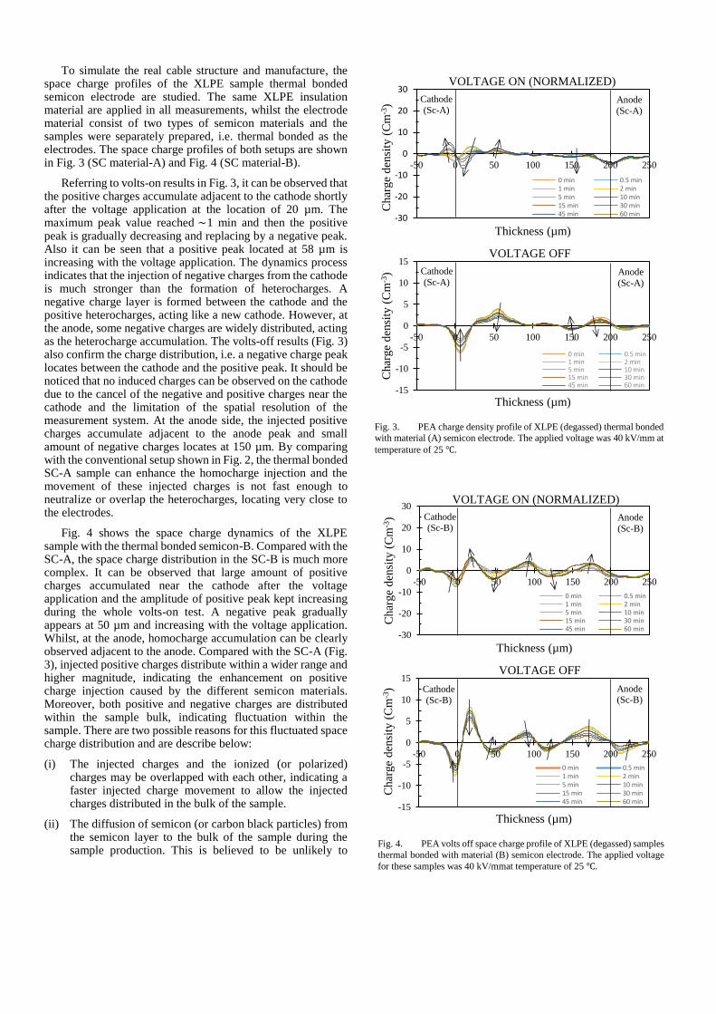
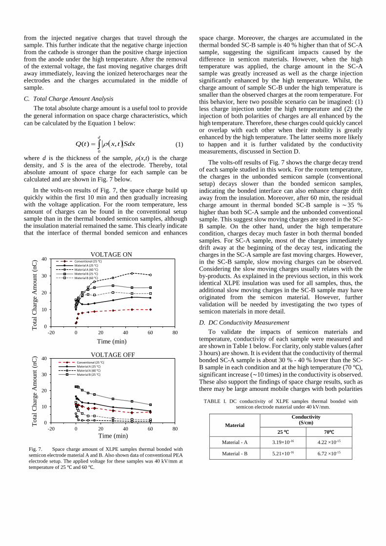
To simulate the real cable structure and manufacture, the space charge profiles of the XLPE sample thermal bonded semicon electrode are studied. The same XLPE insulation material are applied in all measurements, whilst the electrode material consist of two types of semicon materials and the samples were separately prepared, i.e. thermal bonded as the electrodes. The space charge profiles of both setups are shown in Fig. 3 (SC material-A) and Fig. 4 (SC material-B).
Referring to volts-on results in Fig. 3, it can be observed that the positive charges accumulate adjacent to the cathode shortly after the voltage application at the location of 20 µm. The maximum peak value reached ~1 min and then the positive peak is gradually decreasing and replacing by a negative peak. Also it can be seen that a positive peak located at 58 µm is increasing with the voltage application. The dynamics process indicates that the injection of negative charges from the cathode is much stronger than the formation of heterocharges. A negative charge layer is formed between the cathode and the positive heterocharges, acting like a new cathode. However, at the anode, some negative charges are widely distributed, acting as the heterocharge accumulation. The volts-off results (Fig. 3) also confirm the charge distribution, i.e. a negative charge peak locates between the cathode and the positive peak. It should be noticed that no induced charges can be observed on the cathode due to the cancel of the negative and positive charges near the cathode and the limitation of the spatial resolution of the measurement system. At the anode side, the injected positive charges accumulate adjacent to the anode peak and small amount of negative charges locates at 150 µm. By comparing with the conventional setup shown in Fig. 2, the thermal bonded SC-A sample can enhance the homocharge injection and the movement of these injected charges is not fast enough to neutralize or overlap the heterocharges, locating very close to the electrodes.
Fig. 4 shows the space charge dynamics of the XLPE sample with the thermal bonded semicon-B. Compared with the SC-A, the space charge distribution in the SC-B is much more complex. It can be observed that large amount of positive charges accumulated near the cathode after the voltage application and the amplitude of positive peak kept increasing during the whole volts-on test. A negative peak gradually appears at 50 µm and increasing with the voltage application. Whilst, at the anode, homocharge accumulation can be clearly observed adjacent to the anode. Compared with the SC-A (Fig. 3), injected positive charges distribute within a wider range and higher magnitude, indicating the enhancement on positive charge injection caused by the different semicon materials. Moreover, both positive and negative charges are distributed within the sample bulk, indicating fluctuation within the sample. There are two possible reasons for this fluctuated space charge distribution and are describe below:
(i) The injected charges and the ionized (or polarized) charges may be overlapped with each other, indicating a faster injected charge movement to allow the injected charges distributed in the bulk of the sample.
(ii) The diffusion of semicon (or carbon black particles) from the semicon layer to the bulk of the sample during the sample production. This is believed to be unlikely to
Fig. 3. PEA charge density profile of XLPE (degassed) thermal bonded
with material (A) semicon electrode. The applied voltage was 40 kV/mm at
temperature of 25 ℃.
-30
-20
-10
0
10
20
30
-50 0 50 100 150 200 250
Char
ge
den
sity
(C
m-3
)
Thickness (µm)
VOLTAGE ON (NORMALIZED)
0 min 0.5 min1 min 2 min5 min 10 min15 min 30 min45 min 60 min
-15
-10
-5
0
5
10
15
-50 0 50 100 150 200 250
Char
ge
den
sity
(C
m-3
)
Thickness (µm)
VOLTAGE OFF
0 min 0.5 min1 min 2 min5 min 10 min15 min 30 min45 min 60 min
Fig. 4. PEA volts off space charge profile of XLPE (degassed) samples
thermal bonded with material (B) semicon electrode. The applied voltage
for these samples was 40 kV/mmat temperature of 25 ℃.
-30
-20
-10
0
10
20
30
-50 0 50 100 150 200 250
Char
ge
den
sity
(C
m-3
)
Thickness (µm)
VOLTAGE ON (NORMALIZED)
0 min 0.5 min1 min 2 min5 min 10 min15 min 30 min45 min 60 min
-15
-10
-5
0
5
10
15
-50 0 50 100 150 200 250
Char
ge
den
sity
(C
m-3
)
Thickness (µm)
VOLTAGE OFF
0 min 0.5 min1 min 2 min5 min 10 min15 min 30 min45 min 60 min
Cathode
(Sc-A) Anode
(Sc-A)
Cathode
(Sc-A) Anode
(Sc-A)
Cathode (Sc-B)
Anode
(Sc-B)
Cathode
(Sc-B)
Anode (Sc-B)

happen as all the sample preparation process remained the same for both semicon material. However, further validation would be required to confirm this phenomena. It is worth noting that the volts-off results also confirms the fluctuation of the space charge distribution within the sample bulk.
B. Space Charge Measurments At High Temperature
To investigate the space charge characteristics under the high temperature condition, the PEA measurement system was placed in a fan oven and the application of external voltage and the space charge measurement were obtained once the temperature stabilized at 60 ℃.
Fig 5 shows the space charge profiles in the XLPE sample with thermal bonded SC-A under high temperature. It can be observed that the negative charges accumulation dominate the space charge distribution within the sample. These negative charges mainly distribute in two regions near the electrodes. At the cathode side, large amount of negative charges are injected and moving towards bulk of the sample. The movement of the negative charges was greatly enhanced by the high temperature, i.e. the negative charge distribution is quickly increased from a small region near the cathode to a much boarder region within the bulk. On the other hand, negative charges also accumulate at the anode side and these negative charges are gradually moving towards to the anode. The origins of these negative charges may have come from two aspects: (1). the ionization (or polarization) of the by-products within the XLPE sample and (2). the injected negative charges from the cathode move through the sample as these charge movement has been greatly enhanced and accumulate at the interface between the semicon and the insulation. These two origins may occur at the same time. For example, when the external voltage was removed, shown in the volts-off results (Fig. 5), most of the charges that can be observed in the volts-on results are quickly disappeared within few seconds. And almost after 3 min, negative charges are all drift away and only remained a small positive peak adjacent to the cathode. The charge dynamics in the decay process indicate that the charge injection and ionization occur at the same time in the sample, however, the negative charge injection dominates the space charge behavior. These injected negative charges generally have a high charge mobility and overlapped with the ionized positive charges until they drift away from the sample.
The space charge profiles of the XLPE thermal bonded with the SC-B under high temperature are shown in Fig. 6. It can be seen that when the external voltage is applied, heterocharge accumulation occurs at the both electrodes. At the cathode side, the positive charges are quickly decreasing with the voltage application due to the negative charge injection from the cathode. However, the injected negative charges do not fully cancel the accumulated positive charge near the cathode, but quickly move to the middle of the sample at 100 µm (combined with the positive charges injected from the anode). On the other hand, the negative charges accumulated in region adjacent to the anode keeps increasing with the voltage application. Considering the fact that some of the positive charges accumulated in the middle of the sample should be injected from the anode, those increased negative charges may result
Fig. 5. PEA volts off space charge profile of XLPE (degassed) samples
thermal bonded with material (A) semicon electrode. The applied voltage
for these samples was 40 kV/mmat temperature of 60 ℃.
-30
-20
-10
0
10
20
30
-50 0 50 100 150 200 250
Char
ge
den
sity
(C
m-3
)
Thickness (µm)
VOLTAGE ON (NORMALIZED)
0 min 0.5 min1 min 2 min5 min 10 min15 min 30 min45 min 60 min
-15
-10
-5
0
5
10
15
-50 0 50 100 150 200 250
Char
ge
den
sity
(C
m-3
)Thickness (µm)
Voltage OFF
0 min 0.5 min1 min 2 min5 min 10 min15 min 30 min45 min 60 min
Fig. 6. PEA volts off space charge profile of XLPE (degassed) samples thermal bonded with material (B) semicon electrode. The applied voltage
for these samples was 40 kV/mm at temperature of 60 ℃.
-30
-20
-10
0
10
20
30
-50 0 50 100 150 200 250
Char
ge
den
sity
(C
m-3
)
Thickness (µm)
VOLTAGE ON (NORMALIZED)
0 min 0.5 min1 min 2 min5 min 10 min15 min 30 min45 min 60 min
-15
-10
-5
0
5
10
15
-50 0 50 100 150 200 250
Char
ge
den
sity
(C
m-3
)
Thickness (µm)
VOLTAGE OFF
0 min 0.5 min1 min 2 min5 min 10 min15 min 30 min45 min 60 min
Cathode
(Sc-A)
Anode
(Sc-A)
Cathode
(Sc-A) Anode
(Sc-A)
Cathode
(Sc-B)
Anode
(Sc-B)
Cathode
(Sc-B) Anode
(Sc-B)
from the injected negative charges that travel through the sample. This further indicate that the negative charge injection from the cathode is stronger than the positive charge injection from the anode under the high temperature. After the removal of the external voltage, the fast moving negative charges drift away immediately, leaving the ionized heterocharges near the electrodes and the charges accumulated in the middle of sample.
C. Total Charge Amount Analysis
The total absolute charge amount is a useful tool to provide
the general information on space charge characteristics, which
can be calculated by the Equation 1 below:
d
SdxtxtQ0
,)( (1)
where d is the thickness of the sample, ρ(x,t) is the charge density, and S is the area of the electrode. Thereby, total absolute amount of space charge for each sample can be calculated and are shown in Fig. 7 below.
In the volts-on results of Fig. 7, the space charge build up quickly within the first 10 min and then gradually increasing with the voltage application. For the room temperature, less amount of charges can be found in the conventional setup sample than in the thermal bonded semicon samples, although the insulation material remained the same. This clearly indicate that the interface of thermal bonded semicon and enhances
space charge. Moreover, the charges are accumulated in the thermal bonded SC-B sample is 40 % higher than that of SC-A sample, suggesting the significant impacts caused by the difference in semicon materials. However, when the high temperature was applied, the charge amount in the SC-A sample was greatly increased as well as the charge injection significantly enhanced by the high temperature. Whilst, the charge amount of sample SC-B under the high temperature is smaller than the observed charges at the room temperature. For this behavior, here two possible scenario can be imagined: (1) less charge injection under the high temperature and (2) the injection of both polarities of charges are all enhanced by the high temperature. Therefore, these charges could quickly cancel or overlap with each other when their mobility is greatly enhanced by the high temperature. The latter seems more likely to happen and it is further validated by the conductivity measurements, discussed in Section D.
The volts-off results of Fig. 7 shows the charge decay trend of each sample studied in this work. For the room temperature, the charges in the unbonded semicon sample (conventional setup) decays slower than the bonded semicon samples, indicating the bonded interface can also enhance charge drift away from the insulation. Moreover, after 60 min, the residual charge amount in thermal bonded SC-B sample is ~35 % higher than both SC-A sample and the unbonded conventional sample. This suggest slow moving charges are stored in the SC-B sample. On the other hand, under the high temperature condition, charges decay much faster in both thermal bonded samples. For SC-A sample, most of the charges immediately drift away at the beginning of the decay test, indicating the charges in the SC-A sample are fast moving charges. However, in the SC-B sample, slow moving charges can be observed. Considering the slow moving charges usually relates with the by-products. As explained in the previous section, in this work identical XLPE insulation was used for all samples, thus, the additional slow moving charges in the SC-B sample may have originated from the semicon material. However, further validation will be needed by investigating the two types of semicon materials in more detail.
D. DC Conductivity Measurement
To validate the impacts of semicon materials and temperature, conductivity of each sample were measured and are shown in Table 1 below. For clarity, only stable values (after 3 hours) are shown. It is evident that the conductivity of thermal bonded SC-A sample is about 30 % - 40 % lower than the SC-B sample in each condition and at the high temperature (70 ℃), significant increase (~10 times) in the conductivity is observed. These also support the findings of space charge results, such as there may be large amount mobile charges with both polarities
TABLE I. DC conductivity of XLPE samples thermal bonded with semicon electrode material under 40 kV/mm.
Material
Conductivity (S/cm)
25 ℃ 70℃
Material - A 3.19×10⁻¹⁶ 4.22 ×10⁻¹⁵
Material - B 5.21×10⁻¹⁶ 6.72 ×10⁻¹⁵
Fig. 7. Space charge amount of XLPE samples thermal bonded with
semicon electrode material A and B. Also shown data of conventional PEA
electrode setup. The applied voltage for these samples was 40 kV/mm at
temperature of 25 ℃ and 60 ℃.
0
10
20
30
40
-20 0 20 40 60 80
To
tal
Char
ge
Am
ount
(nC
)
Time (min)
VOLTAGE ONConventional (25 ℃)
Material A (25 ℃)
Material A (60 ℃)
Material B (25 ℃)
Material B (60 ℃)
0
10
20
30
40
-20 0 20 40 60 80
To
tal
Char
ge
Am
ount
(nC
)
Time (min)
VOLTAGE OFFConventional (25 ℃)Material A (25 ℃)Material A (60 ℃)Material B (25 ℃)

within the SC-B samples under the high temperature. However, these mobile charges are difficult to be distinguished by the PEA system due to the cancel or overlap of the charges.
IV. CONCLUSIONS
In this paper, the impacts of thermal bonded semicon material on XLPE insulation under different temperatures are investigated and discussed. In order to simulate the real cable structure and manufacture process, a new sample manufacture method-XLPE with thermal bonded semicon is introduced and applied for space charge and conductivity measurements. The results are also compared with the unbonded sample (conventional setup) for the space charge measurements. The
conclusions are expressed as follows:
1. Comparing conventional setup for the space charge measurement, the thermal bonded semicon samples generally shows a stronger charge injection and this resulted in a larger charge amount within the bulk. This suggest that the space charge characteristics in the real cable could be worse than the conventional setup used in the laboratory.
2. The experimental results of both space charge and conductivity have shown significant impacts using a different semicon materials bonded with the XLPE insulation: such as semicon material-A used in this work leads to a relative less charge injection, especially positive charge injection and semicon material-B has the lowest smaller conductivity.
3. The high temperature can greatly increase the charge mobility for both polarities as well as enhances charge injection. Moreover, the impacts of high temperature are different on the dielectric performance in the two different semicon bonded samples.
The detailed investigations on the semicon materials, and the principle of their impacts on the full scale cable insulation system will be further investigated in future.
ACKNOWLEDGMENT
The authors are grateful for the financial support from the State Grid Cooperation of China: Research on Key Technologies of Insulation Material and Accessories for 320 kV HVDC XLPE Cable System (SGRIZLJS(2014)888).
REFERENCES
[1] A. Smedberg, T. Hjertberg, and B. Gustafsson, "Crosslinking reactions in an unsaturated low density polyethylene," Polymer, vol. 38, pp. 4127-4138, 1997/08/01 1997.
[2] T. Yamanaka, S. Maruyama, and T. Tanaka, "The development of DC+/-500 kV XLPE cable in consideration of the space charge accumulation," in Properties and Applications of Dielectric Materials, 2003. Proceedings of the 7th International Conference on, 2003, pp. 689-694 vol.2.
[3] Y. Tanaka, G. Chen, Y. Zhao, A. E. Davies, A. S. Vaughan, and T. Takada, "Effect of additives on morphology and space charge accumulation in low density polyethylene," IEEE Transactions on Dielectrics and Electrical Insulation, vol. 10, pp. 148-154, 2003.
[4] G. Blaise, "Space‐charge physics and the breakdown process," Journal of Applied Physics, vol. 77, pp. 2916-2927, 1995.
[5] W. Choo, G. Chen, and S. G. Swingler, "Electric field in polymeric cable due to space charge accumulation under DC and temperature gradient," IEEE Transactions on Dielectrics and Electrical Insulation, vol. 18, pp. 596-606, 2011.
[6] A. Bradwell, R. Cooper, and B. Varlow, "Conduction in polythene with strong electric fields and the effect of prestressing on the electric strength," Electrical Engineers, Proceedings of the Institution of, vol. 118, pp. 247-254, 1971.
[7] S. H. Lee, J. K. Park, J. H. Han, and K. S. Suh, "Space charge and electrical conduction in maleic anhydride-grafted polyethylene," IEEE Transactions on Dielectrics and Electrical Insulation, vol. 2, pp. 1132-1139, 1995.
[8] L. H. U. Andersson and T. Hjertberg, "The effect of different structure parameters on the crosslinking behaviour and network performance of LDPE," Polymer, vol. 47, pp. 200-210, 2006.
[9] M. Fu, L. A. Dissado, G. Chen, and J. C. Fothergill, "Space charge formation and its modified electric field under applied voltage reversal and temperature gradient in XLPE cable," IEEE Transactions on Dielectrics and Electrical Insulation, vol. 15, pp. 851-860, 2008.
[10] Z. Yewen, J. Lewiner, C. Alquie, and N. Hampton, "Evidence of strong correlation between space-charge buildup and breakdown in cable insulation," IEEE Transactions on Dielectrics and Electrical Insulation, vol. 3, pp. 778-783, 1996.
[11] R. Bartnikas, "Performance characteristics of dielectrics in the presence of space charge," IEEE Transactions on Dielectrics and Electrical Insulation, vol. 4, pp. 544-557, 1997.
[12] Y. L. Chong, G. Chen, I. L. Hosier, A. S. Vaughan, and Y. F. F. Ho, "Heat treatment of cross-linked polyethylene and its effect on morphology and space charge evolution," IEEE Transactions on Dielectrics and Electrical Insulation, vol. 12, pp. 1209-1221, 2005.
[13] G. Chen, T. Y. G. Tay, A. E. Davies, Y. Tanaka, and T. Takada, "Electrodes and charge injection in low-density polyethylene using the pulsed electroacoustic technique," IEEE Transactions on Dielectrics and Electrical Insulation, vol. 8, pp. 867-873, 2001.
[14] S. M. Tamboli, S. T. Mhaske, and D. D. Kale, "Crosslinked polyethylene," Indian Journal of Chemical Technology vol. 11, pp. 853-864, 2004.
[15] Y. L. Chong, G. Chen, H. Miyake, K. Matsui, Y. Tanaka, and T. Takada, "Space charge and charge trapping characteristics of cross-linked polyethylene subjected to ac electric stresses," Journal of Physics D: Applied Physics, vol. 39, pp. 1658-1666, 2006.
[16] N. Liu, C. Zhou, G. Chen, and L. Zhong, "Determination of threshold electric field for charge injection in polymeric materials," Applied Physics Letters, vol. 106, p. 192901, 2015.