Embed Size (px)
Citation preview
SOME STUDIES ON THE PROPAGATION OF
LIGHT WAVE THROUGH NON-LINEAR AND
ELECTRO-OPTIC MATERIALS
Thesis submitted to Burdwan University
By
RUPALI MAJI
The University of Burdwan
Department of Physics
Burdwan-713104
India
2013

Dedicated to my parents

Preface
Today people lead fast life and every people want to go more and
faster than other. So they need high speed communication system for their
interactions. Modern communication system is changing in every moment
and the communication world is expanding every moment with more and
more handling of information. Old communication systems are continuously
being replaced with advanced ones. In past days by lack of a single one
information people suffered too much, but in recent there is no scope to miss
any information .So people are safe from many hazards, and dangers. In
modern communication optics takes an important role to give us a high
speed and secured data transmission system. Optoelectronics is also playing
the same role for giving us improved communication and data processing
systems. Today’s technology is more advanced than past days and the future
day’s technology is expected to be more advanced than today. So the
communication is being more and more advanced in every moment.
During my M.sc course I was deeply impressed by modern
communication technology and then I read many books and journals about
Electro-optic modulators. Electro-optic modulator has several applications in
modern communication likes data transmission, data processing, all optical

switches, and also in microwave communication. So I decided to work in
this field which lies in the area of in opto-electronics.
After passing M.sc I have searched many Universities for a suitable
guide in opto-electronics field and Professor Partha Mitra of Burdwan
University helped me to find a suitable guide, as he said about my present
Supervisor Prof.Sourangshu mukhopadhyay. And after that my dream came
true when Prof.Sorangshu Mukhopadhyay gave me the opportunity to carry
on research work under his guidance. So I thank Professor Partha Mitra.
My present supervisor honorable Professor Sourangshu
Mukhopadhyay is a suitable guide and under his guidance I feel very proud
myself. He is very active person and very kind. Under his advice and
valuable guidance I fulfilled my thesis and this is a very nice experience for
me to fulfill my research work under his supervision. He had done several
works in optoelectronics field so this was very help full for completing my
thesis also. So I am deeply grateful to my respected Professor and guide
Dr.Sourangshu Mukhopadhyay, Professor of Physics department, Burdwan
University, Burdwan.
I thank all the teaching and non teaching staffs of Physics department
who helped me to carry my course work and research also.

I thank Head of the department Physics of Burdwan University,
Dr.Subhasis Das for helping me for carrying my thesis work also I thank
Professor Dr.Pabitra Kumar Chakraborty and Dr.Aninda Bose Of Physics
Department, Burdwan University.
I thank my all family members for their moral support, by which I
carried my thesis work. Specially I thank my elder brother Mr.Atanu Maji
who helped at a lot to carry on my whole research work and I also thank
my mother Smt.Arati Maji and I also thank my beloved father Late Paresh
Chandra Maji who is my inspiration to carry my thesis work.
I acknowledged all the research fellows of Burdwan University and all
the people who helped me for completing my thesis work.
Rupali Maji

The University of Burdwan Department of Physics
Golapbag, Burdwan, West Bengal, India-713104 Phone: 91-342-2657800 Fax: 91-342-2657800
……………………………………………………………………………………..........
From: Professor Sourangshu Mukhopadhyay Department of Physics, The University of Burdwan, Burdwan, West Bengal, India.
CERTIFICATE FROM THE SUPERVISOR
This is to inform to all concerned that Smt. RUPALI MAJI has completed her thesis
entitled “SOME STUDIES ON THE PROPAGATION OF LIGHT WAVE THROUGH
NON-LINEAR AND ELECTRO-OPTIC MATERIALS” for the degree of Doctor of
Philosophy in Science (Physics) in The University of Burdwan under my supervision.
She has performed the work described in the thesis with full sincerity and dedication.
Except the references and review work in each chapter of the thesis, the contributions in
the thesis are done by herself. The thesis has not been produced earlier for any degree or
diploma.
I believe, the readers will get a special interest when they will go through the thesis.
------------------------------------------------------------------
(PROF. SOURANGSHU MUKHOPADHYAY)

i
My publication and presentations
A) Journal paper
1) “A New Method of Controlling the Self Focusing Length of a Bulk Non-linear
Material Using Electro-optic Material”, by Rupali Maji and Sourangshu
Mukhopadhyay , IUP journal of Physics,Vol-iii. No-3, PP-16-24(July2010).
2) “An alternative optical method of determining the unknown microwave frequency
by the use of electro-optic materials and semiconductor optical amplifier”, by
Rupali Maji and Sourangshu Mukhopadhyay ,Optik international journal for Light
Electron optics vol-122,issue 18 pp 1622-1624 (2011)
doi:10.1016/ijleo.2010.10.013.
3) “Some analytical investigation on propagations of radiation in elecro-optic
modulator in connecion tooptical velocity modulation” by Rupali Maji and
Sourangshu Mukhopadhyay , IUP journal of Physics,Vol- iv No-4 pp-25- 29
(Oct2011).
4) “A method of reducing the half wave voltage (V) of an electro-optic modulator by
multi passing a light through the modulator”, by Rupali Maji and Sourangshu
Mukhopadhyay ,Optik Int.Journal for .Light Electron optics vol-123,issue12 ,pp-
1079-1081(2012).doi:10.106/ijleo.2011.07.035.
5) “A method of increasing the power of the harmonics of phase modulated optical
signal by electro-optic modulator” by Rupali Maji and Sourangshu Mukhopadhyay
communicated to ‘Chinese Optics Letters’.

ii
B) Presentation paper:
1) “A New Method of Controlling the Self Focusing Length of a Bulk Non-linear
Material by the Use of Electro-optic Material”, by Rupali Maji and Sourangshu
Mukhopadhyay ,16 th Pachimbanga Bgyan Congress organized by The
University of Burdwan on 27-28 Feb (2009).
2) “An alternative optical method of determining the unknown microwave frequency
by the use of electro-optic materials and semiconductor optical amplifier”, by
Rupali Maji and Sourangshu Mukhopadhyay ,Int conference on radiation Physics
and its application organized by The Univ of Burdwan ,Department of Physics
17 th jan ( ICRPA2010).
3) “An optical method of increasing the maximum frequency shift in phase
modulation by electro-optic crystal with multi passing technique”, by Rupali
Maji and Subhendu Sourangshu Mukhopadhyay, Int. conference on Laser,
materials science & communication organized by The Department of Physics,
The University of Burdwan) Full paper published, PP 112-114 (ICLMSC2011).
4) “A method of increasing the power of the harmonic signals of the phase
modulated output from an electro-optic modulator”, by Rupali Maji,Shubendu
Biswas and Sourangshu Mukhopadhyay, second National seminer on recent
trends in condensed matter Physics including laser application organized by The
department of Physics Univ of Burdwan (SNSCMPLA 22-23march 2012).
5) “New method of changing the power of the harmonics of phase modulated
optical signal by using multi-passing technique in electro-optic crystal” ,by
Rupali Maji ,Shubendu Biswas and Sourangshu Mukhopadhyay, in the
XXXVII National symposium of Optical society India in the University of
Pondicherry on 21st Jan to 23
rd Jan (2013).

iii
Contents
CHAPTER I
An Introduction 1
1.1 Introduction: 2
1.2 Propagation of light through non-linear medium: 3
1.2.1 Kerr effect: 3
1.2.2 The Pockel’s (Linear Electro-optic) Effect 4
1.2.3 Derivation of non-linear correction term: 6
1.3 Propagation of light through electro-optic Pockel material 7
1.3.1 Electro-optic effect in KDP crystal: 7
1.4 Optical Modulation: 7
1.4.1 What is phase modulation? 7
1.4.2 What is Amplitude modulation? 9
1.4.3 What is Polarization modulation? 9
1.5. Electro-optic effect in KDP crystal in longitudinal mode: 10
1.5.1 Phase modulation by KDP crystal: 12
1.5.2 Amplitude modulation in the KDP crystal: 13
1.5.3 The Eletro-optic effet in KDP crystals in transverse mode: 18
1.5.4 Eletro-optic effect in Lithium Niobate crystals: 21
1.6 Objectives: 23
References 24
CHAPTER II
Some important past researches in the area of Electro-optic modulators 32
2.1 Introduction: 33
2.2 Background study of the function of electro-optic modulator: 33
2.3 Outline of my Ph.D thesis: 38
2.4 Conclusion: 39
Referrences 40

iv
CHAPTER III
New method of controlling the self focusing length of non-linear kerr
material by the use of Electro-optic materials 47
3.1 Introduction: 48
3.2 Self-focusing and De-focusing of a Gaussian beam by the use of non-
linear material: 49
3.3 Electro-optic material as an Amplitude modulator: 50
3.4 Gaussian beam: 52
3.5 An integrated scheme of controlling the self-focusing length of a bulk
non-linear medium by the use of electro-optic material: 53
3.6 Result: 58
3.7 Conclusion: 59
References 60
CHAPTER IV
Method of Increasing the Power of the Harmonics in Optical Phase
Modulation by Electro-Optic Material 63
4.1 Introduction: 64
4.2 Phase modulation by electro-optic modulator: 65
4.3 Analytical treatment of getting higher intensity of the harmonics of the
phase modulated output from an electro-optic modulator by multi-
passing technique of the carrier light: 66
4.4 Result: 68
4.5 Analytical finding of the variation of harmonic power with the number
of passing of the light through the modulator during the phase
modulation of the light through the LiNbO3 crystal. 73
4.6 Conclusion: 76
References 77
CHAPTER V
Optical Method of Reduction of the Half-Wave Voltage V of an Electro-
Optic Modulator by Multi-Passing Technique 80
5.1 Introduction: 81
5.2 Properties of Lithium niobate LiNbO3 crystal: 82

v
5.3 Modulation of light by electro-optic material: 83
5.4 Linbo3 as an electro-optic modulator with low v voltage: 84
5.5 Analytical treatment of getting lower V voltage from an electro-optic
modulator by multi rotation of a beam: 85
5.6 Analytical results for findingn
V . 90
5.7 Conclusion: 91
References 92
CHAPTERVI
An Optical Method of Increasing the Maximum Frequency Shift in Phase
Modulation by Electro-Optic Crystal with Multiple Rotation Technique 95
6.1 Introduction: 96
6.2 Real life application of the method: 97
6.3 Phase modulation in electro-optic crystal: 97
6.4 Method of Increasing the Frequency Deviation in Phase Modulation: 98
6.5 Conclusion: 103
CHAPTERVII
Some Analytical Study on Optical Velocity Modulation by Electro-Optic
Modulator 107
7.1 Introduction: 108
7.2 Properties of Potassium Dihydrogen Phosphate and Potassium
Dideuterium Phosphate (KDP and KD*P crystals): 109
7.3 KDP as electro-optic modulator: 110
7.4 Field modulated refractive index in electro-optic modulator: 111
7.5 Different velocities achieved by the components of the waves: 112
7.6 Conclusion: 114
References 115
CHAPTER VIII
An Alternative Optical Method of Determining the unknown Microwave
Frequency by the use of Electro-Optic Materials and Semiconductor Optical
Amplifier 117
8.1 Introduction: 118

vi
8.2 Electro-optic materials (EOM): 119
8.3 Application of Semiconductor optical amplifier (SOA): 119
8.4 Semiconductor optical amplifier (SOA) and Reflecting semiconductor
amplifier (RSOA) used as add/drop multiplexer. 120
8.5 Optical Method for Determination of Unknown Microwave Frequency: 121
8.6 Conclusion: 125
References 126
CHAPTER IX
Conclusion and future scope of study 129
9.1 Introduction: 130
9.2 Proper availability of Electro-optic modulators: 130
9.3 Important properties of LiNbo3 and KDP crystal: 131
9.3.1 Optical properties of LiNbo3 crystal [9.1]: 131
9.3.2 Optical properties of KD*P(DKDP) Crystal (Potassium
Dihydrogen Phosphate and Potassium Dideuterium
Phosphate)[9.2] 132
9.4 Final conclusion and proposed future study: 133
9.5 Future scope of work: 134
9.6 Conclusion: 135
References 136

1
CHAPTER I
An Introduction
Abstract:
My present thesis deals with my own contribution in propagation of light through
Electro-optic modulator. To go to detail discussion about my work first it requires a brief
description about basic the idea of Electro-optic modulator.
The present chapter which is also starting one deals with the description of the principle
of operation of electro-optic modulator. What is Electro-optic modulator, what are the
different types of Electro-optic modulator, what are their fundamental characteristic
features etc; all these things are briefly described in this chapter. There are hundreds of
works, already cultivated in the area of Electro-optic modulator.

2
1.1 Introduction:
Researches on electro-optic modulator have been started many years back. Many
physicists around the globe are tremendously involved in research in the field of optic
communications because of the wide range of applications of optical signal such as
optical fiber, data manipulation and transmission coherent light[1.1-1.10]. They are
thinking to introduce light/optical signal instead of electrical/electronic signal as
information carrying object in a present communication system. .Now a days many
optical communication systems are developed. If light beam is successfully incorporated
in communication instead of electronics the horizon of the communication world can be
extended far and far. Not only the speed communication is enhanced tremendously, the
areas of data processing, neural networking, real time operations, analog and digital
signal processing, information processing, optical computing and sensing etc are highly
enriched [1.11-1.14].
The enhanced capability of advanced communication technology has enabled the increase
of the status of present days of communication technology. The technologies of
communication are also tremendously developed with the progress of electronics. Several
improvements have been noticed in traditional electronic communication by reducing the
size of the electronic components to very small size scale. As a result, electron can travel
a long distance with very short time, which enhances the speed of computing [1.15-1.20].
The main aim of any modern technology is to reduce the power requirement of the
equipment as well as to increase the operational speed in a cost effective manner. This
operational speed is limited by the speed of electron as well as by the increasing density
3
of interconnections necessary to link the electronic gates in microchips. Therefore, only a
few Giga bites (Gb) per second data processing can be achieved with a super fast
electronic system. Thus only option to increase the speed of operation of a
communication and computation system is to replace the traditional electronics circuits
with all-optical one [1.21-1.30].
1.2 Propagation of light through non-linear medium:
1.2.1 Kerr effect:
The Kerr effect is a nonlinear optical effect occurring when intense light propagates in
some materials having second order of non-linearity. Its physical origin is a nonlinear
polarization generated in the medium, which itself modifies the propagation properties of
the light. The Kerr effect is the effect of an instantaneously occurring 2nd
order nonlinear
response, which can be described as modification of the refractive index [1.31]. In
particular, the refractive index for the high intensity light beam itself is modified
Inn 2 (1.1)
Where n0 is a constant refractive index term, n2 is the non-linear correction term and is the
optical intensity . The n2 value of a medium can be measured e.g. with the z-scan
technique. In addition to the Kerr effect, electrostriction can significantly contribute to
the value of the nonlinear index. The electric field of light causes density variations
which themselves influence the refractive index via the photo elastic effect.

4
1.2.2 The Pockel’s (Linear Electro-optic) Effect
The refraction index of certain crystal can also be changed by using electro-optic effect.
Electro-optic effect is the change of refraction index of a crystal that is induced through the
application of an external electric field. The change of the refraction index is linearly
proportional to the strength of the applied electric field. This is named as Pockels effect.
There are two kinds of Pockel’s effect [1.31]. They are transverse Pockels effect and
longitudinal Pockels effect, which are named according to the orientation of the applied
electric field. In transverse Pockels effect, the propagation direction of the incident polarized
light is perpendicular to the direction of the applied electric field and the phase change of
the light get the following operation
(1.2)
Where l is the length of the crystal, d is the width of the crystal no is the refraction index of
the light at zero external electric field, r is the electro-optic coefficient, V is the applied
voltage and is the wavelength of the light passing through it (fig 1.1).
For longitudinal Pockel’s effect, the propagation direction of the incident polarized light is
parallel to the direction of the applied electric field. The phase retardation, induced by
the longitudinal Pockel’s effect is given as:
rVn3
02 radian (1.3)
radiand
Vnr
3
0

5
Where n0 is the refraction index of the light at zero external electric field, r is the electro-
optic coefficient; V is the applied voltage and is the wavelength of the light passing
through it (fig 1.2).
Fig-1.1 Transverse electro-optic effect
Fig-1.2 Longitudinal electro optic effect
d
V
d
V- V+

6
1.2.3 Derivation of non-linear correction term:
If P is the polarization of the medium then one can write [1.32]
EP 0 (1.3)
Where is the linear di-electric susceptibility. Thus if tAE cos .
Then tAP cos0 (1.4)
It also follows that the electric displacement is
EEaEPED ])1([ 2
300
(1.5)
So the permittivity is given by 2
30 )1( Ea (1.6)
From the above eqn the refractive index can be divided as
0
n = )
)1(21(11
0
3
0
2
3
EaEa (1.7)
Since the nonlinear correction to the refractive index is much smaller than unity
1)]1([ 0
3
a
So it leads to InnEnnn 20
2
020 (1.8)
Where 1n and 2
0EI , I is the intensity, E0 is the amplitude of the electric field
strength of the wave,n0 is the linear refractive index of the light wave in absence of
external electric field and n2I is describes the nonlinear correction factor ,which changes
to use the refractive index.

7
1.3 Propagation of light through electro-optic Pockel
material
1.3.1 Electro-optic effect in KDP crystal:
Normally in absence of externally applied field KDP crystal shows its uniaxial character
.The crystal generally accommodates a fourfold axis of symmetry, for which a rotation of
the crystal structure against the axis by an angle 2π/4 keeps the crystal geometrically
invariant and these axis is referred as the Z-axis or the optic axis of the crystal [1.33]l.
Also they occupy the two more orthogonal axes of symmetry designated as X and Y
axes about which the crystal structure support an invariance after a rotation of π .These
give a twofold symmetry. Actually one can exploit electro-optic effect in KDP crystal
both in the longitudinal mode as well as in transverse mode.
1.4 Optical Modulation:
Modulation is a tactful manipulation of accommodation of information to an electronic or
optical signal carrier. Modulation can be applied to direct current, to alternating current,
and also to optical signals.The basic types of modulation are angular modulation
(including the special cases of phase and frequency modulation) and amplitude
modulation [1.34-1.44].
1.4.1 What is phase modulation?
Phase modulation (PM) is a form of modulation that accommodates the information as
variations in the instantaneous phase of a carrier wave [1.45].

8
The phase modulator is the simplest application of electro-optic modulator. Here, an
electric field is applied along one of the crystal’s principal axes. Light polarized along
any other principal axis experiences an index of refraction change, hence an optical path
length change, which is proportional to the applied electric field. The phase of the optical
field exiting from the crystal therefore depends on the applied electric field. The most
common bulk phase modulator is the transverse modulator, as shown in (Figure1.3),
which consists of an electro-optic crystal between two parallel electrodes. These
electrodes develop large electric field in the electro-optic crystal, simultaneously
providing a long interaction length, l, to accumulate a phase shift. The optical phase shift,
Δφ, obtained for the application of voltage, V, between the electrodes.
A commonly used parameter for electro-optic modulator is its half-wave voltage, Vπ. It is
defined as the voltage required producing an electro-optic phase shift of 180°.
Fig-1.3 Phase modulation by electro-optic crystal
Electro-optic
crystal
Signal
source
Phase modulated
out put beam
Polarizer Polarizer
9
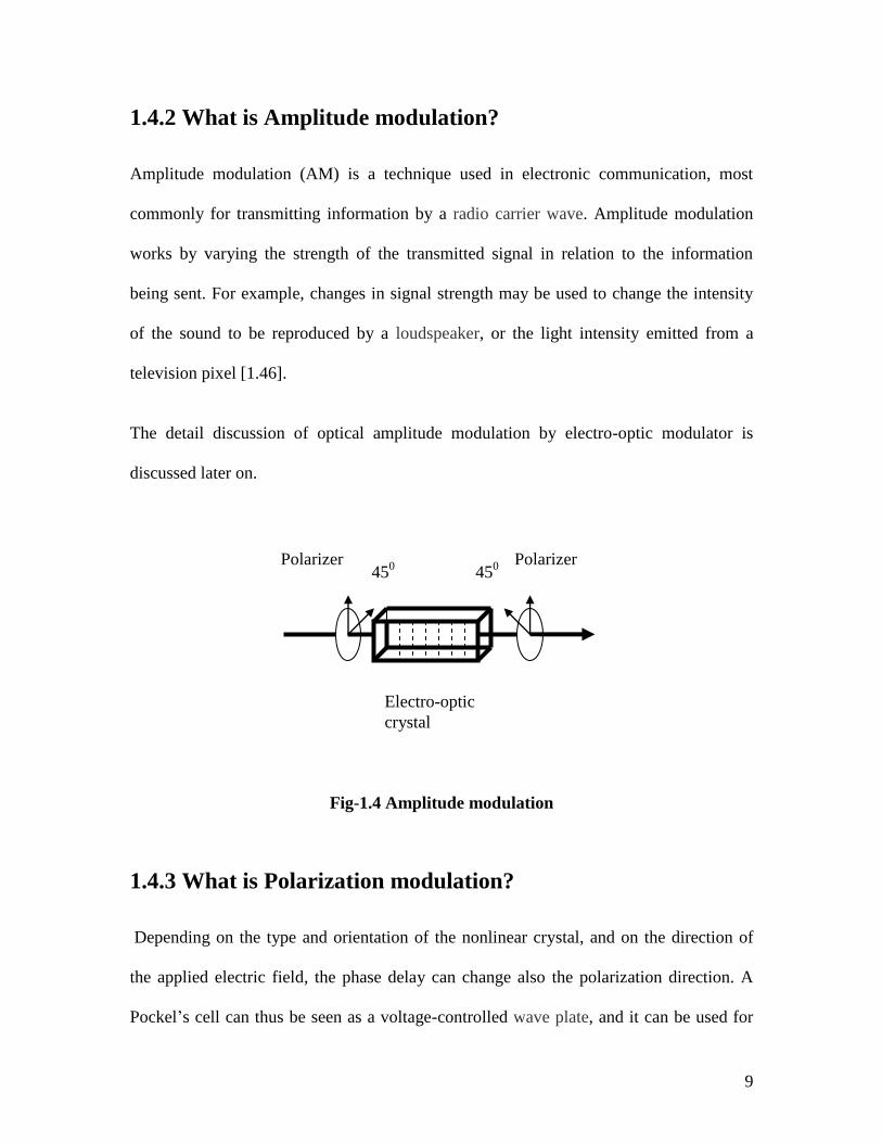
1.4.2 What is Amplitude modulation?
Amplitude modulation (AM) is a technique used in electronic communication, most
commonly for transmitting information by a radio carrier wave. Amplitude modulation
works by varying the strength of the transmitted signal in relation to the information
being sent. For example, changes in signal strength may be used to change the intensity
of the sound to be reproduced by a loudspeaker, or the light intensity emitted from a
television pixel [1.46].
The detail discussion of optical amplitude modulation by electro-optic modulator is
discussed later on.
Fig-1.4 Amplitude modulation
1.4.3 What is Polarization modulation?
Depending on the type and orientation of the nonlinear crystal, and on the direction of
the applied electric field, the phase delay can change also the polarization direction. A
Pockel’s cell can thus be seen as a voltage-controlled wave plate, and it can be used for
Electro-optic
crystal
Polarizer Polarizer 45
0 45
0

10
modulating the polarization state of the carrier light in accordance to the variation of
message signal .For a linear input polarization (often oriented at 45° to the crystal axes),
the output polarization will in general be an elliptical one, rather than being simply a
linear polarization state [1.47, 1.48].
1.5. Electro-optic effect in KDP crystal in longitudinal
mode:
First a linearly polarized plane wave (polarized along X direction) is considered which
propagates along the Z-direction in a KDP crystal of length .Now an external electric
field is applied along the same Z-direction and therefore the refractive index of the light
will change accordingly (fig.1.5). The resulting output beam therefore becomes a phase
modulated beam due to Pockel effect of the KDP crystal [1.31]
Fig-1.5 The phase modulation with KDP crystal.
X
Y
z
KDP crystal
V
Z Pass
axis X
polarizer
Modu
lated
out
put
beam
Z
x
Y

11
The refractive index ( xn ) of a KDP crystal for the rays passing through the Z axis and
polarized along the X axis is
)(2
163
3
00 Zx Ernnn (1..9)
Where n0 is a constant refractive index term of KDP, r63 is a material constant of KDP
and EZ is the externally applied electric field in the KDP along Z direction.
Similarly if the beam polarized along Y direction is sent along the Z direction then the
refractive index is
)(2
163
3
00 Zy Ernnn (1.10)
From in equation (1.9) we get
zx Ernnn 63
3
002
1 (1.11)
From this equation one can see that change in refractive index is very small as for KDP
crystal the value of 0n =1.512 and 12
63 105.10 r m/V.
I f the value of the wavelength of the used light beam is 0.5 m for the z direction
propagation of light , applied electric field is 10-6
v/m and length of the crystal is 1cm
then phase change in transverse mode is[
8.0
2 n (1.12)

12
This is a large phase shift. For electro-optic effect in longitudinal mode in KDP crystal
both types of modulations (phase and amplitude modulation) can be observed
successfully.
1.5.1 Phase modulation by KDP crystal:
First we consider a linearly polarized light which is passing along z direction in a KDP
crystal and polarized along x axis. Now the external electric field is applied along the z
direction and we consider principal axis is along xdirection and thus the linearly
polarized light wave will propagate without any change in state of polarization .From the
figure (fig 1.5) we can see that light polarized at 450 to the x axis is passed along the z
direction through the KDP crystal. The resulting out put beam is thus phase modulated.
If we take a crystal of length along the z direction and then the wave emerging from
the crystal will be [1.31, 1.49, and 1.50]
)cos()0()( 0 xxx ntz
})2
()(cos{)0( 63
3
00
zx Erncc
nt
(1.13)
Here c
0 is the free space propagation constant, z=0 is a assumed to be the input face
of the crystal.
The voltage V is applied across the crystal can be expressed as
ZEV (1.14)
If this applied voltage V is oscillatory in nature with the frequency m thus then

13
}sin)2
(cos{)0()( 063
3
000 tVrnc
ntz mxx
(1.15)
Where, 063
3
02
Vrnc
(1.16)
Using Bessel’s function as given below
...................4cos)(22cos)()()sincos( 420 tJtJJt mmm (1.17)
.....................3sin)(2sin)(2)sinsin( 31 tJtJt mmm (1.18)
And substituting the value of the equation (1.16), (1.17),(1.18)in equation ( 1.15)
We get, one can get
..............))2cos{()(})cos{()(
})cos{()()cos()()[0()(
002001
001000
ntJntJ
ntJntJz
mm
mxx (1.19)
Therefore the output beam contains in addition to the fundamental frequency with
amplitude )(0 J , various side bands at frequencies m , m 2 etc. with respective
amplitudes ....).........(),( 21 JJ .respectively. As 0)(0 J when 4048.2 , all the
power in the fundamental frequency is transferred to the respective harmonics.
1.5.2 Amplitude modulation in the KDP crystal:
Amplitude modulation is a technique used in electronic communication, most commonly
for transmitting information via a radio carrier wave.
A linearly polarized wave polarized along the xdirection and traveling along the z
direction in a KDP crystal in which an external electric field ZE is applied along the z
direction and therefore the output wave at z would be given by[1.31,1.46],

14
zxx Erncc
nti 63
3
00 )2
()([exp{)0()(
(1.20)
Now we take another light beam which is polarized along the y direction, is taken and
then the output wave form can be written as
]})([){0exp()0()( c
nti yyy
(1.22)
Or, ]})2
()([exp{)0()( 63
3
00 zyy Erncc
nti
(1.23)
These two light beams are taken from a single light beam polarized at 450 to x and y
at the input of electro-optic crystal.
Now an incident wave polarized along y direction is taken which decomposed into two
linearly polarized waves along the x and y directions these two components will have
equal amplitudes and will be in phase at z=0 now develop a phase difference which is a
function of the applied electric field. The retardation at z between the two
components will be,
Vrnc
Ernc
Z 63
3
063
3)()(
(1.24)
Thus the electro-optic retardation is independent of the length of the crystal and depends
only on the externally applied voltage.
Now we superpose two linearly polarized waves which are polarized along two
perpendicular directions and then we get a resultant wave of an elliptically polarized
nature. For the phase difference of integral multiple of , the superposition leads to a
linearly polarized wave and for phase difference with odd integer of multiples of 2
leads

15
to a circularly polarized wave .The half wave voltage V which introduce a phase shift of
between two polarized components and it can be written as,
Vrn
c63
3
0)( (1.25)
Or,63
3
0
0
2 rnV
(1.26)
Now one can introduce retardation between the components polarized waves along x
and y directions by the application of an external field and the magnitude of the
retardation is directly proportional to the magnitude of the electric field which leads to an
elliptically polarized wave in general. Now passing the electrically polarized beam
through an analyzer oriented perpendicular to the input polarization state and then the
amplitude of the beam emerging from the analyzer will be thus modulated.
Fig 1.6 shows an electro-optic amplitude modulator using KDP. Here input beam along
the y direction, which is at 450 to the x direction and also the analyzer is placed along X
direction. The input unpolarized laser beam is passed through a polarizer oriented with its
pass axis along the y direction. The out put beam is passed through an analyzer with its
pass axis along the X direction.

16
Fig- 1.6 Amplitude modulation of KDP crystal
Emerging light wave from the analyzer is given as,
)(2
1)
4sin()
4cos( yxyxx
(1.27)
The amplitude of the wave polarized along the x and y directions are equal since the
input beam is linearly polarized along the y axis.
Thus2
)0()0(A
yx (1.28)
Putting the values of equations (1.20) and (1.22) in equation (1.27)
We get,
)}exp(1}]{)2
()({exp[2
163
3
00
iErn
cc
ntiA Z
(1.29)
Where, )()( 63
3
0
V
VErn
cz (1.30)
Polarizer
KDP
Analyzer
Pass axis Pass axis
Y Y
X
Amplitude
Modulated
beam Un polarized
Light beam
V

17
Therefore the intensity of the input beam is expressed as,
Vrnc
AAI 63
3
0
2222*
0 )2
{(sin2
1)
2(sin
2
1)Re(
2
1 (1.31)
The intensity of the output beam is given by,
2
2AI i (1.32)
Or, )}(2
1{sin 20
V
V
I
I
i
(1.33)
Now the sinusoidal input voltage is
)cos(0 tVV (1.34)
Thus the relation of output and input intensities (T=transmittance) is,
)}cos()(2
1{sin 020 t
V
V
I
IT
i
(1.35)
If we assume VV 0 then can approximately obtain,
)}2cos(1{8
)(cos4 2
2
02
2
2
2
02
0 tV
Vt
V
V
I
I
i
(1.36)
Indeed, for a weak input signal VV 0 at frequency it leads an output modulated
beam at twice the signal frequency, namely at 2 .Also if VV 0 , the depth of the
modulation8
2
2
0
2
V
V will be very small.
If the applied signal voltage is much lees than the half wave voltage then, the
transmittance
)cos1(2
1)1(
2
1 00 tV
V
V
V
I
IT
i
(1.37)

18
Which shows that the transmitted intensity is linear relied to the applied voltage.
1.5.3 The Eletro-optic effet in KDP crystals in transverse
mode:
For transverse mode the retardation is independent of the length of the crystal and
depends only on the applied voltage which is applied along the direction of propagation
of the beam. In this configuration the beam passes through either a transparent electrodes
or a small aperture at the entrance of the electrodes on the both ends.
The advantages of the configuration are that, the electrodes no longer abstract the optical
beam as in the longitudinal case and as the retardation is proportional to the applied
voltage and also the length of the crystal and thus the half wave voltage is proportional to
the ratio of the width of the crystal to its length. Thus by decreasing this ratio, one can
have lower half wave voltage [1.33].

19
Fig- 1.7 Modulation out put beam in transverse mode
In figure-1.7 we show an Electro-optic KDP modulator in the transverse mode of
operation. Incident light wave is polarized at 450 to the x direction and propagate along
the y direction, the electric field is field is applied along the z direction. The analyzer is
placed in a direction normal to the polarizer. A compensator is introduced before the
analyzer so as to bias the modulator in the linear region of the transmittance versus
applied voltage curve. When the electric field is applied along the z direction, the
refractive indices for a wave propagating along the y direction and polarized along the
x and z direction respectively given by the equation as
ze nn (1.38)
Polarizer
Pass
axis
Analyzer
Pass
axis Input beam
KDP
Modulated
beam
ed
Z
Y
X

20
Thus if the light beam incident on the crystal linearly polarized along 450 to the x
direction then the emergent field components along the x and z directions after
traversing a length of the crystal will be [1.31]
])(2
1)({exp[
2)( 63
3
00 zx Ec
rnc
ntiA
y
(1.39)
}])({exp[2
)( c
ntiA
y ez
(1.40)
The field components along the x and z directions at y =0 are assumed to be
)exp(2
)0( tiA
yx (1.41)
)exp(2
)0( tiA
yz (1.42)
The retardation between the two linearly polarized components when the beam emerged
from the crystal would be
)}(2
1){( 63
3
00c
Ernnn Ze
(1.43)
We know d
VEZ (1.44)
Or, )}(2
1){( 63
3
00cd
Vrnnn e
(1.45)
Where V is the voltage applied across a width d of the crystal.
Therefore the phase shift induced by the external modulation voltage is
Vd
rnc
)(2
163
3
0
(1.46)

21
For this configuration ,we define a half-wave voltage, as the voltage required to
introduce an additional phase shift of .Since the phase shift introduced in the absence of
an external field is ))(( 0c
nn e
,the half-wave voltage is defined as
)}(2
1){())(( 63
3
000cd
Vrnnn
cnn ee
(1.47)
Or, )(63
3
0
0
d
rnV
(1.48)
Thus by choosing a small geometrical factor
dthe half-wave voltage can be reduced.
Eletro-optic modulators based on highly Deuterium based KDP and ADP crystals can
operate on the transverse mode, they may require a low driving voltage.
1.5.4 Eletro-optic effect in Lithium Niobate crystals:
We can also use Lithium Niobate as electro-optic materials. If an external eletric field is
applied on the Lithium Niobate crystal along its optic axis chosen as the z axis then the
refractive indices for a light wave polarized along the crystallographic x, y, z directions
are given by [1.31]
zx Ernnn 13
3
002
1 (1.49)
zy Ernnn 13
3
002
1 (1.50)
zez Ernnn 33
3
02
1 (1.51)
Where 13r and 33r are the electro-optic co-efficient s respectively.

22
Here if the light beam is propagated along the y direction and the incident light is linearly
polarized to the z direction in the x-z plane then the retardation at a distance from the
input plane is
xz nn 0
2
(1.52)
Ze
e Ernrn
nnOr )2
(2
)(2
, 13
3
033
3
0
0
0
(1.53)
Therefore one can get the half-wave voltage as,
)()( 13
3
033
3
0
d
rnrnV
e
(1.54)
Where d is the thickness of the crystal. If the incident light was polarized along the z
direction then by the application of an electric field along z it will lead to phase
modulation of the beam and the output light will still be a polarized one along the z
direction. The phase of the emerging beam will be given by
ze
e Ern
n )2
(2
)(2 33
00
(1.55)
Therefore the voltage required to change the phase of the out put beam will be,
)()
2(
2 33
3
0 dV
rne (1.56)
Or, ))((33
3
0
d
rnV
e
(1.57)
These types of electro-optic modulator will be used for different purposes in my carrying
thesis.

23
1.6 Objectives:
The main objective of this work is to develop some theoretical models achieving some
special types of light propagation through non-linear and electro-optic materials. The
detail theoretical development includes following points.
Effect of using a kerr non-linear material before an electro-optic modulator in case of
intensity/amplitude modulation of light.
Development of a new scheme for increasing the power of the harmonic signals of the
phase modulated outputs by using the electro-optic modulator.
Effect of multi-passing technique of a Guassian beam through the electro-optic
modulator during phase modulation for reduction of the V signal.
Some investigations on the increase of band width of the modulated signal during
multi passing of a beam through the electro-optic modulator.
A proposal of a new scheme for achieving the velocity modulation of a light beam by
an electrical message signal.
Effect of using RSOA (Reflecting semiconductor amplifier) after electro-optic
modulator to find the unknown micro-wave frequency.

24
References
1.1) S.Datta “Electronic analog of the electro-optic modulator” Applied physics
letters volume 56, issue 7 pp 665-667(1990).
1.2) DM Gill, Dc Jacobson “Electro-optic modulators” united states Patent (2001)
Patent No.US,6,172,791 B1.
1.3) Qianfan Xu1,Bradley Schmidt
1, Sameer Pradhan
1 and Michal Lipson
“micrometer- scale silicon electro-optic modulator” Nature 435,325-327(2005)
doi:10.1038/nature 03569.
1.4 ) Yongqiang Shi, Cheng Zheng, Hua Zhang, James H. Bechtel, Larry R. Dalton,
Bruce H. Robinson and William H. Steier “Low9sub-1-volt) Half wave voltage
Polymeric Electro-optic modulators Achieved by controlling chromophor
shape” Science vol.288,no 5463 pp 119-122(2000)
Doi:10.1126/science.288.5463.119.
1.5 ) Andrew B. Gpeytak, carl J. Barrelet, Kat Li and charles M. Lieba
“Semiconductor nanowire laser and waveguide electro-optic modulators”
Applied physics letters vol.87 issue 15(2005) doi:10.10631/1.2089157.
1.6) Jan-Michael Brosi, Christian koos, Lucio, C. Andreani, Michael Waldow,
Jwerg Leuthold, and Wolfgang Freudle “High-speed low voltage electro-optic
modulator with a Polymer-infittrated silicon photonic crystal wave guide” optic
Express, vol 16,issue 6,pp 4177-4191(2008) doi:10.136410E.16004177.

25
1.7) Datong chen, Harold R. Fetterman, Antoochen, William H. Steier, Larry R.
Datton, Wenshen Wang and Yongqian shi “Demonstration of 110 GHZ electro-
optic polymer modulator” Applied physics Letters 70.3335(1997)
doi:10.1063/1.119162 vol.70,issue 25.
1.8) Po Dong,Shirong Liao,Dazeng Feng,Hong Liang,Dawei Z heng,Rashanak S
hafiiha,cheng-chin kung,wei Qian,Guoliang Li,Xuezhe zheng, Ashok N
Krishnamoorthy and Mendi Asqhari “Low VPP ,Ultralow –energy, compact high
speed silicon electro-optic modulator”Optic Express vol.17, issue 25, pp.22484-
22490(2009) doi:10.1364/OE.17022484.
1.9) L.Dalton,A.Harper,A.Ren,F.Wang,G.Todarova,J.Chen,C.Zhang,and M.Lee
“Plymeric Electro-optic modulators from chromophoric design to integrations
with semiconductor very large scale integration electronics and silica fiber
optics” American chemical society 38(1)91999)pp8-33doi:101021/ie 9705970.
1.10) Gill,D.M “Thin-flim channel wave guide electro-optic modulator in epitaxial
BaTio3” vol.71 issue 13 pp 1783-1785 Applied Physics Letters(1997)
doi:10.1063/1.119397.
1.11) Nirmalya Pahari, Debendra Nath Das, S. Mukhopadhyay, “All-optical method
for the addition of binary data by non-linear materials”, Applied Optics, 43(33),
6147-6150(2004).
26
1.12) Abhijit Sinha, S. Mukhopadhyay, “Effect of higher order non-linearity in
frequency variation of self-phase modulation in optical fiber communication”,
Chinese Optics Letters, 2(9), 500-502(2005).
1.13) Abhijit Sinha, Harihar Bhowmik, Puspendu Kuila, S. Mukhopadhyay, “New
method of controlling the power of a Gaussian optical pulse through an electro-
optic modulator and a nonlinear wave guide for generation of solitons”, Optical
Engineering, 44(6), 065003(1 June, 2005).
1.14) Puspendu Kuila, Abhijit Sinha, Harihar bhowmik, S. Mukhopadhyay,
“Theoretical study of using an amplitude modulation scheme with an electro-
optic modulator for generation of the proper power shape function of an optical
soliton pulse in a nonlinear waveguide”, Optical Engineering, 45(4),
045002(2006).
1.15) Q.Xu,J.Shakya,M.Lipson “compact electro-optic modulator in silicon –on-
insulator substrates using cavities with ultra –small modal volumes” Lasers and
Electro-optic society (2006) pp 332-333.
1.16) Edward I,Ackerman “Broad Band Linearization of a Mach-Zehnder Electro-
optic modulator”IEEE Transactions on microwave zheory and Techniques
Vol47, No 12 (1999).
1.17) Xueliang Shi,Shilie Zheng,Hao Chi,Xiaofeng Jin and Xianmin Zhang
“Awideband electro-optic modulator based on long range surface plasmon

27
resonances” Journal of optics vol 13 ,No 12 (2011) doi:10.1088/2040-
8978/13/12/12001.
1.18) Bui,D.T. “Improving the behaviour of an electro-optic modulator by controlling
its temperature” Advanced Technologies for communications pp 125-128
(2009) doi:10.1109/ATC 2009.5349256.
1.19) Jon-Michael Brosi,Christon Koss,Lucio Claudio Andreani,Michael Waldow
,Juerg Leuthold and Wolfgang Freude “High speed low voltage electro-optic
modulator with a polymer infiltrated silicon phptonic crystal wavegude”Optic
Express 4177 Vol.16, No 6(2008).
1.20) Lipson .M “Compact Electro-optic modulators on a silicon chip” Selected
topics in quantum electronics IEEE Journal Vol 12,issue 6 pp 1520-1526
(2006)doi:10.1109/JSTQE.2006.885341.
1.21) K.Preston,S.Manipatruni,A.Gondarenko,Carl.B,Poitras and M.Lipson
“Deposited silicon high speed integrated electro-optic modulator”Optic Express
Vol.17,issue 7,PP 5118-5124(2009).doi:10.1364/OE.17.0051118.
1.22) Becker,R.A “Travelling wave electro-optic modulator with maximum band
width length product”Applied physics letters ,Vol .45,issue 11,PP 1168-
1170(1984)doi:10.1063/1.95091.
1.23) Y.Enami,C.T.Derase,D.Mathine,C.Loychik,C.Greenlee,R.H.Norwood,T.D.Kim,
J, Lu, Y. Tian, A.K.Y. Jen and N. Peyghambarian “Hybrid polymer /sal-gel

28
wave guide modulators with exceptionally large electro-optic coefficients”
Nature Photinics 1,PP 180-185(2007) doi:10.1038/nphoton.2007.25.
1.24) Girton,D.G “20 GHZ electro-optic polymer Mach-Zender modulator” Applied
physics Letters, vol 58,issue 16,PP1730-1732 (1991) doi:10.1063/1.105123.
1.25) Dolfi,D.W “40 GHZ electro-optic modulator with 7.5 V drive
voltage”Electronics Letters ,Vol 24,issue 9 PP 528-529(1988)ISSN 0013-5194.
1.26) Gee,C.M “17GHZ bandwidth electro-optic modulator” Applied physics Letters
,Vol 43,issue 11,PP 998-1000(1983) doi:10.1063/1.94211.
1.27) D.D Hudson,K.W.Halman,R.Jason Jones ,S.T Cundiff,Jun Ye and D.J Jones
“Mode locked fiber laser frequency controlled with an intracavity electro-optic
modulator” Optic Letters,Vol 30,issue 21,PP 2948-2950(2005)
doi:10.1364/OL.3.002948.
1.28) F.Zeng and J.Yao “All optical band pass microwave filter based on an electro-
optic phase modulator” Optic Express ,Vol 12,issue 16,PP3814-3819(2004)
doi:10.1364/OPEX .12003814.
1.29) P.Tang,D.J.Towner,A.L.Meier and B.W.Wessels “Low voltage polymerization-
insensitive,electro-optic modulator based on a polydomain bariumtitanate thin
flim”Applied physics Letters ,vol 85,issue 20,4615(2004)
doi:10.1063/1.1819515(3 pages).

29
1.31) “Optical Electronics” , Ajoy Ghatak , and K.Thyagarajan ,(Cambridge
university press 2002).
1.32) “Optics”, A.N.Matreev, Mir Publishers, Moscow ,First Published (1988).
1.33) R. Maji and S. Mukhopadhyay “A method of reducing the half wave voltage
(V) of an electro-optic modulator by multi passing a light through the
modulator” ,Optik Int.J.Light Electron opt(2011).doi:10.106/ijleo.2011.07.035.
1.34) R.S.Jacobson, K.N.Andersen, P.I.Borel, J.Fagepedersen,
L.H..Frandsen,M.Kristensen, A.V .Lavrinenko, G.Moulin, H.Ou, C.Peucheret,
B.Zsigri and A.Bjarklev “Strained silicon as a new electro-optic material”
Nature 441,PP 199-202 doi:10.1038/nature 04706(2006).
1.35) Poloczi,George .T. “Replica molded electro-optic polymer Mach-Zender
modulator” vol 85,issue 10,PP 1662-1664(2004) doi:10.1063/1.1787944.
1.36) Hyun-Chae song,Min-Cheoloh,She-won Ahn,Willium H.Steier,Harold
R.Fetterman and Cheng Zhang “Flexible low voltage electro-optic polymer
modulators”Applied Physics Letters vol82,issue 25,
doi:101063/1.1586474,4432(2003).
1.37) Wang,Q “UWB doublet generation using nonlinearly biased electro-optic
intensity modulator”Electronics Letters,vol 42,issue 22
doi:10.1049/el:20062134 PP1304-1305(2006).
1.38) S.Fu Nanyang,J.Li,P.Shum “Photonic Ultra wideband monocycle pulse
generation using a single electro-optic modulator” ICAIT 08 proceedings of the

30
2008 international conference on Advanced Infocomm Technology
doi:10.1145/1509315.1509318(2008).
1.39) S.Manipatrani,R.K.Dokania,B.Schmidt,Nicolay ,Sherwood ,Droz,Carl
B.Poitras,Alyssa B.Apsel and M.Lipson “wide temperature range operation of
micrometer scale silicon electro-optic modulators” Optic Letters, vol 33,issue
19,doi:10.1364/OL33.002185 PP2185-2187 (2008).
1.40) Yu-Lung,P-Feng,H su “Birefrigence measurements by an electro-optic
modulator using a new heterodyne scheme”Opt-Eng 41 doi:10.1117/1.1512908
pp 2764(2002).
1.41) T.Tanabe,K.Nishiguchi,Eiichi Kuramochi and M.Notomi “Low power and fast
electro-optic silicon modulator with lateral p-i-n embedded photonic crystal
nanocavity” Optic Express ,vol-17,issue 25, doi:10.1364/OE.17.022505 PP
22505-22513 (2009).
1.42) Qianfan Xu,BradleySchmidt,Sammer Pradhan and Michal Lipson “Micrometer
scale silicon electro-optic modulator”Nature 435, doi:10:1038/nature 03569
PP325-327(2005).
1.43) M.Lee,H.E.Katz ,C.Erben,D.M.Gill,P.Gopalun,J.D.Heber and D.J.Mc Gee
“Broadband modulation of light by using an Electro-optic polymer”Science,vol
298 ,No 5597 PP 140-1403 doi:10.1126/science (2002).
1.44) Mark D.Skeldon “Optical pulse-shaping system based on an electro-optic
modulator driven by an aperture coupled stripline electrical wave form

31
generator”Journal of the optical society of America, vol 19,issue 10,PP 2423-
2426 doi:10.1364/JOSAB.19.002423(2002).
1.45) “An alternative optical method of determining the unknown microwave
frequency by the use of electro-optic materials and semiconductor optical
amplifier”, by Rupali Maji and Sourangshu Mukhopadhyay , Optik international
journal for Light Electron optics vol-122,issue 18 pp 1622-1624 (2011)
doi:10.1016/ijleo.2010.10.013.
1.46) “A New Method of Controlling the Self Focusing Length of a Bulk Non-linear
Material Using Electro-optic Material”, by Rupali Maji and Sourangshu
Mukhopadhyay ,IUP journal of Physics,Vol-iii. No-3, PP-16-24(July2010).
1.47) Hill,R.A. “Corona poling of nonlinear polymer thin films for electro-optic
modulators” Applied Physics Letters vol.65,issue 14 doi:10.1063/1.112899
PP1733-1735 (1994).
1.48) A.Donval,E.Foussaere,R.Hiele and J.Zyss “Polarization insensitive electro-optic
polymer modulator” Journal of Applied Physics vol87,issue
7,doi:10.1063/1.1372333 3258(2000).
1.49) Yariv A. Optical Electronics, Halt Rinehart and Winston,New York (1985).
1.50) Yariv A.and Yeh,P. optical waves in crystals John wiley, New York(1984).
32
CHAPTER II
Some important past researches in the area of Electro-
optic modulators.
Abstract:
In 1976 J Jensen and E. Richard first commercially used the electro-optic modulator
[2.1]. Basically it is an optical device in which a signal-controlled element depicting its
electro-optic effect which is used to modulate a beam of light [2.2, 2.3]. The modulation
may be done in phase, frequency, amplitude or polarization of the modulated beam.
Modulation bandwidths extending into the gigahertz range are possible with use of laser-
controlled systems. A few forms of modulators have been developed by (using Pockels
effect) they are different lumped, traveling wave, zigzag, and wave guide type of electro-
optic modulators. Among them lumped modulator is most suitable to be used for
modulation of frequency<1GHz and the crystal length about 1cm.The first useful electro-
optic modulator was made of Potassium dihydrogen phosphate (KDP) by Billings in
1949.However, this device was not applicable to be used for high frequency operation
.After that several thoughts, ideas and innovative works were proposed by various
scientists and technologists all over the world.
In last few decades we have seen that thousands of works are proposed by various
scientists all over the world to describe the important properties of Electro-optic
modulator in the application area. Though it is not possible to cover all the important
works in this area within a few pages of the chapter, but we are extending an effort to

33
include and to refer some works only in the field of Electro-optic modulator in this
chapter. Many other works are not mentioned here in this chapter, due to limitation of
space but we have great feeling on those important works.
2.1 Introduction:
Since the innovation of electro-optic modulation days several applications of Electro-
optic modulator based communications are proposed. Lots of proposals are published
around the world in connection to those works. Several researchers are working on
Electro-optic modulator to enrich the optical communication system.
In this chapter we have discussed some important points from those different proposals
and also we have discussed here about the aims of my proposed Ph.D work.
2.2 Background study of the function of electro-optic
modulator:
In previous many researcher have been worked on electro-optic modulation. There are
several work has been done by international and also national researcher. J Jensen and E.
Richard first commercially invented the electro-optic modulator(1976)[2.1].Lithium
Niobate (Li NbO3),Lithium tantalite(LiTaO3) and Ammonium di hydrogen
phosphate(ADP) are few more capable materials used for light
modulation(Schawlow,1969)[2.5].In 1967,Kaminow and his group constructed light
intensity modulator which has of slight advantage compared to the LiTaO3 due to the
larger electro-optic coefficient of Li NbO3[2.6].Light modulation by using Pockels effect

34
Li NbO3,KDP and ADP was well established (White and Chin,1972;Salvestrini et
al,2004)[2.7].
A few forms of modulation have been developed by using Pockels effect. They are
lumped, traveling wave, Zigzag and optical waveguide modulator. The configuration of
each type of modulator has been described by Chen (1970)[2.8].Among them, lumped
modulator is most suitable to be used for modulation of frequency<1 GHz and with the
crystal length about 1cm.Travelling wave and zigzag modulator are used for modulation
of frequencies greater than 1GHz(Denton et al,1967)[2.9].The type of modulator chosen
depends on the required driving power and crystal length(Chen,1970)[2.8].
A lumped electro-optic optical modulator has been developed by using single crystal
LiTaO3 which is in a cylinder form. A transistor driver amplifier with a 0.2 W output
power is used to drive LiTaO3 at a light wavelength of 6328nm.In order to reduce the
voltage for modulation; the modulator is configured in the transverse mode. The
modulator provides 40% intensity of modulation (Kaminow and Sharpless, 1967)[2.10].
The modulation of light wave is to control variation of detectable properties of the light
wave, such as its intensity (amplitude), phase, wavelength (frequency) or polarization. A
modulator is a device that alters a detectable property of a light wave corresponding to an
applied electric signal. Electro-optic effect is widely used for light modulation as it
provides the fastest modulation (Schawlow, 1969, Booth and Hill, 1998)[2.11]. For
electro-optic effect, the application of an electric field across certain crystal is used to
result in change of refractive index of the crystal. The crystal becomes birefringent under
the influence of the applied electric field (O’Konski, 1978;Noriah

35
Bidin,2003)[2.12].These crystal includes Potassium dihydrogen phosphate, Potassium
dideuteriam phosphate, Lithium Niobate, Lithium tantalite and Cesium dihydrogen
arsenate.
The electro-optic effect can be used to control the intensity or phase of the propagating
light (Yariv, 1997)[2.13].The modulation by using electro-optic effect are the basic items
for the optical modulation, optical-switching, Q-switching, and deflection.
The accurate and direct determination of the phase retardation due to the birefringence of
certain materials can be done by using a technique based on the linear variation of the
transmitted intensity with the applied electric field amplitude
modulator(O’Shea,1985)[2.14].High-speed optical intensity modulation is reported for
the first time using single mode interferometer waveguide modulators formed from Ti-
diffused waveguide in LiNbO3(F.J.Leonberger,1980)[2.15].In (1981) V.Hoek and
A.Visser,A.J.W.G worked on Pulse selection system with electro-optic modulators
applied to mode locked CW lasers and time resolved single photon counting[2.16] .The
drive frequency applied to the electrodes structure is used examples of such modulators
are found in Alferness et al, Velocity Matching Techniques for integrated optic Traveling
wave switch/Modulators[2.17], Nazarathy et al, “Spread spectrum Frequency-Response
of coded Phase Reversal Traveling wave modulators”[2.18], and Schmidt, “Integrated
optics switches and modulators”[2.19]. Lithium niobate have seen for many years as
highly functional components for applications in fields such as optical communications
and sensor systems so Lithium niobate used in integrated optics (M.Lawrence,
1993)[2.20].In (1991) Chen et all described about Frequency multiplying electro-optic

36
modulator configuration and method[2.21].In 1994 Gary.E.Betts develops standardized
measures of linearized modulator performance, and uses them to evaluate the
modulator[2.22]. In 1999 shih-jung and at all they developed with the assistance of the
ridge structure, the drive voltage of the of the modulator is reduced by using electro-
optic modulator[2.23]. In 2003 Byungje Lee and et al experimentally shows with the help
of electro-optic modulator 3D finite difference time domain (FDTD) method and 2D
quasi-static formulation have been used to calculate the characteristic impedance and the
microwave effective refractive index of coplanar wave guide on lithium niobate
(LiNbO3) single crystal substrates with a Yttria stabilized Zirconia (YSZ) or SiO2 buffer
layer[2.24].In (2003) Song et all worked on Flexible low-voltage electro-optic polymer
modulators[2.25] .Also in 2003 P. J. Lee and et al demonstrates Atomic qubit
manipulations with the help of electro-optic modulator[2.26]. Yang et al, investigated the
photo-refractive properties of Lithium niobate crystals doped with Manganese(Mn), and
it is found that the effect of dark decay due to electron tunneling which is the limiting
factor of the highest practical doping level, is less in LiNbO3:Mn than in Li NbO3:Fe
(2003)[2.27].In (2005) A.Sinha et al worked on all optical switching
operation[2.28,2.29,2.30,2.31].A ridge type Mach-Zehnder modulator on X-cut Li NbO3
is fabricated by wet etching with proton exchange pretreatment(chang et al,1999).In
(1999) Atlas et all worked on Linearization enhanced operation of single stage and dual
stage electro-optic modulators[2.32]. In (2005) Montgomery et all developed High-speed
silicon based electro-optic modulator[2.33]. Li NbO3 based integrated electro-optic
modulators used in micro-structuring techniques such as etching, domain inversion and
thin film processing(D.Janner et al,2007)[2.34].C.Mok et al., discussed design

37
considerations and construction of a home-built electro-optic phase modulator that can be
used for locking a laser to an atomic transition.(2006)[2.35].Using the micromachining
approach, Yang qiang Shi et al demonstrated significantly reduced resonant mode
coupling loss in LiNbO3 modulators electrodes(2006)[2.36].Electro-optic silicon based
modulator with a bandwidth of 78 GHZ, a drive voltage amplitude of 1 V and a length of
only 80m allows 100Gbit/s transmission and exploits the combination of several
physical effects proposed by Michael et al (2008)[2.37].Microwave and optical properties
of Lithium Niobate electro-optic modulators are investigated by S.Haxha et
al,(2009)[2.38] Kazuto Noguchi demonstrated ultra-high-speed optical modulators
fabricated on LiNbO3 substrate, which are used in large-capacity optical transmission
systems(2007)[2.39].Comparing with one of non-embed end rectangle micro strip line
which is the most familiar configuration of polymer modulator, the optical 3 dB
bandwidths of embedded trapezoidal and T type micro strip increase 264% and 339%
respectively under the condition of impedance matching(Liu et al,2006)[2.40]. In 2008
Mattew J. Dichen and et al demonstrates control of the surface plasmon polariton wave
vector in an active metal-dielectric plasmonic interferometer by utilizing electro-optic
barium titanate as the dielectric layer[2.41]. In 2008 Pavel Kolchin and et al demonstrates
how single photons may be modulated so as to produce photon wave functions whose
amplitude and phase are functions of time [2.42]. In 2009 Abd El Naser A. Mohammed
and et al shows electro-optic modulators in the applications of radio-over-fiber
(ROF)[2.43].In frequency stabilization system E.OM also used when a laser radiation is
modulated by an E.O.M , it produces two sidebands of equal amplitude and also in
demodulated technique E.O.M is used, Therefore the frequency can be stabilized by

38
E.O.M .Recent Grahan Reed, F.Y Gardes worked on developments of electro-optical
modulators[2.44]. Now a days many researcher is doing the to study the characteristics of
microwave frequency by using electro-optic modulator. State of art and prospects
regarding semiconductor compact modulators and transmitters for on off keying and
more advanced modulations formats for output bit rates of 100Gb/s (westergren et
al,2009)[2.35].Ultra broadband electro-optic modulator was developed (Shi and
Prather,2010)[2.46],Dual electro-optic modulator polarimeter is also developed(Song et
al,2010)[2.47].Many researchers are still now trying to demonstrate more characters of
electro-optic modulators, and also trying to exploit their switching phenomenon in optical
and electro-optic communication[2.48,2.49,250].
2.3 Outline of my Ph.D thesis:
Chapter1 includes the basic idea about the modulation processes those by and Eletro-
optic modulators.
Chapter 2 includes the previous works done by Electro-optic modulator, and its
applications.
Chapter3 includes by Use of Kerr type of non linear material and Electro-optic modulator
for the controlling of self-focusing length.
Chapter 4 incorporates the proposal of increasing the power of Harmonics signals during
phase modulation by multi rotation techniques.
Chapter 5 includes the reduction of half wave voltage of the modulator by multi-passing
technique of electro-optic modulator.
Chapter 6 does the same of the increasing the maximum frequency shift of phase
modulation by multi rotation technique.

39
Chapter 7 includes velocity modulation of a light signal by electronic message signal is
an electro-optic modulator.
Chapter 8 includes a novel concept of frequency measurement of unknown microwave
frequency with the help of Optical semiconductor amplifier after an Electro-Optic
modulator by use of known microwave.
Chapter 9 describes the general conclusion and future scope of research in this area.
2.4 Conclusion:
Much progress has been made in the last thirty years in developing modulators, but
device are not very satisfactory for many applications. Different applications of electro-
optic materials, optical Kerr type of materials etc. are discussed in this chapter, where the
devices directly used or used with help of some other devices for the purpose of optical
modulation. Still these are found some lacking in the use of the above devices in high
speed communication or in optical communication. The present thesis will give some
light in the application of electro-optic materials and non-linear materials for some better
communication. Different methods proposed by me have different advantage over
conventional practical communication. Here some method increases higher power etc.
The correctional properties of electro-optic modulator are larges used for proposing some
better methods in optical communication.

40
Referrences
2.1) Jensen, Richard E “Electro-Optic Modulator” , Accession Number : ADD002412,
Subject Categories:Laser sand Masers, Optics, 06 Jan (1976).
2..2) Optical Electrnics “Ajoy Ghatak”, “K.Thyagarajan” (Cambridge university press
2002).
2.3) Yariv A.(1985) Optical Electronics, Halt Rinehart and Winston,New York.
2.4) Yariv A.and Yeh,P.(1984) optical waves in crystals Jahn wiley, New York.
2.5) Schawlow, A. L. (1969). Laser and Light. New York: W. H. Freeman And
Company.332-338.
2.6) Kaminow, I. P. and sharpless, W. M. (1967). Performance of LiTaO3 and
LiNbO3 light Modulator at 4 GHz. Applied Optics. Vol. 6: 351-352.
2.7) White, G. and Chin, G. M. (1972). Travelling Wave Electro-optic Modulator.
Opt. Commun. Vol. 5: 374-379.
2.8) Chen, F.S (1970). Modulators for Optical Communications. Proc. IEEE. Vol. 58
(10):90-105.
2.9) Denton, R. T., Chen, F. S. and Ballman, A. A. (1967). Lithium Tantalate Light
Modulators. Applied Physics. Vol.38 (4): 1611-1617.
2.10) Kaminow, I. P. and sharpless, W. M. (1967). Performance of LiTaO3 and
LiNbO3 light Modulator at 4 GHz. Applied Optics. Vol. 6: 351-352.

41
2.11) Booth, K. and Hill, S. (1998). The Essence of Optoelectronics. Singapore:
Prentice Hall. 135-150.
2.12) O’Konski, C. T. (1978). Molecular Electro-optics Part 1 Theory and Methods.
New York: Marcel Dekker Inc. 393.
2.13) Yariv, A (1997). Optical Electronics in Modern Communications. 5th edition.
New York: Oxford Unversity Press. 326-364.
2.14) O’shea, D. C. (1985). Elements of Modern Optical Design. New York: John
Wiley &Sons. 270-298.
2.15) F.J.Leonberger “High-speed operation of LiNbO3 electro-optic interferometric
waveguide modulators”Optics Letters Vol.5,issue 7,PP312-314(1980)
DOI:10.1364/OL.5000312.
2.16) V.Hoek,A.Visser,A.J.W.G “Pulse selection system with electro-optic modulators
applied to mode locked CW lasers and time resolved single photon
counting”Review of scientific instruments vol 52,issue 8 PP 1199-1205
doi:10.1063/1.1136741(1981).
2.17) Alferness et al, “Velocity-Matching Techniques for integrated optic traveling
wave switch/modulators”,IEEE J.Quantum electronics,VolQE 20,No.3(2984),PP-
301-309.
2.18) Nazarathy et al, “Spread spectrum frequency response of coded phase reversal
Travelling wave modulators”, J.Light w.ave Technology,Vol.LT-5,No.10
October 1987,PP1433-1443.

42
2.19) Schmidt, “Integrated optics switches and modulators” Physics and
applications,S.Martelucci and .A.N.Chester(eds) PP181-210,New Work 1981.
2.20) M.Lawerence “Lithium niobate integrated optics reports on progress pf physics
(1993).56363 doi:10.1088.
2.21) Chen et all “Frequency multiplying electro-optic modulator configuration and
method” United states patent no 5,040,865(1991).
2.22) Gary.E.Betts “Linearized modulator for subocatave-Bandpass optical Analog
links” IEEE Transactions on microwave theory and techniques
,Vol.42,No.12(1994).
2.23) Snih-Jung Chang ,Ching-Long Tsai,Yih-Bin Lin, Ju-FengLiu,and Way-seen
Wang “Improved electro-optic modulator with ridge structure in X-cut LiNbO3”
Journal of Light wave Technology ,Vol.17 issue 5 PP-843(1999).
2.24) Byungje Lee,Joonho Byun,Bok-ki kim “Anaysis of coplanar LiNbO3 waveguide
structures applicable to electr-optic modulator with FDTD method” published in
microwave and optical technology letters (2003) Vol.39,PP234-
237.Doi:10.1002/mop.11178.
2.25) Song, Hyun-chae, Oh, Min-cheol, Ahn, She-won, Steier, William H, Fetterman,
Harold R,Zheng and Cheng “Flexible low-voltage electro-optic polymer
modulators”Applied physics Letters,vol 82,issue 25,pp 4432-4434
doi:10.1063/1.1586474(2003).

43
2.26) P. J. Lee, B. B. Blinov, K. Brickman, L. Deslauriers, M. J. Mad sen, R.Miller, D.
L. Moehring, D. Stick, and C. Monroe “Atomic Qubit Manipulations with an
Electro-Optic Modulator”, Optics Letters, vol 28, no 17(2003).
2.27) Yunping Yang and Demetri Psaltis,Marc Luennemann,Dirk Berben,Ulrich
Hartwing,and Karsten Buse “Photorefractive properties of Lithium niobate
crystals doped with Manganese” J.Opt.Soc.Am Vol.20,No.7/July 2003.
2.28) Abhijit Sinha, Harihar Bhowmik, Puspendu Kuila, S. Mukhopadhyay, “New
method of controlling the power of a Gaussian optical pulse through an electro-
optic modulator and a nonlinear wave guide for generation of solitons”, Optical
Engineering, 44(6), 065003(1 June, 2005).
2.29) Shantanu Dhar, S. Mukhopadhyay, “All optical implementation of ASCII by use
of nonlinear material for optical encoding of necessary symbols”, Optical
Engineering 44(6), 065201(1 June, 2005).
2.30) Archan Kumar Das, S. Mukhopadhyay, “All-optical system for wide range
decimal multiplexing”, Indian Journal of Pure and Applied Physics 43, 253-258
(2005)
2.31) Kuladeep Roy Chowdhury, Debduti De, S. Mukhopadhyay, “Parity checking and
generating circuit with nonlinear material in all-optical domain”, Chinese Physics
Letters, 22(6), 1433-1435 (2005).
2.32) Atlas et all “Linearization enhanced operation of single stage and dual stage
electro-optic modulators”United states of patent no 5,963,352(1999).

44
2.33) Montgomery et all “High-speed silicon based electro-optic modulator” United
states patent no U56,845, 198,B2(2005).
2.34) F.Lucchi,D.Janner,M.Belmonte,S.Balsamo,M.Villa,S.Guiurgola,P.Pruneri “Very
low voltage single drive domain inverted LiNbO3 integrated electro-optic
modulator”published optic express(2007)Vol.15,No.17/optic express 10739.
2.35) C.Mok,M.Weel,E.Rotberg,and A.K.Umarakrishna “Design and construction of
an efficient electro-optic modulator for laser spectroscopy” J.Phys 84:775-
786(2006) doi:10.1139/p06-074.
2.36) Yongqiang Shi,Boeing Satellite Syst,Los Angels,CA USA “Micromachanical
wide-band Lithium niobate electro-optic modulators ”Microwave theory and
techniques, IEEE Transactions on Vol.54,issue:2 PP 810-
815,Doi:10.1109/TMTT.2005.863063(2006).
2.37) Jon-Michael Brosi,Christian Koos,Lucio Claudio,Andreani,Michael
Waldow,Juerg Leuthold,and Wollfagang freude “High-speed low voltage electro-
optic modulator with a polymer-infiltrated silicon photonic crystal wave guide”
Optical society of America(2008) Vol.16,No.6/optic express 4177.
2.38) S.Haxha, B.M.A Rahaman and R.J.Langley “Broadband and low-driving-power
LiNbO3 electro-optic modulators” optical and quantum
electronics,Vol.36,No.14,1205-1220.Doi:10.10071511082-004-5933-8.(2009).
2.39) Kazuto Noguchi “Ultra-high-speed LiNbO3 modulators” Journal of optical and
fiber communications research Vol.4, No.1 i-13,Doi: 10.10297-007-0080-
19(2007).

45
2.40) Zilong Liu,Jihai Yu and Daqing Zhu “Design of a new type of electro-optic
polymer wave guide modulator with ultra high band width” International journal
of infrared and millimeter waves Vol.27,No-5,707-724.Doi:10.1007/s 10762-006-
9108-5(2006).
2.41) Matthew J. Dicken, Luke A. Sweatlock, Domenico Pacifici,Henri J. Lezec,
Kaushik Bhattacharya, and Harry A. Atwater “Electrooptic Modulation in Thin
Film Barium Titanate Plasmonic Interferometers” Nano Lett., 2008, 8 (11), 4048-
4052• DOI: 10.1021/nl802981q • Publication Date (Web): 11 October( 2008).
2.42) P.Kolchin,C Belthengady,S.Du,G.Y.Yin and S.E.Harris “Electro-optic
modulation of single photons”Phys.Rev.Lett,vol,1o1,issue 10 doi:10.1103/Phys
Rev Lett.(2008).
2.43) Abd El-Naser,A.Mhommed,M.A.Metawee,Abd Ei-Fattah,A.Saad,Mohammed
and S.F.Tabbour “Recent applications of the electro-optic modulators in radio-
over-fiber” Published on 6th
Int. conference on high capacity optical networks and
enabling technologies,PP148-153(2009).
2.44) D. J. Thomson, F. Y. Gardes, J.-M. Fedeli, S. Zlatanovic, Y. Hu, B. P.-P. Kuo, E.
Myslivets, N. Alic, S. Radic, G. Z. Mashanovich, and G. T. Reed, “50 Gbit/s
silicon optical modulator,” IEEE Photonics Technology Letters, vol. 24, pp. 234-
236, (2012).
2.45) Urban Westergren,Marck Chacinski and Lars Thylen “Compact and efficient
modulators for 100 Gb/s ETDM for telecom and interconnect applications”
46
Applied Physics A:Materials science and Processing Vol.95,No-4,1039-
1044,doi:10.1007/s 00339-009-5113-6.(2009).
2.46) Shouyan Shi and Dennis W.Prather “Ultrabroadband Electro-optic modulator
based on hybrid Silicon-Polymer Dual Slot Waveguide” Advances IN
Optoelectronics(2010) Vl.2011,doi:10.1155/2011/14895.
2.47) Hongxin Song,Xiaoeng Qi,Weiyao Zou,Zhangyi Zhong and Stephen A.Burns
“Dual electro-optic modulator polarimeter based on adaptive optics scanning laser
ophalmoscope” Opt. express(2010) Vol.18,No 21,PP21892-21904.
2.48) Preston,K.Manipatruni,S.Poitras and C.B.Lipson “2.5 Gbps Electro-optic
modulator in deposited silicon”Lasers and Electro-optics(2009),IAN 10859408.
2.49) M.B.Klein “Dielectric waveguide modulators at 95 GHZ using LiNbO3”
international journal of infrared and millimeter waves Vol 3 .No 5,587595, Doi-
10.1007/BF01009722(1982).
2.50) Shengling Deng,Z.Rena Huang and J.F.McDonald “Design of high efficiency
multi-GHZ SiGe HBT electro-optic modulator” Optic express 13425(2009)
Vol.17.No.16.

47
CHAPTER III
New method of controlling the self focusing length of
non-linear kerr material by the use of Electro-optic
materials.
Abstract
Nonlinear optical materials are used for several physical applications. In optical
switching, lens less optical focusing and defocusing these non-linear materials can show
its strong applications. The focal length of a material (if the material is used for self-
focusing) depends on the applied power. Here in this chapter, a method of controlling the
focal length of a nonlinear material based on the joint use of electro-optic material and a
nonlinear crystal is proposed. The focal length of the nonlinear material depends upon the
voltage applied to the electro-optic material. By changing this voltage/or field in the
electro-optic material, the focal length can be varied and this technique can be used as a
focal length controller. A suitable electro-optic material and a nonlinear material can be
used this purpose.
Papers associated with this chapter
1) R. Maji and S. Mukhopadhyay “A New Method of Controlling the Self Focusing
Length of a Bulk Non-linear Material Using Electro-optic Material”, IUP journal of
Physics, Vol-iii. No 3 pp-16-24 (July 2010).
2) R. Maji and S.Mukhopadhyay “A New Method of Controlling the Self Focusing
Length of a Bulk Non-linear Material by the Use of Electro-optic Material” , 16 th
Pachimbanga Bigyan Congress organized by The Univ of Burdwan ( 27-28 Feb 2009).

48
3.1 Introduction:
When the refractive index of a material is depends on the applied electric field linearly is
called Pockel effect and when it depends on the square of the applied field is called Kerr
effect. The Kerr effect also called quadratic electro-optic effect [3.1]. The Kerr effect has
a distinct from the Pockel’s effect as has the induced index change is directly
proportional to the square of the electric field instead of varying linearly with it. This
refractive index variation is responsible for the nonlinear optical effects like self-
focusing, self-phase modulation and modulation instability and is the basis for Kerr-lens
mode locking. There are several applications of Kerr effects in optical switching,
arithmetic and algebraic operations etc. [3.2, 3.3, 3.4, 3.5, 3.6, 3.7, and 3.8].
In the Kerr electro-optic effect, or DC Kerr effect, a slowly varying external electric field
is applied across the sample material. Under the influence of the external signal the
sample birefringent, with different indices of refraction for light polarized parallel or
perpendicular the applied field. The difference in index of refraction,n,(n=n-n0 ,where
n and n0 the refractive indices of the material with and without the applied of the external
electric field respectively) is given by n=KE2, where is the wavelength of the
applied light, K is a material constant, and E is the strength of the electric field. This
difference in index of refraction helps the material to act as a wave plate when the
polarization of light is perpendicular of the applied electric field. If the material is kept
between two ‘crossed’ linear polarizer’s, no light come out when electric field is turned
off, and almost all the light is transmitted for the application of the optimum value of

49
the electric field. A higher value of the Kerr constant allow as a good transmission with a
smaller applied electric field.
In this particular work, the author shows by the use of Kerr material how one can control
the focal length here the focal length of a non-linear material actually controlled by
applied voltage, and the system is behaves like an optical lens.
3.2 Self-focusing and De-focusing of a Gaussian beam
by the use of non-linear material:
Due to a Kerr type of lensing, an intense optical pulse propagating in a non-linear
medium experiences a self-focusing, where the beam diameter is decreased compared to
of a weaker pulse. The physical mechanism is based on a Kerr nonlinearity with positive
2 .In this situation, the higher optical intensities of near to the beam axis, as compared to
the off axis intensity, causes an increased refractive index in the inner part of the beam.
This modified refractive index distribution acts like a focusing lens. The effect,
occurring in the case of a negative 2 nonlinearity, self-defocusing, where a reduced
refractive index is seen on the beam axis.
A Kerr non-linear process which arises in a media exposed to intense electromagnetic
radiation, and which produces a variation of the refractive index n as described by the
formula n=n0+n2I, where n0 and n2 are the linear and non-linear components of the
refractive index respectively, and I is the intensity of the light passing through it. The
intensity distribution is taken spatially Gaussian, and the sign of the non-linear correction
n2 be either positive or negative, for self-focusing and defocusing [1.1, 1.9].

50
If the non-linear correction term n2 is positive then in peripheral region the plane wave
front takes a concave shape in the direction of the beam and is focused at the optical
axis of the medium (Fig-3.1a).On the other hand if the n2 is negative than central part of
the beam goes faster than that of the peripheral region. Consequently, the plane wave
front takes the shape of a convex shape direction of propagation and. Thus it defocused
into the axis (Fig-3.1b).
Fig-3.1
Focusing and defocusing in a non-linear medium.
a)n2<0, b)n2>0
3.3 Electro-optic material as an Amplitude modulator:
Electro-optic modulator is an optical device in which an electrical signals exploiting the
electro-optic effect and is used to modulate a proper beam of light. The modulation may
be used to change the phase, frequency, amplitude, or polarization of the modulated
beam. Modulation bandwidth at the gigahertz range is possible with the use of a laser
based coherent controlled modulators. [3.10,3.11,3.12,3.13,3.14].
Certain materials change their optical properties when they are exposed to an electric
field. This is caused by the forces that distort the positions and orientations of the

51
molecules the material. The electro-optic effect gives the change in the refractive index
from low frequency electric field to high one up to new
range[3.15,3.16,3.17,3.18,3.19,3.20].
Some electric-optic materials are massively used as amplitude modulator such as
Potassium di-deuterium phosphate (KD*P), Beta-barium borate (BBO), also Lithium
niobate (LiNb03),Lithium Tantalite(LiTaO3) and Ammonium dihydrogen phosphate
(NH4H2PO4,ADP) etc. In addition to these there are also some organic types of special
polymer modulators. A schematic diagram of LiNb03 based electro-optic modulator is
shown in the fig 3.2.
Fig-3.2 An electro-optic amplitude modulator using LiNbo3
X Z
Y
X
y
X
Y
X
Y
Polarizer
e Analizer
Unpolarized
beam
LiNbo3
Amplitude
Modulated
beam
V

52
3.4 Gaussian beam:
Gaussian beam has its transverse electric field and intensity distribution which is well
approximated by Gaussian functions. Many lasers emits beams that has a Gaussian
profile, for that reason the laser is said to be operating on the fundamental transverse
mode, or "TEM00 mode" in the laser's optical resonator. When this beam is refracted by a
diffraction-limited lens, a Gaussian beam is transformed into another Gaussian beam
[3.13,3.14].
The beam profile of a Guassian beam is shown in fig 3.3.
Fig-3.3 Profile of a Gaussian beam

53
3.5 An integrated scheme of controlling the self-
focusing length of a bulk non-linear medium by the
use of electro-optic material:
The refractive indices of the electro-optic modulator is [3.9]
Zx rEnnn3
002
1 (3.1)
Zy rEnnn3
002
1 (3.2)
Where ‘r’ is the material material constant. EZ, is the applied field along z direction.
Fig-3.4 Scheme of controlling the focal length of Gaussian beam by use of E-o
modulator and a Kerr type of non-linear material:

54
First a linearly polarized wave polarized along the x-direction and ( x is one of the bi-
axial direction of the Electro-optic material) traveling along the z-direction through
electro-optic material is considered (fig 3.4), We have applied an external electric field
EZ along the Z-direction (C-axis), then the output wave at Z= (where is the length of
the electro-optic material along z ) would be given by
zXX rEnccnti3
00 )2/()/([exp{)0()( (3.3)
Here )(zx and )(zy are the X and Y components of the electric field of the used
light.
In a similar manner, a beam polarized along the Y-direction (whereY is the other bi-
axial direction of Electro-optic modulator) the output wave at Z= will be given by
zyy rEnccnti3
00 )2/()/([exp{)0()( (3.4)
Now consider an incident wave polarized along the y direction is taken then it can be
decomposed into two linearly polarized waves along two orthogonal direction as
X andY as these two components will have equal amplitudes and will be in phase Z=0,
i.e; at the input of the crystal. Thus the two components which were in phase at Z=o now
develop a phase difference which is a function of the applied electric field (EZ).Thus the
retardation at Z= between the two components will be
=(/c)n03r63EZ =n0
3r63V/c (3.5)
Where V=EZ is the voltage applied across the crystal. One can define the ‘half wave’
Voltage V as the voltage required to develop a phase shift of between the two
orthogonal polarization components

55
So, ==(/c)n03r63V . (3.6)
Or V =0/2n03r63
Substituting the values of x’ and y’ given by the equations (1) and (2), the expression of
the total field () becomes
=2
1Aexp{i[t-(n0/c) +(/2c)n0
3r63EZ ]}[1-exp(-i)] (3.7)
Where =(/c)n03r63EZ =(V/V) (3.8)
Thus the intensity of the output beam is given by
I0=2
1Re[*]=
2
1A
2sin
2
2
1
=2
1A
2sin
2[(/2c)n0
3r63V] (3.9)
Where V=EZL is the applied voltage. The intensity of the input beam (Ii) is given by
Ii=2
1A
2 (3.10)
ThusI0/II=sin2(
2
1V/V) (3.11)
I0/Ii is the transmission coefficient of the electro-optic modulator.
If Vis very less than V
The I0/Ii[4
22
2 )(
V
tV ] (3.12)
Again the nonlinear refractive index of the Kerr type crystal is
n=n0+n2I0 (3.13)
Putting the values of I0 from equation (3.12) in equations (3.13)
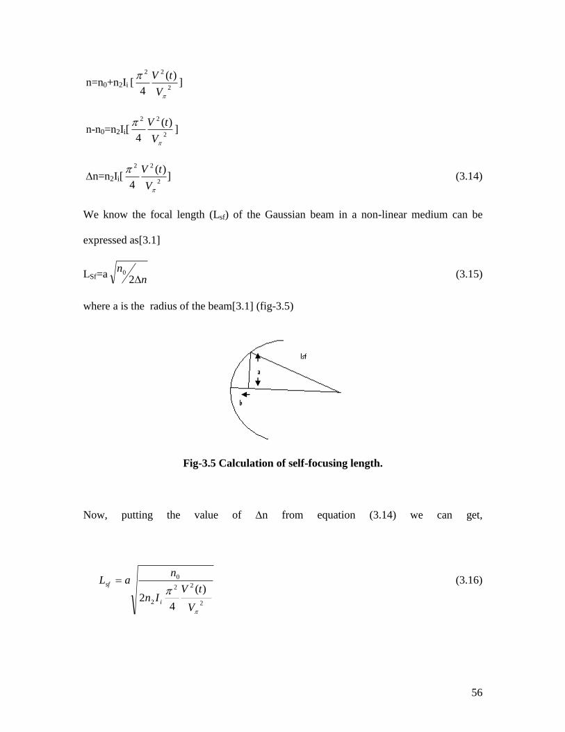
56
n=n0+n2Ii [ 2
22 )(
4
V
tV]
n-n0=n2Ii[ 2
22 )(
4
V
tV]
n=n2Ii[ ])(
4 2
22
V
tV (3.14)
We know the focal length (Lsf) of the Gaussian beam in a non-linear medium can be
expressed as[3.1]
LSf=an
n2
0 (3.15)
where a is the radius of the beam[3.1] (fig-3.5)
Fig-3.5 Calculation of self-focusing length.
Now, putting the value of n from equation (3.14) we can get,
2
22
2
0
)(
42
V
tVIn
naL
i
sf (3.16)

57
It is known that input intensity is Ii , where
Ii=E02 (E0 is the amplitude of the electric field strength of the light at the time of
introduction in the modulator of the axis)
Thus the expression of the focal length can be written as,
Lsf= 2
02
02
)( En
n
tV
aV
(3.17)
2
0
0 2)(
2
n
n
E
a
tV
VLsf
(3.18)
Now E(r) can be written in a radial function (where r is the radial position in the circular
beam)
as E(r) =E0 2
2
1a
r (3.19)
For the mean value of the energy flux density, we obtain the expression
<S>=vE2/2
=[CE0
2/(2n0)](1-r
2/a
2)
=(0n0CE0
2/2)(1-r
2/a
2) (3.20)
The energy flux of the beam is given by
P= rdrarcEndS
a
)/1(.0
222
000
(3.21)
Where is the cross-sectional area of the beam. After integration the total energy flux (P)
can be written as
P=0n0cE02a
2/4 (3.12)

58
E0=can
P
00
2
(3.23)
Thus the self focal length
Lsf=2
000
2
2)( n
n
P
cna
tV
V
(3.24)
3.6 Result:
The result obtained in equation (3.24) can be used to obtain the focal length in Carbon bi
sulphide, or in any other non-linear medium.
For Carbon bisulphide, n0=1.62, n2=0.22*10-19
m2/w
2, thus for a power P=10MW and
beam radius a=1 cm,
( ( the LiNbo3 is used as Electro-optic modulator before the non-linear material) sf
become 6.92m (considering V=64V and V=64v also in equation (3.24))).
Again if the applied voltage V=640V in LiNbO3 the sf becomes 0.692 m.

59
3.7 Conclusion:
From the above analytical treatment it is seen that if an electro-optic Pockel cell is used
before a Kerr-cell which extends the self-focusing then one can easily control the focal
length of the self-focusing system by applying the desired amount of voltage at the
electro-optic material. Similarly the defocusing length can also be controlled by the same
mechanism. The whole scheme may extend a tremendous application in optical
communication through optical fiber. These mechanisms can help the coupling of desired
amount of light intensity in an optical fiber from a source in case of data communication.
To use it in the application domain one can use a suitable electro-optic material and a
suitable simple Kerr non-linear medium.

60
References
3.1) A.N.Matreev,Mir Publishers Moscow First Published (1988).
3.2) P. Kuila,A. Sinha,H.Bhowmik and S.Mukhopadhyay,“Theoretical study of using
an amplitude modulation scheme with an electro-optic modulator for generation
of the proper power shape function of an optical soliton pulse in a non-linear
wave guide,” Opt. Eng. 45(4),920060045 (2002).
3.3) A.Sinha,H.Bhoumik,P.Kuila and S.Mukhopadhyay, “New method of controlling
the power of a Gaussian optical pulse through an electro-optic modulator and a
non-linear wave guide for generation of solitons”,opt.
Eng,44(6)(065003)June(2005).
3.4) P.Mondal and S.Mukhopadhyay, “Analytical study to find the proper coupling
energy from one optical wave guide to another with consideration of the non-
linear correction factor”, opt. Eng (USA),45(11),114605.114602.1-114605.5
(2006).
3.5) P.Mondal and S.Mukhopadhyay, “method of conducting an optical NAND logic
operation controlled from a long distance,” opt. Eng (USA),46(3),.035009 (2006).
3.6) P. Kuila,A. Sinha,S.Mukhopadhyay, “A Theoretical approach for generation of
optical soliton pulse inside an optical fiber using electro-optic modulator”,
accepted for publication in journal of optics (2008).

61
3.7) Cusack,J.Benedict,S.Benjamin,Shaddock,A.Daniel,Gray,B.Malcolm,Lam,Koy
Ping,Whitecomb,E.Stan, “Electro-optic Modulator capable of Generating
Simultaneous Amplitude and Phase Modulations”,Appl.opt.Vol.43(26),5079-
5091 (2004).
3.8) J.Nees,S.Williumson,G.Mourou, “100 GHz traveling wave electro-optic phase
modulator”,Appl.Phy.Lett,Vol.54,1962-1964 (1989).
3.9) “Optical electronics” A.Ghatak, K.Thayagarajan (Cambridge university press
2002.).
3.10) Abhijit Sinha,, and S. Mukhopadhyay, “Effect of higher order non-linearity in
frequency variation of self-phase modulation in optical fiber communication”,
Chinese Optics Letters, 2(9), 500-502(2005).
3.11) G. Fibich and Alexander L. Gaeta “Critical power for self-focusing in bulk media
and in hollow waveguides” Optics Letters, Vol. 25, Issue 5, pp. 335-337 (2000)
doi.org/10.1364/OL.25.000335
3.12) D.Huang, M.lman, Lucio H. Acioli, H.A. Haus, and J.G. Fujimoto “Self-focusing-
induced saturable loss for laser mode locking” Optics Letters, Vol. 17, Issue 7,
pp. 511-513 (1992).doi. org/ 10.1364/ OL.17.000511
3.13) Abhijit Sinha, Harihar Bhowmik, Puspendu Kuila, and S. Mukhopadhyay, “New
method of controlling the power of a Gaussian optical pulse through an electro-
optic modulator and a nonlinear wave guide for generation of solitons”, Optical
Engineering, 44(6), 065003(1 June, 2005).

62
3.14) Puspendu Kuila, Abhijit Sinha, S. Mukhopadhyay, “An all-optical method of
conducting some logic operations by interaction of two modulated Gaussian
pulses,” Journal of Optics, 35(4), 196-205 (2006).
3.15) Sidney A. “Self focusing of spherical Gaussian beams” Applied optics / Vol. 22,
No. 5 / 1 March 1983.
3.16) A. Bencheikh, M. Bouafia, K. Ferria “new spherical aberration coefficient C4 for
the Gaussian laser beam” Optica Applicata, Vol. XLI, No. 4, 2011.
3.17) Gee, C.M “17GHZ band width electro-optic modulator” Applied physics Letters,
Vol 43, issue 11,PP 998-1000(1983)doi:10.1063/1.94211.
3.18) Girton, D.G “20GHZ electro-optic polymer Mach-Zehnder modulator ”Applied
physics letters, vol 58,issue 16 pp 1730-1732 (1991) doi:10.1063/1.105123.
3.19) Spickermann. R “GaAS/AlGaAs traveling wave electro-optic modulator with an
electrical bandwidth >40GHZ”Electronics Letters.vol 32, issue 12,pp 1095-1096
(1996) doi:10.1049/el.1966745.
3.20) Miller, D.A.B “Novel hybrid optically bi stable switch the quantum well self
electro-optic effect device” Applied physics letters , vol 45,issue 1 pp 13-15
(1984) doi: 10.1063/1.94985.

63
CHAPTER IV
Method of Increasing the Power of the Harmonics in
Optical Phase Modulation by Electro-Optic Material
Abstract:
Electro-optic material has several applications in optical communication, integrated
optics and data processing. The modulator is generally used for the purpose of amplitude
and phase modulation of a light signal by the use of an electrical message signal. In this
chapter I propose a new and alternative method of an electro-optic modulation where the
power level and intensities of the output harmonic signal except that of the central carrier,
can be increased in case of phase modulation of a LiNbo3 based electro-optic modulator,
if multi passing technique of the optical signal through the electro-optic material is
applied.
Papers associated with this chapter
1) R. Maji and S. Biswas S. Mukhopadhyay “An optical method of increasing the
maximum frequency shift in phase modulation by electro-optic crystal with multi passing
technique”, communicated to ‘Chinese Optics Letters.
2) R. Maji and S. Mukhopadhyay “A method of increasing the power of the harmonic signals
of the phase modulated output from an electro-optic modulator”, second National seminer on
recent trends in condensed matter Physics including laser application organized by The
department of Physics Univ of Burdwan (SNSCMPLA 22-23March 2012).
3) R. Maji and S. Biswas S. Mukhopadhyay “New method of changing the power of
the harmonics of phase modulated optical signal by using multi-passing technique in
electro-optic crystal” , in the XXXVII National symposium of Optical society India in
the University of Pondicherry on 21st Jan 23
rd Jan (2013).

64
4.1 Introduction:
Phase modulation is a method of impressing data onto an alternating current waveform
by varying the instantaneous phase of the wave. This scheme can be used with analog or
digital data. An electro-optic modulator is a device which is used for controlling the
power, phase or polarization of a laser beam with an electrical control signal. The
principle of operation is based on the linear electro-optic effect, i.e, the modulation of the
refractive index of a nonlinear electro-optic crystal by an applied electrical
field[4.1,4.2,4.3,4.4,4.5,4.6].This refractive index sometimes is linearly proportional with
the electric field in case of Pockel’s type of electro-optic crystal like KDP, ADP, LiNbO3
etc [4.7,4.8,4.9,4.10,4.11,4.12]. This material are massively used as amplitude modulator,
phase modulator, optical shutter etc because of the above electrical behavior [4.13, 4.14,
4.15, 4.16, 4.17, 4.18, 4.19]. It was already reported by the group of authors that if multi
passing scheme is used the V voltage of an elector-optic modulator can be reduced,
which can give a potential use in optical modulation. In this paper report an alternative
analytical observation that if the above multi passing technique is used for phase
modulation in electro-optic modulator, the power level or the intensity level can be
increased in the out put harmonics a the cost of reduction of the power level in the
central frequency of the used light.

65
4.2 Phase modulation by electro-optic modulator:
Phase is a type of electronic modulation in which the phase of a carrier wave is a varied
in order to transmit the information contained in the signal. Phase modulator is used. In
communication systems, in which the phase of the radio carrier wave is varied in order to
transmit the information contained in the signal. Phase changes the phase angle of the
complex envelope in direct proportion to the message signal. Suppose that the signal to
be sent is m(t) and the carrier onto which the signal is to be modulated is
)sin()( ccc tAtc .This makes the modulated signal ))(sin()( ccc tmtAty .In
analog phase modulation the A.C signal wave, also called the carrier ,varies in a
continuous manner. Thus, there are infinitely may possible carrier states, when the
instantaneous data input wave form has positive polarity, the carrier phase shifts in one
direction, when the instantaneous data input wave form has negative polarity, the carrier
phase shifts in the opposite direction. At very instant in time, the extent of carrier phase is
directly proportional to the extent to which the signal amplitude is positive or negative
( fig-4.1).
Fig-4.1Phase modulation
Polarizer
Electro-optic
modulator Oscillator
Polarizer
optional
Phase
modulated
out put
beam
Input
beam

66
4.3 Analytical treatment of getting higher intensity of
the harmonics of the phase modulated output from
an electro-optic modulator by multi-passing
technique of the carrier light:
Here a LiNbO3 or KDP electro-optic modulator is connected with an externally applied
electrical potential difference V, along its Z-axis which is its optic axis (fig-4.2).The
length of the modulator is along its z axis. Now a polarized light wave passing through
the electro-optic modulator. After passing the electro-optic modulator the expression of
the electrical-field is
Fig-4.2 A schematic diagram of increasing power of the harmonic signal (Mi
i=1,2,3,4 mirror)
V
d
Electro-optic
modulator
S M4
d1
M1
M2
M3
x
z Compensator
y

67
0cos011
xXX ntZE
163
3
002
cos01
ZxErn
ccnt
=
1063
3
000 sin2
cos01
tvrnc
nt mX (4.1)
Thus after completion of a cycle i.e after its 2nd
time passing through the modulator the
light gets its electric field as,
2063001063
3
000 )sin(sin2
cos022
ommXX ktvrnntvrnc
ntE
=
21063
3
000 sin2
22cos02
tvrnc
nt mx (4.2)
From eqn(1)
063
3
012
vrnc
(4.3)
From eqn (2)
063
3
022
2 vrnc
(4.4)
The eqn.2 can be written as
21063
3
000063
3
000 sin2
sin2
cos022
tvrnc
ntvrnc
ntZE mmxX

68
})cos{()0()( 122
tntZE mXX ,n1=0,1,2… (4.5)
Similarly after completion of n-cycle one can get,
})cos{()0()( 1 tntZE mxX nn
(4.6)
The amplitude of the harmonic signals after n time passing through the electro-optic
modulator is
)()0(........),........()0(),()0(),()0( 210 nnxnXnxn jEjEjEJEnnnnX
.
nvrnc
nn
063
3
02
(4.7)
Where n=1,2,3 ------------------------------------
4.4 Result:
For KDP crystal the value of vrnc
nn 63
3
0)2
(
where n=1,2,3…………….
Here 1510 Hz, ,512.10 n 12
63 105.10 r , 1000 v Volt, 8103c m.
The analytical result of variation of n vs. Jn2 for KDP crystal is given in Table 1.

69
Table 4.1 n vs Jn2 for KDP crystal
n J02
J12
J22
J32
J42
J52
0.00265 1 1.7503310-6
7.6591210-13
1.4895510-19
1.6295110-26
1.1408710-33
0.00529 0.99999 7.0012710-6
1.2254510-11
9.5331210-18
4.1715310-24
1.1682510-30
0.00794 0.99997 1.5752710-5
6.2038310-11
1.0858810-16
1.0691110-22
6.7366810-29
0.01058 0.99994 2.8004510-5
1.960710-10
6.1011310-16
1.067910-21
1.1962810-27
0.01323 0.99991 4.3756310-5
4.7868210-10
2.3273810-15
6.3651510-21
1.1141110-26
0.01588 0.99987 6.3007910-5
9.9258110-10
6.9494510-15
2.7368810-20
6.8982610-26
0.01852 0.99983 8.5758810-5
1.8388510-9
1.7523710-14
9.3934610-20
3.2225810-25
0.02117 0.99978 1.1200910-4
3.1369410-9
3.9045610-14
2.7337410-19
1.2249510-24
0.02381 0.99972 1.417510-4
5.0246810-9
7.9155510-14
7.014110-19
3.9777810-24
0.02646 0.99965 1.7500210-4
7.6582410-9
1.4894210-14
1.6293910-18
1.140810-23
Now the variation of J02 vs n (n is the number of times of passing the light through the
modulator).The variation of 2
0J (2
0J is the intensity of the central frequency of the
light) with n is show in figure 2.It is seen that the intensity of the central frequency
decrease with number of passing the light. In fig 3,fig 4,fig 5,fig 6,fig7 the variation
of 2
6
2
5
2
4
2
3
2
2 )(,)(,)(,)(,)( nnnnn JJJJJ respectively with n1 are shown. It can

70
be seen in all case that the power of the harmonic signals increases with n, the number of
passing the light through the modulator, whereas the power of the central frequency
decreases with n,
Plot tings Jn2 vs.
1n (i.e. n1 ζ) for KDP crystal where n=1, 2, 3
………harmonics and n1=1, 2, 3…..no. of times passing through Modulator.
Plot tings 1n vs Jn
2 for KDP crystal where n=1,2,3 ………
Fig-4.3Variation of 2
0 )( nJ vs n
Fig-4.4Variation of 2
1 )( nJ vs n

71
Fig-4.5Variation of 2
2 )( nJ vs n
Fig-4.6Variation of 2
3 )( nJ vs n

72
Fig-4.7Variation of 2
4 )( nJ vs n
Fig-4.8 Variation of 2
5 )( nJ vs n

73
4.5 Analytical finding of the variation of harmonic
power with the number of passing of the light
through the modulator during the phase
modulation of the light through the LiNbO3 crystal.
Table:4.2 n vs Jn2 for LiNbO3 crystal
n J02
J12
J22
J32
J42
J52
0.00329 0.99999 2.7099110-6
1.8359110-12
5.5279810-19
9.3627310-26
1.0148910-32
0.00658 0.99998 1.0839610-5
2.9374410-11
3.5378910-17
2.3968510-23
1.0392410-29
0.00988 0.99995 2.4388710-5
1.4870710-10
4.0298510-16
6.1428410-22
5.9927810-28
0.01317 0.99991 4.3356810-5
4.6998110-10
2.2642110-15
6.1358610-21
1.0641810-26
0.01646 0.99986 6.7743410-5
1.147410-9
8.6371810-15
3.6572210-20
6.1360610-25
0.01975 0.9998 9.7547610-5
2.3791910-9
2.5790110-14
1.5725210-19
6.1364610-24
0.02305 0.99973 1.3276810-4
4.4076410-9
6.5031810-14
5.3971510-19
2.8666910-24
0.02634 0.99965 1.7340510-4
7.5190410-9
1.44910-13
1.570710-18
1.0896710-23
0.02963 0.099956 2.194510-4
1.2043710-8
2.9374710-13
4.0310-18
3.5384510-23
0.03292 0.99946 2.7091910-4
1.835510-8
5.5272310-13
9.3617310-18
1.014810-22
Now the analytically obtained result of variation of central frequency and harmonic
signals with number of passing through LiNbO3 is shown in Table 2.
The analytical result of Variation of 2)( nnJ vs n in case of LiNbO3 .
Now instead of taking KDP if LiNbO3 is taken as modulator some time of analytical
results are found out. In Table 2 we have shown the value of 2)( nnJ vs n n, and with

74
the results the nature of the variation of 2)( nnJ vs n are shown in the fig 8,fig,9,fig
10,fig 11,fig12.
Plot tings 1n vs Jn
2 for LiNbO3 crystal where n=1,2,3 ………
Fig-4.9Variation of 2
0 )( nJ vs n
Fig-4.10Variation of 2
1 )( nJ vs n
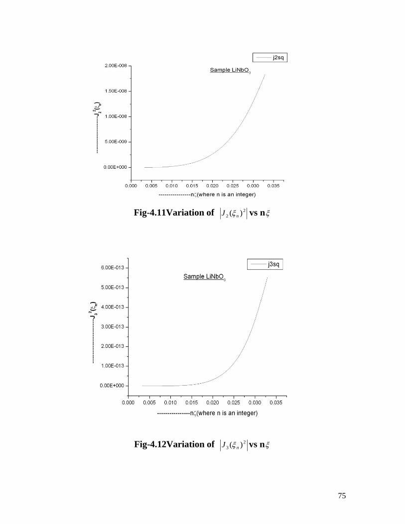
75
Fig-4.11Variation of 2
2 )( nJ vs n
Fig-4.12Variation of 2
3 )( nJ vs n

76
4.6 Conclusion:
In this chapter I have shown the nature of variation of intensity /power of the harmonic
signals obtained at the output of the electro-optic modulator, which depends on the
number of passing of radiation through the modulator .In each case (in case of KDP &
LiNbO3 )it is observed that the power of the central carrier frequency 2
0 )( nJ falls with
the number of passing n of the radiation, where as the power of the harmonic signals
2
1 )( nJ increases with number of passing of the radiation through the modulator. Thus
the propose scheme will be beneficial for increasing the harmonic power of the radiation
passing through the electro-optic modulator by multi-passing mechanism. Generally the
power of the central frequency is wastage at the time of phase/frequency modulation,
where powers of the harmonics are important for practical application. In the present
scenario one can increase the harmonic power making the power of central frequency
decreased.
In the curves it is seen that the power of harmonic light signal is increasing where as the
same in central frequency decreasing. From this work one can conclude that by multi-
passing of the beam one can increase the power of the harmonics of the phase modulated
output.

77
References
4.1) Optical Electrnics “Ajoy Ghatak”, “K.Thyagarajan”(Cambridge university press
2002).
4.2) Yariv A.Optical Electronics, Halt Rinehart and Winston,New York. (1985)
4.3) Yariv A.and Yeh,P. optical waves in crystals Jahn wiley, New York .(1984).
4.4) J. Niedziela “Bessel Functions and Their Applications” University of Tennessee
Knoxville( 2008).
4.5) S. Mukhopadhyay, D. Das, P. Das, P. Ghosh, “Implementation of all-optical
digital matrix multiplication scheme with non-linear material”, Optical
Engineering, 40(9), 1998-2002(1 September, 2001).
4.6) K. Roy Chowdhury, S. Mukhopadhyay, “Binary optical arithmetic operation
scheme with tree architecture by proper accommodation of optical nonlinear
materials,” Optical Engineering, 43(1), 132-136(1 January, 2004).
4.7) N. Pahari, S. Mukhopadhyay, “New method of all-optical data comparison with
nonlinear material using 1’s complement method”, Optical Engineering, 45(1),
015201(2006).
4.8) S. Dhar, S. Mukhopadhyay, “All optical implementation of ASCII by use of
nonlinear material for optical encoding of necessary symbols”, Optical
Engineering, 44(6), 065201(1 June, 2005).

78
4.9) Prasanta Mondal and S. Mukhopadhyay, “Analytical study to find the proper
coupling energy from one optical waveguide to another with consideration of the
nonlinear correction factor”, Optical Engineering (USA), 45(11), 114602.1-
114602.5(2006).
4.10) F.Lucchi,D.Janner,M.Belmonte,S.Balsamo,M.Villa and S.Guiurgola,P.Pruneri
“Very low voltage single drive domain inverted LiNbO3 integrated electro-optic
modulator” published optic expressVol.15,No.17/optic express 10739(2007).
4.11) P.,K.Manipatruni,S.Poitras and C.B.Lipson “2.5 Gbps Electro-optic modulator in
deposited silicon” Lasers and Electro-optics,IAN 10859408.(2009).
4.12) S. Deng,Z.Rena Huang and J.F.McDonald “Design of high efficiency multi-GHZ
SiGe HBT electro-optic modulator” Optic express 13425Vol.17.No.16. (2009)..
4.13) Y. Shi,Boeing and C.A “Micromachanical wide-band Lithium niobate electro-
optic modulators” Microwave theory and techniques, IEEE Transactions on
Vol.54,issue:2 PP 810-815,Doi:10.1109/TMTT.2005.863063(2006).
4.14) S.Haxha, B.M.A Rahaman and R.J.Langley “Broadband and low-driving-power
LiNbO3 electro-optic modulators” optical and quantum electronics, Vol.36,
No.14,1205-1220.Doi:10.10071511082-004-5933-8.(2009).
4.15) Zilong Liu,Jihai Yu and Daqing Zhu “Design of a new type of electro-optic
polymer wave guide modulator with ultra high band width” International journal
of infrared and millimeter waves Vol.27,No-5,707-724.Doi:10.1007/s 10762-006-
9108-5(2006).

79
4.16) S. Shi and Dennis W.Prather “Ultrabroadband Electro-optic modulator based on
hybrid Silicon-Polymer Dual Slot Waveguide”Advances IN
OptoelectronicsVl.2011, doi:10.1155/2011/14895(2010).
4.17) R. Maji and S. Mukhopadhyay “An alternative optical method of determining the
unknown microwave frequency by the use of electro-optic materials and
semiconductor optical amplifier” ,Optik Int,j.Light Electron,vol ,issue pp (2011).
4.18) R. Maji and S. Mukhopadhyay “A method of reducing the half wave voltage (V)
of an electro-optic modulator by multi passing a light through the modulator”
,Optik Int.J.Light Electron vol ,issue pp.(2012).
4.19) R. Maji and S. Mukhopadhyay “A New Method of Controlling the Self
Focusing Length of a Bulk Non-linear Material using Electro-optic Material” ,
IUP journalof Physics,Vol-iii. No 3 pp-16-24 (July 2010).

80
CHAPTER V
Optical Method of Reduction of the Half-Wave Voltage
V of an Electro-Optic Modulator by Multi-Passing
Technique
Abstract:
Electro-optic material has multifaceted applications in optical communication as well as
in integrated optics. Mainly in case of optical modulation of an electrical message signal
modulates a carrier light wave it can show its importance. The V voltage of an electro-
optic modulator is an important parameter for the modulation. The increase of V is
related with the increase of power requirement for modulation. Here in this chapter a
method of reduction of V voltage by multi-passing of the beam through the modulator is
proposed.
Papers associated with this chapter
1. R. Maji and S. Mukhopadhyay “A method of reducing the half wave voltage(V) of
an electro-optic modulator by multi passing a light through the modulator” ,. Optik Int.
Journal for .Light Electron optics vol-123, issue12 ,pp-1079-
1081(2012).doi:10.106/ijleo.2011.07.035.

81
5.1 Introduction:
A commonly used parameter of merit for electro-optic modulators is the half-wave
voltage; V .It is defined as the voltage required producing a phase shift of 1800 in a light
beam passing into the modulator. There are many applications of electro-optic Pockels
cell in Q- switching.
One of the important properties of Pockels cell is the half-wave voltage V.In an
amplitude modulation scheme [5.1, 5.2, 5.3, 5.4, 5.5, 5.6, and 5.7], the applied voltage is
to be changed by the value of V to go from minimum transmission to that with
maximum transmission. The half-wave voltage of a Pockel’s cell in a transverse electric
field depends on the crystal material; the electrode separation and the length of the region
where electric field is applied. For a Pockel cell applied in longitudinal electric field, the
crystal length is not a factor. So V voltage plays a significant role in Pockeles cell, as
more V voltage requires more strength of the message signal required for modulation. In
Q-switching of laser also the more V is required for more signal power for modulation
[5.8, 5.9]. Here in this chapter I propose a new method of reducing the V voltage of an
electro-optic modulator by multiple passage of the light through the modulation.

82
5.2 Properties of Lithium niobate LiNbO3 crystal:
Lithium niobate is generally a colorless solid which is insoluble in water. It is a trigonal
crystal structure system, lacking the inversion symmetry and displaying the
ferroelectric, Pockels effect, piezoelectric, photo elastic and nonlinear optical
polarizability behaviours. Lithium niobate has negative uniaxial birefringence character
when electric field is not applied. It has transparency for wavelengths between 350 and
5200 nanometers.
Due to its electro-optic, photo elastic, piezoelectric and non-linear characters Lithium
Niobate is seen to be widely used in a several of integrated and active devices. The
material is poled along Z-axis. Maximum available size: 80 mm diameter x 100 mm long.
A cubic Lithium Niobate crystal is shown in fig 5.1.
Fig 5.1- Cubic Lithium niobate LiNbO3 crystal

83
5.3 Modulation of light by electro-optic material:
Modulation is the addition of information by an electronic or optical signal carrier.
Modulation can be applied to direct electronic current, to alternating electronic current,
and to optical signals.The basic kinds of along modulations are angular modulation (including
the phase and frequency modulations) and linear amplitude modulation. In missile radars, a
broadcasting, point to point communication, and in several places the modulation is used. The
electro-optic effect is widely exploited for modulation of an optical wave passing through
it and triggered by an audio or radio-frequency base band electrical message signal. The
externally applied field produces a phase shift between the two orthogonally polarized
components of optical waves passing along y crystallographic axis and polarized in x and
z plane .The phase shift depends on the special electro-optic coefficients which are
(material parameters) of the medium, the electric field Ez, applied along z
(crystallographic axis), and the angular frequency of the optical wave. The phase
modulation can be easily converted to an amplitude modulation also by using an
additional optical system Mach-zehnder interferometer, polarizer etc, are used for the
purpose at the output of the modulator.
When an external field Ez is applied along the optic axis of the lithium niobate crystal
then the refractive indices of the material for a light wave polarized along the
crystallographic x, y and z directions are expressed as [5.8,5.9]

84
(5.1)
(5.2)
(5.3)
Here EZ is the external triggered field, d is the width of the LiNbO3 crystal along z axis
and c is that of the crystal along y direction.
The phase difference of the two components of light waves polarized along x and y and z
and passing through the y direction can be written as,
cnn zx
c
).(2
(5.4)
Now using equation (5.4), it becomes
cErnrn
cnn Zbbaa
c
ba
c
)2
(2
)(2
33
= cd
Vrnrncnn bbaa
c
ba
c
)2
(2
)(2
33
(5.5)
Here dEV z , V is the applied electric potential along z direction in LiNbO3 crystal.
5.4 Linbo3 as an electro-optic modulator with low v
voltage:
Typical Pockel’s cells having the half-wave voltages (v) of hundreds or even
thousands of voltages, require a high voltage amplifier for large depth of
modulation5.10,5.11,5.12,5.13,5.14] .Relatively small half-wave voltages are also found
possible for highly nonlinear crystal materials such as LiNbO3 , LiIO3 and some organic
Zaaaz
Zbbby
Zbbbx
Ernnn
Ernnn
Ernnn
3
3
3
2
1
2
1
2
1
85
materials. Integrated optical modulators with a small electrode separation can use such
electro-optic modulators very easily. The above V is very small (here V is in order of
some volts only) in comparison of V in KDP or KD*P (here V is in some KV
order).The half-wave voltage is the voltage that must be applied to the crystal, which is
situated between two polarizer, in order to reach from a maximum to minimum
transmission. It is also the voltage required to induce a phase shift 0 to between two
orthogonally polarized waves within the crystal. It is in general dependent on the crystal
dimensions, and material character and so a better comparison between different
materials can be done comparing the half-wave voltages [5.15, 5.16], as the V voltage is
small here in case of LiNbO3 to KDP etc, therefore such electro-optic modulator can be
used as a very good optical device for modulation of electronic message signal using the
light wave as carrier.
5.5 Analytical treatment of getting lower V voltage
from an electro-optic modulator by multi rotation
of a beam:
In fig-5.2 an electro-optic modulator is connected with an externally applied electric
potential difference V, along Z axis. The length of the modulator is d along its Z axis and
along y direction it is c .Now a light wave polarized along 450 to its X and Z axis is
passed through the modulator along Y direction. The refractive index of component of

86
light polarized along X direction is d
Vrnnn bbbX
3
2
1 and that along Z direction is
d
Vrnnn aaaz
3
2
1
Fig-5.2 A schematic diagram of reduction of V voltage
(Mi,i=1 to 4 are the mirrors, S denotes the source of light,P denotes the Polarizer,V
denotes voltage)
V
d
d
Electro-
optic
modulat
or
S M4
c
Compensator
M1
M2
M3
x
y
z
P

87
Here 4 mirrors are taken which cause the change of the direction of the light to complete
the multiple passing of the light through the modulator. The component of the polarized
wave along X direction (where X axis is a bi-axial symmetric axis of an electro-optic
modulator) gets the expression of its electric field after passing through the length c along
Y direction of the LiNbO3 electro-optic modulator,(Fig-5.2) as
)cos( 001
ckntEE xX (5.6)
)2
1cos(
3
0001c
d
VrnkckntEE bbbX (5.7)
As d
Vrnnn bbbX
3
2
1 where V is the applied potential difference along Z direction,
and d is the length of the material along Z direction .
After completion of another cycle it gets its electric field as at the out put as
)2
1
2
1cos( 1
3
00
3
0002 c
d
Vrnkcknc
d
VrnkckntEE bbbbbbX
)2
122cos( 1
3
000 cd
VrnkckntE bbb (5.8)
Where 1 are the phase included due to the passage of the light through outside the
modulator.
Similarly after the 3rd
cycle it becomes
)2cos( 0
3
0003cknc
d
VrnkckntEE xbbbX

88
= )2
12cos( 21
3
0
3
000 cd
Vrncknc
d
VrnkckntE bbbbbb
= )2
33cos( 21
3
000 cd
VrnkckntE bbb (5.9)
Again the expression of the electric field of the light polarized along the Z direction can
be calculated, similarly the expression of the component of the field of the light wave
polarized along the Z direction and passing through the Y direction, is
)cos( 001ckntEE yZ
)2
1cos( 0
3
00 cd
VrknckntE aaa (5.10)
After the 1st cycle it is expressed as
)2
1cos( 300
3
002 cknc
d
VrknckntEE ybaaZ
= )2
122cos( 30
3
00 cd
VkrnckntE aaa (5.11)
After the 2nd
cycle it becomes
)2
12cos( 430
3
00
3
003 c
d
Vkrncknc
d
VkrnckntEE aaaaaaZ
)2
33cos( 430
3
00 cd
VrknckntE aaa (5.12)
Thus the phase difference of 1XE and
1ZE after crossing the electro-optic modulator
)2
1()
2
1( 0
3
0
3
01 cd
Vrknckntc
d
Vrncknt aaabbb
)(2
1)(
33
00 bbaaba rnrncd
Vknnck

89
cd
Vrnrnnn
bbaa
c
ba
c 2
)(2)(
233
(5.13)
Now if a compensator is used to remove the 1st part of the last eqn the V voltage
becomes,
c
d
rnrnV
bbaa
c
)(331
(5.14)
Similarly the phase difference of 2XE and
2ZE after the completion of the 1st cycle can
be calculated as
31
33
002 )()(2 bbaaba rnrncd
Vkcnnck
31
33
2
)(22)(
22
c
d
Vrnrncnn bbaa
c
ba
c
(5.15)
Removing the 1st term by a suitable compensator the V in this case becomes
c
d
rnrnV
bbaa
c
)(2332
(5.16)
This 2
V is half of 1
V
Thus phase difference of 3XE and
3ZE after the 2nd
cycle,
)()(2
3)(3 4321
33003 aabbab nrnrc
d
Vnnc (5.17)

90
c
d
rnrnV
bbaa
c
)(3333
(5.18)
This shows that 13 3
1 VV
Thus if the ( n-1) times rotations are done the V voltage becomes
c
d
rnrnnV
bbaa
c
n)(
33
(5.19)
By this method one can reduce the half wave voltage (V) of an electro-optic modulator
(Lithium Niobet, Lithium Tantalate etc) by the desired amount after a suitable number of
rotation.
5.6 Analytical results for findingn
V .
It is well known that for LiNbO3 na, nb, ra, rb are 2.208, 2.297, 30.810-12
m/V, and
8.610-12
m/V respectively. So using a LiNbO3 strip of lengths d=0.20 mm and c=10 mm
the value of 1V ( V after the 1
st passage, as per eqn 5.14) becomes 55.70 Volt. Now
using the eqn 13 ,2
V ( V after the 2nd
passage of the light ) is 27.85 volt. In the same
way 3V is 18.56 volt and
4V is 13.92 volt.

91
5.7 Conclusion:
In this chapter it is shown the use of multi passing technique through electro-optic
modulator can make the half-wave voltage of the crystal reduced many times .When an
electro-optic modulator is used for modulation of some message signal the V voltage
takes the important role for both amplitude (intensity), as well as phase modulations .The
V for KDP is very high in comparison to LiNbO3.This V can be reduced as far as
practicable by at adoption of the above method. After reduction of V a signal of small
amplitude can be modulated with the electro-optic modulator .Thus this method can
extend us a wide application and advantage for optical guided wave communication.

92
References
5.1) Twu RC,Hong HY, and Lee H “An optical homodyne technique to measure photo
refractive induced phase drifts in Lithium Niobate phase modulator” opt express
2008 Mar 17;16(6);4366-74.
5.2) F.Lucchi,D.Janner,M.Belmonte,S.Balsamo,M.Villa,S.Giurgola,P.Vergani, and
V.Pruneri “Very low voltage single drive domain inverted LiNbO3 integrated
electro-optic modulator” published 20 August 2007/Vol.15.No 17/optics express
10739.
5.3) Liao.Y,Zhou and H,Meng Z “Modulation efficiency of a LiNbO3 waveguide
electro-optic intensity modulator operating at high microwave frequency”
opt.Lett.2009 June 15,34(12) 1822-4.
5.4) Y.Di,P.Gardner, and H.Ghafouri-Shiraz “Methods of measuring the RF half wave
voltage of LiNbO3 optical modulators” microwave and optical technology Letters
Vol. 46(2005) doi:10.1002/mop.21011.
5.5) Abhijit Sinha, Harihar Bhowmik, Puspendu Kuila, and S. Mukhopadhyay, “New
method of controlling the power of a Gaussian optical pulse through an electro-
optic modulator and a nonlinear wave guide for generation of solitons”, Optical
Engineering, 44(6), 065003(1 June, 2005).
5.6) Puspendu Kuila, Abhijit Sinha, Harihar bhowmik, and S. Mukhopadhyay,
“Theoretical study of using an amplitude modulation scheme with an electro-optic

93
modulator for generation of the proper power shape function of an optical soliton
pulse in a nonlinear waveguide”, Optical Engineering, 45(4), 045002(2006).
5.7) Puspendu Kuila, Abhijit Sinha and S. Mukhopadhyay,“A theoretical approach for
generation of optical soliton pulse inside an optical fiber using electro-optic
modulator,” Journal of Optics, 37(1), 14-24 (2008).
5.8) “Optical Electrnics” by Ajoy Ghatak, and K.Thyagarajan (Cambridge university
press 2002).
5.9) Yariv A. “Optical Electronics”, Halt Rinehart and Winston, New York (1985).
5.10) Abhijit Sinha and S. Mukhopadhyay, “Effect of higher order non-linearity in
frequency variation of self-phase modulation in optical fiber communication”,
Chinese Optics Letters, 2(9), 500-502(2005).
5.11) Prasanta Mondal, Harihar Bhowmik and S. Mukhopadhyay, “All-optical method
of conducting long distance switching by proper use of an electro-optic Pockels
material and a non-linear optical wave guide,” Optical Engineering (USA), 45(7),
075002(2006).
5.12) Debajyoti Samanta and S. Mukhopadhyay, “A method of generating single
optical pulse in nanosecond range with the joint uses of electro-optic modulator
and nonlinear material” Optik - International Journal for Light and Electron
Optics, IN PRESS, published on line on 2nd
May (2009). doi:
10.1016/j.ijleo.2008.12.025

94
5.13) R. Maji and S. Mukhopadhyay “An alternative optical method of determining the
unknown microwave frequency by the use of electro-optic materials and
semiconductor optical amplifier.” Optik , (2010).doi:10.1016/j.ijleo.2010.10.013
available on line 19 January 2011.
5.14) R.Maji and S.Mukhopadhyay “A new method of controlling the self-focusing
length of a bulk nonlinear material using electro-optic material”. published in IUP
journal of Physics vol III, No 3(2010).
5.15) Y.Enami, C.T DeRose, C.Loychik, D.Mathine, R.A Naarwood, J.Luo, A.K.Y.Jen
and N.Peyghambarian“ Low half-wave voltage and high electro-optic effect in
hybrid polymer/sol-gel wave guide modulators” Applied Physics Letters vol
89,issue 14 doi:10.1063/1.2354440(3pages)(2006).
5.16) Antonio A.Davis,Perry P.Xaney and Janes G.Grote “Optimized half-wave voltage
and insertion loss in a strip loaded wave guide electro-optic polymer modulator”
Applied Optics ,vol 51,issue 15,pp 2917-2924 doi:10.1364/AO.51.00291(2012).

95
CHAPTERVI
An Optical Method of Increasing the Maximum
Frequency Shift in Phase Modulation by Electro-Optic
Crystal with Multiple Rotation Technique.
Abstract:
There are several uses of electro-optic crystal in optical modulation. Different types of
modulations are conducted by this modulator for transmission of optical data through
wave guide. Here in this chapter I propose a novel concept for using electro-optic
material (likeLiNbO3) for modulating an optical signal by an low frequency message
signal for increasing band width of the signal. An audio signal with smaller amplitude
also can be well modulated by the proposed mechanism.
Papers associated with this chapter.
1) R.Maji and S.Mukhopadhyay “An optical method of increasing the maximum
frequency shift in phase modulation by electro-optic crystal with multi passing
technique” ,Int conference on Laser, materials science & communication organized by
The Department of Physics The University of Burdwan, Full paper published, PP 112-
114 (ICLMSC 7-9 dec 2011).

96
6.1 Introduction:
Electro-optic materials can use its non-linearity for developing several all-optical
processing systems. It is massively used in several optical modulation schemes,
integrated optical circuits, optical shutters etc [6.1,6.2]. In those systems LiNbO3
(Lithium Niobate),LiIO3 (Lithium Iodate), KDP,ADP etc. are well recognized.LiNbO3
waveguide has been used in microwave modulation also. Yi Liao etal proposed the
scheme of using micro-engineered LiNbO3, which results 15Gb/S signal modulation [3].
Again D. Janner etal proposed the scheme of using micro-engineered LiNbO3 for
waveguide electro-optic (e.o) modulation [4]. Simultaneous amplitude and phase
modulation in electro-optic modulator were proposed by B.J Cusack etal[5] .In all the
above cases e.o modulator was successfully used for modulation of a low (audio) to high
(microwave) frequency message signal. It is known also that for successful modulation
the bandwidth should be increased properly and to increase the bandwidth of phase
modulation amplitude of the signal wave should be increased accordingly. This is a
power consuming issue. In last few decades a large no .of works have been reported
where electro-optic modulators have been used successfully for modulating an
electronic/electrical signal by a light based carrier signal [6-16].
In this context I propose a new concept of increasing the bandwidth in phase modulation
not by increasing the amplitude of the signal. Here the multiple rotation of the beam
through the modulator takes the role of increasing the bandwidth of phase modulation
instead of increasing other power consuming factors.

97
6.2 Real life application of the method:
Electro-optic modulators can extend several functions which help the exploitation of
optics in communication, data processing, image processing etc .For the control of phase
of a signal, for the purpose of modulation with light as carrier wave, in integrated optics,
in optical switching and in several other applications electro-optic modulator has the
potential applications[6,7]. Its speed of operation is also very high, and for this reason it
can be used in microwave modulation. Optical shutters, spatial light modulators can also
be developed by LiNbO3 based electro-optic modulators. There also lies some
applications using electro-optic modulators. Variable capacitance of the tank circuit of a
concerned frequency modulation system can be implemented by the electro-optic
modulator. Here in this communication we propose an optical process for reducing the V
voltage of the modulator. If the V is reduced it can be used very successfully in optical
modulations.
6.3 Phase modulation in electro-optic crystal:
The simplest kind of EOM consists of a crystal like Lithium Niobate, whose refractive
index is a function of the strength of the local electric field. If Lithium Niobate is exposed
to an electric field, light will travel more slowly or fast through it depending of the
external applied electric field and the direction of radiation. But the phase change of the
light leaving the crystal is directly proportional to the length of material through which
the light passes. Hence the phase change of a laser light in an EOM can be controlled by
changing the electric field in the crystal (fig 6.1).

98
In a phase modulators an electric field modulates the phase change of a laser beam
emitted through the crystal. The polarization of the input beam should be selected
properly such that it does not change during the propagation of the light through it.
FIG-6.1
Phase modulation scheme by an electro-optic modulator, (P is suitable
polarizer)
6.4 Method of Increasing the Frequency Deviation in
Phase Modulation:
First an electro-optic modulator is taken which is connected with an external modulating
a.c signal tVV mm sin0 along its Z-axis (fig 6.2). The length of the modulator is d
along its the light passing along the Z axis and Y direction .Now a light wave polarized
along 450 to its Z axis in X-Z plane is passed through the modulator along Y direction.
P EOM P
V

99
Fig-6.2 Multiple rotation of a beam through electro-optic modulators
The refractive index of component of light polarized along X direction is
d
tVrnnn m
y
sin
2
1 013
3
00 .The expression of its electric field after passing through the
length d1along Y direction of the modulator is
)sin( 11001 dnktEE y
V
d
Electro-optic
modulator
S M4
d1
c
M1
M2
M3
x
y
z Compensator

100
))sin
2
1(sin( 11
013
3
0000
dd
tVrnnktE m
))sin2
1(sin( 11013
3
0000 dtVrnd
nktE m
))sin(2
1sin( 11013
3
0010001 dtVrnkd
dnktEE m (6.1)
K0 is the free-space wave numbers of the used light and r13 is the e.o coefficient of the
material.
As the wave is now passed again through the modulator and after exit from the modulator
the expression becomes
)sin2
1)sin(
2
1sin( 21013
3
0113011013
3
0010002 tdVrnd
dnkdtVrnkd
dnktEE mm
(6.2)
Here 1 and 2 are the additional phases introduced in the expression during passage of
the light outside the modulator.
So
)sin2
22sin( 211013
3
0010002 dtVrnkd
dnktEE m (6.3)
Similarly after the 3rd
cycle the expression becomes
))sin(2
33sin( 3211013
3
0010003 dtVrnkd
dnktEE m (6.4)
Equation 6.3 gives the angular part of as
211013
3
00100 )sin(2
22 dtVrnk
ddnkt m (6.5)
Differentiating with respect to the frequency becomes

101
1013
3
000 )cos(2
2dtVrnk
ddt
dmm
(6.6)
Hence the minimum frequency is
1013
3
00min0 )1(2
2dVrnk
dm (putting )1cos tm
1013
3
00min02
2dVrnk
dm (6.7)
And maximum frequency is
1013
3
00max0 )1(2
2dVrnk
dm (6.8)
1013
3
00max02
2dVrnk
dm (putting 1cos tm ) (6.9)
So the band width is
1013
3
001013
3
00min0max022
2
2
2dVrnk
ddVrnk
dmm
= 1013
3
002
4dVrnk
dm (6.10)
1013
3
002 2 dVrnk m (6.11)
For passing of the light through the electro optic modulator 2nd
times the band width is
increased 2 times.
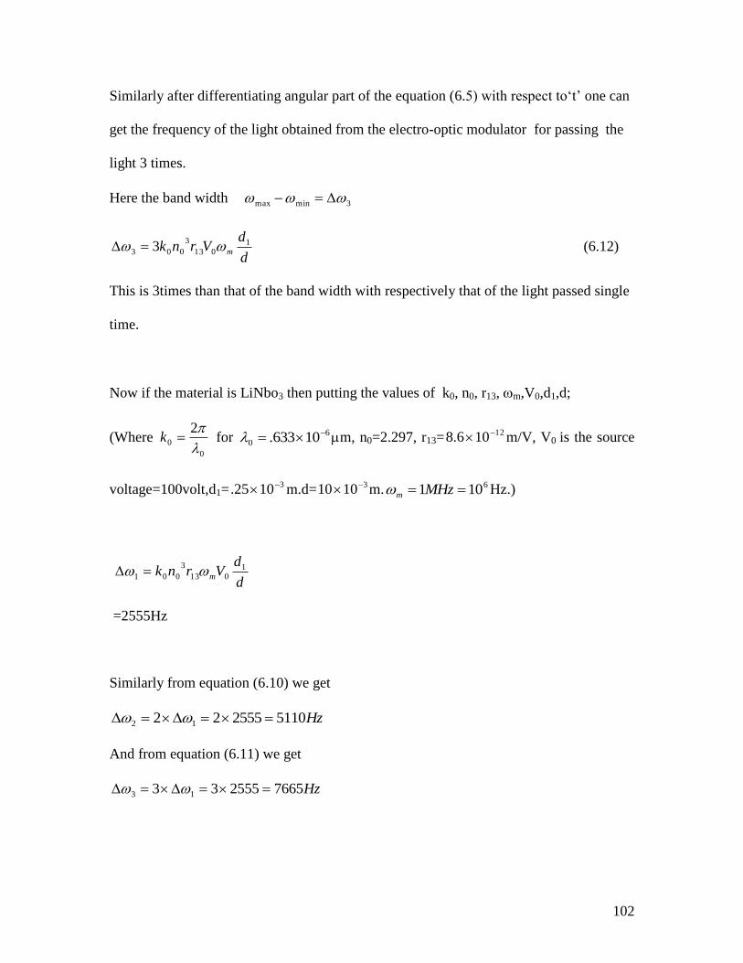
102
Similarly after differentiating angular part of the equation (6.5) with respect to‘t’ one can
get the frequency of the light obtained from the electro-optic modulator for passing the
light 3 times.
Here the band width 3minmax
d
dVrnk m
1013
3
003 3 (6.12)
This is 3times than that of the band width with respectively that of the light passed single
time.
Now if the material is LiNbo3 then putting the values of k0, n0, r13, m,V0,d1,d;
(Where 0
0
2
k for 6
0 10633. m, n0=2.297, r13=12106.8 m/V, V0 is the source
voltage=100volt,d1=31025. m.d= 31010 m. 6101 MHzm Hz.)
d
dVrnk m
1013
3
001
=2555Hz
Similarly from equation (6.10) we get
Hz5110255522 12
And from equation (6.11) we get
Hz7665255533 13
103
After 3times rotation it is seen that the band width is till far lower than 1MHz.Now
rotating the single multiple time the band width may be increased to 1MHz not increasing
V0,d1,d etc.
6.5 Conclusion:
It is concluded that the bandwidth of a signal passing through the electro-optic modulator
increases for multi passing of the beam through the modulator. For n time passing of the
beam the bandwidth increases also n times. The phenomenon is the very much helpful for
analog optical communication, which requires high band width and also in frequency
conversion.

104
References
6.1) L.Wooten, K.M.Kissa, A.YiYan, E.J.Murphy, D.A.Lafaw, P.F.Hallenmeir,
D.Maack, D.V.Attanasio, D.J.Fritz, G.J.McBri and D.E.Bossi, “A review of
lithium niobate modulators for fiber-optic communicatins systems.”IEEE
J.Sel.Top.Quantum Electron.6,69-82(2000).
6.2) L.E.Myers,R.C.Eckardt,M.M.Fejer,R.L.Byer,W.R.Bosenberg and J.W.Pierce,
“Quasi-phase-matched opticalparametric oscillators in bulk periodically poled
LiNbO3,”J.Opt.Soc.Am.B12,2102-2116(1995).
6.3) Yi Liao,Huijuan Zhou and Zhou Meng, “Modulation efficiency of aLiNbO3
waveguide eletro-optic intensity modulator operating at high microwave
frequency”,Optics Letters Vol.34,No.12,June 15,2009.
6.4) Benedict.J.Cuasack, Benjamin.S.Sheard, Daniel.A.Shaddock, Malcolm.B.Grray,
Ping Koy Lam, AND Stan E.Whitcomb, “Electro-optic modulator capable of
generating simultaneous amplitude and phase modulations”,Applied optics
Vol.43,No.26(2004).
6.5) D.Janner,D.Tulli,M.Belmonte and V.Purneri “Wave guide electr-optic in micro-
engineered LiNbO3.”Pure and applied optics,Vol10,No-10.(2008).
6.6) Abhijit Sinha, Harihar Bhowmik, Puspendu Kuila, S. Mukhopadhyay, “New
method of controlling the power of a Gaussian optical pulse through an electro-
optic modulator and a nonlinear wave guide for generation of solitons”, Optical
Engineering, 44(6), 065003(1 June, 2005).

105
6.7) Puspendu Kuila, Abhijit Sinha, Harihar bhowmik, S. Mukhopadhyay,
“Theoretical study of using an amplitude modulation scheme with an electro-optic
modulator for generation of the proper power shape function of an optical soliton
pulse in a nonlinear waveguide”, Optical Engineering, 45(4), 045002(2006).
6.8) Takanori Shimizu,Masafumi Nakada,Hiroki Tsuda,Hiroshi Miyazaki,Jun Akedo
and Keishi Ohashi “Gigahertz-rate optical modulation on Mach-Zehnder Plzt
electro-optic modulators formed on silicon substrates by aerosol deposition”
IEICE electronics express Vol 6(2009).No.23 PP 1669-1675.
6.9) Mao-Sheng Huanga and Mao-Hong Lu “High sensitivity bulk electro-optic
modulator field sensor for high voltage environments” Review of scientific
instruments Vol.75.n0.12(2004).
6.10) Liao,Yi.Zhou,Huijuan and Meng.Zhou “Modulation efficiency of a LiNbO3 wave
guide electro-optic intensity modulator operating at high microwave
frequency.”Optics Letters 2009-06-15.
6.11) Zaldzvar-Huerta, and J.Roderzguez-Asomoza “Electro-optic E-field using an
optical modulator”, doi: iceee computers society org/ 10.1109/ ICECC. 2004.
1269576.
6.12) Ross T.Sehemer,Frank Bucholtz,Carl A.Virruel,Jesus Gil Gil,Tim D.Andreadis
and Keith J.Willams “Investigation of electro-optic modulator disruption by
microwave induced transients”Optics Express Vol.17,Issue 25.PP.22586-
22602(2009).

106
6.13) S.Haxha,B.M.A.Rahman and R.J.Langley “Broadband and low driving power
LiNbO3 Electro-opticmodulators”Optical and Quantum electronics
Vol.36.No.14(2004).
6.14) Liao Y,Zhou H.Meng .Z, “Modulation efffiency of a LiNbO3 wave guide electro-
optic intensity modulator oprating at high microwave frequency.”Optics Letters
2009.34(12):1822-4.
6.15) G.L, Li, P.K.L and Yu “Optical intensity modulators for digital and analog
applications”Journal of light waves Technology,Vol.21, Issue 9, PP2010(2003).
6.16) D.Janner ,D.Tulli and M.Belmonte ,V.Pruneri “Micro-engineered integrated
electro-optic modulators in LiNbO3 Lasers and Applications,Vol.992
PP.254259(2009).

107
CHAPTERVII
Some Analytical Study on Optical Velocity Modulation
by Electro-Optic Modulator
Abstract:
Electro-optic materials have the well known applications in several modulations of
optical waves. Intensity modulation, phase modulation etc. are the types of modulations
which can be conducted easily by electro-optic modulators, which use the Pockels effect
in such modulations. The conventional electro-optic materials like KDP, LiNbO3 etc. are
very much popular devices for optical modulations. Here in this chapter I show some
interesting characters of Electro-Optic materials in the case of Optical Velocity
Modulation.
Papers associated with this chapter
1) R.Maji and S.Mukhopadhyay “Some analytical investigation on propagations of
radiation in elecro-optic modulator in connecion tooptical velocity modulation” ,IUP
journal of Physics,Vol- iv No-4 pp-25 29 (Oct2011).

108
7.1 Introduction:
When a beam passes through an electro-optic modulator biased by an electric field then
the velocity of the beam is modulated. When a beam of plane wave front passes through
a linear optical medium the phase velocity for all the rays in the beam remains same, if
the medium is non-guiding in nature. If the medium is not a linear one, ie its refractive
indices offered to the rays are different for different wave length than the question of
group velocity will necessarily come. Electro-optic material is an example of one such
material [7.1, 7.2, and 7.3]. Here the refractive index offered to the rays is dependent on
the applied field on it and also on the wave length .So when a plane wave travels through
such a medium, the beam faces a time changing refractive index if an alternating electric
field is applied to the material. The major practical use of an electro-optic material lies in
modulation of the beam passing through it [7.4, 7.5, and 7.6]. Therefore in the area of
communication and data processing such materials can show a strong role. In the above
use of beam modulation generally the time varying electric field is applied as a message
signal. To achieve an electro-optic Q-switching electro-optic materials are also strongly
used [7.9, 7.10, and 7.11].
Here in this chapter I am interested to show that when a beam of plane wave front
travels through an electro-optic pockel’s material like KDP(Potassium dihydrogen
Phosphate),LiNbo3(Lithium Niobate) etc. supported by some externally biased
alternating electric field, it faces a time varying refractive index in the medium, and there
by a time varying group velocity will be obtained which is extremely useful when such
plane waves are used as optical pulses in digital communication through optical fiber and

109
also in other applications. In the following treatment an expression relating the variation
of group velocity with the specific electric field applied to an electro-optic modulator is
established.
7.2 Properties of Potassium Dihydrogen Phosphate
and Potassium Dideuterium Phosphate (KDP and
KD*P crystals):
Potassium Dihydrogen Phosphate (KDP) and Potassium Dideuterium Phosphate (KD*P )
are among the most widely-used commercial NLO materials. They are commonly used
for doubling, tripling and quadrupling of the frequency from Nd:YAG laser at the room
temperature. In addition, they are also excellent and useful electro-optic crystals with
strong electro-optic coefficients, widely applied as electro-optical modulators, Q-
switches, and Pockels Cells, etc [7.7, 7.8].
Fig-7.1 Kdp Crystal

110
7.3 KDP as electro-optic modulator:
Normally in absence of externally applied field KDP crystal shows its uniaxial character .
The crystal generally accommodates a four fold axis of symmetry, for which a rotation of
the crystal structure against the axis by an angle 2π/4 keeps the crystal geometrically
invariant and these axis is referred as the Z-axis or the optic axis of the crystal. Also they
occupy the two more orthogonal axes of symmetry designated as X and Y axes about
which the crystal structure support an invariance after a rotation of π .These are referred
as two fold symmetry. Actually one can exploit electro-optic effect in KDP crystal both
in the longitudinal mode as well as in transverse mode [7.1, 7.2, and 7.3].
First a linearly polarized plane wave (polarized along X direction) is considered which
is propagated along the Z-direction in a KDP crystal of length .Now an external electric
field is applied along the same Z-direction and therefore the refractive index of the light
will change accordingly (fig.7.1). The resulting output beam therefore becomes a phase
modulated beam due to Pockel effect of the KDP crystal.
Fig-7.1 The phase modulation with KDP crystal.
X
Y
z
KDP crystal
VZ Pass
axis X
polarizer
Modu
lated
out
put
beam
Z
x
Y

111
7.4 Field modulated refractive index in electro-optic
modulator:
The refractive index )( xn for wave polarized along X -direction of a KDP crystal for
the rays passing through the Z axis is[7.1,7.2] given by
Zx REnnn )(2
1 3
00 (7.1)
Where n0 is a constant refractive index term of KDP, R is a material constant of KDP and
EZ is the externally applied electric field in the KDP along Z direction.
Similarly if the beam polarized along Y direction is sent along the Z direction then the
refractive index is given by
Zy REnnn )(2
1 3
00 (7.2)
Now for alternating nature of the external field,
tEE mZ sin0 (7.3)
Where xn , yn are expressed respectively by putting the value of eqn (7.3) in eqn (7.1)
we get,
)sin(2
10
3
00 tREnnn mx (7.4)
And putting the value of eqn (7.3) in eqn (7.2)
We get,
)sin(2
10
3
00 tREnnn my (7.5)

112
Here E0 and m are the amplitude and frequency of the externally applied electric signal
to the modulator.
Thus if a light polarized along 450 to both X and Y axes passes through the elecrto-
optic modulator along the Z axis, the X component of the light will go with the
velocity xX nCV / (7.6)
and light polarized along Y direction will pass with the velocity
yY nCV / (7.7)
Here C is the free space velocity of light.
7.5 Different velocities achieved by the components of
the waves:
The expression of the minimum velocity of the X component wave is
(7.8)
The expression of the maximum velocity of the X component wave is,
))(2
1/( 0
3
00max, REnnCVX (7.9)
Similarly, the minimum velocity of the Y component wave is,
(7.10)
Similarly, the maximum velocity of the Y component wave is,
(7.11)
From the treatment it is seen that when the X component wave travels with maximum
velocity, the Y component wave travels with the minimum, and when the X
))(2
1/( 0
3
00min, REnnCVX
))(2
1/( 0
3
00min, REnnCVY
))(2
1/( 0
3
00max, REnnCVY

113
component wave travels with the minimum velocity, Y component wave travels with the
maximum velocity through the electro-optic modulator. The difference between the
maximum velocity and minimum velocity for both waves are same.
SO,
min,max,min,, XXYmzxY VVVV (7.12)
Again, as the value of R is very small for KDP crystal the expression of the velocity of
the X component wave can be written as
)]sin(2
11[/ 0
2
00 tEnnCV mX (7.13).
Similarly, the velocity of Y component wave can be written as,
)]sin(2/11[/ 0
2
00 tEnnCV mY (7.14)
The acceleration of the wave can be calculated from the earlier equations .If AX and AY
are the accelerations of the X component wave and Y component wave respectively
then differentiating eqn (7.13) and eqn (7.14) with respect to time ‘t’ we get
mmOX
X tRCEndt
dVA )].(cos[
2
10 (7.15)
And
mmY
Y tRCEndt
dVA )].(cos[
2
100 (7.16)
mmX tRCEnA )].(cos[2
100 (..7.17)
And
mmY tRCEnA )].(cos[2
100 (7.18)

114
7.6 Conclusion:
In this chapter it is discussed, how the velocity of light beam is modulated by change of
refractive index of the used non linear material by the application of an external electric
field. From the above treatment it is seen that the velocities of the X component wave
and Y component wave through the modulator are modulated linearly with the applied
sinusoidal electrical signal EZ. In the same way, accelerations are also linearly modulated
by the applied electrical signal along the Z axis. It is also concluded that when there is
acceleration in the X component of the signal, deceleration is found in the Y
component of the signal. However the modulation indices of the velocity modulation are
same for both the components of light. In case of velocity modulation the dc bias value is
(C/n0), Finally it can be concluded that as the velocity modulation offers a faithful
modulation, so a here a distortion less optical communication may be achieved as an
alternative of other modulation. This velocity modulation may be a very useful technique
in modern day’s high speed communication system.

115
References
7.1) Ajoy Ghatak and K.Thyagarajan “Optical Electrnics”, (Cambridge university
press 2002).
7.2) A., Yariv , Wiley, “Optical Electronics”,(1989) New York.
7.3) A.Yariv.and P.Yeh, John Wiley and Sons,, “Optical waves in crystals
Propagation and control of laser radiation” (2003), New York.
7.4) Abhijit Sinha, Hariar Bhowmik, Puspendu Kulia and Sourangshu Mukopadhyay;
“New method of controlling the power of a Gaussian optical pulse through an
electro-optic modulator and a non-linear wave guide for generation of solitons”
,Optical Engineering June 2005/vol.44(6).
7.5) Puspendu Kuila , Abhijit Sinha , Harihar Bhowmik and Sourangshu
Mukhopadhyay “A Theoretical Study of using amplitude modulation Scheme of
an eletro-optic modulator for generation of proper power shape function of an
optical soliton in a non linear wave guide”, Optical Engineering,Vol 45 , U.S.A
2006.
7.6) Abhijit Sinha and Sourangshu Mukhopadhyay- “Effect of higher order non-
linearity in frequency variation of self-phase modulation in optical fiber
communication,Chinese optics letters.Vol.2,No.9/September 10,2004.
7.7) L.R.Dalton “Rational Design of organic Electro-optic materials,”
J.Phys.Condens.matter,15, R897-934,(2003).

116
7.8) C.Thang, L.R.Dalton, M.C.ah,H.Thang, and W.H.Steier “Low V? Electro-optic
Modulators from CLD-1:Chromoophore Design andsynthesis, Materials
Processing, and characterization,” Chem.Mater,13,3043-50,(2001).
7.9) L.Duvillaret, S.Rialland, J.Louis Coutaz “Electro-optic sensors for electric field
measurements.1.Theoritical comparison among different modulation techniques”
JOSAB, vol 19,issue 11,PP2692-2703,doi:10.1364/JOSAB.19.002692.(2002).
7.10) Zhang, X.C “Free space electro optic sampling of terahertz beams” Applied
Physics Letters, vol.67, issue.24 PP3523-3525, doi:10.1063/1.114909(1995).
7.11) M.Delgado. Pinar, D.Zalvidea, A.Diez, P.Perez-Millan and M.Andres “Q-
switching of an all-fiber laser by acousto-optic modulation of a fiber Bragg
grating” Optics Express,vol.14, issue 3,PP1106-
1112,doi:10.1364/OE.14.001106.(2006).

117
CHAPTER VIII
An Alternative Optical Method of Determining the
unknown Microwave Frequency by the use of Electro-
Optic Materials and Semiconductor Optical Amplifier.
Abstract:
There are found different established methods for measuring the frequency of an
unknown microwave signal [8.1]. Here in this chapter I propose a new concept of
measuring unknown microwave signal with the joint uses of reflecting semiconductor
optical amplifier (RSOA) and electro-optical Pockel material. To measure the frequency
a variable known and calibrated microwave frequency is required. Then with the help of
a RSOA and electro-optic material one can find a unknown microwave frequency more
accurately than that of the frequency measured by conventional mechanism. This method
can give the high degree of accuracy of the measurement of the applied frequency as
optics is used to measure a unknown microwave frequency. Here the electro-optic
material takes the role of phase modulation.
Papers associated with this chapter
1) R.Maji,S.Mukhopadhyay“An alternative optical method of determining the unknown
microwave frequency by the use of electro-optic materials and semiconductor optical
amplifier” , Optik international journal for Light Electron optics vol-122,issue 18 pp
1622-1624 (2011) doi:10.1016/ijleo.2010.10.013.
2) R.Maji,S.Mukhopadhyay “An alternative optical method of determining the unknown
microwave frequency by the use of electro-optic materials and semiconductor optical
amplifier”, Int conference on radiation Physics and its application organized by The Univ
of Burdwan Department of PhysicsNat 17 th jan ( ICRPA2010).

118
8.1 Introduction:
Microwaves are electro-magnetic waves with wavelengths ranging from one meter to as
short as one millimeter, with frequencies between 300 MHz to 300 GHz. This broad
range includes both UHF and EHF. In all cases, microwave includes also the entire SHF
band (3 to 30 GHz, or 10 to 1 cm) with RF engineering for lower boundary at 1 GHz
(30 cm), and the upper around 100 GHz (3 mm).Microwave frequency measurement
based on photonic techniques has attracted significant interest recently. The primary
advantages of microwave frequency measurement in the optical domain are the real time
and high accuracy which may not be achievable using conventional electronic
techniques.Microwave is a well electromagnetic established carrier for the transportation
over a long distance. In high speed communication there is seen a tremendous need for
measuring the frequencies of both modulated as well as the unmodulated signal in the
microwave range. Several resonating and electronic methods are found for measuring the
frequency of an unknown wave [8.2, 8.3, and 8.4]. Each method has its own advantage.
Here in this chapter I propose a new concept of measuring unknown microwave signal
with the use of electro-optic material and semiconductor optical amplifier jointly. One
known microwave frequency is also used to measure the unknown microwave frequency.
This process ensures the highest degree of accuracy.
Electro-optic material and a special type of semiconductor optical amplifier, known as
reflecting semiconductor amplifier, are used to find the correct frequency of an unknown
microwave signal.

119
8.2 Electro-optic materials (EOM):
The simplest kind of EOM (electro-optic material) consists of a crystal, such as Lithium
Niobate, whose refractive index is a function of the strength of the applied electric field.
That means if Lithium Niobate is exposed to an external electric field, light can travel
more slowly through it under some special condition. But the change of phase of the light
leaving the crystal is directly proportional to the length of the crystal and the applied
field. Therefore, the phase of a laser light exiting an EOM can be controlled by changing
the electric field in the crystal [8.5, 8.6, 8.7, and 8.8].
A very common application of EOMs is for creating sidebands in a monochromatic laser
beam.
8.3 Application of Semiconductor optical amplifier
(SOA):
There are several applications of SOA, some of the applications of SOA are listed as
follows.
a) In all optical signal processing like all-optical switching and wavelength
conversion.
b) In clock recovery.
c) In signal demultiplexing.
d) In pattern recognition.
e) Four wave mixing.
f) Cross gain modulation.
g) Cross phase modulation.

120
8. 4 Semiconductor optical amplifier (SOA) and
Reflecting semiconductor amplifier (RSOA) used
as add/drop multiplexer.
Semiconductor optical amplifiers are the optical amplifiers which use a proper
semiconductor to provide a gain medium. These amplifiers have a similar structure to that
of Fabry-Perot laser diodes generally with a anti-reflection coatings at the end faces. A
recent design of SOA accommodates an anti-reflection coating, which can reduces the
end face reflection to less than 0.001%. As it creates a power loss from the resonators
cavity greater than the gain of the cavity so these amplifier can not act as a laser [8.9].
Semiconductor optical amplifiers(SOAs) are generally made from group III-V compound
semiconductors like GaAs or AlGaAs, InP or InGaAs, InP or InGaAsP and InP or
InAlGaAs. These types of amplifiers are very often used in fiber optic communication
systems, etc, at the operating the wavelengths between 0.85 µm and 1.6 µm and it can
provide a gain of up to 30 dB.
In an SOA carrier electrons are injected from an external biasing current source into its
active region. These energized carriers are then distributed in the energy states of its
conduction band (CB) region, leaving holes in the valence band (VB). Generally four all-
optical nonlinear processes are found in semiconductor optical amplifier. They are , (i)
Cross gain modulation (ii) Cross phase modulation (iii) Optical wavelength conversion
(iv) Self phase modulation. Several all optical switching devices, logic families, optical
processors can be developed using one or more than one switching mechanisms of SOA
[8.10, 8.11, 8.12, 8.13, 8.14, 8.15].

121
On the other hand a Reflective Semiconductor Optical Amplifier (RSOA) can
compensate the light loss in an optical system. The polarization dependency in RSOA is
also improved.
8.5 Optical Method for Determination of Unknown
Microwave Frequency:
A laser light of frequency1 is taken. This wave is passed through the electro-optic
modulator.
Fig-8 A Scheme of finding out the unknown microwave frequency using electro
optic modulator and reflecting semiconductor amplifier.(F1 and F2 optical filters,
EOM is electro-optic modulator, RSOA is Reflecting semiconductor optical
amplifier, Ii s ammeter).
1ST
EOM
2ND
EOM
c RSOA
OA
1
I
Unknown Known
1
m c
F1 F2

122
The field of the laser beam is expressed as then E1, Where
)( 11011 tCosEE ( 8. 1 )
The external electric field applied on the electro-optic modulator is EM, where
)cos(0 tEE mMM ( 8. 2 )
Here 1, are the phases of these two signals.
The non-linear refractive index n of the electro-optic material (i.e LiNbO3) is
Mee Ernnn 033
3
2
1 (8.3)
Where ne is refractive index of the LiNbO 3 crystal when the external field is not applied
and 33r is its electro-optic material co-efficient.
After passing through the electro-optic modulator E1 becomes
]cos[011 kntEE (8.4)
Now putting the values of eqn (8.2) and eqn (8.3) in eqn (8.4)
We get,

123
)]cos(2
1)cos[( 033
3
1011 tkErnkntEE mMee (8.5 )
Where the width of the electro-optic material and k is is the free space wave number of
the laser radiation.
Now, from equation (8.5) one can
g ])2()2(2
2cos{()(
})()(2
cos{)()cos()([
1112
11111110011
knttJ
knttJkntJEE
em
eme
(8.6)
Where kErn Me 033
3
12
1
(8.7)
The output of the modulator is then passed through an optical filter F1 which passes all
the frequencies below1 .
The emitted light from the optical filter passes through 2nd
electro-optic modulator .The
expression of the external electric field applied on the electro-optic modulator is
)cos( 2 tEE cocc (8.8)
After passing through the 2nd electro-optic modulator the electric field of the light
E1becomes
1E which is

124
(8.9)
The modulated output of the 2nd
electro-optic modulator is passed through reflecting
semiconductor optical amplifier. Now when c (the taken microwave frequency) matches
with m (the unknown microwave frequency) the output of the 2nd
electro-optic
modulator gives a signal of frequency of 1 including many other frequencies like
mm 4,2 11 ……. .Now a second optical filter (F2) is put after the 2nd
electro-
optic modulator. This filter only passes the 1 frequency.
The unknown microwave is applied at the 1st electro-optic modulator. The output of the
modulator is passed through the 1st optical filter which passes all the frequencies below
1 .Now the modulated output from the 1st electro-optic modulator is passed through the
2nd
electro-optic modulator which is triggered by an electro-optic signal of known
frequency c , which can be varied linearly. The modulated output of the beam coming
for the 2nd
electro-optic modulator is passed through reflecting semiconductor optical
amplifier (RSOA). Now as and when c matches with m the output of the 2nd
electro-
optic modulator gives a frequency of 1 .Therefore The RSOA reflects it as output, as it
is already biased electrically to reflect 1 .
]})22(2
2cos{)(
})()(2
cos{)(
)cos()([
21112
21111
11100011
kntttJ
kntttJ
kntJEEE
ecm
ecm
ec

125
So if one obtains 1 at the output, it can be concluded that c (known) is the proper
frequency of the unknown microwave signal applied to the EOM.
8.6 Conclusion:
In this chapter I proposed a novel concept for unknown microwave frequency
measurement with the help of known microwave frequency. The method described above
gives an optical approach to find out an unknown microwave frequency. As an optical
frequency (4 1510 Hz to 8 1510 Hz) is very much higher than that of a microwave
(300MHz to 300GHz) one so the measured frequency produces a high degree of
accuracy. The highest value of microwave frequency depends on the response of the
electro-optic modulator used. So a better electro-optic modulator will serve a better
response for the measurement of unknown microwave signal.

126
References
8.1) J.Zhou,S.Fu,Shum and P.P,Chinlon Lin “Instantaneous microwave frequency
measurement using photonic technique”Photonics Technology Letters,IEEE
vol.21,issue 15,PP 1069-1071,doi:10.1109/LPT.2009.2022637(2009).
8.2) Hao Chi,Xihua Zou and Jianping Yao, “An approach to the measurement of
Microwave frequency based on optical power monitoring”, IEEP Photonics
technology letters,vol.20,No.14,July 15,2008.
8.3) L.V.T Nguyen and D.B.Hunter “A photonic technique for microwave frequency
measurement”,IEEE.Photon.Technol.Lett,vol.18,10,pp.1188-1190,May 15,2006.
8.4) Ghislaine Maury,Attila Hilt,Tibar Berceli and Beatrice Cabon, “Microwave
Frequency conversion methods by optical interferometer and photodiode”,IEEE
TRANSACTIONS on Microwave theory and techniques,vol.45,No.8,August
1997.
8.5) A.Sinha,H.Bhoumik,P.Kuila and S.Mukhopadhyay, “New method of controlling
the power of a Gaussian optical pulse through an electro-optic modulator and a
non-linear wave guide for generation of solitons”, opt.
Eng,44(6)(065003)June(2005).
8.6) A.Ghatak and K.Thayagarajan Optical electronics (Cambridge university press
2002).

127
8.7) Prasanta Mondal and S.Mukhopadhyay, “Method of conducting an ll-optical
NAND logic operation controlled from a long distance”, optical
Engineering(USA),46(3),035009(2007).
8.8) P.Mondal, H.Bhowmik and S.Mukhopadhyay,” All-optical method of conducting
long distance switching by proper use of an electro-optic Pockels material and a
non-linear optical wave guide”, optical Engineering(USA),45(7),075002(2006).
8.9) Semiconductor optical amplifier by Michel .J. Connelly (Kluwer Academic
publishers, U.S.A (2002).
8.10) S.K.Garai and S.Mukhopadhyay, “A method of optical implementation of
frequency encoded different logic operations using second harmonic and
difference frequency generation techniques in non-linear material”, optic-
International journal for light and electron optics, published on line on 21st
May,(2009).
8.11) Z.Li and G.Li, “Ultrahigh speed reconfigurable logic gates based on four-wave
mixing in a semiconductor optical amplifier,” IEEE Photonics technology letters,
vol.18.No.12,June 15,2006.
8.12) S.K.Garai, and S.Mukhopadhyay, “Method of implementating frequency encoded
multiplexer and demultiplexer systems using nonlinear semiconductor optical
amplifier”,optics and laser technology,41(8),972-976(2009).

128
8.13) S.K.Garai and S.Mukhopadhyay , “Method of implementation of all-optical
frequency encoded logic operations exploiting the propagation characters of light
through semiconductor optical amplifiers, “Journal of optics, 38(2),88-102(2009).
8.14) Jae-Hunkim,Young Tae Byun,Young Minjhon ,Seok Lee,Deok Ha Woo and Sun
Hokim, “All-optical half adder using semiconductor optical amplifier based
devices”,optics communications vol.218,issues4-6,27 february
2003.doi:10.1016/50030-4018(03)01203-3.
8.15) K.LHall and K.A.Rauchenbach, “100-Gbit/s bitwise logic”, optics letters,vol.23,
issue 16,pp.1271-1273 doi:10.1364/OL.23.001271.

129
CHAPTER IX
Conclusion and future scope of study:
Abstract:
In this chapter a general conclusion of the whole thesis is included. At the same time the
possible future scope of work related to my present contributed works described in the
thesis are also given in this chapter.

130
9.1 Introduction:
Till now Several works have been done by several scientists on the area of application of
Electro-optic material, which are useful for optical communication, data processing, all
optical system, optical computing etc. As there are some limitations in electronic high
speed passing to remove this limitations in present day much of our used electronics
could soon be replaced by photonics because of photonic chips would carry more data,
use less power and work smoothly with fiber optic communication systems.
There are some limitations and difficulties to implement Electro-optic modulator based
communication systems with full satisfaction. These difficulties arise mainly from proper
availabilities of Electro-optic modulator, low power lasers, and development of proper
analytical methods for organizing the experiment.
9.2 Proper availability of Electro-optic modulators:
In many cases the success of optical communication very much depends on proper
availability of Electro-optic modulators. Constant Electro-optic modulators are large in
shape and are applied in high voltages (in KV order).Therefore they consume high
power, which is normally expensive for communication system. Therefore it is essential
to develop small size (sub micron level), low power consuming Electro-optic modulator,
which will be suitable for integrated photonic circuits. There are found several proposals
on some useful practical electro-optic modulators in the literature, but the applications of
this type of low powered, small dimension electro-optic (Pockel’s type) modulators are
still in now primary stage recently.
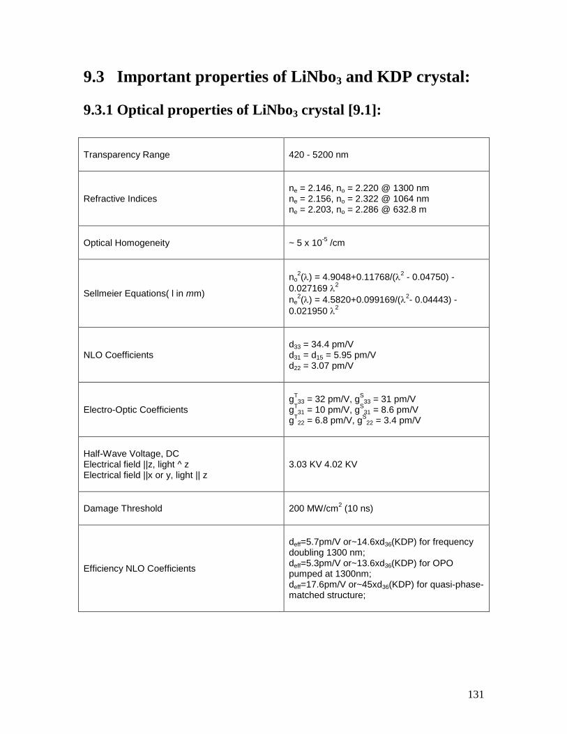
131
9.3 Important properties of LiNbo3 and KDP crystal:
9.3.1 Optical properties of LiNbo3 crystal [9.1]:
Transparency Range 420 - 5200 nm
Refractive Indices ne = 2.146, no = 2.220 @ 1300 nm ne = 2.156, no = 2.322 @ 1064 nm ne = 2.203, no = 2.286 @ 632.8 m
Optical Homogeneity ~ 5 x 10⁻⁵
/cm
Sellmeier Equations( l in mm)
no2() = 4.9048+0.11768/(
2 - 0.04750) -
0.027169 2
ne2() = 4.5820+0.099169/(
2- 0.04443) -
0.021950 2
NLO Coefficients d33 = 34.4 pm/V d31 = d15 = 5.95 pm/V d22 = 3.07 pm/V
Electro-Optic Coefficients g
T33 = 32 pm/V, g
S33 = 31 pm/V
gT
31 = 10 pm/V, gS
31 = 8.6 pm/V g
T22 = 6.8 pm/V, g
S22 = 3.4 pm/V
Half-Wave Voltage, DC Electrical field ||z, light ^ z Electrical field ||x or y, light || z
3.03 KV 4.02 KV
Damage Threshold 200 MW/cm2 (10 ns)
Efficiency NLO Coefficients
deff=5.7pm/V or~14.6xd36(KDP) for frequency doubling 1300 nm; deff=5.3pm/V or~13.6xd36(KDP) for OPO pumped at 1300nm; deff=17.6pm/V or~45xd36(KDP) for quasi-phase-matched structure;
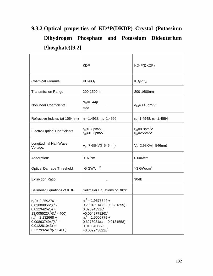
132
9.3.2 Optical properties of KD*P(DKDP) Crystal (Potassium
Dihydrogen Phosphate and Potassium Dideuterium
Phosphate)[9.2]
KDP KD*P(DKDP)
Chemical Formula KH2PO4 KD2PO4
Transmission Range 200-1500nm 200-1600nm
Nonlinear Coefficients d36=0.44p
m/V d36=0.40pm/V
Refractive Indcies (at 1064nm) no=1.4938, ne=1.4599 no=1.4948, ne=1.4554
Electro-Optical Coefficients r41=8.8pm/V r63=10.3pm/V
r41=8.8pm/V r63=25pm/V
Longitudinal Half-Wave Voltage:
Vp=7.65KV(l=546nm) Vp=2.98KV(l=546nm)
Absorption: 0.07/cm 0.006/cm
Optical Damage Threshold: >5 GW/cm2 >3 GW/cm
2
Extinction Ratio: 30dB
Sellmeier Equations of KDP: Sellmeier Equations of DK*P
no2 = 2.259276 +
0.01008956/(2 -
0.012942625) +
13.0055222/(
2 - 400)
ne2 = 2.132668 +
0.008637494/(2 -
0.012281043) +
3.22799242/(
2 - 400)
no2 = 1.9575544 +
0.2901391/(2 - 0.0281399) -
0.028243912
+0.0049778264
ne2 = 1.5005779 +
0.6276034/(2 - 0.0131558) -
0.010540632
+0.0022438214

133
9.4 Final conclusion and proposed future study:
In my Ph.D work I have shown some new methods of using electro-optic materials and
non-linear materials for getting better implicational advantages for the purpose of
optical modulation.
In my first work I have shown that if an electro-optic Pockel cell is used before a Kerr-
cell, which extends the self-focusing, then one can easily control the focal length of the
self-focusing system and the defocusing length can also be controlled by the same
mechanism by applying the desired amount of voltage at the electro-optic material. The
whole scheme may extend a tremendous application in optical communication through
optical fiber. In my second Work I have shown the nature of variation of intensity /power
of the harmonic signals obtained at the output of the electro-optic modulator, which
depends on the number of passing of radiation through the modulator. The propose
scheme will be beneficial for increasing the harmonic power of the radiation passing
through the electro-optic modulator by multi-passing mechanism. Generally the power of
the central frequency is wastage at the time of phase/frequency modulation, where the
powers of the harmonics are important for practical application. In the present scenario
the harmonic power increases making the power of central frequency decreased. In my
next work I have shown that by using multi passing technique through electro-optic
modulator it can be possible to reduce the half-wave voltage of the crystal. The V for
KDP is very high in comparison to LiNbO3.This V can be reduced as far as practicable
by the adoption of the above method. After reduction of V a signal of small amplitude
can be modulated with the electro-optic modulator .Thus this method can extend a wide

134
application and advantage for optical guided wave communication. This work may give
some concrete advantages in connection to the electrical power requirement for all optical
modulation. In my next work I explained that the bandwidth of the electro-optic
modulator increases for multi passing of a beam through the modulator. The phenomenon
is the very helpful for analog optical communication, which requires high band width.
After that I have explained, how the velocity of light beam is modulated due to change of
refractive index of the used non linear material by the application of an external electric
field. In case of velocity modulation the dc value is (C/n0), finally it can be concluded
that as the velocity modulation offers a linear modulation so a non linear distortion less
optical communication may be preferred as an alternative of other modulation. This
velocity modulation is very useful in modern communication system. In my next work I
have shown a novel concept for unknown microwave frequency measurement with the
help of known microwave frequency. The method described above gives an all optical
approach to find out an unknown microwave frequency. As an optical frequency is very
much higher than that of a microwave one so the measured frequency gives a high degree
of accuracy. This work has already been cited by some other authors in reputed journals
[9.3, 9.4, and 9.5]. These finding here are not obtained by other researcher earlier.
9.5 Future scope of work:
In future I will try to verify the above results experimentally. I will also propose some all
optical methods of incrementing binary, trinary logic based switches with electro-optic
materials and non-linear materials. In future I will give also an effect to use the
conventional electro-optic modulators in high speed optical switched based circuits.

135
9.6 Conclusion:
This chapter includes the overall conclusion of the whole thesis. Along with it the future
scope of work in connected to the present work is also described .I believe the readers of
the thesis will get some interest while going through the thesis.

136
References
9.1) www.redoptronics.com/linbo3 –crystal .html.
9.2) www.redoptronics.com/KDP-crystal.html.
9.3) Y. Gu; J. Hu; S. Li; X. Han; M.Wang; P. Wu and M.Zhao “Novel photonic
broadband microwave frequency measurement based on intensity-modulated link
with output microwave interference detection”, Optical Engineering 51(1),
019001, DOI: 10.1117/1.OE.51.1.019001(2012).
9.4) S. Hu X. Han ; P. Wu ; Y. Gu ; and M. Zhao “A photonic technique for
microwave frequency measurement employing tunable dispersive medium “,
Microwave Photonics, 2011 International Topical Meeting on & Microwave
Photonics Conference, 2011 Asia-Pacific, MWP/APMP”IEEE,165-168,DOI:
10.1109/MWP.2011.6088695.
9.5) Shu Hu ; Xiuyou Han ; Pengsheng Wu ; Yiying Gu ; Jingjing Hu and Mingshan
Zhao “Optical approach for measuring unknown microwave frequency with
improved sensitivity” Optical engineering, Vol 52,issue
2,doi:101117/1.OE.52.2.025002(2013).