Embed Size (px)
Citation preview

10.1098/rsta.2003.1344
Surface plasmon polaritons inmetal stripes and wires
By J. R. Krenn1
and J.-C. Weeber2
1Institute for Experimental Physics and Erwin Schrodinger Institute forNanoscale Research, Karl–Franzens University Graz, 8010 Graz,
Austria ([email protected])2Laboratoire de Physique de l’Universite de Bourgogne,
Optique Submicronique, BP 47870,21078 Dijon, France
Published online 12 February 2004
Surface plasmon polaritons (SPPs) are collective electron oscillations coupled to alight field which are propagating along the interface of a metal and a dielectric.As a surface wave, SPP modes feature properties essentially different from light-field modes in all dielectric structures. These properties could allow the realizationof novel photonic devices that overcome certain limitations of conventional devices.Specifically, the realization of two-dimensional optics and light-field transport in sub-wavelength SPP waveguides seems feasible. In this review we discuss recent exper-imental advances regarding SPP waveguides, i.e. laterally confined metal thin filmsthat guide SPPs. Electron-beam lithography is applied to tailor these films withwidths ranging from a few micrometres (stripes) to nanoscopic values (wires). Weinvestigate SPP properties such as propagation length, mode field profile and reflec-tion or scattering at interfaces. Various techniques for SPP excitation and detectionare discussed.
Keywords: surface plasmon polaritons; metal waveguides; nano-optics;scanning near-field microscopy
1. Introduction
The continuous miniaturization of existing electronic devices is expected to meetfundamental limitations in the near future. For example, the metallic interconnectsused to link individual electronic elements within data-processing units as well asinterfacing these units with their surrounding electronic infrastructure will not beable to deal with much higher computation frequencies than are used in existingdevices. One potential solution to this problem is to substitute the metallic wiringwith optical waveguides with their correspondingly higher bandwidth. However, con-ventional dielectric waveguides are too large to qualify for the needs of integrationwith present-day electronic devices, where the base structures approach the 100 nmscale. This size restriction is due to the diffraction limit, which makes the propa-gation of a confined light mode in a dielectric waveguide with lateral dimensions
One contribution of 13 to a Theme ‘Nano-optics and near-field microscopy’.
Phil. Trans. R. Soc. Lond. A (2004) 362, 739–756739
c© 2004 The Royal Society

740 J. R. Krenn and J.-C. Weeber
smaller than about λ0/2nrel impossible, where λ0 is the free space light wavelengthand nrel is the relative refractive index of the waveguide material with respect tothe surrounding medium. Conventional waveguides rely on rather low values of nreland feature typical cross-sections of a few micrometres. One solution to this prob-lem is the development of waveguides made from high-index dielectric materials,as demonstrated recently (Quidant et al . 2001). There is, however, another prob-lem connected to dielectric optical elements in general, which becomes evident whencomparing them with miniaturized electronic devices. While in the latter case quasi-two-dimensional (2D) structures and corresponding production processes allow therealization of highly integrated miniaturized structures, optical elements are basi-cally three-dimensional structures calling for correspondingly elaborate productiontechnology.
A potential solution to these problems is the use of surface plasmon polaritons(SPPs). SPPs are propagating waves of electron oscillations at the interface betweena metal and a dielectric, which are coupled to a light field (Raether 1988). Thisfield is at a maximum in the interface and decays exponentially in the perpendicu-lar directions. SPPs are therefore surface waves and offer a way of reducing opticsto two dimensions. Furthermore, when supported by properly designed metal struc-tures, SPPs are not subject to the diffraction limit and can therefore in principle besustained and guided by highly miniaturized metal waveguides. Besides these attrac-tive properties there is, however, also a major drawback. The high SPP dampingdue to ohmic losses in the metal restricts SPP propagation lengths to the order of10 µm. Despite this high damping, the application of SPP waveguides seems feasiblein highly miniaturized devices with correspondingly short signal paths.
While the interest in SPPs dates back decades, recent advances in nanofabricationand near-field optical microscopy have triggered intensified research activities. Near-field optical microscopy was used to image SPP propagation (Dawson et al . 1994)and the interaction of SPPs with nanoscale surface features (Smolyaninov et al .1996, 1997; Krenn et al . 1997; Bozhevolnyi & Pudonin 1997; Bozhevolnyi & Coello1998). These effects were also simulated in theoretical contributions (Pincemin etal . 1994; Pincemin & Greffet 1996; Sanchez-Gil 1996, 1998; Schroter & Heitmann1998). SPP propagation was investigated in micro- and nanoscale metal waveguides(Weeber et al . 2001; Krenn et al . 2002; Maier et al . 2003) and in metal-photonicband-gap geometries (Barnes et al . 1996; Bozhevolnyi et al . 2001). The high opticaltransmission of sub-wavelength aperture arrays in metal films was found to rely onSPP effects (Ebbesen et al . 1998).
A basic aspect when thinking of exploiting SPPs for optical or electro-opticaldevice applications is SPP propagation along laterally confined structures, in analogyto wires and interconnects in electronics. In this article we review recent resultsconcerning such SPP waveguides. We discuss SPP propagation in laterally confinedmetal thin films (stripes and wires), where the lateral dimensions are chosen betweensome tens of micrometres and sub-wavelength values.
2. Experimental
(a) Sample production
For the controlled production of well-defined micro- and nanostructures, electron-beam lithography (EBL) is a powerful and universal instrument (McCord & Rooks
Phil. Trans. R. Soc. Lond. A (2004)

Surface plasmon polaritons in metal stripes and wires 741
1997). A ca. 100 nm thick layer of an electron-sensitive resist (poly(methylmeth-acrylate), PMMA) is spin coated on glass plates which are covered by a nominally30 nm thick layer of indium tin oxide (ITO) to provide the weak ohmic conductivitynecessary for the EBL process. The sample pattern is written in the PMMA filmwith the focused beam of a scanning electron microscope (SEM). Subsequent chem-ical development removes the PMMA in all regions exposed to the electron beam.Now the metal is deposited on the sample via thermal evaporation in high vacuum.Finally, the PMMA mask is removed in a chemical lift-off step, leaving the metalstructures on the sample wherever they were deposited directly on the ITO–glasssubstrate through the openings in the PMMA mask.
Nanostructures on a metal thin film can be fabricated by simply replacing the bareITO–glass substrate by one covered with a metal film. However, in specific cases thelithography process could give rise to increased metal-film roughness, which willresult in degraded optical properties. In these cases it is favourable to fabricate thenanostructures directly on the substrate in a first step before depositing the metalfilm.
The experiments discussed here have been performed exclusively with silver orgold, as the imaginary parts of their dielectric functions in the visible spectral rangeare particularly low, keeping SPP damping low as well. In addition, the handling ofthese metals is convenient and their chemical stability is high.
(b) SPP excitation
A future SPP-based photonic device has to be interfaced with the rest of theoptical world, such as optical fibres, etc. For the coupling of light and SPPs wehave to consider the SPP dispersion relation, which fixes the length of the SPPwave vector at a higher value than that of the light wave vector for any given lightfrequency. Consequently, the light wave vector has to be increased for optical SPPexcitation, which can be accomplished with various methods described briefly below.As we are interested in the propagation properties of SPPs in structures laterallyconfined to the microscale or below, we have to identify methods that allow localSPP excitation. Such methods should also allow us to image SPP propagation withdirect-space methods, such as optical far-field and near-field microscopy.
Wave-vector matching between light and SPPs can be achieved by the Kretsch-mann method (Raether 1988), where the SPP-carrying metal is deposited as a thinfilm (thickness typically below 100 nm) on the hypotenuse of a glass prism of refrac-tive index n. As the film chosen is thin enough to enable SPP excitation on themetal–air interface by light incident from the prism side, proper choice of the inci-dence angle θ allows matching of the SPP wave vector by the light wave vectorcomponent parallel to the interface when k0n sin θ = k0 Re{
√ε1/(ε1 + 1)}, where k0
is the vacuum wave vector of the incident light, ε1 is the complex dielectric functionof the metal, and the right-hand side of the equation gives the SPP wave vector at themetal–air interface. Using a focused laser beam leads finally to local SPP excitation,as sketched in figure 1a.
The region to which SPP excitation is spatially confined can also be defined withan opaque thin film (made from, for example, aluminum), as depicted in figure 1b. Inthe region where no aluminium film is present, SPP excitation on a metal waveguideis achieved by the Kretschmann method. From this region the metal waveguide is
Phil. Trans. R. Soc. Lond. A (2004)

742 J. R. Krenn and J.-C. Weeber
θ
(b)
(a)
(c)
SPP
Al
n
n
E
E
E
Sθ
Figure 1. Methods for local SPP excitation at a metal–air interface. (a) Focused laser beamin Kretschmann configuration. A transverse magnetic-polarized laser beam (as defined by thedirection of the electric light field E) is focused onto the hypotenuse of a glass prism of refractiveindex n under an angle θ with respect to the hypotenuse normal. (b) A collimated laser beamis used for SPP excitation and the spatial confinement of the excitation region is achieved byan opaque aluminium (Al) shield. S is a dielectric thin-film spacer layer for vertically separatingthe SPP-guiding metal film from the aluminium shield. (c) Local excitation by focusing a laserbeam onto a lithographically produced nanoscale surface defect.
running over the aluminium film (from which it is vertically separated by a thin-filmdielectric spacer) to the right side region of the substrate (see figure 1b). As herethe aluminium screen blocks the excitation light coming from below, the SPP prop-agates (and decays) freely. With properly chosen sample parameters, the curvatureof the onset of the aluminium screen and its vicinity to the metal waveguide can beneglected to good approximation (Lamprecht et al . 2001).
Individual nanoscale structures can be used for light–SPP coupling, as light scat-tered at such structures takes up a broad distribution of wave-vector componentsaccording to the spatial Fourier components linked to the geometry of an individualstructure. To this end, a laser beam is directly focused on such a structure fromthe side of the dielectric medium, giving rise to local SPP launch, as sketched infigure 1c.
(c) Far-field microscopy
For imaging SPPs excited with the methods described in the preceding paragraphwe have to take into account that SPP fields are strongly bound to the metal–
Phil. Trans. R. Soc. Lond. A (2004)

Surface plasmon polaritons in metal stripes and wires 743
dielectric interface, and therefore specific microscopic techniques have to be appliedfor their measurement. Indeed, what is needed is some kind of local probe withinthe SPP field that converts the bound SPP fields to propagating light fields. Thisconverter can be simply the inherent surface roughness of the metal film, which actsas a statistically determined distribution of inelastic scatter centres for an SPP. Asthe intensity of the scattered light is proportional to the local SPP field intensitythe detection of the scattered light with a conventional optical microscope allows themapping of the SPP field intensity profile (scattered-light method (Lamprecht et al .2001)). This fast and experimentally straightforward technique allows the quantita-tive measurement of SPP propagation lengths. It suffers, however, from the draw-backs of low-intensity levels and the spatially inhomogeneous distribution of surface-roughness features. In fact, for the sake of large SPP propagation lengths, SPPscattering is usually kept to a minimum by optimizing the experimental-depositionparameters of the metal films. Alternatively, the SPP leakage radiation, i.e. intensityradiated by an SPP on a thin metal film into the glass prism, can be used for SPPfield imaging with a conventional optical microscope (Bouhelier et al . 2001).
The drawbacks of the scattered-light detection can be efficiently eliminated byusing fluorescence molecules as near-field probes. Therefore, we use either Rhoda-min 6G for an excitation wavelength of 514 nm or DiR (1,1′-Dipropyl-3,3,3′,3′-tetra-methylindotricarbocyanine, Lambda AG, Kirchberg, Austria) for an excitation wave-length of 750 nm. The molecules are either deposited on thin dielectric spacer layerscovering the metal surface or they are dispersed in PMMA, which is deposited onthe sample by spin coating as a typically 30 nm thin layer. The profile of the fluores-cence intensity, as observed with a conventional optical microscope, yields informa-tion about the SPP field profile. Signal levels are usually high, and stray light fromthe SPP-exciting laser beam is strongly suppressed due to the wavelength-convertingmeasurement process. However, molecular-bleaching effects make quantitative con-clusions difficult (Ditlbacher et al . 2002a, b).
(d) Near-field microscopy
While far-field microscopy is a fast and reliable technique, it suffers from the draw-back of diffraction-limited spatial resolution. Furthermore, there are experimentallimitations to far-field techniques, as discussed above. Most of these limitations canbe overcome by near-field optical microscopy, which we use in the so-called photonscanning tunnelling microscope (PSTM) configuration (Reddick et al . 1989; Courjonet al . 1989). In a PSTM the sample is illuminated by an evanescent light field gen-erated by total internal reflection of a light beam inside a glass prism. We note thatthis illumination geometry complies with the Kretschmann method-related SPP-excitation schemes shown in figure 1a, b. The optical near fields of the sample areprobed by a sharp glass fibre tip positioned in the immediate vicinity of the sample(typical distance ca. 10 nm). The tip scatters part of the intensity of the local opticalnear field into the fibre, where the signal is guided to a photodetector. Raster scan-ning the tip above the sample and assigning the locally detected light intensity toeach lateral scan position results in the near-field optical image. It has been shownthat the signals acquired with purely dielectric fibre tips correspond to the localelectric field intensity (Weeber et al . 1996; Krenn et al . 1999; Dereux et al . 2000).Such tips can therefore be considered non-invasive to good approximation, i.e. the
Phil. Trans. R. Soc. Lond. A (2004)

744 J. R. Krenn and J.-C. Weeber
30µm
0 25 50 75 100distance (µm)
0
100
200
inte
nsity
(arb
. uni
ts)
AA’
Al onset
y(µ
m)
5
0
−5
−10−20 −10 0 10
norm
aliz
ed in
tens
ity
0.25
0.20
0.15
0.10
0.05
0
A’A
10µm
(a)
(b)
(c)
x (µm)
Figure 2. Experimental images of local SPP excitation. (a) PSTM image of an SPP excited ona 60 nm thick silver film following the method sketched in figure 1a, λ0 = 633 nm. The SPP ispropagating from left to right. The dashed line marks the silver film edge. (b) Scattered-lightimage of an SPP excited in a 3 µm wide and 70 nm thick silver stripe following the methodsketched in figure 1b, λ0 = 633 nm. The vertical arrow marks the onset of the Al shield andthe inset shows the light intensity along AA′. (c) Fluorescence image of two SPPs excited on a70 nm thick silver film using a 160 nm wide and 70 nm thick wire defect on the silver film asthe launch structure, λ0 = 750 nm.
near-field optical images are maps of the intensity distribution to be expected in theabsence of the tip. In the case of strongly scattering samples, propagating light fieldsare a severe problem as they obscure the near-field signals. In this case a chromiumlayer a few nanometres thick was empirically found to suppress the scattered-lightlevel significantly, while the proportionality of the detected signal to the local electricfield intensity still holds true (Quidant et al . 2002).
3. Results and discussion
(a) Local SPP excitation
We start by demonstrating the experimental feasibility of the local SPP excitationand detection techniques discussed above. Focusing a laser beam (λ0 = 633 nm)
Phil. Trans. R. Soc. Lond. A (2004)

Surface plasmon polaritons in metal stripes and wires 745
onto a bare glass prism hypotenuse under total internal reflection by means of afibre focuser (numerical aperture 0.17, working distance 20 mm) under an angle ofθ ≈ 43◦ (SPP excitation angle) yields an elliptical spot of ca. 7 µm × 10 µm withrespect to the full-width half-maximum (FWHM) values of the light intensity alongthe main axes of the ellipse (Weeber et al . 2001). When this spot is moved onto a60 nm thick silver film deposited on the prism, SPP excitation takes place, which isdirectly observed in the PSTM image in figure 2a as an asymmetric elongation onthe right-hand side of the elliptical focus (Dawson et al . 1994; Weeber et al . 2001).The SPP is propagating from the left to the right-hand side of the image, wherepart of it is visibly scattered at the silver film edge, which is marked by the dashedline. From the PSTM image a 1/e SPP propagation length LSPP of 6 µm is deduced(Weeber et al . 2001).
SPP propagation in a 3 µm wide and 70 nm thick silver stripe following confinedexcitation via an aluminium shield (see figure 1b) is observed by the scattered-lightmethod in figure 2b). The onset of the aluminium screen as marked by the verticalarrow is visible due to scattering of the excitation light. To deduce the SPP propaga-tion length from the image we average the intensity profiles along the stripe axis overthe whole stripe widths to average out the inhomogeneous distribution of the metalsurface roughness features acting as scatter centres. The result is shown in the inset,yielding an LSPP value of 25 µm. This propagation length is found to be considerablyhigher than in the case of the extended thin film in figure 2a. This discrepancy is dueto the presence of the aluminium film underneath the silver stripe that prevents SPPradiation losses into the glass prism and differences in the roughness parameters ofthe respective silver films (Lamprecht et al . 2001).
Local SPP launch from a wire-like defect (160 nm wide, 70 nm thick, 20 µmlong, wire axis oriented along the vertical direction) placed on a silver film 70 nmthick is shown in the fluorescence image in figure 2c. The polarization direc-tion of the incident light (λ0 = 750 nm, focused by a microscope objective 50×,numerical aperture = 0.85) is along the direction perpendicular to the wire axis.SPP propagation is observed in the two directions perpendicular to the wire axisdue to the symmetry of the system (Ditlbacher et al . 2002b).
(b) Metal stripes
(i) SPP propagation length
When laterally confining a metal thin film sustaining an SPP, the central questionis how the SPP propagation properties are modified. We address this question bymeasuring the SPP propagation lengths LSPP by the scattered-light method (seefigures 1b, 2b) from a series of 70 nm thick silver stripes with widths varying from 1to 54 µm. The results are summarized in figure 3 (Lamprecht et al . 2001). While forlarger stripe widths down to ca. 20 µm LSPP is very close to the value of the extendedfilm, the propagation length decreases strongly for smaller stripe widths. Obviously,SPP damping increases with decreasing stripe width. While the precise mechanismof this effect is yet to be fully understood, it might rely on a stronger confinement ofthe SPP fields to the metal when excited on stripes (as will be discussed below) ascompared with the excitation on an extended thin film. The increased damping inthe metal would then give rise to decreased propagation lengths. We note that SPPmodes in stripe geometries have been theoretically investigated in Berini (1999).
Phil. Trans. R. Soc. Lond. A (2004)

746 J. R. Krenn and J.-C. Weeber
10 20 30 40 50 60stripe width (µm)
0
10
20
30
40
50
60
prop
agat
ion
leng
th (µ
m)
propagation length for theextended silver film
Figure 3. SPP propagation length in silver stripes 70 nm thick as a function of the stripe width.Locally confined excitation at a wavelength of λ0 = 633 nm was achieved by applying thealuminium shield method sketched in figure 1b.
(ii) SPP near-field
Now we take a closer look by PSTM at an SPP propagating in a silver stripe2.5 µm wide and 60 nm thick. This stripe is 18 µm long and protrudes out of anextended silver thin film at a right angle with respect to the film edge. The SPP islocally excited on the silver film by a focused laser beam (λ0 = 633 nm), as shownin the PSTM image over a scan range of 50 µm × 25 µm in figure 4a (Weeber etal . 2001). As in figure 2a, the SPP is seen to propagate (from right to left in thepresent case) and be scattered at the edge of the silver film at x = 0. However,part of the SPP intensity is observed to couple into the stripe, which joins thesilver film around the lateral position x = y = 0. SPP propagation along the stripeis indicated by a bright spot at the stripe termination, which again we assign toSPP scattering. Acquiring subsequent PSTM images (figure 4b, c), the scan range ofwhich is indicated by the dashed boxes in the respective preceding image, allows usto retrieve an intensity standing wave pattern on the silver stripe. This pattern canbe explained by interference of two SPPs: one propagating in the stripe from rightto left and a counterpropagating one due to SPP reflection at the stripe termination.From the interference pattern the SPP wavelength is determined to be 616 nm, whileLSPP is found to be 6.5 µm. We note that in this particular experiment, due to thelarge scan areas, the tip–sample distances in parts (a), (b) and (c) of figure 4 wereset to 350, 100 and < 50 nm, respectively, which must be taken into account wheninterpreting and comparing the images. Analogous measurements on silver stripes1.6 and 1.0 µm wide revealed LSPP values of 4.8 and 1.2 µm, respectively (Weeber etal . 2001).
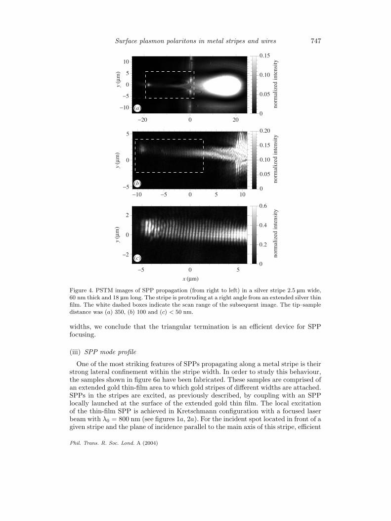
As discussed, the straight termination of the silver stripe in figure 4 gives rise toboth SPP reflection and scattering. We investigate this process with a triangle-shapedstripe termination at the end of a silver stripe 3.5 µm wide and 60 nm thick. ThePSTM image (same illumination parameters as above) is shown in figure 5. Withinthe stripe we observe a lateral intensity distribution which can be readily explainedin terms of SPP reflection at the stripe edges. We also observe an intense brightspot due to forward scattering of the SPP. The intensity distribution of this spot isconfined to an FWHM of 1 µm along the y-direction. As, in the case of a rectangularstripe termination (see figure 4) the scattering spot extends over the whole stripe
Phil. Trans. R. Soc. Lond. A (2004)
Surface plasmon polaritons in metal stripes and wires 747
y(µ
m)
y(µ
m)
10
5
0
−5
−10
5
0
−5
−20 0 20
norm
aliz
ed in
tens
ity
0.15
0.10
0.05
0
0.20
0.15
0.10
0.05
0
norm
aliz
ed in
tens
ity
−10 −5 0 5 10
(a)
(b)
y(µ
m)
2
0
−2
0.6
0.4
0.2
0−5 0 5
x (µm)no
rmal
ized
inte
nsity
(c)
Figure 4. PSTM images of SPP propagation (from right to left) in a silver stripe 2.5 µm wide,60 nm thick and 18 µm long. The stripe is protruding at a right angle from an extended silver thinfilm. The white dashed boxes indicate the scan range of the subsequent image. The tip–sampledistance was (a) 350, (b) 100 and (c) < 50 nm.
widths, we conclude that the triangular termination is an efficient device for SPPfocusing.
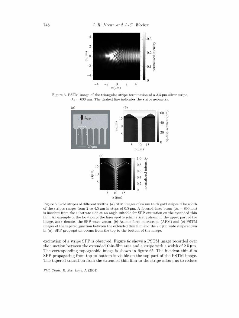
(iii) SPP mode profile
One of the most striking features of SPPs propagating along a metal stripe is theirstrong lateral confinement within the stripe width. In order to study this behaviour,the samples shown in figure 6a have been fabricated. These samples are comprised ofan extended gold thin-film area to which gold stripes of different widths are attached.SPPs in the stripes are excited, as previously described, by coupling with an SPPlocally launched at the surface of the extended gold thin film. The local excitationof the thin-film SPP is achieved in Kretschmann configuration with a focused laserbeam with λ0 = 800 nm (see figures 1a, 2a). For the incident spot located in front of agiven stripe and the plane of incidence parallel to the main axis of this stripe, efficient
Phil. Trans. R. Soc. Lond. A (2004)
748 J. R. Krenn and J.-C. Weeber
y(µ
m)
4
2
0
−2
−4
norm
aliz
ed in
tens
ity
0.3
0.2
0.1
0−4 −2 0 2 4
x (µm)
Figure 5. PSTM image of the triangular stripe termination of a 3.5 µm silver stripe,λ0 = 633 nm. The dashed line indicates the stripe geometry.
kSPP
20µmx (µm)
y(µ
m)
15
10
5
15
10
5
y(µ
m)
5 10 15
5 10 15x (µm)
60
40
20
0 tip d
ispl
acem
ent (
nm)
norm
aliz
ed in
tens
ity1.0
0.8
0.6
0.4
0.2
0
(a) (b)
(c)
Figure 6. Gold stripes of different widths. (a) SEM images of 55 nm thick gold stripes. The widthof the stripes ranges from 2 to 4.5 µm in steps of 0.5 µm. A focused laser beam (λ0 = 800 nm)is incident from the substrate side at an angle suitable for SPP excitation on the extended thinfilm. An example of the location of the laser spot is schematically shown in the upper part of theimage, kSPP denotes the SPP wave vector. (b) Atomic force microscope (AFM) and (c) PSTMimages of the tapered junction between the extended thin film and the 2.5 µm wide stripe shownin (a). SPP propagation occurs from the top to the bottom of the image.
excitation of a stripe SPP is observed. Figure 6c shows a PSTM image recorded overthe junction between the extended thin-film area and a stripe with a width of 2.5 µm.The corresponding topographic image is shown in figure 6b. The incident thin-filmSPP propagating from top to bottom is visible on the top part of the PSTM image.The tapered transition from the extended thin film to the stripe allows us to reduce
Phil. Trans. R. Soc. Lond. A (2004)

Surface plasmon polaritons in metal stripes and wires 749
w = 2500 nmp = 480 nm
w = 1500 nmp = 530 nm
w = 3500 nmp = 580 nm
observation plane
z
xy
w
norm
aliz
ed i
nten
sity
norm
aliz
ed i
nten
sity
norm
aliz
ed i
nten
sity
0 5 10 15
0 5 10 150 5 10 15
0.4
0.2
0
0.8
0.6
0.4
0.2
0
0.4
0.3
0.2
0.1
0
x (µm)
x (µm)x (µm)
Figure 7. Cross-cuts of the near-field intensity distributions recorded at a constant height overthree of the stripes (widths 3.5, 2.5 and 4.5 µm) shown in figure 6. The dashed lines are topo-graphic profiles indicating the stripes’ widths and allowing the estimation of the lateral confine-ment of the optical profiles. The values of p give the period of the oscillations observed in theoptical profiles.
the scattering of the incident SPP at the thin-film edges and to improve the SPPexcitation efficiency on the stripe. The strong lateral confinement of the stripe SPPis unambiguously demonstrated in figure 6c by comparing the geometrical width ofthe stripe, as measured in the topographic image (figure 6b), with the width of thenear-field intensity distribution recorded over the stripe. We note that the length ofthe stripe considered in this case is 50 µm, while an 18 µm long stripe was used inthe experiment shown in figure 4. Thus, because the amplitude of the incident stripeSPP is small when back-reflected at the stripe termination, no significant standing-wave pattern is visible on the PSTM image. Thanks to the very weak contrast of theinterference fringes, one can see in figure 6c that the optical response of the stripeexhibits a longitudinal structure parallel to the stripe axis.
In order to study the dependence of this SPP modal structure as a function ofstripe width, a PSTM image of each stripe shown in figure 6a has been recorded. Aselection of transverse cross-cuts (along the x-axis) of these near-field optical imagesare displayed in figure 7. The topographic stripe profiles (dashed lines in figure 7)superimposed on these cross-cuts allow us to observe the strong lateral confinementof the optical response of each stripe (except for the stripe with w = 1.5 µm). Figure 7shows that the near-field intensity distribution of the SPP mode propagating on the
Phil. Trans. R. Soc. Lond. A (2004)
750 J. R. Krenn and J.-C. Weeber
||k(b)
(c)(d)
y (µ
m)
x (µm) x (µm)
y (µ
m)
10 5 0
−5 −10
5
0
−5
−10−20 0 20 −10 −5 0 5
0.4 0.3 0.2 0.1 0
0.6
0.4
0.2
0
norm
aliz
ed in
tens
ity
norm
aliz
ed in
tens
ity
(a)
20µm10µm
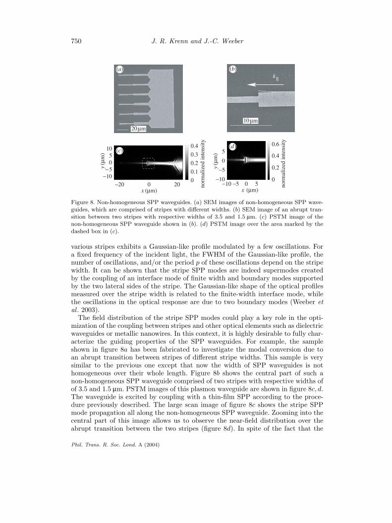
Figure 8. Non-homogeneous SPP waveguides. (a) SEM images of non-homogeneous SPP wave-guides, which are comprised of stripes with different widths. (b) SEM image of an abrupt tran-sition between two stripes with respective widths of 3.5 and 1.5 µm. (c) PSTM image of thenon-homogeneous SPP waveguide shown in (b). (d) PSTM image over the area marked by thedashed box in (c).
various stripes exhibits a Gaussian-like profile modulated by a few oscillations. Fora fixed frequency of the incident light, the FWHM of the Gaussian-like profile, thenumber of oscillations, and/or the period p of these oscillations depend on the stripewidth. It can be shown that the stripe SPP modes are indeed supermodes createdby the coupling of an interface mode of finite width and boundary modes supportedby the two lateral sides of the stripe. The Gaussian-like shape of the optical profilesmeasured over the stripe width is related to the finite-width interface mode, whilethe oscillations in the optical response are due to two boundary modes (Weeber etal . 2003).
The field distribution of the stripe SPP modes could play a key role in the opti-mization of the coupling between stripes and other optical elements such as dielectricwaveguides or metallic nanowires. In this context, it is highly desirable to fully char-acterize the guiding properties of the SPP waveguides. For example, the sampleshown in figure 8a has been fabricated to investigate the modal conversion due toan abrupt transition between stripes of different stripe widths. This sample is verysimilar to the previous one except that now the width of SPP waveguides is nothomogeneous over their whole length. Figure 8b shows the central part of such anon-homogeneous SPP waveguide comprised of two stripes with respective widths ofof 3.5 and 1.5 µm. PSTM images of this plasmon waveguide are shown in figure 8c, d.The waveguide is excited by coupling with a thin-film SPP according to the proce-dure previously described. The large scan image of figure 8c shows the stripe SPPmode propagation all along the non-homogeneous SPP waveguide. Zooming into thecentral part of this image allows us to observe the near-field distribution over theabrupt transition between the two stripes (figure 8d). In spite of the fact that the
Phil. Trans. R. Soc. Lond. A (2004)
Surface plasmon polaritons in metal stripes and wires 751
10µm
y
x
(a) (b) (c)
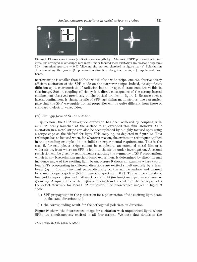
Figure 9. Fluorescence images (excitation wavelength λ0 = 514 nm) of SPP propagation in fourcross-like arranged silver stripes (see inset) under focused local excitation (microscope objective50×, numerical aperture = 0.7) following the method sketched in figure 1c. (a) Polarizationdirection along the y-axis; (b) polarization direction along the x-axis; (c) unpolarized laserbeam.
narrow stripe is smaller than half the width of the wide stripe, one can observe a veryefficient excitation of the SPP mode on the narrower stripe. Indeed, no significantdiffusion spot, characteristic of radiation losses, or spatial transients are visible inthis image. Such a coupling efficiency is a direct consequence of the strong lateralconfinement observed previously on the optical profiles in figure 7. Because such alateral confinement is characteristic of SPP-sustaining metal stripes, one can antici-pate that the SPP waveguide optical properties can be quite different from those ofstandard dielectric waveguides.
(iv) Strongly focused SPP excitation
Up to now, the SPP waveguide excitation has been achieved by coupling withan SPP locally launched at the surface of an extended thin film. However, SPPexcitation in a metal stripe can also be accomplished by a highly focused spot usinga stripe edge as the ‘defect’ for light–SPP coupling, as depicted in figure 1c. Thistechnique has to be used when, for whatever reason, the excitation techniques appliedin the preceding examples do not fulfil the experimental requirements. This is thecase if, for example, a stripe cannot be coupled to an extended metal film or awider stripe, from where an SPP is fed into the stripe under investigation. A secondrestriction can be given by requirements regarding the symmetry of SPP propagation,which in any Kretschmann method-based experiment is determined by direction andincidence angle of the exciting light beam. Figure 9 shows an example where two orfour SPPs propagating in different directions are excited simultaneously by a laserbeam (λ0 = 514 nm) incident perpendicularly on the sample surface and focusedby a microscope objective (50×, numerical aperture = 0.7). The sample consists offour gold stripes (3 µm wide, 70 nm thick and 14 µm long) arranged in a cross-likegeometry. A square hole with 1.5 µm side length in the centre of the cross providesthe defect structure for local SPP excitation. The fluorescence images in figure 9show
(i) SPP propagation in the y-direction for a polarization of the exciting light beamin the same direction; and
(ii) the corresponding result for the orthogonal polarization direction.
Figure 9c shows the fluorescence image for excitation with unpolarized light, whereSPPs are simultaneously excited in all four stripes. We note that details in the
Phil. Trans. R. Soc. Lond. A (2004)
752 J. R. Krenn and J.-C. Weeber
2µm
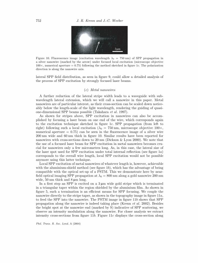
Figure 10. Fluorescence image (excitation wavelength λ0 = 750 nm) of SPP propagation ina silver nanowire (marked by the arrow) under focused local excitation (microscope objective100×, numerical aperture = 0.75) following the method sketched in figure 1c. The polarizationdirection is along the nanowire axis.
lateral SPP field distribution, as seen in figure 9, could allow a detailed analysis ofthe process of SPP excitation by strongly focused laser beams.
(c) Metal nanowires
A further reduction of the lateral stripe width leads to a waveguide with sub-wavelength lateral extension, which we will call a nanowire in this paper. Metalnanowires are of particular interest, as their cross-section can be scaled down notice-ably below the length-scale of the light wavelength, rendering the guiding of quasi-one-dimensional SPP beams possible (Takahara et al . 1997).
As shown for stripes above, SPP excitation in nanowires can also be accom-plished by focusing a laser beam on one end of the wire, which corresponds againto the excitation technique sketched in figure 1c. SPP propagation (from left toright) following such a local excitation (λ0 = 750 nm, microscope objective 100×,numerical aperture = 0.75) can be seen in the fluorescence image of a silver wire200 nm wide and 60 nm thick in figure 10. Similar results have been reported fornanowires with cross-sections down to 20 nm (Dickson & Lyon 2000). We note thatthe use of a focused laser beam for SPP excitation in metal nanowires becomes cru-cial for nanowires only a few micrometres long. As, in this case, the lateral size ofthe laser spot used for SPP excitation under total internal reflection (see figure 1a)corresponds to the overall wire length, local SPP excitation would not be possibleanymore using this latter technique.
Local SPP excitation of metal nanowires of whatever length is, however, achievablewith the aluminium-shield method (see figure 1b), which has the advantage of beingcompatible with the optical set-up of a PSTM. This we demonstrate here by near-field optical imaging SPP propagation at λ0 = 800 nm along a gold nanowire 200 nmwide, 50 nm thick and 8 µm long.
In a first step an SPP is excited on a 3 µm wide gold stripe which is terminatedin a triangular taper within the region shielded by the aluminium film. As shown infigure 5, such a termination is an efficient means for SPP focusing. We couple thenanowire directly to the stripe taper, as shown in the topography image in figure 11a,to feed the SPP into the nanowire. The PSTM image in figure 11b shows that SPPpropagation along the nanowire is indeed taking place (Krenn et al . 2002). Besidesthe bright spot at the nanowire end (marked by S) indicative of SPP scattering, weobserve an intensity modulation along the nanowire. For closer analysis we extractintensity cross-sections from figure 11b. Figure 11c displays the cross-section along
Phil. Trans. R. Soc. Lond. A (2004)

Surface plasmon polaritons in metal stripes and wires 753
S
1
2
nanowire length (µm)0
1
2
3
4
5
inte
nsity
(ar
b. u
nits
)
0
2
4
6
distance (µm)
inte
nsity
(ar
b. u
nits
)
heig
ht (
nm)
1
2
2 µm
(a)
(b)
(c)
(d)
1.5
1.0
0.5
0 1 2 3 4 5 6 7
1 2 3 4 5 6 7 8 9
0.5 1.0 1.5 2.0
50
40
30
20
10
00
Figure 11. SPP propagation in a silver nanowire. (a) Topography; (b) simultaneously acquiredPSTM image. S marks SPP scattering at the nanowire termination. (c) Cross-cut (solid line)along the nanowire as indicated by the horizontal arrows and the number 1 in (b). The dashedline is an exponential fit yielding LSPP = 2.5 µm. The inset shows a corresponding cross-cut(solid line) from a nanowire with a length of 20 µm but otherwise identical geometry to thenanowire shown in (a). Again, we find LSPP = 2.5 µm by an exponential fit (dashed line).(d) Solid line, cross-cut as indicated by the vertical arrows and the number 2 in (b); dottedline, topography profile of the nanowire taken from an SEM image (not shown), combined withheight information from (a).
the nanowire as marked by the arrows and the number 1 in figure 11b. Apart fromsome distortion along the first micrometre along the nanowire due to the presenceof the taper, we find an overall decrease in SPP intensity with distance (solid line),which can be fitted as an exponential intensity decay with a corresponding LSPP valueof 2.5 µm (dashed line). Furthermore, the intensity along the nanowire is found to bemodulated with a periodicity of half the SPP wavelength, as calculated for a gold–airinterface (Raether 1988). As in the case of the silver stripe in figure 4 this modulationthus corresponds to interference between the SPP propagating along the nanowirefrom left to right and a counterpropagating SPP due to reflection at the nanowiretermination. This interpretation is further supported by the SPP intensity profilealong a gold nanowire identical to that shown in figure 11a except for a length of20 µm. As shown in the inset of figure 11c, LSPP is again found to be 2.5 µm but inthis case no interference pattern is observed. This finding is readily explained by thelength of the nanowire leading to an SPP intensity at the nanowire termination thathas already strongly decayed so that practically no SPP reflection occurs. Our resultsdemonstrate that the wavelength of the SPP mode we observe on the nanowire equalsthe wavelength of SPP modes on micrometre-wide stripes.
Phil. Trans. R. Soc. Lond. A (2004)
754 J. R. Krenn and J.-C. Weeber
An intensity cross-cut in the direction perpendicular to the wire axis is shown infigure 11d. Apart from a central peak we observe a rather broad and shallow intensityprofile, which we found to depend on the geometry of the taper-coupling stripe andnanowire (other taper geometries not shown here). We therefore assign this signal toSPP scattering at the taper edges and concentrate on the sharp central peak, whichhas an FWHM of only 115 nm, corresponding to ≈ λ0/7. The intensity drops sharplynear the nanowire edges so that cross-talk between closely packed nanowires can beexpected to be accordingly low (Krenn et al . 2002). This result clearly demonstratesthe nanoscale waveguiding properties of gold nanowires.
4. Summary and outlook
The precise control of metal stripe and wire geometries by lithographic means allowsthe realization of efficient SPP waveguides. The lithographic process together withvarious schemes for local light–SPP coupling and SPP field imaging constitutes apowerful toolbox to investigate these waveguides. We have shown that properlydesigned stripes and wires can be used to propagate, couple and focus SPPs. Thedirect observation of the SPP mode structure opens the way to an improved under-standing of SPP propagation in confined geometries. Although the SPP propagationdistances have been found to be restricted to distances of the order of 10 µm, applica-tions for SPP waveguides in highly miniaturized and integrated optical and electro-optical devices can be envisaged. Indeed, the observed strong spatial confinement ofSPP modes to metal stripes and wires allows in principle unprecedented integrationdensities. As SPPs are surface waves the fabrication of such devices could rely onthe quasi-2D fabrication techniques that are well established within the electronicsindustry.The authors thank F. R. Aussenegg, A. Dereux, H. Ditlbacher, N. Felidj, A. Hohenau, B. Lam-precht, A. Leitner, M. Salerno and G. Schider, who have contributed to the results describedin this review. The Austrian Ministry of Technology and the Austrian Science Foundation areacknowledged for financial support.
References
Barnes, W. L., Preist, T. W., Kitson, S. C. & Sambles, J. R. 1996 Physical origin of photonicenergy gaps in the propagation of surface plasmons on gratings. Phys. Rev. B54, 6227–6244.
Berini, P. 1999 Plasmon–polariton modes guided by a metal film of finite width. Opt. Lett. 24,1011–1013.
Bouhelier, A., Huser, T., Tamaru, H., Guntherodt, H. J., Pohl, D. W., Baida, F. I. & Van Labeke,D. 2001 Plasmon optics of structured silver films. Phys. Rev. B63, 155 404.
Bozhevolnyi, S. I. & Coello, V. 1998 Elastic scattering of surface plasmon polaritons: modellingand experiment. Phys. Rev. B58, 10 899–10 910.
Bozhevolnyi, S. I. & Pudonin, F. A. 1997 Two-dimensional micro-optics of surface plasmons.Phys. Rev. Lett. 78, 2823–2826.
Bozhevolnyi, S. I., Erland, J. E., Leosson, K., Skovgaard, P. M. W. & Hvam, J. M. 2001 Wave-guiding in surface plasmon polariton band-gap structures. Phys. Rev. Lett. 86, 3008–3011.
Courjon, D., Sarayedine, K. & Spajer, M. 1989 Scanning tunneling optical microscopy. Opt.Commun. 71, 23–28.
Dawson, P., de Fornel, F. & Goudonnet, J. P. 1994 Imaging of surface plasmon propagationand edge interaction using a photon scanning tunneling microscope. Phys. Rev. Lett. 72,2927–2930.
Phil. Trans. R. Soc. Lond. A (2004)
Surface plasmon polaritons in metal stripes and wires 755
Dereux, A., Girard, C. & Weeber, J. C. 2000 Theoretical principles of near-field optical micro-scopies and spectroscopies. J. Chem. Phys. 112, 7775–7789.
Dickson, R. M. & Lyon, L. A. 2000 Unidirectional plasmon propagation in metallic nanowires.J. Phys. Chem. B104, 6095–6098.
Ditlbacher, H., Krenn, J. R., Felidj, N., Lamprecht, B., Schider, G., Salerno, M., Leitner, A. &Aussenegg, F. R. 2002a Fluorescence imaging of surface plasmon fields. Appl. Phys. Lett. 80,404–406.
Ditlbacher, H., Krenn, J. R., Schider, G., Leitner, A. & Aussenegg, F. R. 2002b Two-dimensionaloptics with surface plasmon polaritons. Appl. Phys. Lett. 81, 1762–1764.
Ebbesen, T. W., Lezec, H. J., Ghaemi, H. F., Thio, T. & Wolff, P. A. 1998 Extraordinary opticaltransmission through sub-wavelength hole arrays. Nature 391, 667–669.
Krenn, J. R., Wolf, R., Leitner, A. & Aussenegg, F. R. 1997 Near-field optical imaging thesurface plasmon fields around lithographically designed nanostructures. Opt. Commun. 137,46–50.
Krenn, J. R. (and 10 others) 1999 Squeezing the optical near-field zone by plasmon coupling ofmetallic nanoparticles. Phys. Rev. Lett. 82, 2590–2593.
Krenn, J. R., Lamprecht, B., Ditlbacher, H., Schider, G., Salerno, M., Leitner, A. & Aussenegg,F. R. 2002 Non-diffraction limited light transport by gold nanowires. Europhys. Lett. 60,663–669.
Lamprecht, B., Krenn, J. R., Schider, G., Ditlbacher, H., Salerno, M., Felidj, N., Leitner, A.,Aussenegg, F. R. & Weeber, J. C. 2001 Surface plasmon propagation in microscale metalstripes. Appl. Phys. Lett. 79, 51–53.
McCord, M. A. & Rooks, M. J. 1997 Handbook of microlithography, micromachining and micro-fabrication (ed P. Rai-Choudhury), vol. 1, ch. 2, pp. 139–249. Bellingham, WA: SPIE andThe Institution of Electrical Engineers.
Maier, S. A., Kik, P. G., Atwater, H. A., Meltzer, S., Harel, E., Koel, B. E. & Requicha, A. A. G.2003 Local detection of electromagnetic energy transport below the diffraction limit in metalnanoparticle plasmon waveguides. Nature Mater. 2, 229–232.
Pincemin, F. & Greffet, J. J. 1996 Propagation and localization of a surface plasmon polaritonon a finite grating. J. Opt. Soc. Am. B13, 1499–1509.
Pincemin, F., Maradudin, A. A., Boardman, A. D. & Greffet, J. J. 1994 Scattering of a surfaceplasmon polariton by a surface defect. Phys. Rev. B50, 15 261–15 275.
Quidant, R., Weeber, J. C., Dereux, A., Peyrade, D., Colas des Francs, G., Girard, C. & Chen, Y.2001 Addressing and imaging high optical index dielectric ridges in the optical near field. Phys.Rev. E64, 066607.
Quidant, R., Weeber, J. C., Dereux, A., Peyrade, Chen, Y. & Girard, C. 2002 Near-field observa-tion of evanescent light wave coupling in sub-wavelength optical waveguides. Europhys. Lett.57, 191–197.
Raether, H. 1988 Surface plasmons. Springer.Reddick, R. C., Warmack, R. J. & Ferrell, T. L. 1989 New form of scanning optical microscopy.
Phys. Rev. B39, 767–770.Sanchez-Gil, J. A. 1996 Coupling, resonance transmission and tunneling of surface-plasmon
polaritons through metallic gratings of finite length. Phys. Rev. B53, 10 317–10 327.Sanchez-Gil, J. A. 1998 Surface defect scattering of surface plasmon polaritons: mirrors and
light emitters. Appl. Phys. Lett. 73, 3509–3511.Schroter, U. & Heitmann, D. 1998 Surface-plasmon-enhanced transmission through metallic
gratings. Phys. Rev. B58, 15 419–15 421.Smolyaninov, I. I., Mazzoni, D. L. & Davis, C. C. 1996 Imaging of surface plasmon scattering
by lithographically created individual surface defects. Phys. Rev. Lett. 77, 3877–3880.Smolyaninov, I. I., Mazzoni, D. L., Mait, J. & Davis, C. C. 1997 Experimental study of surface-
plasmon scattering by individual surface defects. Phys. Rev. B56, 1601–1611.
Phil. Trans. R. Soc. Lond. A (2004)

756 J. R. Krenn and J.-C. Weeber
Takahara, J., Yamagishi, S., Taki, H., Morimoto, A. & Kobayashi, T. 1997 Guiding of a one-dimensional optical beam with nanometer diameter. Opt. Lett. 22, 475–477.
Weeber, J. C., Bourillot, E., Dereux, A., Goudonnet, J. P., Chen, Y. & Girard, C. 1996 Obser-vation of light confinement effects with a near-field optical microscope. Phys. Rev. Lett. 77,5332–5335.
Weeber, J. C., Lacroute, Y. & Dereux, A. 2003 Optical near-field distributions of surface plasmonwaveguide modes. Phys. Rev. B68, 115401.
Weeber, J. C., Krenn, J. R., Dereux, A., Lamprecht, B., Lacroute, Y. & Goudonnet, J. P. 2001Near-field observation of surface plasmon polariton propagation on thin metal stripes. Phys.Rev. B64, 045411.
Phil. Trans. R. Soc. Lond. A (2004)