Embed Size (px)
Citation preview

Terahertz Science and Technology, ISSN 1941-7411 Vol.6, No.2, June 2013
147
Invited Paper
THz and microwave surface plasmon polaritons on ultrathin corrugated metallic strips
Tie Jun Cui * and Xiaopeng Shen State Key Laboratory of Millimetre Waves, School of Information Science and Engineering, Southeast University,
Nanjing 210096, China * Email: [email protected]
(Received May 2, 2013)
Abstract: In the terahertz and microwave frequencies, natural surface plasmon polaritons (SPPs) do not exist, but can be supported by plasmonic metamaterials, which are usually periodic structures decorated on metallic surfaces. In this review paper, we introduce a kind of planar or flexible plasmonic metamaterial on thin metal films with nearly zero thickness. From theoretical simulations and experiments, we demonstrate that spoof SPPs can propagate along an ultrathin corrugated metallic strip and be highly sustained along two orthogonal directions of the strip in the terahertz and microwave regions with excellent performance, such as broadband, good modal shape, long propagation distance, and low bending loss. We also show that such ultrathin corrugated metallic strip can be printed on flexible dielectric film to support conformal surface plasmons (CSPs) on arbitrary surfaces. The ability to bend spoof SPPs freely makes the ultrathin plasmonic metamaterial more practical to produce plasmonic devices. We have designed and simulated broadband planar and flexible SPP waveguide, 90o bend, beam splitter, and ring resonator in the terahertz frequency, which exhibit excellent performance. Experiments in the microwave frequency validate the feasibility of the ultrathin plasmonic metamaterial.
Keywords: Terahertz metamaterials, Surface plasmon polaritons, Conformal surface plasmons, Plasmonic devices
doi: 10.11906/TST.147-164.2013.06.09
1. Introduction
Natural surface plasmon polaritons (SPPs) occur at the optical frequencies (visible or ultraviolet), which have attracted great attentions and have been intensively investigated due to their specific features and huge application potentials [1-8]. SPPs are highly localized surface waves propagating in a direction parallel to the interface of air and metal [9], which behaves like plasma with a negative permittivity below the plasma frequency in the optical range. The highly-localized feature of SPPs makes it possible to overcome diffraction limit and realize miniaturized photonic components and integrated circuits, which have found wide applications in nano-photonics and optoelectronics [10-14]. However, in the terahertz and microwave frequency bands, the natural SPPs do not exist since the metal does not have a negative permittivity while

Terahertz Science and Technology, ISSN 1941-7411 Vol.6, No.2, June 2013
148
behaves like a perfect electric conductor (PEC) [9]. On PEC surfaces, it has been shown that Sommerfeld or Zenneck surface waves appear, which have weak confinement on the surfaces and short propagating distance [15-17]. To realize the spoof SPPs or designer SPPs at the terahertz and microwave frequencies, plasmonic metamaterials have been proposed, which are usually generated by decorating periodic arrays of subwavelength grooves, holes, or blocks on metal surfaces [18-24]. Nevertheless, the currently existing plasmonic metamaterials have the following disadvantages. First, they are non-planar structures with vertical dimensions above or below the metal surfaces, yielding the inconvenience for fabrications and integration. Second, they cannot control the bending of surface waves freely. Hence the existing plasmonic metamaterials are difficult to realize plasmonic devices and circuits. In fact, the natural SPPs can neither be controlled to propagate along an arbitrarily- designed path freely on metal surfaces in the optical frequency.
Among the spoof SPP structures in the microwave and terahertz frequencies, the one-dimensional periodic array of grooves (infinitely long) on the metal surface [18] much attraction to propagate SPP waves. However, the infinite thickness along the groove direction makes it impossible to be used in practice. In order to produce compact SPP waveguides and components, the thickness has then been shrunk to subwavelength scales [25-29]. It has been shown that the three-dimensional SPP waveguide with subwavelength thickness can support very good SPP waves, from which a series of terahertz SPP devices have been proposed with experiment verification in the microwave frequencies, such as the bidirectional and multi-directional terahertz SPP splitters [25-27] with rectangular grooves, a broadband terahertz slow-wave system, and bidirectional terahertz SPP splitter with highly transverse confinement and bending SPP splitter [28, 29].
Although the three-dimensional SPP waveguide and components with subwavelength thickness make a big step towards applications, they are still inconvenient to be integrated. To reach this purpose, the thickness has been further shrunk to nearly zero [30, 31]. In this paper, we will review the recent work on the ultrathin spoof SPP waveguides and components designed for the microwave and terahertz frequencies. In details, we will introduce a kind of planar or flexible plasmonic metamaterials on thin metal films with nearly zero thickness. We will demonstrate that spoof SPPs can propagate along an ultrathin corrugated metallic strip with high localization and excellent performance. We will also show that such ultrathin corrugated metallic strip can be printed on flexible dielectric film to support conformal surface plasmons (CSPs) on arbitrarily-shaped surfaces. As examples, we have designed and simulated broadband planar and flexible SPP waveguide, 90o bend, beam splitter, and ring resonator in the terahertz frequency, and verified them by experiments in the microwave frequencies.

Terahertz Science and Technology, ISSN 1941-7411 Vol.6, No.2, June 2013
149
2. Planar SPP waveguides and components
The proposed plasmonic metamaterial is a free-standing structure [30], as shown in the inset of Fig.1. A periodic array of edge grooves with depth d, width a, lattice constant p, and height h is corrugated on a perfectly conducting metal plate with thickness t. We employ the full-wave finite-element method to numerically calculate the dispersion curves of the TM-polarized waves propagating in the x direction along the corrugated metal plate. Fig. 1 illustrates the dispersion relations for the fundamental mode, which associates the frequency with the axial propagation constant kin the x axis. The mode properties of spoof SPPs can be controlled by the geometrical parameters of groove. Here we choose p=50 mm , a=20 mm , d=40 mm , h=50 mm , and six values of thickness t (infinite, 1000, 100, 10, 1, and 0.01 mm ), respectively, to make spoof SPPs propagate in the terahertz frequency. The black curve is the light line, and the blue curve shows the theoretical dispersion of infinite thickness [18]. As illustrated by the f-k relations in Fig. 1, the dispersion curves significantly deviate from the light line, indicating that the periodic structured metal plate is capable of confining EM waves on the surface. The waves are loosely bound for small k, but become more tightly bound as kis becomes larger.
Fig. 1 Dispersion relations of the spoof SPPs in plasmonic metamaterials with different thicknesses [30]. The black line indicates the light line, the blue line shows the theoretical dispersion with infinite thickness in the y direction, and other lines are for five values of thickness: t=1000, 100, 10, 1 and 0.01 mm .The inset displays the corrugated metal plate with p = h = 50 mm , d = 40 mm , and a = 20 mm .
As the thickness t decreases, the dispersion curve makes further deviation from the light line and the cutoff frequency becomes lower, implying stronger confinement of surface waves on thinner corrugated metal plate, as shown in Fig. 1, which has inverse tendency to the dispersion relation with varying lateral widths of Domino plasmons standing on a metal ground [24]. It is

Terahertz Science and Technology, ISSN 1941-7411 Vol.6, No.2, June 2013
150
very interesting and important that the dispersion curve keeps unchanged as the thickness is below 1 mm , suggesting that the plasmonic modes should be insensitive to the variation of thickness and can be highly confined on a thin metal film with nearly zero thickness. In this paper, we emphasize our study on the structured thin metal film with nearly zero thickness (t= 0.01 mm ), which is termed as the planar plasmonic metamaterial to manipulate the propagation of SPPs and integrate plasmonic components in the subwavelength scale on a plane. The planar plasmonic metamaterial has a better ability to confine the SPP modes than the 3D structures with large thickness. From Fig. 1, its propagation constant is bigger than the wave vector in vacuum in the frequency ranging from 0.7 THz to 1.2 THz, implying strong confinement of SPPs. As the frequency increases above 1.3 THz, the SPP modes are strongly localized on the surface and cannot propagate.
The confinement and propagation characteristics of spoof SPPs on the planar plasmonic metamaterial have been verified by full-wave simulations in the terahertz regime. Fig. 2a illustrates the spatial variation of electric field (Ez) on an x-y plane, which is 2 mm above the metal film, along an 8000 mm -long planar plasmonic metamaterial waveguide at 1.0 THz, showing excellent SPP propagation. The detailed SPP modes (on y-z plane) located at x=500 mm and 7500 mm are demonstrated in Figs. 2b and 2c, in which the left and right panels represent the Ey and Ez components, respectively. Figs. 2d and 2e display the field distributions of SPP modes along two orthogonal cuts (dashed lines in Figs. 2b and 2c). From these figures, we observe the following unique features of planar plasmonic metamaterial: 1) Along the propagating (x) direction, SPPs propagate nearly losslessly and their modal shapes are almost unchanged after travelling a long distance; 2) Along the vertical (z) direction, SPPs are highly confined with exponential decays of e-|z|/13 on both sides of film; 3) Along the transverse (y) direction, the field values keep constantly large in the vicinity of film edges (50 mm <y<53.5 mm or -3.5 mm <y<0, see Fig. 2d) and decay exponentially beyond the vicinity with e(y+3.5)/13.12 (y<3.5 mm ) and e-(y-53.5)/14 (y>53.5 mm ). Such features indicate that the planar plasmonic metamaterial can efficiently sustain broadband terahertz waves in two orthogonal directions with exponential decays at subwavelength scale (about 1/15 wavelength) and guide the waves to propagate without loss. On one hand, the highly orthogonal confinement of SPPs makes the planar plasmonic metamaterial feasible to bend EM waves freely, and hence control EM waves in a plane. On the other hand, the constantly high field value in the vicinity of film edge provides possibility to couple EM waves between different planar plasmonic metamaterials. The other simulation results from 0.7 THz to 1.1 THz are demonstrated in Fig. 3 showing the wideband property of the ultrathin SPP structure.
The scale invariance of classical electromagnetism indicates that the dispersion relations of the planar plasmonic metamaterial can be scaled down to the microwave frequency. Scaled up by 100 times of the proposed structure, it performs excellent SPP propagation characteristics in the

Terahertz Science and Technology, ISSN 1941-7411 Vol.6, No.2, June 2013
151
frequency ranging from 7 GHz to 11 GHz. Using the printed circuit board (PCB) technology, a 200 mm long, 5 mm wide, and 0.018 mm thick corrugated copper strip is etched on a 0.1 mm-thick substrate with dielectric constant 2.65 and loss tangent 0.001 (Fig. 2f). Two monopoles are used as the source and detector, respectively. The detector is fixed at 1mm above the sample and moves on the x-y plane to scan the Ez field. The magnitude and phase information of Ez field is recorded by the Agilent N5230C vector network analyzer. The measured electric field at 10 GHz is illustrated in Fig. 2g, which shows that the planar plasmonic metamaterials can efficiently confine the spoof SPPs and maintain a long propagation distance. Similarly, the measurement results from 7 GHz - 11 GHz are presented in Fig. 4 to illustrate the broadband property.
Fig. 2 Numerical simulation (in terahertz) and experiment (in microwave) results of the planar plasmonic waveguide.
(a) The simulated electric field (Ez) of the SPP propagation at 1.0 THz, in which the thickness t = 0.01 mm , and the length of plasmonic waveguide L = 8000 mm . (b-c) The modal distributions of Ey and Ez components on the y-z plane located at x=500 mm and 7500 mm along the plasmonic waveguide. (d-e) The profile distributions of Ey and Ez magnitudes along the white-dot lines marked in b and c, both of which are normalized to the peak value in the cross section. The yellow region in d indicates the width of metal film. (f) Photo of fabricated planar plasmonic waveguide in the microwave frequency, in which the 0.018 mm-thick copper is printed on the 0.15 mm-thick substrate. (g) The measured electric field distribution (Ez) at 10 GHz on the x-y plane, which is 2 mm above the planar metal film.

Terahertz Science and Technology, ISSN 1941-7411 Vol.6, No.2, June 2013
152
Fig. 3 Simulated electric fields (Ez) of the planar plasmonic waveguide in the terahertz frequencies. (a) 0.7 THz; (b) 0.8 THz; (c) 0.9 THz; (d) 1.0 THz; (e) 1.1 THz.
Fig. 4 Measured electric fields (Ez) of the planar plasmonic waveguide in the microwave frequencies. (a) 7 GHz; (b)
8 GHz; (c) 9 GHz; (d) 10 GHz; (e) 11 GHz.
Besides the easy fabrication of planar structures, the powerful ability to bend SPP waves makes the planar plasmonic metamaterial more useful to realize functional plasmonic devices. Based on the proposed planar plasmonic waveguide, we have designed and simulated a 90o SPP bend and a 60o Y-shaped beam splitter in the terahertz regime (see Fig. 5) and implemented experiments in the microwave frequency. As shown in Fig. 5(a), the 90o bend is formed by two

Terahertz Science and Technology, ISSN 1941-7411 Vol.6, No.2, June 2013
153
straight SPP waveguides connected by a curved waveguide along a circular arc of radius 300 mm . The full-wave simulation results of Ez fields from 0.7 THz to 1.1 THz are illustrated in Fig. 6, indicating that the SPP modes experience little loss and the field intensities are nearly unchanged before and after travelling through the circular arc.
Fig. 5 Geometries of the planar plasmonic 90o bend and Y-shaped beam splitter in the terahertz frequency. (a) 90o
bend. (b) Y-shaped beam splitter.
Fig. 6 Simulated electric fields (Ez) of the planar plasmonic 90o bend in the terahertz frequencies. (a) 0.7 THz; (b) 0.8 THz; (c) 0.9 THz; (d) 1.1 THz.
We designed the beam splitter using two symmetrical S-bends, each of which is composed of

Terahertz Science and Technology, ISSN 1941-7411 Vol.6, No.2, June 2013
154
three straight planar plasmonic waveguides with 30o bending angle, as shown in Fig. 5(b). For such a beam splitter, the simulated electric fields Ez in a wide frequency ranging from 0.7 THz to 1.1 THz are demonstrated in Fig. 7, from which we observe that the input power is divided equally into the output arms with almost no loss. From Figs. 6 and 7, we observe that both the 90o bend and Y-shaped splitter have excellent performance over a large frequency range. For validation, the corresponding experiments have been conducted in the microwave frequency. The fabricated samples of the 90o bend and beam splitter are illustrated in Figs. 8(a) and 8(b), respectively. The measured results of the electric fields (Ez) from 7 GHz to 11 GHz are demonstrated in Figs. 9 and 10, which have very good agreements to the simulation results.
Fig. 7 Simulated electric fields (Ez) of the planar plasmonic beam splitter in the terahertz frequencies. (a) 0.7 THz; (b) 0.8 THz; (c) 0.9 THz; (d) 1.1 THz.
Fig. 8 Photos of the fabricated planar plasmonic 90o bend and Y-shaped beam splitter in the microwave frequency. (a) 90o bend. (b) Y-shaped beam splitter.
Using the capability of planar plasmonic metamaterials in freely bending SPP waves and providing efficient coupling, we can design a complicated planar device, the ring resonator, which includes a straight plasmonic waveguide and a ring based on the corrugated metal film, as depicted in Fig. 11(a). The output signals can be modulated by properly choosing the ring’s radius and the coupling efficiency between the plasmonic waveguide and ring. Here, the ring’s

Terahertz Science and Technology, ISSN 1941-7411 Vol.6, No.2, June 2013
155
outside radius is designed as 159.2 mm , which is about half wavelength at the central frequency (1 THz); the gap between the ring and waveguide is optimized as 10 mm to reach the proper coupling strength. In principle, part of the input field is coupled into the ring, and then coupled to the waveguide again after a circulation. The two beams in the right part of waveguide interfere with each other, resulting in the modulation of the output signals.
Fig. 9 Measured electric fields (Ez) of the planar plasmonic 90o bend in the microwave frequencies. (a) 7 GHz; (b) 8 GHz; (c) 9 GHz; (d) 11 GHz.
Fig. 10 Measured electric fields (Ez) of the planar plasmonic beam splitter in the microwave frequencies. (a) 7 GHz; (b) 8 GHz; (c) 9 GHz; (d) 11 GHz.
The phase change around the ring is calculated as 2 ( )2effn Rπφ λ πλ
∆ = , in which λ is the

Terahertz Science and Technology, ISSN 1941-7411 Vol.6, No.2, June 2013
156
wavelength in free space, ( )effn λ is the mode effective index that can be taken from the
dispersion relations in Fig. 1, and R is the ring radius. When 2mφ π∆ = , the interference is constructive, i.e., the ring is at the resonance state and the signal can be transmitted to the output. When (2 1)mφ π∆ = + , the interference is destructive, i.e., the ring resonator works at the closed state, and the signal will be cutoff. In our design, the plasmonic ring resonator is closed at 0.98 THz and active at 1.06 THz. Full-wave simulations of the designed structure clearly demonstrate the two states, as shown in Figs. 12(a) and 12(b). From these figures, we observe that SPP waves travel around the ring smoothly with the fields highly confined although the ring’s radius is only half wavelength.
Fig. 11 A planar plasmonic ring resonator.(a) Geometry in the terahertz frequency. (b) Photo in the microwave frequency.
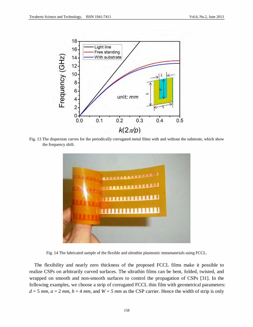
We implement a microwave experiment to test the performance of plasmonic ring resonator. The sample is fabricated in the same PCB substrate as earlier, as shown in Fig. 11(b), in which the straight plasmonic waveguide is 150 mm long, including 20 periods of grooves, the ring’s outer radius is 15.92 mm, and the gap is 1 mm. Figs. 12(c) and 12(d) illustrate the measured electric-field components Ez, which have excellent agreements to the simulation results in physics, showing that the ring resonator switches between active and closed states when tuning the frequency by about 0.7 GHz. We remark that there exist tiny frequency shifts in the microwave experiment due to the use of PCB substrate, in which the plasmonic ring resonator is closed at 9.3 GHz and is active at 10.0 GHz. This can be easily explained by the dispersion relations of planar plasmonic metamaterials with and without substrate, as presented in Fig. 13.

Terahertz Science and Technology, ISSN 1941-7411 Vol.6, No.2, June 2013
157
3. Flexible SPP waveguides and components
Fig. 12 Numerical simulation (in terahertz) and experiment (in microwave) results of the planar ring resonator [30]. (a) The simulated electric field (Ez) at 0.98 THz. (b) The simulated electric field (Ez) at 1.06 THz. (c) The measured electric field (Ez) at 9.3 GHz. (d) The measured electric field (Ez) at 10 GHz.
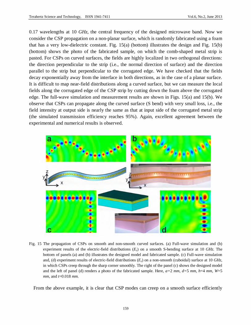
Due to the ultrathin nature of the proposed corrugated metallic strip, we can make flexible SPP waveguides and components [31]. For example, we can manufacture the corresponding plasmonic metamaterials using the standard PCB fabrication process on a three-layered flexible copper clad laminate (FCCL), which consists of a single layer of polyimide and an electrolytic copper clad sheet connected with the epoxy adhesive. The thicknesses of polymide, adhesive and copper foil layers are 12.5, 13, and 18 microns, respectively, and hence the total thickness of the film is 43.5 microns, which is much smaller than the working wavelength in the microwave frequency. As shown in Fig. 14, the fabricated samples are ultrathin and flexible. They can be wrapped around curved surfaces and, therefore, are very well suited for their incorporation into arbitrarily curved surfaces to mould the flow of conformal surface plasmons (CSPs).
Terahertz Science and Technology, ISSN 1941-7411 Vol.6, No.2, June 2013
158
Fig. 13 The dispersion curves for the periodically corrugated metal films with and without the substrate, which show
the frequency shift.
Fig. 14 The fabricated sample of the flexible and ultrathin plasmonic metamaterials using FCCL.
The flexibility and nearly zero thickness of the proposed FCCL films make it possible to realize CSPs on arbitrarily curved surfaces. The ultrathin films can be bent, folded, twisted, and wrapped on smooth and non-smooth surfaces to control the propagation of CSPs [31]. In the following examples, we choose a strip of corrugated FCCL thin film with geometrical parameters: d = 5 mm, a = 2 mm, h = 4 mm, and W = 5 mm as the CSP carrier. Hence the width of strip is only
Terahertz Science and Technology, ISSN 1941-7411 Vol.6, No.2, June 2013
159
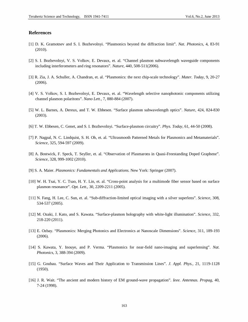
0.17 wavelengths at 10 GHz, the central frequency of the designed microwave band. Now we consider the CSP propagation on a non-planar surface, which is randomly fabricated using a foam that has a very low-dielectric constant. Fig. 15(a) (bottom) illustrates the design and Fig. 15(b) (bottom) shows the photo of the fabricated sample, on which the comb-shaped metal strip is pasted. For CSPs on curved surfaces, the fields are highly localized in two orthogonal directions: the direction perpendicular to the strip (i.e., the normal direction of surface) and the direction parallel to the strip but perpendicular to the corrugated edge. We have checked that the fields decay exponentially away from the interface in both directions, as in the case of a planar surface. It is difficult to map near-field distributions along a curved surface, but we can measure the local fields along the corrugated edge of the CSP strip by cutting down the foam above the corrugated edge. The full-wave simulation and measurement results are shown in Figs. 15(a) and 15(b). We observe that CSPs can propagate along the curved surface (S bend) with very small loss, i.e., the field intensity at output side is nearly the same as that at input side of the corrugated metal strip (the simulated transmission efficiency reaches 95%). Again, excellent agreement between the experimental and numerical results is observed.
Fig. 15 The propagation of CSPs on smooth and non-smooth curved surfaces. (a) Full-wave simulation and (b) experiment results of the electric-field distributions (Ez) on a smooth S-bending surface at 10 GHz. The bottom of panels (a) and (b) illustrates the designed model and fabricated sample. (c) Full-wave simulation and, (d) experiment results of electric-field distributions (Ez) on a non-smooth (cuboidal) surface at 10 GHz, in which CSPs creep through the sharp corner smoothly. The right of the panel (c) shows the designed model and the left of panel (d) renders a photo of the fabricated sample. Here, a=2 mm, d=5 mm, h=4 mm, W=5 mm, and t=0.018 mm.
From the above example, it is clear that CSP modes can creep on a smooth surface efficiently

Terahertz Science and Technology, ISSN 1941-7411 Vol.6, No.2, June 2013
160
with the aid of the flexible FCCL film. Now we want to check the performance of CSPs at sharp edges or corners. Consider a non-smooth cuboidal surface, which contains four sharp edges with 90-degree corners, as illustrated in Fig. 15(c) (right). We have fabricated the cuboidal surface using again the low-dielectric foam, and wrapped the designed FCCL strip around it, as shown in Fig. 15(d) (left). Similar to the previous example, the local fields along the corrugated edge of the comb-shaped strip are mapped, as depicted in Fig. 15(d). The computed E-field map obtained from the full-wave modeling is given in Fig. 15(c). Both simulation and measurement results demonstrate the excellent performance of CSPs when propagating through sharp edges: surface EM waves are creeping through the 90-degree corner smoothly with relatively small bending loss. Such excellent performance does not take place in the standard SPPs, spoof SPPs, and even in the traditional microwave waveguides (bulk and microstrip), in which significant reflections occur at sharp corners.
Due to the flexibility, nearly zero thickness, sub-wavelength width and low-loss propagation, the proposed structures have much more freedom to control the propagation of surface EM waves than previous plasmonic approaches. In the next two examples, we control the CSP waves to propagate around a spiral route and a 3D helix route [31]. The designed model and fabricated sample of the spiral structure is shown in Figs. 16(a) and 16(c), along which the corrugated ultrathin FCCL strip is wrapped. The geometrical parameters are the same as those used in the previous figure. The minimum and maximum radii of the spiral are 20 and 40 mm, respectively. The numerical simulation (Fig. 16(b)) and experiment mapping (Fig. 16(d)) of the local electric fields along the corrugated edge present an excellent agreement, and demonstrate the excellent performance of CSP waves on the very complex spiral surface (the simulated transmission efficiency is as high as 95%) [31]. The comb-shaped metal strip can also be wrapped on a 3D dielectric cylinder to realize helix CSPs, as illustrated in Fig. 17. In this case, the foam cylinder has a radius of 15 mm, and the metallic CSP strip is wrapped spirally around it at a bevel axle of 15 degrees. Fig. 17(a) illustrates the full-wave simulation results of near-filed distributions around the whole helix strip at 11 GHz, showing that CSPs can creep along the helix path with good modal shape and with low attenuation. However, it is difficult to measure the 3D field distributions using the experimental platform. Hence we bury the cylinder wrapped with the helix CSP strip in the foam background, so that the fringe and pillar regions of the strip can be mapped. The near-field distribution at 10 GHz measured on a plane that is placed 1.5 mm above the sample is given in Fig. 17(b). We notice that CSP waves on the output end are nearly the same as those on the input end by passing through the 3D helix path, showing excellent performance.

Terahertz Science and Technology, ISSN 1941-7411 Vol.6, No.2, June 2013
161
Fig. 16 The propagation of spiral CSPs on a spiral surface [31]. (a) The designed model and (c) the actual fabricated sample with a 20-mm curvature radius in the beginning and the maximum curvature radius of 40 mm, in which a=2 mm, d=5 mm, h=4 mm, W=5 mm, and t=0.018 mm. The flexible and ultra-thin comb-shaped metal strip is supported by a foam substrate with nearly unity dielectric constant. (b) Full-wave simulation and, (d) experimental results of near-field distributions (Ez) on the plane which is 1.5 mm above the spiral sample at 11 GHz.
4. Conclusions
From the above simulation and experiment results, it is very important that we only used a strip of planar plasmonic metamaterials, instead of a large area of three-dimensional plasmonic metamaterials, to realize the planar SPP waveguides and plasmonic functional devices, all of which have excellent performance. Hence the proposed planar plasmonic metamaterials can be directly used to design and produce other complicated planar plasmonic components - passive and active, and build up planar plasmonic integrated circuits and systems in the microwave and terahertz frequencies. Using the ultrathin nature, we have also proposed the concept of CSPs and we have presented the design, fabrication, and characterization of these surface EM waves on ultrathin and flexible dielectric films. Thanks to their very-deep subwavelength confinement, CSPs are able to propagate along arbitrarily curved surfaces over long distances with very low absorption and radiation losses. We have experimentally demonstrated that these surface modes

Terahertz Science and Technology, ISSN 1941-7411 Vol.6, No.2, June 2013
162
can be bent, folded, and even twisted to change their polarization state. The flexible, conformal and ultrathin nature of the proposed metamaterial structures make CSPs find very promising applications for novel plasmonic devices, circuits, and systems.
Fig. 17 The propagation of CSPs on a 3D helical-shaped curved surface [31]. The foam cylinder has a radius of 15 mm, and the metallic CSP strip is wrapped spirally around it at a bevel axle of 15 degrees. (a) The designed model (left) and full-wave simulation result (right). (b)The fabricated sample (top) and experimental result (bottom). Both simulation and experimental results are near-field distributions (Ez) on the plane which is 1.5 mm above the cylinder top at 11 GHz. Excellent propagating performance of CSPs along the helical-shaped surface is observed.
The planar and flexible plasmonic metamaterials can be naturally combined to the emerging graphene technology since grapheme is a thin film with nearly zero thickness. Therefore, it is possible to extend the planar and flexible plasmonic metamaterial to the optical frequency using the advanced nano fabrication techniques, to produce the high-performance planar SPP waveguides, plasmonic devices, integrated circuits and systems, finding a new road to applications for graphene.
Acknowledgements
This work was supported in part by the National Science Foundation of China under Grant Nos. 60990320, 60990321, 60990324, 61171024, 61171026, and 61138001, in part by the National High Tech (863) Projects under Grant Nos.2011AA010202 and 2012AA030402, and in part by the 111 Project under the Grant No. 111-2-05.
Terahertz Science and Technology, ISSN 1941-7411 Vol.6, No.2, June 2013
163
References
[1] D. K. Gramotnev and S. I. Bozhevolnyi. “Plasmonics beyond the diffraction limit”. Nat. Photonics, 4, 83-91 (2010).
[2] S. I. Bozhevolnyi, V. S. Volkov, E. Devaux, et. al. “Channel plasmon subwavelength waveguide components including interferometers and ring resonators”. Nature, 440, 508-511(2006).
[3] R. Zia, J. A. Schuller, A. Chandran, et. al. “Plasmonics: the next chip-scale technology”. Mater. Today, 9, 20-27 (2006).
[4] V. S. Volkov, S. I. Bozhevolnyi, E. Devaux, et. al. “Wavelength selective nanophotonic components utilizing channel plasmon polaritons”. Nano Lett., 7, 880-884 (2007).
[5] W. L. Barnes, A. Dereux, and T. W. Ebbesen. “Surface plasmon subwavelength optics”. Nature, 424, 824-830 (2003).
[6] T. W. Ebbesen, C. Genet, and S. I. Bozhevolnyi. “Surface-plasmon circuitry”. Phys. Today, 61, 44-50 (2008).
[7] P. Nagpal, N. C. Lindquist, S. H. Oh, et. al. “Ultrasmooth Patterned Metals for Plasmonics and Metamaterials”. Science, 325, 594-597 (2009).
[8] A. Bostwick, F. Speck, T. Seyller, et. al. “Observation of Plasmarons in Quasi-Freestanding Doped Graphene”. Science, 328, 999-1002 (2010).
[9] S. A. Maier. Plasmonics: Fundamentals and Applications. New York: Springer (2007).
[10] W. H. Tsai, Y. C. Tsao, H. Y. Lin, et. al. “Cross-point analysis for a multimode fiber sensor based on surface plasmon resonance”. Opt. Lett., 30, 2209-2211 (2005).
[11] N. Fang, H. Lee, C. Sun, et. al. “Sub-diffraction-limited optical imaging with a silver superlens”. Science, 308, 534-537 (2005).
[12] M. Ozaki, J. Kato, and S. Kawata. “Surface-plasmon holography with white-light illumination”. Science, 332, 218-220 (2011).
[13] E. Ozbay. “Plasmonics: Merging Photonics and Electronics at Nanoscale Dimensions”. Science, 311, 189-193 (2006).
[14] S. Kawata, Y. Inouye, and P. Verma. “Plasmonics for near-field nano-imaging and superlensing”. Nat. Photonics, 3, 388-394 (2009).
[15] G. Goubau. “Surface Waves and Their Application to Transmission Lines”. J. Appl. Phys., 21, 1119-1128 (1950).
[16] J. R. Wait. “The ancient and modern history of EM ground-wave propagation”. Ieee. Antennas. Propag, 40, 7-24 (1998).

Terahertz Science and Technology, ISSN 1941-7411 Vol.6, No.2, June 2013
164
[17] M. Wachter, M. Nagel, and H. Kurz. “Frequency-dependent characterization of THz Sommerfeld wave propagation on single-wires”. Opt. Express, 13, 10815-10822 (2005).
[18] F. J. Garcia-Vidal, L. Martín-Moreno, and J. B. Pendry. “Surfaces with holes in them: new plasmonic metamaterials”. J. Opt. A-Pure Appl. Op., 7, S97-S101 (2005).
[19] Q. Gan, Y. Gao, K. Wagner, et. al. “Experimental verification of the rainbow trapping effect in adiabatic plasmonic gratings”. Proc. Natl. Acad. Sci., 108, 5169-5173 (2011).
[20] J. B. Pendry, L. Martin-Moreno, and F. J. Garcia-Vidal. “Mimicking surface plasmons with structured surfaces”. Science, 305, 847-848 (2004).
[21] C. R. Williams, S. R. Andrews, S. A. Maier, et. al. “Highly confined guiding of terahertz surface plasmon polaritons on structured metal surfaces”. Nat. Photonics, 2, 175-179 (2008).
[22] A. P. Hibbins, B. R. Evans, and J. R. Sambles. “Experimental verification of designer surface plasmons”. Science, 308, 670-672 (2005).
[23] S. A. Maier, S. R. Andrews, L. Martin-Moreno, et. al. “Terahertz surface plasmon-polariton propagation and focusing on periodically corrugated metal wires”. Phys. Rev. Lett., 97, 176805 (2006).
[24] D. Martin-Cano, M. L. Nesterov, A. I. Fernandez-Dominguez, et. al. “Domino plasmons for subwavelength terahertz circuitry”. Opt. Express, 18, 754-764 (2010).
[25] Y. J. Zhou, Q. Jiang, and T. J. Cui. “Bidirectional surface wave splitters excited by a cylindrical wire”. Opt. Express, 19, 5260-5267 (2011).
[26] Y. J. Zhou and T. J. Cui. “Multidirectional surface-wave splitters”. Appl. Phys. Lett., 98, 221901 (2011).
[27] Y. J. Zhou and T. J. Cui. “Broadband slow-wave systems of subwavelength thickness excited by a metal wire”. Appl. Phys. Lett., 99, 101906 (2011).
[28] Y. J. Zhou, Q. Jiang, and T. J. Cui. “Bidirectional bending splitter of designer surface plasmons”. Appl. Phys. Lett., 99, 111904 (2011).
[29] Y. J. Zhou, Q. Jiang, and T. J. Cui. “Three-dimensional subwavelength components utilizing THz surface plasmons”. Sci. China Inform. Sci., 55, 79-89 (2012).
[30] X. Shen and T. J. Cui. “Planar plasmonic metamaterial on a thin film with nearly zero thickness”. Appl. Phys. Lett., 102, 211909-211904 (2013).
[31] X. P. Shen, T. J. Cui, D. Martin-Cano, et. al. “Conformal surface plasmons propagating on ultrathin and flexible films”. Proc. Natl. Acad. Sci., 110, 40-45 (2013).